EP2133995A1 - Clock data recovery circuit, method and test device utilizing them - Google Patents
Clock data recovery circuit, method and test device utilizing them Download PDFInfo
- Publication number
- EP2133995A1 EP2133995A1 EP08720519A EP08720519A EP2133995A1 EP 2133995 A1 EP2133995 A1 EP 2133995A1 EP 08720519 A EP08720519 A EP 08720519A EP 08720519 A EP08720519 A EP 08720519A EP 2133995 A1 EP2133995 A1 EP 2133995A1
- Authority
- EP
- European Patent Office
- Prior art keywords
- delay
- signal
- phase
- circuit
- data
- Prior art date
- Legal status (The legal status is an assumption and is not a legal conclusion. Google has not performed a legal analysis and makes no representation as to the accuracy of the status listed.)
- Withdrawn
Links
- 238000011084 recovery Methods 0.000 title claims description 51
- 238000012360 testing method Methods 0.000 title claims description 32
- 238000000034 method Methods 0.000 title claims description 16
- 230000010363 phase shift Effects 0.000 claims abstract description 35
- 238000012544 monitoring process Methods 0.000 claims description 7
- 230000001186 cumulative effect Effects 0.000 claims description 5
- 230000003111 delayed effect Effects 0.000 claims description 5
- 238000001914 filtration Methods 0.000 claims description 2
- 238000001514 detection method Methods 0.000 abstract description 10
- 239000000284 extract Substances 0.000 abstract description 4
- 230000005540 biological transmission Effects 0.000 description 9
- 230000001360 synchronised effect Effects 0.000 description 7
- 238000010586 diagram Methods 0.000 description 6
- 230000007274 generation of a signal involved in cell-cell signaling Effects 0.000 description 4
- 238000012986 modification Methods 0.000 description 4
- 230000004048 modification Effects 0.000 description 4
- 239000004065 semiconductor Substances 0.000 description 4
- 238000013459 approach Methods 0.000 description 2
- 230000015572 biosynthetic process Effects 0.000 description 1
- 238000004891 communication Methods 0.000 description 1
- 239000000470 constituent Substances 0.000 description 1
- 230000001934 delay Effects 0.000 description 1
- 230000001419 dependent effect Effects 0.000 description 1
- 238000007689 inspection Methods 0.000 description 1
- 238000003786 synthesis reaction Methods 0.000 description 1
Images


Classifications
-
- H—ELECTRICITY
- H03—ELECTRONIC CIRCUITRY
- H03L—AUTOMATIC CONTROL, STARTING, SYNCHRONISATION OR STABILISATION OF GENERATORS OF ELECTRONIC OSCILLATIONS OR PULSES
- H03L7/00—Automatic control of frequency or phase; Synchronisation
- H03L7/06—Automatic control of frequency or phase; Synchronisation using a reference signal applied to a frequency- or phase-locked loop
- H03L7/08—Details of the phase-locked loop
- H03L7/081—Details of the phase-locked loop provided with an additional controlled phase shifter
-
- H—ELECTRICITY
- H04—ELECTRIC COMMUNICATION TECHNIQUE
- H04L—TRANSMISSION OF DIGITAL INFORMATION, e.g. TELEGRAPHIC COMMUNICATION
- H04L7/00—Arrangements for synchronising receiver with transmitter
- H04L7/02—Speed or phase control by the received code signals, the signals containing no special synchronisation information
- H04L7/033—Speed or phase control by the received code signals, the signals containing no special synchronisation information using the transitions of the received signal to control the phase of the synchronising-signal-generating means, e.g. using a phase-locked loop
-
- G—PHYSICS
- G01—MEASURING; TESTING
- G01R—MEASURING ELECTRIC VARIABLES; MEASURING MAGNETIC VARIABLES
- G01R29/00—Arrangements for measuring or indicating electric quantities not covered by groups G01R19/00 - G01R27/00
- G01R29/02—Measuring characteristics of individual pulses, e.g. deviation from pulse flatness, rise time or duration
-
- G—PHYSICS
- G01—MEASURING; TESTING
- G01R—MEASURING ELECTRIC VARIABLES; MEASURING MAGNETIC VARIABLES
- G01R31/00—Arrangements for testing electric properties; Arrangements for locating electric faults; Arrangements for electrical testing characterised by what is being tested not provided for elsewhere
- G01R31/28—Testing of electronic circuits, e.g. by signal tracer
-
- G—PHYSICS
- G01—MEASURING; TESTING
- G01R—MEASURING ELECTRIC VARIABLES; MEASURING MAGNETIC VARIABLES
- G01R31/00—Arrangements for testing electric properties; Arrangements for locating electric faults; Arrangements for electrical testing characterised by what is being tested not provided for elsewhere
- G01R31/28—Testing of electronic circuits, e.g. by signal tracer
- G01R31/317—Testing of digital circuits
- G01R31/31727—Clock circuits aspects, e.g. test clock circuit details, timing aspects for signal generation, circuits for testing clocks
-
- G—PHYSICS
- G01—MEASURING; TESTING
- G01R—MEASURING ELECTRIC VARIABLES; MEASURING MAGNETIC VARIABLES
- G01R31/00—Arrangements for testing electric properties; Arrangements for locating electric faults; Arrangements for electrical testing characterised by what is being tested not provided for elsewhere
- G01R31/28—Testing of electronic circuits, e.g. by signal tracer
- G01R31/317—Testing of digital circuits
- G01R31/3181—Functional testing
- G01R31/319—Tester hardware, i.e. output processing circuits
- G01R31/3193—Tester hardware, i.e. output processing circuits with comparison between actual response and known fault free response
- G01R31/31937—Timing aspects, e.g. measuring propagation delay
-
- H—ELECTRICITY
- H03—ELECTRONIC CIRCUITRY
- H03L—AUTOMATIC CONTROL, STARTING, SYNCHRONISATION OR STABILISATION OF GENERATORS OF ELECTRONIC OSCILLATIONS OR PULSES
- H03L7/00—Automatic control of frequency or phase; Synchronisation
- H03L7/06—Automatic control of frequency or phase; Synchronisation using a reference signal applied to a frequency- or phase-locked loop
- H03L7/08—Details of the phase-locked loop
- H03L7/081—Details of the phase-locked loop provided with an additional controlled phase shifter
- H03L7/0812—Details of the phase-locked loop provided with an additional controlled phase shifter and where no voltage or current controlled oscillator is used
-
- H—ELECTRICITY
- H04—ELECTRIC COMMUNICATION TECHNIQUE
- H04L—TRANSMISSION OF DIGITAL INFORMATION, e.g. TELEGRAPHIC COMMUNICATION
- H04L25/00—Baseband systems
- H04L25/02—Details ; arrangements for supplying electrical power along data transmission lines
-
- H—ELECTRICITY
- H04—ELECTRIC COMMUNICATION TECHNIQUE
- H04L—TRANSMISSION OF DIGITAL INFORMATION, e.g. TELEGRAPHIC COMMUNICATION
- H04L7/00—Arrangements for synchronising receiver with transmitter
- H04L7/0016—Arrangements for synchronising receiver with transmitter correction of synchronization errors
- H04L7/0033—Correction by delay
- H04L7/0037—Delay of clock signal
Definitions
- the present invention relates to a clock data recovery technique in which bit stream data is regenerated by using a strobe signal.
- serial data transmission In order to transmit/receive data between semiconductor circuits through a small number of data transmission wires, serial data transmission is used.
- a CDR (Clock and Data Recovery) method or a source synchronous method is used.
- serial data is encoded by using the 8B10B encoding or the 4B5B encoding so as not to take the same value continuously over a predetermined period, and a clock signal for synchronization is embedded in the serial data.
- a CDR circuit When a semiconductor circuit outputting serial data is tested as a DUT (Device Under Test), a CDR circuit is provided in the input stage of a semiconductor test apparatus (also simply referred to as a test apparatus).
- the CDR circuit extracts from the serial data a clock signal, which is a reference signal, and generates a strobe signal based on the clock signal to latch each bit data of the serial data.
- the test apparatus determines whether the DUT is good by comparing the regenerated data with an expected value that the data should take.
- Patent Documents 1 and 2 disclose related arts.
- Patent Document 2 discloses the CDR circuit using a PLL (Phase Locked Loop) circuit.
- PLL Phase Locked Loop
- an oscillating frequency of an voltage-controlled oscillator is controlled by feedback such that a phase of the clock signal associated with the serial data and a phase of the strobe signal generated based on the clock signal, are matched with each other.
- the phase of the strobe signal can be adjusted following a jitter of the serial data.
- the present applicant has examined the CDR circuit for the purpose of realizing a function of measuring and tracking a jitter amount of the serial data.
- the applicant has recognized a problem that, if the CDR circuit employing the PLL circuit is used, the frequency of the strobe signal is adjusted, and hence phase information thereof cannot be accurately acquired and the jitter amount that the serial data has cannot be estimated.
- the present invention has been made in view of the foregoing problem, and a purpose of the invention is to provide a clock data recovery technique in which the jitter amount of inputted bit stream data can be measured.
- An embodiment of the present invention relates to a clock data recovery circuit that generates a strobe signal based on a clock signal associated with input data to receive the input data.
- the clock data recovery circuit comprises: a variable delay circuit that provides an initial delay and a shift delay corresponding to a delay control signal, to a reference signal having a predetermined frequency such that a phase of the reference signal is shifted on the basis of the initial delay; a latch circuit that latches each bit data included in the input data by using an output signal of the variable delay circuit as a strobe signal; a phase comparator that matches frequencies of the clock signal and the output signal of the variable delay circuit with each other, and generates phase difference data in accordance with a phase difference between the two signals, the frequencies of which are matched with each other; a loop filter that performs filtering on the phase difference data generated by the phase comparator and outputs the filtered data to the variable delay circuit as the delay control signal; and a phase shift amount acquisition unit that acquires the shift delay provided to the reference signal by the variable
- a phase shift amount from an initial state can be acquired by cumulatively monitoring the delay control signal.
- the shift delay is adjusted by feedback following the input data. Accordingly, according to the embodiment, a jitter amount of the input data (hereinafter, also referred to as a drift amount) can be estimated by acquiring the shift delay.
- the variable delay circuit may reduce an absolute value of the shift delay by an integral multiple of a unit interval of serial data, when the absolute value thereof reaches the integral multiple of the unit interval.
- the phase shift amount provided to the reference signal becomes large accordingly, and hence there could occur a situation in which the phase shift amount may exceed an upper limit of the delay amount that can be added by the variable delay circuit.
- Reduction in the absolute value of the shift delay is equivalent to the fact that the phase shift amount provided to the reference signal is varied so as to approach the initial delay. Therefore, according to the embodiment, the shift delay can follow a large jitter without being limited by the upper limit of the delay amount of the variable delay circuit.
- the delay control signal may take a first state indicating that the phase of the clock signal is advanced or a second state indicating that the phase thereof is delayed.
- the variable delay circuit may reduce the shift delay by a unit period specified by dividing the unit interval by an integer when the delay control signal is in the first state, while may increase the shift delay by the unit period, when the delay control signal is in the second state.
- the phase shift amount acquisition unit may include: an up-down counter that counts up or down in accordance with the state of the delay control signal; and a unit interval shift monitor that detects that a cumulative amount of the shift delay reaches the unit interval by comparing a count value of the up-down counter with a predetermined value.
- the delay control signal may take a third state indicating that there is not any phase difference between the delay control signal and the clock signal. When in the third state, the variable delay circuit may keep a current delay amount.
- the unit interval shift monitor may compare the count value with the predetermined value by monitoring a carry or a borrow in the up-down counter.
- the variable delay circuit may include a buffer chain circuit.
- the delay can be discretely switched by controlling the number of inverters connected together in series.
- the variable delay circuit may include a four-quadrant mixer circuit in which the reference signal and a signal obtained by shifting the phase of the reference signal by 90° are respectively set as an in-phase component (I component) and a quadrature component (Q component), and the delay control signal is subjected to quadrature modulation as a modulation signal.
- the reference signal can be rotated on the IQ plane to provide an optional argument, by varying amplitudes of the I component and Q component in accordance with the delay control signal, allowing the delay to be varied.
- the apparatus comprises any one of the clock data recovery circuits stated above, which is used for receiving the serial data outputted from the DUT. According to the embodiment, the jitter amount of the data outputted from the DUT can be measured.
- the test apparatus may further comprise an expected value generation unit that generates an expected value that output data of the latch circuit in the clock data recovery circuit should take, and a decision unit that compares the expected value with the output data of the latch circuit.
- the expected value generation unit may shift the expected value by one bit in terms of time when detecting that the phase shift amount reaches the unit interval. In this case, even if data to be inputted to the test apparatus is shifted exceeding the unit interval, the decision unit can compare corresponding data items with each other by shifting the expected value in accordance with the data to be inputted.
- Yet another embodiment of the present invention relates to a clock data recovery method in which a strobe signal is generated based on a clock signal associated with input data to receive the input data.
- the method comprises: providing a phase shift to a reference signal having a predetermined frequency by feedback such that the phase thereof is matched with that of the clock signal; latching each bit data included in the input data by using the reference signal provided with the phase shift as a strobe signal; and acquiring cumulatively the phase shift provided to the reference signal.
- a drift amount of the input data can be acquired as a cumulative value of the phase shift.
- the jitter amount of the input data can be measured.
- Fig. 1 is a block diagram illustrating a structure of a test apparatus 100 using a clock data recovery circuit 10 according to an embodiment of the present invention.
- the test apparatus 100 receives serial data S1 outputted from a DUT 110 connected thereto through a transmission path 112, and inspects the DUT 110 by comparing the data S1 with expected value data S13.
- the test apparatus 100 comprises a clock data recovery circuit 10, a comparator 12, an input latch circuit 14, a reference signal generation unit 56, an expected value generation unit 60, a decision unit 62, and an expected value cycle shift unit 64.
- the clock data recovery circuit 10 provided as an input circuit for the test apparatus 100 generates a strobe signal S5 based on serial data S1 inputted to an input terminal 102.
- the reference signal generation unit 56 generates a reference signal S4 that becomes necessary when the clock data recovery circuit 10 generates the strobe signal S5.
- the comparator 12 compares a voltage level of the serial data S1 with a predetermined slice level, and generates data taking a high-level or a low-level (hereinafter, referred to as internal serial data S2).
- the input latch circuit 14 is structured by, for example, a flip-flop and a latch circuit. The input latch circuit 14 latches the internal serial data S2 by using the strobe signal S5 generated by the clock data recovery circuit 10, and synchronizes the data S2 with an internal clock in the test apparatus 100.
- the expected value generation unit 60 generates expected value data S13 that should be taken by output data S12 sequentially outputted from the input latch circuit 14.
- the decision unit 62 compares the data S12 latched by the input latch circuit 14 with the expected value data S13, and measures an error rate, etc., or determines whether the DUT 110 is good.
- the expected value cycle shift unit 64 provided between the expected value generation unit 60 and the expected value cycle shift unit 64 will be described below.
- Fig. 1 illustrates the decision unit 62 as an XOR (eXclusive OR) gate; however, the decision unit 62 can be structured by another circuit element by which bit comparison can be executed.
- the test apparatus 100 is used as follows:
- the DUT 110 is mounted on a socket or the like to be connected to the test apparatus 100.
- a test pattern in a serial form is generated from the DUT 110.
- the test pattern is data to be matched with the expected value data S13.
- the clock data recovery circuit 10 in the test apparatus 100 receives the serial data outputted from the DUT 110 to latch the data by the strobe signal, and determines whether the DUT 110 is good by comparing each bit data with the expected value data.
- the serial data S1 to be inputted to the test apparatus 100 is affected by the inside of the DUT 110 or the transmission path 112, and hence has a jitter.
- the clock data recovery circuit 10 has a function of generating the strobe signal S5 following the jitter of the serial data S1.
- the clock data recovery circuit 10 comprises a change-point detection circuit 16, a phase comparison unit 20, a loop filter 30, a variable delay circuit 40, and a phase shift amount acquisition unit 50.
- the phase comparison unit 20, the loop filter 30 and the variable delay circuit 40 structure a so-called DLL (Delay Locked Loop) circuit.
- the change-point detection circuit 16 extracts a clock signal S3 from the internal serial data S2. For example, when the serial data S1 is encoded in 8B10B format, the change-point detection circuit 16 extracts the clock signal S3 embedded in the serial data S1 based on an edge occurring in the serial data S1.
- the change-point detection circuit 16 is realized by adopting a known technique, and hence detailed descriptions thereof will be omitted.
- the reference signal generation unit 56 generates a reference signal S4 having a predetermined frequency.
- the frequency of the reference signal S4 is set such that the frequency of the strobe signal S5 finally generated by the clock data recovery circuit 10 is matched with the bit rate of the serial data S1.
- the case where the frequency of the reference signal S4 and that of the strobe signal S5 are equal to each other, will be described.
- variable delay circuit 40 To the variable delay circuit 40, are inputted a delay control signal S8a generated by the loop filter 30, which will be described below, and an initial delay set signal S8b for setting an initial delay.
- the variable delay circuit 40 provides a shift delay to the reference signal S4 in accordance with the initial delay and the delay control signal, so that the phase of the reference signal S4 is shifted on the basis of the initial delay. That is, the delay amount provided to the reference signal S4 is defined by synthesis of the initial delay according to the initial delay set signal S8b and the shift delay according to the delay control signal S8a.
- the shift delay according to the delay control signal S8a is negative, it is meant that the phase of the reference signal S4 is more advanced than the initial delay.
- variable delay circuit 40 in Fig. 1 includes a delay control unit 42 and a variable delay element 44.
- the variable delay element 44 receives the reference signal S4, and outputs the signal S4 after providing a delay amount commanded by the delay control unit 42.
- An output of the variable delay element 44 is supplied to the input latch circuit 14 as the strobe signal S5.
- variable delay element 44 may be structured by a buffer chain circuit including a plurality of unit delay elements connected together in cascade, for example, a plurality of inverters, and a switch bypassing each delay element.
- the number of inverters through which the reference signal S4 passes is controlled in accordance with switching on/off of the bypass switch, allowing the delay amount to be adjusted.
- the delay control unit 42 controls the switching on/off in accordance with the delay amount to be provided to the reference signal S4, based on the delay control signal S8a and the initial delay set signal S8b.
- ⁇ t the unit of a delay adjustment with of the variable delay element 44 is denoted by ⁇ t.
- the strobe signal S5 outputted from the variable delay circuit 40 is inputted to the phase comparison unit 20 as well as the input latch circuit 14.
- the phase comparison unit 20 matches the frequency of the clock signal S3 extracted by the change-point detection circuit 16 and that of the strobe signal S5 outputted from the variable delay circuit 40, with each other.
- the phase comparison unit 20 generates phase difference data S9 in accordance with a phase difference between the two signals, the frequencies of which are matched with each other.
- the phase comparison unit 20 includes a phase comparator 22, a first frequency divider 24 and a second frequency divider 26.
- the first frequency divider 24 and the second frequency divider 26 respectively frequency divide the clock signal S3 and the strobe signal S5 at a first and a second frequency dividing ratios, so that a frequency division clock signal S6 and a frequency division strobe signal S5 are generated.
- the phase comparator 22 compares the phases of the frequency division clock signal S6 and the frequency division strobe signal S7, the frequencies of which are equal to each other, and generates the phase difference data S9 in accordance with the phase difference.
- the frequency division ratios of the first frequency divider 24 and the second frequency divider 26 may be set in accordance with a resolution capability for phase comparison by the phase comparator 22, and there are sometimes cases where the first frequency divider 24 or the second frequency divider 26 is not necessary.
- the loop filter 30 is, for example, a low-pass filter, which integrates the phase difference data S9 generated by the phase comparison unit 20 and outputs it to the variable delay circuit 40 as the delay control signal S8a.
- the phase of the strobe signal S5 is adjusted by the DLL circuit so as to follow that of the clock signal S3, allowing each bit of the serial data S1 to be latched.
- the clock data recovery circuit 10 comprises the phase shift amount acquisition unit 50 in addition to the DLL circuit.
- the phase shift amount acquisition unit 50 acquires the delay shift, which is provided to the reference signal S4 by the variable delay circuit 40, by cumulatively monitoring the delay control signal S8a.
- Figs. 2A and 2B are time charts illustrating the serial data S1, the reference signal S4 and the strobe signal S5.
- Fig. 2A illustrates an initial state
- Fig. 2B illustrates a state after a lapse of a certain period from the initial state.
- the vertical axes and the horizontal axes thereof are appropriately enlarged or reduced for better view ability and easy understanding, and therefore illustrated differently from actual scales thereof.
- the reference signal S4 is provided with an initial delay ⁇ 1 by the delay control unit 42. Accordingly, the strobe signal S5 is delayed from the reference signal S4 by the initial delay ⁇ 1.
- the initial delay ⁇ 1 is set in consideration of a set up time and a hold time of the input latch circuit 14.
- Fig. 2B illustrates a state in which the serial data S1 drifts into the direction of being delayed from the initial state by a time ⁇ 2 due to influence of the jitter of the serial data S1. It is noted that the reference signal S4 is not influenced by the jitter of the serial data S1 and any phase shift is not generated, and hence the reference signal S4 is not illustrated in Fig. 2B .
- the clock signal S3 extracted by the change-point detection circuit 16 also drifts by the same time ⁇ 2.
- variable delay circuit 40 provides, to the reference signal S4, a shift delay ⁇ 3 in accordance with the delay control signal S8a, in addition to the initial delay ⁇ 1; and shifts the phase of the reference signal S4 on the basis of the initial delay ⁇ 1.
- the clock data recovery circuit 10 feedback is performed such that a phase difference between the frequency division clock signal S6 and the frequency division strobe signal S7, which respectively correspond to the clock signal S3 and the strobe signal S5, becomes a minimum, causing the shift delay ⁇ 3 to follow the drift time ⁇ 2. That is, even if the serial data S1 has the jitter, the strobe signal S5 following the serial data S1 can be generated, allowing each bit data of the serial data S1 to be latched.
- a first advantage of the clock data recovery circuit 10 in Fig. 1 becomes clear.
- the phase of the clock signal S3 extracted by the change-point detection circuit 16 is varied in accordance with the jitter of the serial data S1.
- the phase of the reference signal S4 is adjusted so as to follow a variation in the phase of the clock signal S3. That is, the shift delay ⁇ 3 provided to the reference signal S4 becomes data indicating the jitter amount (drift time) ⁇ 2 that the serial data S1 has.
- the shift delay ⁇ 3 becomes data in accordance with a cumulative value of the delay control signal S8a, the jitter amount of the serial data S1 can be measured by using the clock data recovery circuit 10 according to the present embodiment.
- the phase shift amount acquisition unit 50 monitors the shift delay ⁇ 3 provided to the reference signal S4 on the basis of the initial delay ⁇ 1.
- the phase shift amount acquisition unit 50 detects that the shift delay ⁇ 3 reaches a value obtained by multiplying a unit interval UI by an integer n, the unit interval UI being defined by a reciprocal of the bit rate of the serial data S1.
- the variable delay circuit 40 varies the phase shift amount provided to the reference signal S4 such that the phase shift amount approaches the initial delay ⁇ 1 by an integral m multiple of the unit interval UI, when an absolute value of the shift delay ⁇ 3 on the basis of the initial delay ⁇ 1, reaches an integral n multiple of the unit interval UI. That is, the absolute value of the shift delay ⁇ 3 is reduced by an integral multiple of the unit interval UI.
- This operation is referred to as a reset operation. It is noted that m may or may not be equal to n.
- the reset operation is executed in which a delay provided to the reference signal S4 becomes the initial delay ⁇ 1, with the shift delay ⁇ 3 being 0.
- Second advantage can be realized by the reset operation.
- a delay amount which can be added to the reference signal S4 is limited in accordance with the number of the inverters to be connected.
- the delay amount that can be added by the variable delay element 44 is ⁇ UI on the basis of the initial delay ⁇ 1
- the jitter amount also referred to as a jitter tolerance
- the serial data S1 which can be followed by the clock data recovery circuit 10
- the clock data recovery circuit 10 When the absolute value of the shift delay ⁇ 3 on the basis of the initial delay ⁇ 1 reaches the unit interval UI, the clock data recovery circuit 10 according to the present embodiment resets the shift delay ⁇ 3 to the initial delay ⁇ 1. Accordingly, the jitter tolerance of the serial data S1 can be a substantially infinite value, without being limited by a range of the delay amount by the variable delay element 44.
- the jitter tolerance required of the test apparatus 100 is specified dependently on a jitter frequency, that is, as the jitter frequency is smaller, the larger jitter tolerance is required. For example, with respect to the jitter frequency of less than or equal to 100 Hz, the jitter tolerance of more than 10 UI is sometimes required. Because the jitter tolerance realized by a clock data recovery circuit using a conventional PLL circuit has at most several UI, the clock data recovery circuit cannot be used in such an application. In contrast, the clock data recovery circuit 10 according to the present embodiment can be preferably used for an application in which the large jitter tolerance is required. Further, when the DUT 110 is a device used for ultra-long distance transmission such as intercontinental communication, the clock data recovery circuit 10 according to the present embodiment can be preferably employed for an application in which the jitter tolerance of tens to hundreds UI is required.
- the delay control signal S8a takes a first state indicating that the phase of the frequency division clock signal S6 is advanced relative to the frequency division strobe signal S7, and a second state indicating that the phase thereof is delayed relative thereto.
- variable delay circuit 40 When the delay control signal S8a is in the first state, the variable delay circuit 40 reduces the delay amount provided to the reference signal S4 by a unit period ⁇ t obtained by dividing the unit interval UI by an integer. The ⁇ t corresponds to a unit adjustment amount of the delay in the variable delay element 44. In contrast, when the delay control signal S8a is in the second state, the variable delay circuit 40 increases the delay provided to the reference signal S4 by the unit period ⁇ t.
- the delay control signal S8a may take a third state indicating that the phases of the frequency division clock signal S6 and the frequency division strobe signal S7 are matched with each other. When the delay control signal S8a takes the third state, the current delay amount is kept without varying the delay provided to the reference signal S4. When the third state is provided for the delay control signal S8a, it can be suppressed that the delay amount fluctuates in a high frequency wave in a state where the phase difference is 0, resulting in an advantage in terms of noise reduction.
- the phase shift amount acquisition unit 50 includes an up-down counter 52 and a UI shift monitor 54.
- Data S10 outputted from the delay control unit 42 indicates a state of the delay control signal S8a.
- the up-down counter 52 counts up or down in accordance with the data S10. That is, a count value of the up-down counter 52 becomes data indicating the shift delay ⁇ 3 relative to the initial delay ⁇ 1.
- the UI shift monitor 54 detects that the shift delay ⁇ 3 reaches the unit interval UI by comparing the count value of the up-down counter 52 with a predetermined value. For example, the UI shift monitor 54 may compare the counter value with the predetermined value by monitoring a carry or a borrow in the up-down counter 52. That is, either one of count-up and count-down occurs more often, the carry or borrow occurs in the up-down counter 52. Accordingly, by appropriately setting the bit value of the counter, it can be detected, as occurrence of the carry or the borrow, that the shift delay ⁇ 3 reaches the unit interval UI.
- the UI shift monitor 54 may be structured by a counter that counts up or down in accordance with the carry or the borrow. In this case, a count value of the UI shift monitor 54 becomes data indicating the jitter corresponding to how many times of the UI has cumulatively occurred since the initial state, allowing the data to be effectively used inside the test apparatus 100. For example, the test apparatus 100 may finish inspection for the DUT 110 based on the data.
- the expected value cycle shift unit 64 is provided between the expected value generation unit 60 and the decision unit 62.
- the expected value cycle shift unit 64 shifts the inputted expected value data S13 by a required number of bits in terms of time.
- the expected value cycle shift unit 64 may be structured by a shift register or a barrel shifter.
- the phase shift amount acquisition unit 50 communicates with the expected value cycle shift unit 64 by control data S15.
- the expected value cycle shift unit 64 shifts the expected value data S13 by one bit in terms of time. With this, an expected value S14 following the jitter of the serial data S1 can be supplied to the decision unit 62.
- the UI shift monitor 54 is structured by a counter, a shift amount of the expected value data S13 provided by the expected value cycle shift unit 64 may be coupled with a count value of the UI shift monitor 54.
- the jitter amount of the serial data S1 can be measured by using the DLL circuit instead of the PLL circuit, and further by providing the phase shift amount acquisition unit 50 that monitors the delay amount.
- the clock data recovery circuit 10 resets the delay amount of the variable delay element 44. With this, limitation of the jitter tolerance by the variable delay element 44 can be eliminated.
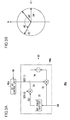
- Figs. 3A and 3B are, respectively, a circuit diagram of a variable delay element 44a in a clock data recovery circuit according to a variation, and an IQ plane diagram illustrating operation thereof.
- the variable delay element 44a is a four-quadrant mixer circuit including a 90° phase shifter 70, a first mixer circuit 72, a second mixer circuit 74, and an adder 76.
- the 90° phase shifter 70 delays the phase of the reference signal S4 by 90°.
- ⁇ 1 in Fig. 3B corresponds to the initial delay ⁇ 1, while ⁇ 3 to the shift delay ⁇ 3 on the basis of the initial delay ⁇ 1.
- a delay control unit 42a outputs cos( ⁇ 1 + ⁇ 3) as I data S22 and sin( ⁇ 1 + ⁇ 3) as Q data S23.
- the first mixer circuit 72 multiplies the I data S22 by the reference signal S4, which is an in-phase signal, while the second mixer circuit 74 multiplies the Q data S23 by a quadrature signal S21.
- the adder 76 adds output signals of the first mixer circuit 72 and the second mixer circuit 74 together.
- variable delay circuit 40a in Fig. 3A when an argument is rotated by 360° in a direction, ⁇ 3 returns to the initial phase ⁇ 1, and hence a substantially infinite jitter tolerance can be realized without performing the aforementioned reset operation. Further, by providing the phase shift amount acquisition unit 50, a drift amount of the serial data S1 can be measured based on the delay control signal S8a.
- the clock data recovery circuit 10 in Fig. 1 or the modified example using the variable delay circuit 40a in Fig. 3A relates to a circuit in which the clock signal S3 embedded in the serial data S1 is extracted to generate the strobe signal S5.
- the present invention can also be applied to a source synchronous method in which the DUT transmits the serial data S1 and the clock signal, synchronized with the serial data S1, at a time.
- the change-point detection circuit 16 is not necessary, and clock signal outputted in synchronized with the serial data S1 from the DUT, may be used as the clock signal S3 for the phase comparison unit 20.
- clock signal S3 for the phase comparison unit 20.
- the source synchronous method if there is not any variation in a relative phase difference between the serial data and the clock signal, there does not occur any transmission error theoretically. In other words, if drift amounts of the serial data and the clock signal are equal to each other, data transmission can be executed even when huge drift occurs. Accordingly, in the case of a test apparatus in which a source synchronous device is used as the DUT, very large jitter tolerance is required.
- the clock data recovery circuit according to the present invention in which there is not any substantial limitation of the jitter tolerance and a jitter amount can be measured, can be preferably applied to the test apparatus 100 for inspecting the source synchronous device.
- the present invention can be applied to tests for semiconductors.
Landscapes
- Engineering & Computer Science (AREA)
- Physics & Mathematics (AREA)
- General Physics & Mathematics (AREA)
- Computer Networks & Wireless Communication (AREA)
- Signal Processing (AREA)
- General Engineering & Computer Science (AREA)
- Power Engineering (AREA)
- Synchronisation In Digital Transmission Systems (AREA)
- Dc Digital Transmission (AREA)
- Stabilization Of Oscillater, Synchronisation, Frequency Synthesizers (AREA)
- Tests Of Electronic Circuits (AREA)
Abstract
A change-point detection circuit 16 extracts a clock signal S3 from serial data S1, input data. A variable delay circuit 40 provides a delay in accordance with a delay control signal S8a to a reference signal S4 having a predetermined frequency, so that the phase of the reference signal S4 is shifted on the basis of an initial delay. An input latch circuit 14 latches internal serial data S2 by using an output signal of the variable delay circuit 40 as a strobe signal S5. A phase comparator 22 matches the frequencies of the clock signal S3 and the strobe signal S5 with each other, and generates phase difference data S9 in accordance with a phase difference between the two signals. A loop filter 30 integrates the phase difference data S9 generated by the phase comparator 22 and outputs it as the delay control signal S8a. The phase shift amount acquisition unit 50 acquires a phase shift amount based on the delay control signal S8a, the phase shift amount being based on the initial delay provided to the reference signal by the variable delay circuit 40.
Description
- The present invention relates to a clock data recovery technique in which bit stream data is regenerated by using a strobe signal.
- In order to transmit/receive data between semiconductor circuits through a small number of data transmission wires, serial data transmission is used. For the serial data transmission, a CDR (Clock and Data Recovery) method or a source synchronous method is used. In the CDR method, serial data is encoded by using the 8B10B encoding or the 4B5B encoding so as not to take the same value continuously over a predetermined period, and a clock signal for synchronization is embedded in the serial data.
- When a semiconductor circuit outputting serial data is tested as a DUT (Device Under Test), a CDR circuit is provided in the input stage of a semiconductor test apparatus (also simply referred to as a test apparatus). The CDR circuit extracts from the serial data a clock signal, which is a reference signal, and generates a strobe signal based on the clock signal to latch each bit data of the serial data. The test apparatus determines whether the DUT is good by comparing the regenerated data with an expected value that the data should take.
Patent Documents - For example,
Patent Document 2 discloses the CDR circuit using a PLL (Phase Locked Loop) circuit. In the circuit, an oscillating frequency of an voltage-controlled oscillator is controlled by feedback such that a phase of the clock signal associated with the serial data and a phase of the strobe signal generated based on the clock signal, are matched with each other. As a result, the phase of the strobe signal can be adjusted following a jitter of the serial data. - [Patent Document 1] Japanese Patent Application Publication No.
Hei 2-62983 - [Patent Document 2] Japanese Patent Application Publication No.
2007-17257 - The present applicant has examined the CDR circuit for the purpose of realizing a function of measuring and tracking a jitter amount of the serial data. However, the applicant has recognized a problem that, if the CDR circuit employing the PLL circuit is used, the frequency of the strobe signal is adjusted, and hence phase information thereof cannot be accurately acquired and the jitter amount that the serial data has cannot be estimated.
- The present invention has been made in view of the foregoing problem, and a purpose of the invention is to provide a clock data recovery technique in which the jitter amount of inputted bit stream data can be measured.
- An embodiment of the present invention relates to a clock data recovery circuit that generates a strobe signal based on a clock signal associated with input data to receive the input data. The clock data recovery circuit comprises: a variable delay circuit that provides an initial delay and a shift delay corresponding to a delay control signal, to a reference signal having a predetermined frequency such that a phase of the reference signal is shifted on the basis of the initial delay; a latch circuit that latches each bit data included in the input data by using an output signal of the variable delay circuit as a strobe signal; a phase comparator that matches frequencies of the clock signal and the output signal of the variable delay circuit with each other, and generates phase difference data in accordance with a phase difference between the two signals, the frequencies of which are matched with each other; a loop filter that performs filtering on the phase difference data generated by the phase comparator and outputs the filtered data to the variable delay circuit as the delay control signal; and a phase shift amount acquisition unit that acquires the shift delay provided to the reference signal by the variable delay circuit, by cumulatively monitoring the delay control signal.
- Because a shift delay amount provided to the reference signal is dependent on the delay control signal, a phase shift amount from an initial state can be acquired by cumulatively monitoring the delay control signal. Herein, the shift delay is adjusted by feedback following the input data. Accordingly, according to the embodiment, a jitter amount of the input data (hereinafter, also referred to as a drift amount) can be estimated by acquiring the shift delay.
- The variable delay circuit may reduce an absolute value of the shift delay by an integral multiple of a unit interval of serial data, when the absolute value thereof reaches the integral multiple of the unit interval.
- As the jitter of the data to be inputted becomes large, the phase shift amount provided to the reference signal becomes large accordingly, and hence there could occur a situation in which the phase shift amount may exceed an upper limit of the delay amount that can be added by the variable delay circuit. Reduction in the absolute value of the shift delay is equivalent to the fact that the phase shift amount provided to the reference signal is varied so as to approach the initial delay. Therefore, according to the embodiment, the shift delay can follow a large jitter without being limited by the upper limit of the delay amount of the variable delay circuit.
- As a result of phase comparison, the delay control signal may take a first state indicating that the phase of the clock signal is advanced or a second state indicating that the phase thereof is delayed. The variable delay circuit may reduce the shift delay by a unit period specified by dividing the unit interval by an integer when the delay control signal is in the first state, while may increase the shift delay by the unit period, when the delay control signal is in the second state. In this case, the phase shift amount acquisition unit may include: an up-down counter that counts up or down in accordance with the state of the delay control signal; and a unit interval shift monitor that detects that a cumulative amount of the shift delay reaches the unit interval by comparing a count value of the up-down counter with a predetermined value. Further, the delay control signal may take a third state indicating that there is not any phase difference between the delay control signal and the clock signal. When in the third state, the variable delay circuit may keep a current delay amount.
- The unit interval shift monitor may compare the count value with the predetermined value by monitoring a carry or a borrow in the up-down counter.
- The variable delay circuit may include a buffer chain circuit. In this case, the delay can be discretely switched by controlling the number of inverters connected together in series.
- The variable delay circuit may include a four-quadrant mixer circuit in which the reference signal and a signal obtained by shifting the phase of the reference signal by 90° are respectively set as an in-phase component (I component) and a quadrature component (Q component), and the delay control signal is subjected to quadrature modulation as a modulation signal. In this case, the reference signal can be rotated on the IQ plane to provide an optional argument, by varying amplitudes of the I component and Q component in accordance with the delay control signal, allowing the delay to be varied.
- Another embodiment of the present invention relates to a test apparatus. The apparatus comprises any one of the clock data recovery circuits stated above, which is used for receiving the serial data outputted from the DUT. According to the embodiment, the jitter amount of the data outputted from the DUT can be measured.
- The test apparatus may further comprise an expected value generation unit that generates an expected value that output data of the latch circuit in the clock data recovery circuit should take, and a decision unit that compares the expected value with the output data of the latch circuit. The expected value generation unit may shift the expected value by one bit in terms of time when detecting that the phase shift amount reaches the unit interval. In this case, even if data to be inputted to the test apparatus is shifted exceeding the unit interval, the decision unit can compare corresponding data items with each other by shifting the expected value in accordance with the data to be inputted.
- Yet another embodiment of the present invention relates to a clock data recovery method in which a strobe signal is generated based on a clock signal associated with input data to receive the input data. The method comprises: providing a phase shift to a reference signal having a predetermined frequency by feedback such that the phase thereof is matched with that of the clock signal; latching each bit data included in the input data by using the reference signal provided with the phase shift as a strobe signal; and acquiring cumulatively the phase shift provided to the reference signal. According to the embodiment, a drift amount of the input data can be acquired as a cumulative value of the phase shift.
- It is noted that any combination of the aforementioned components or any manifestation of the present invention exchanged between methods, devices and so forth, is effective as an embodiment of the present invention.
- According to the present invention, the jitter amount of the input data can be measured.
-
-
Fig. 1 is a block diagram illustrating a structure of a test apparatus using a clock data recovery circuit according to an embodiment of the present invention; -
Figs. 2A and 2B are time charts illustrating serial data, a reference signal and a strobe signal; and -
Figs. 3A and 3B are, respectively, a circuit diagram of a variable delay element in a clock data recovery circuit according to a variation, and an IQ plane diagram illustrating operation thereof. -
- 10
- CLOCK DATA RECOVERY CIRCUIT
- 12
- COMPARATOR
- 14
- INPUT LATCH CIRCUIT
- 16
- CHANGE-POINT DETECTION CIRCUIT
- 20
- PHASE COMPARISON UNIT
- 22
- PHASE COMPARATOR
- 24
- FIRST FREQUENCY DIVIDER
- 26
- SECOND FREQUENCY DIVIDER
- 30
- LOOP FILTER
- 40
- VARIABLE DELAY CIRCUIT
- 42
- DELAY CONTROL UNIT
- 44
- VARIABLE DELAY ELEMENT
- 50
- PHASE SHIFT AMOUNT ACQUISITION UNIT
- 52
- UP-DOWN COUNTER
- 54
- UI SHIFT MONITOR
- 56
- REFERENCE SIGNAL GENERATION UNIT
- 60
- EXPECTED VALUE GENERATION UNIT
- 62
- DECISION UNIT
- 64
- EXPECTED VALUE CYCLE SHIFT UNIT
- 100
- TEST APPARATUS
- 102
- INPUT TERMINAL
- 110
- DUT
- 112
- TRANSMISSION PATH
- S1
- SERIAL DATA
- S2
- INTERNAL SERIAL DATA
- S3
- CLOCK SIGNAL
- S4
- REFERENCE SIGNAL
- S5
- STROBE SIGNAL
- S6
- FREQUENCY DIVISION CLOCK SIGNAL
- S7
- FREQUENCY DIVISION STROBE SIGNAL
- S8A
- DELAY CONTROL SIGNAL
- S8B
- INITIAL DELAY SET SIGNAL
- S9
- PHASE DIFFERENCE DATA
- The present invention will now be described based on preferred embodiments with reference to the accompanying drawings. The same or equivalent constituents, member, or processes illustrated in each drawing will be denoted with the same reference numerals, and the duplicative descriptions thereof are appropriately omitted. The preferred embodiments do not intend to limit the scope of the invention but exemplify the invention. All of the features and the combinations thereof described in the embodiments are not necessarily essential to the invention.
-
Fig. 1 is a block diagram illustrating a structure of atest apparatus 100 using a clockdata recovery circuit 10 according to an embodiment of the present invention. Thetest apparatus 100 receives serial data S1 outputted from aDUT 110 connected thereto through atransmission path 112, and inspects theDUT 110 by comparing the data S1 with expected value data S13. - Outline of the whole structure of the
test apparatus 100 will be described at first. Thetest apparatus 100 comprises a clockdata recovery circuit 10, acomparator 12, aninput latch circuit 14, a reference signal generation unit 56, an expectedvalue generation unit 60, adecision unit 62, and an expected valuecycle shift unit 64. The clockdata recovery circuit 10 provided as an input circuit for thetest apparatus 100 generates a strobe signal S5 based on serial data S1 inputted to aninput terminal 102. The reference signal generation unit 56 generates a reference signal S4 that becomes necessary when the clockdata recovery circuit 10 generates the strobe signal S5. - The
comparator 12 compares a voltage level of the serial data S1 with a predetermined slice level, and generates data taking a high-level or a low-level (hereinafter, referred to as internal serial data S2). Theinput latch circuit 14 is structured by, for example, a flip-flop and a latch circuit. Theinput latch circuit 14 latches the internal serial data S2 by using the strobe signal S5 generated by the clockdata recovery circuit 10, and synchronizes the data S2 with an internal clock in thetest apparatus 100. - The expected
value generation unit 60 generates expected value data S13 that should be taken by output data S12 sequentially outputted from theinput latch circuit 14. Thedecision unit 62 compares the data S12 latched by theinput latch circuit 14 with the expected value data S13, and measures an error rate, etc., or determines whether theDUT 110 is good. The expected valuecycle shift unit 64 provided between the expectedvalue generation unit 60 and the expected valuecycle shift unit 64 will be described below.Fig. 1 illustrates thedecision unit 62 as an XOR (eXclusive OR) gate; however, thedecision unit 62 can be structured by another circuit element by which bit comparison can be executed. - Outline of the whole structure of the
test apparatus 100 has been described above. Thetest apparatus 100 is used as follows: TheDUT 110 is mounted on a socket or the like to be connected to thetest apparatus 100. A test pattern in a serial form is generated from theDUT 110. The test pattern is data to be matched with the expected value data S13. The clockdata recovery circuit 10 in thetest apparatus 100 receives the serial data outputted from theDUT 110 to latch the data by the strobe signal, and determines whether theDUT 110 is good by comparing each bit data with the expected value data. - Hereinafter, the structure of the clock
data recovery circuit 10 provided as an input circuit will be described in detail. The serial data S1 to be inputted to thetest apparatus 100 is affected by the inside of theDUT 110 or thetransmission path 112, and hence has a jitter. The clockdata recovery circuit 10 has a function of generating the strobe signal S5 following the jitter of the serial data S1. - The clock
data recovery circuit 10 comprises a change-point detection circuit 16, aphase comparison unit 20, aloop filter 30, avariable delay circuit 40, and a phase shiftamount acquisition unit 50. Thephase comparison unit 20, theloop filter 30 and thevariable delay circuit 40 structure a so-called DLL (Delay Locked Loop) circuit. - The change-
point detection circuit 16 extracts a clock signal S3 from the internal serial data S2. For example, when the serial data S1 is encoded in 8B10B format, the change-point detection circuit 16 extracts the clock signal S3 embedded in the serial data S1 based on an edge occurring in the serial data S1. The change-point detection circuit 16 is realized by adopting a known technique, and hence detailed descriptions thereof will be omitted. - The reference signal generation unit 56 generates a reference signal S4 having a predetermined frequency. The frequency of the reference signal S4 is set such that the frequency of the strobe signal S5 finally generated by the clock
data recovery circuit 10 is matched with the bit rate of the serial data S1. In the present embodiment, the case where the frequency of the reference signal S4 and that of the strobe signal S5 are equal to each other, will be described. - To the
variable delay circuit 40, are inputted a delay control signal S8a generated by theloop filter 30, which will be described below, and an initial delay set signal S8b for setting an initial delay. Thevariable delay circuit 40 provides a shift delay to the reference signal S4 in accordance with the initial delay and the delay control signal, so that the phase of the reference signal S4 is shifted on the basis of the initial delay. That is, the delay amount provided to the reference signal S4 is defined by synthesis of the initial delay according to the initial delay set signal S8b and the shift delay according to the delay control signal S8a. When the shift delay according to the delay control signal S8a is negative, it is meant that the phase of the reference signal S4 is more advanced than the initial delay. - To realize the function, the
variable delay circuit 40 inFig. 1 includes adelay control unit 42 and avariable delay element 44. Thevariable delay element 44 receives the reference signal S4, and outputs the signal S4 after providing a delay amount commanded by thedelay control unit 42. An output of thevariable delay element 44 is supplied to theinput latch circuit 14 as the strobe signal S5. - For example, the
variable delay element 44 may be structured by a buffer chain circuit including a plurality of unit delay elements connected together in cascade, for example, a plurality of inverters, and a switch bypassing each delay element. In this case, the number of inverters through which the reference signal S4 passes is controlled in accordance with switching on/off of the bypass switch, allowing the delay amount to be adjusted. Thedelay control unit 42 controls the switching on/off in accordance with the delay amount to be provided to the reference signal S4, based on the delay control signal S8a and the initial delay set signal S8b. Hereinafter, the unit of a delay adjustment with of thevariable delay element 44 is denoted by Δt. - The strobe signal S5 outputted from the
variable delay circuit 40 is inputted to thephase comparison unit 20 as well as theinput latch circuit 14. Thephase comparison unit 20 matches the frequency of the clock signal S3 extracted by the change-point detection circuit 16 and that of the strobe signal S5 outputted from thevariable delay circuit 40, with each other. Thephase comparison unit 20 generates phase difference data S9 in accordance with a phase difference between the two signals, the frequencies of which are matched with each other. - To realize this function, the
phase comparison unit 20 includes aphase comparator 22, afirst frequency divider 24 and asecond frequency divider 26. Thefirst frequency divider 24 and thesecond frequency divider 26 respectively frequency divide the clock signal S3 and the strobe signal S5 at a first and a second frequency dividing ratios, so that a frequency division clock signal S6 and a frequency division strobe signal S5 are generated. Thephase comparator 22 compares the phases of the frequency division clock signal S6 and the frequency division strobe signal S7, the frequencies of which are equal to each other, and generates the phase difference data S9 in accordance with the phase difference. - The frequency division ratios of the
first frequency divider 24 and thesecond frequency divider 26 may be set in accordance with a resolution capability for phase comparison by thephase comparator 22, and there are sometimes cases where thefirst frequency divider 24 or thesecond frequency divider 26 is not necessary. - The
loop filter 30 is, for example, a low-pass filter, which integrates the phase difference data S9 generated by thephase comparison unit 20 and outputs it to thevariable delay circuit 40 as the delay control signal S8a. - The phase of the strobe signal S5 is adjusted by the DLL circuit so as to follow that of the clock signal S3, allowing each bit of the serial data S1 to be latched. The clock
data recovery circuit 10 according to the present embodiment comprises the phase shiftamount acquisition unit 50 in addition to the DLL circuit. The phase shiftamount acquisition unit 50 acquires the delay shift, which is provided to the reference signal S4 by thevariable delay circuit 40, by cumulatively monitoring the delay control signal S8a. - Operation of the clock
data recovery circuit 10 structured as stated above will be described.Figs. 2A and 2B are time charts illustrating the serial data S1, the reference signal S4 and the strobe signal S5.Fig. 2A illustrates an initial state, whileFig. 2B illustrates a state after a lapse of a certain period from the initial state. In the following drawings, the vertical axes and the horizontal axes thereof are appropriately enlarged or reduced for better view ability and easy understanding, and therefore illustrated differently from actual scales thereof. - In the initial state, the reference signal S4 is provided with an initial delay τ1 by the
delay control unit 42. Accordingly, the strobe signal S5 is delayed from the reference signal S4 by the initial delay τ1. The initial delay τ1 is set in consideration of a set up time and a hold time of theinput latch circuit 14. -
Fig. 2B illustrates a state in which the serial data S1 drifts into the direction of being delayed from the initial state by a time τ2 due to influence of the jitter of the serial data S1. It is noted that the reference signal S4 is not influenced by the jitter of the serial data S1 and any phase shift is not generated, and hence the reference signal S4 is not illustrated inFig. 2B . When the serial data S1 drifts, the clock signal S3 extracted by the change-point detection circuit 16 also drifts by the same time τ2. As stated above, thevariable delay circuit 40 provides, to the reference signal S4, a shift delay τ3 in accordance with the delay control signal S8a, in addition to the initial delay τ1; and shifts the phase of the reference signal S4 on the basis of the initial delay τ1. - In the clock
data recovery circuit 10, feedback is performed such that a phase difference between the frequency division clock signal S6 and the frequency division strobe signal S7, which respectively correspond to the clock signal S3 and the strobe signal S5, becomes a minimum, causing the shift delay τ3 to follow the drift time τ2. That is, even if the serial data S1 has the jitter, the strobe signal S5 following the serial data S1 can be generated, allowing each bit data of the serial data S1 to be latched. - From the aforementioned descriptions, a first advantage of the clock
data recovery circuit 10 inFig. 1 becomes clear. The phase of the clock signal S3 extracted by the change-point detection circuit 16 is varied in accordance with the jitter of the serial data S1. Also, the phase of the reference signal S4 is adjusted so as to follow a variation in the phase of the clock signal S3. That is, the shift delay τ3 provided to the reference signal S4 becomes data indicating the jitter amount (drift time) τ2 that the serial data S1 has. Herein, because the shift delay τ3 becomes data in accordance with a cumulative value of the delay control signal S8a, the jitter amount of the serial data S1 can be measured by using the clockdata recovery circuit 10 according to the present embodiment. - Subsequently, a reset operation executed by the phase shift
amount acquisition unit 50 and thevariable delay circuit 40 will be described. - As stated above, the phase shift
amount acquisition unit 50 monitors the shift delay τ3 provided to the reference signal S4 on the basis of the initial delay τ1. The phase shiftamount acquisition unit 50 detects that the shift delay τ3 reaches a value obtained by multiplying a unit interval UI by an integer n, the unit interval UI being defined by a reciprocal of the bit rate of the serial data S1. - The
variable delay circuit 40 varies the phase shift amount provided to the reference signal S4 such that the phase shift amount approaches the initial delay τ1 by an integral m multiple of the unit interval UI, when an absolute value of the shift delay τ3 on the basis of the initial delay τ1, reaches an integral n multiple of the unit interval UI. That is, the absolute value of the shift delay τ3 is reduced by an integral multiple of the unit interval UI. This operation is referred to as a reset operation. It is noted that m may or may not be equal to n. - For example, when n=m=1 and when the shift delay τ3 becomes the unit interval UI, the reset operation is executed in which a delay provided to the reference signal S4 becomes the initial delay τ1, with the shift delay τ3 being 0. When m=2, n=1 and when the shift delay τ3 becomes -2 x UI, the shift delay τ3 is set to -UI through the reset operation. The case where m=n holds means that the shift delay τ3 becomes 0 through the reset operation, and hence the phase after the reset operation is set to the initial delay τ1.
- Second advantage can be realized by the reset operation. For example, when the
variable delay element 44 is structured by the buffer chain circuit, a delay amount, which can be added to the reference signal S4, is limited in accordance with the number of the inverters to be connected. For example, when the delay amount that can be added by thevariable delay element 44 is ±UI on the basis of the initial delay τ1, the jitter amount (also referred to as a jitter tolerance) of the serial data S1, which can be followed by the clockdata recovery circuit 10, becomes ±UI. - When the absolute value of the shift delay τ3 on the basis of the initial delay τ1 reaches the unit interval UI, the clock
data recovery circuit 10 according to the present embodiment resets the shift delay τ3 to the initial delay τ1. Accordingly, the jitter tolerance of the serial data S1 can be a substantially infinite value, without being limited by a range of the delay amount by thevariable delay element 44. - The jitter tolerance required of the
test apparatus 100 is specified dependently on a jitter frequency, that is, as the jitter frequency is smaller, the larger jitter tolerance is required. For example, with respect to the jitter frequency of less than or equal to 100 Hz, the jitter tolerance of more than 10 UI is sometimes required. Because the jitter tolerance realized by a clock data recovery circuit using a conventional PLL circuit has at most several UI, the clock data recovery circuit cannot be used in such an application. In contrast, the clockdata recovery circuit 10 according to the present embodiment can be preferably used for an application in which the large jitter tolerance is required. Further, when theDUT 110 is a device used for ultra-long distance transmission such as intercontinental communication, the clockdata recovery circuit 10 according to the present embodiment can be preferably employed for an application in which the jitter tolerance of tens to hundreds UI is required. - Subsequently, an structural example and operation of the phase shift
amount acquisition unit 50 will be described below. In the present embodiment, the delay control signal S8a takes a first state indicating that the phase of the frequency division clock signal S6 is advanced relative to the frequency division strobe signal S7, and a second state indicating that the phase thereof is delayed relative thereto. - When the delay control signal S8a is in the first state, the
variable delay circuit 40 reduces the delay amount provided to the reference signal S4 by a unit period Δt obtained by dividing the unit interval UI by an integer. The Δt corresponds to a unit adjustment amount of the delay in thevariable delay element 44. In contrast, when the delay control signal S8a is in the second state, thevariable delay circuit 40 increases the delay provided to the reference signal S4 by the unit period Δt. The delay control signal S8a may take a third state indicating that the phases of the frequency division clock signal S6 and the frequency division strobe signal S7 are matched with each other. When the delay control signal S8a takes the third state, the current delay amount is kept without varying the delay provided to the reference signal S4. When the third state is provided for the delay control signal S8a, it can be suppressed that the delay amount fluctuates in a high frequency wave in a state where the phase difference is 0, resulting in an advantage in terms of noise reduction. - The phase shift
amount acquisition unit 50 includes an up-down counter 52 and a UI shift monitor 54. Data S10 outputted from thedelay control unit 42 indicates a state of the delay control signal S8a. The up-down counter 52 counts up or down in accordance with the data S10. That is, a count value of the up-down counter 52 becomes data indicating the shift delay τ3 relative to the initial delay τ1. - The UI shift monitor 54 detects that the shift delay τ3 reaches the unit interval UI by comparing the count value of the up-
down counter 52 with a predetermined value. For example, the UI shift monitor 54 may compare the counter value with the predetermined value by monitoring a carry or a borrow in the up-down counter 52. That is, either one of count-up and count-down occurs more often, the carry or borrow occurs in the up-down counter 52. Accordingly, by appropriately setting the bit value of the counter, it can be detected, as occurrence of the carry or the borrow, that the shift delay τ3 reaches the unit interval UI. - The UI shift monitor 54 may be structured by a counter that counts up or down in accordance with the carry or the borrow. In this case, a count value of the UI shift monitor 54 becomes data indicating the jitter corresponding to how many times of the UI has cumulatively occurred since the initial state, allowing the data to be effectively used inside the
test apparatus 100. For example, thetest apparatus 100 may finish inspection for theDUT 110 based on the data. - The expected value
cycle shift unit 64 is provided between the expectedvalue generation unit 60 and thedecision unit 62. The expected valuecycle shift unit 64 shifts the inputted expected value data S13 by a required number of bits in terms of time. For example, the expected valuecycle shift unit 64 may be structured by a shift register or a barrel shifter. When the absolute value of the shift delay τ3 reaches the unit interval UI, the phase shiftamount acquisition unit 50 communicates with the expected valuecycle shift unit 64 by control data S15. After receiving the control signal S15, the expected valuecycle shift unit 64 shifts the expected value data S13 by one bit in terms of time. With this, an expected value S14 following the jitter of the serial data S1 can be supplied to thedecision unit 62. If the UI shift monitor 54 is structured by a counter, a shift amount of the expected value data S13 provided by the expected valuecycle shift unit 64 may be coupled with a count value of the UI shift monitor 54. - The structure and operation of the clock
data recovery circuit 10 according to the embodiment have been described above. According to the clockdata recovery circuit 10 inFig. 1 , the jitter amount of the serial data S1 can be measured by using the DLL circuit instead of the PLL circuit, and further by providing the phase shiftamount acquisition unit 50 that monitors the delay amount. - When the jitter amount measured by the phase shift
amount acquisition unit 50, i.e., the shift delay τ3 provided to the reference signal S4, is shifted by a predetermined amount, an integral multiple of the unit interval on the basis of the initial delay τ1, the clockdata recovery circuit 10 resets the delay amount of thevariable delay element 44. With this, limitation of the jitter tolerance by thevariable delay element 44 can be eliminated. - The aforementioned embodiments are intended to be illustrative only. It will be appreciated by those skilled in the art that various modifications to the constituting elements and processes could be developed and that such modifications are within the scope of the present invention. Hereinafter, such modifications will be described.
-
Figs. 3A and 3B are, respectively, a circuit diagram of avariable delay element 44a in a clock data recovery circuit according to a variation, and an IQ plane diagram illustrating operation thereof. Thevariable delay element 44a is a four-quadrant mixer circuit including a 90°phase shifter 70, afirst mixer circuit 72, asecond mixer circuit 74, and anadder 76. - The 90°
phase shifter 70 delays the phase of the reference signal S4 by 90°. ϕ1 inFig. 3B corresponds to the initial delay τ1, while ϕ3 to the shift delay τ3 on the basis of the initial delay τ1. Adelay control unit 42a outputs cos(ϕ1 + ϕ3) as I data S22 and sin(ϕ1 + ϕ3) as Q data S23. Thefirst mixer circuit 72 multiplies the I data S22 by the reference signal S4, which is an in-phase signal, while thesecond mixer circuit 74 multiplies the Q data S23 by a quadrature signal S21. Theadder 76 adds output signals of thefirst mixer circuit 72 and thesecond mixer circuit 74 together. - According to the
variable delay circuit 40a inFig. 3A , when an argument is rotated by 360° in a direction, ϕ3 returns to the initial phase ϕ1, and hence a substantially infinite jitter tolerance can be realized without performing the aforementioned reset operation. Further, by providing the phase shiftamount acquisition unit 50, a drift amount of the serial data S1 can be measured based on the delay control signal S8a. - The clock
data recovery circuit 10 inFig. 1 or the modified example using thevariable delay circuit 40a inFig. 3A relates to a circuit in which the clock signal S3 embedded in the serial data S1 is extracted to generate the strobe signal S5. The present invention can also be applied to a source synchronous method in which the DUT transmits the serial data S1 and the clock signal, synchronized with the serial data S1, at a time. - In this case, the change-
point detection circuit 16 is not necessary, and clock signal outputted in synchronized with the serial data S1 from the DUT, may be used as the clock signal S3 for thephase comparison unit 20. In the case of the source synchronous method, if there is not any variation in a relative phase difference between the serial data and the clock signal, there does not occur any transmission error theoretically. In other words, if drift amounts of the serial data and the clock signal are equal to each other, data transmission can be executed even when huge drift occurs. Accordingly, in the case of a test apparatus in which a source synchronous device is used as the DUT, very large jitter tolerance is required. The clock data recovery circuit according to the present invention, in which there is not any substantial limitation of the jitter tolerance and a jitter amount can be measured, can be preferably applied to thetest apparatus 100 for inspecting the source synchronous device. - In the embodiments, the case where serial data is inputted to the clock
data recovery circuit 10 has been described; however, the present invention is not limited thereto, but can be applied to the cases where various data are inputted as bit streams. - The present invention has been described based on the preferred embodiments; however, it is clear that the embodiments illustrate only the principle and applications of the invention. Accordingly, it is needless to say that various modifications or changes in the arrangement can be made to the embodiments without departing from the spirit of the invention set forth in the appended claims.
- The present invention can be applied to tests for semiconductors.
Claims (9)
- A clock data recovery circuit that generates a strobe signal based on a clock signal associated with input data to receive the input data, the clock data recovery circuit comprising:a variable delay circuit that provides an initial delay and a shift delay corresponding to a delay control signal, to a reference signal having a predetermined frequency such that a phase of the reference signal is shifted on the basis of the initial delay;a latch circuit that latches each bit data included in the input data by using an output signal of the variable delay circuit as a strobe signal;a phase comparator that matches frequencies of the clock signal and the output signal of the variable delay circuit with each other, and generates phase difference data in accordance with a phase difference between the two signals, the frequencies of which are matched with each other;a loop filter that performs filtering on the phase difference data generated by the phase comparator and outputs the filtered data to the variable delay circuit as the delay control signal; anda phase shift amount acquisition unit that acquires the shift delay provided to the reference signal by the variable delay circuit, by cumulatively monitoring the delay control signal.
- The clock data recovery circuit according to claim 1, wherein the variable delay circuit reduces an absolute value of the shift delay by an integral multiple of a unit interval of the input data, when the absolute value of the shift delay reaches the integral multiple of the unit interval.
- The clock data recovery circuit according to claim 2, wherein the delay control signal takes, as a result of phase comparison, a first state indicating that the phase of the clock signal is advanced or a second state indicating that the phase of the clock signal is delayed, and wherein the variable delay circuit reduces the shift delay by a unit period specified by dividing the unit interval by an integer when the delay control signal is in the first state, while increasing the shift delay by the unit period when the delay control signal is in the second state, and wherein the phase shift amount acquisition unit includes an up-down counter that counts up or down in accordance with the state of the delay control signal, and a unit interval shift monitor that detects that a cumulative amount of the shift delay reaches the unit interval by comparing a count value of the up-down counter with a predetermined value.
- The clock data recovery circuit according to claim 3, wherein the unit interval shift monitor compares the count value with the predetermined value by monitoring a carry or a borrow in the up-down counter.
- The clock data recovery circuit according to any one of claims 1 to 4, wherein the variable delay circuit includes a buffer chain circuit.
- The clock data recovery circuit according to any one of claims 1 to 4, wherein the variable delay circuit includes a four-quadrant mixer circuit in which the reference signal and a signal obtained by shifting the phase of the reference signal by 90° are respectively set as an in-phase component and a quadrature component, and the delay control signal is subjected to quadrature modulation as a modulation signal.
- A test apparatus comprising the clock data recovery circuit according to any one of claims 1 to 6, the clock data recovery circuit being operative to receive serial data outputted from a device under test.
- The test apparatus according to claim 7 further comprising:an expected value generation unit that generates an expected value that output data of the latch circuit in the clock data recovery circuit should take; anda decision unit that compares the expected value with the output data of the latch circuit, wherein the expected value generation unit shifts the expected value by one bit in terms of time when detecting that a cumulative amount of the shift delay reaches the unit interval.
- A clock data recovery method in which a strobe signal is generated based on a clock signal associated with input data to receive the input data, the method comprising:providing a phase shift to a reference signal having a predetermined frequency by feedback such that the phase of the reference signal is matched with that of the clock signal;latching each bit data included in the input data by using the reference signal provided with the phase shift as a strobe signal; andacquiring cumulatively the phase shift provided to the reference signal.
Applications Claiming Priority (2)
| Application Number | Priority Date | Filing Date | Title |
|---|---|---|---|
| JP2007073227 | 2007-03-20 | ||
| PCT/JP2008/000634 WO2008114509A1 (en) | 2007-03-20 | 2008-03-18 | Clock data recovery circuit, method and test device utilizing them |
Publications (1)
| Publication Number | Publication Date |
|---|---|
| EP2133995A1 true EP2133995A1 (en) | 2009-12-16 |
Family
ID=39765627
Family Applications (1)
| Application Number | Title | Priority Date | Filing Date |
|---|---|---|---|
| EP08720519A Withdrawn EP2133995A1 (en) | 2007-03-20 | 2008-03-18 | Clock data recovery circuit, method and test device utilizing them |
Country Status (7)
| Country | Link |
|---|---|
| US (1) | US8537935B2 (en) |
| EP (1) | EP2133995A1 (en) |
| JP (1) | JP5235190B2 (en) |
| KR (1) | KR101120711B1 (en) |
| CN (1) | CN101657966B (en) |
| TW (1) | TWI387768B (en) |
| WO (1) | WO2008114509A1 (en) |
Cited By (1)
| Publication number | Priority date | Publication date | Assignee | Title |
|---|---|---|---|---|
| US8473248B2 (en) | 2009-09-18 | 2013-06-25 | Advantest Corporation | Test apparatus and test method |
Families Citing this family (23)
| Publication number | Priority date | Publication date | Assignee | Title |
|---|---|---|---|---|
| US8156365B2 (en) * | 2008-04-02 | 2012-04-10 | Dongbu Hitek Co., Ltd. | Data reception apparatus |
| KR100928516B1 (en) * | 2008-04-02 | 2009-11-26 | 주식회사 동부하이텍 | display |
| JP2010127692A (en) * | 2008-11-26 | 2010-06-10 | Yokogawa Electric Corp | Timing adjustment device and semiconductor testing apparatus |
| KR20110131765A (en) | 2010-05-31 | 2011-12-07 | 주식회사 하이닉스반도체 | Phase correction circuit and data alignment circuit using the same |
| US8829932B2 (en) * | 2010-07-23 | 2014-09-09 | Fairchild Semiconductor Corporation | No pin test mode |
| JP5952072B2 (en) * | 2012-04-26 | 2016-07-13 | ルネサスエレクトロニクス株式会社 | Encoding device, decoding device, and transmission system |
| KR102006243B1 (en) * | 2012-12-24 | 2019-08-01 | 에스케이하이닉스 주식회사 | Data write circuit of semiconductor apparatus |
| KR20150090486A (en) * | 2014-01-29 | 2015-08-06 | 에스케이하이닉스 주식회사 | Semiconductor test device |
| CN103888132A (en) * | 2014-04-02 | 2014-06-25 | 广东顺德中山大学卡内基梅隆大学国际联合研究院 | Circuit and method for generating two paths of I/Q orthogonal clocks |
| CN107425848B (en) * | 2016-05-23 | 2020-08-11 | 龙芯中科技术有限公司 | Clock data recovery circuit and method |
| JP6906911B2 (en) * | 2016-08-18 | 2021-07-21 | シナプティクス・ジャパン合同会社 | Semiconductor devices, data transmission systems, and operating methods of semiconductor devices |
| CN109891843B (en) * | 2016-09-08 | 2022-03-08 | 美国莱迪思半导体公司 | Computer-implemented method and system for performing the computer-implemented method |
| WO2018137751A1 (en) | 2017-01-24 | 2018-08-02 | Telefonaktiebolaget Lm Ericsson (Publ) | Variable delay circuits |
| KR102502236B1 (en) * | 2017-11-20 | 2023-02-21 | 삼성전자주식회사 | Clock data recovery circuit, apparatus including the same and method for recovery clock and data |
| US10630295B2 (en) * | 2018-04-23 | 2020-04-21 | Synaptics Incorporated | Device and method for detecting signal state transition |
| KR102599059B1 (en) * | 2018-10-11 | 2023-11-08 | 삼성디스플레이 주식회사 | Transition detector and clock data recovery unit including the same |
| KR102674592B1 (en) * | 2020-04-17 | 2024-06-12 | 에스케이하이닉스 주식회사 | System for performing phase matching operation |
| CN115001486A (en) * | 2021-03-01 | 2022-09-02 | 中兴通讯股份有限公司 | Clock data recovery circuit and clock data recovery method |
| US11444746B1 (en) | 2021-06-07 | 2022-09-13 | Analog Devices, Inc. | Phasing detection of asynchronous dividers |
| TWI806539B (en) * | 2022-04-08 | 2023-06-21 | 瑞昱半導體股份有限公司 | Testing system and testing method |
| EP4383573A1 (en) | 2022-12-04 | 2024-06-12 | Lattice Semiconductor Corporation | Clock insertion delay systems and methods |
| JP7811599B2 (en) * | 2024-01-29 | 2026-02-05 | アンリツ株式会社 | Sequence pattern generator and transmission start timing control method therefor |
| JP7737102B1 (en) * | 2025-04-02 | 2025-09-10 | セレブラシステムソリューションズ株式会社 | Data communication circuit |
Family Cites Families (19)
| Publication number | Priority date | Publication date | Assignee | Title |
|---|---|---|---|---|
| JP2688941B2 (en) * | 1988-08-29 | 1997-12-10 | 株式会社アドバンテスト | Phase correction device |
| JPH03289813A (en) * | 1990-04-06 | 1991-12-19 | Nippon Telegr & Teleph Corp <Ntt> | Digital signal delay circuit |
| JPH0854957A (en) * | 1994-08-12 | 1996-02-27 | Hitachi Ltd | Clock distribution system |
| JP3956062B2 (en) * | 1996-07-30 | 2007-08-08 | ソニー株式会社 | Playback apparatus and method |
| JP3718932B2 (en) * | 1996-12-10 | 2005-11-24 | ソニー株式会社 | Intermediate phase clock generation circuit |
| JP2923877B2 (en) * | 1997-01-24 | 1999-07-26 | 日本電気株式会社 | Clock distribution circuit |
| JP3415444B2 (en) * | 1998-06-12 | 2003-06-09 | Necエレクトロニクス株式会社 | Clock control method and circuit |
| JP4259683B2 (en) * | 1998-10-07 | 2009-04-30 | 富士通株式会社 | Phase comparison circuit |
| US6774693B2 (en) * | 2000-01-18 | 2004-08-10 | Pmc-Sierra, Inc. | Digital delay line with synchronous control |
| US6586977B2 (en) | 2000-09-22 | 2003-07-01 | Agere Systems Inc. | Four quadrant analog mixer-based delay-locked loop for clock and data recovery |
| US7366270B2 (en) | 2000-12-20 | 2008-04-29 | Primarion, Inc. | PLL/DLL dual loop data synchronization utilizing a granular FIFO fill level indicator |
| JP3636657B2 (en) * | 2000-12-21 | 2005-04-06 | Necエレクトロニクス株式会社 | Clock and data recovery circuit and clock control method thereof |
| JP3670615B2 (en) | 2002-03-08 | 2005-07-13 | 松下電器産業株式会社 | Phase comparator and clock recovery circuit |
| US7127022B1 (en) * | 2003-03-21 | 2006-10-24 | Xilinx, Inc. | Clock and data recovery circuits utilizing digital delay lines and digitally controlled oscillators |
| EP1619819A4 (en) * | 2003-05-01 | 2010-08-04 | Mitsubishi Electric Corp | CLOCK DATA RECOVERY SYSTEM |
| US7529329B2 (en) * | 2004-08-10 | 2009-05-05 | Applied Micro Circuits Corporation | Circuit for adaptive sampling edge position control and a method therefor |
| JP4536610B2 (en) | 2005-07-07 | 2010-09-01 | 株式会社アドバンテスト | Semiconductor test equipment |
| US7630466B2 (en) * | 2005-11-15 | 2009-12-08 | Broadcom Corporation | Search engine for a receive equalizer |
| JP4991193B2 (en) * | 2006-07-04 | 2012-08-01 | 株式会社日立製作所 | Variable frequency oscillator |
-
2008
- 2008-03-18 KR KR1020097021398A patent/KR101120711B1/en not_active Expired - Fee Related
- 2008-03-18 CN CN2008800091003A patent/CN101657966B/en active Active
- 2008-03-18 EP EP08720519A patent/EP2133995A1/en not_active Withdrawn
- 2008-03-18 JP JP2009505081A patent/JP5235190B2/en not_active Expired - Fee Related
- 2008-03-18 US US12/532,132 patent/US8537935B2/en not_active Expired - Fee Related
- 2008-03-18 WO PCT/JP2008/000634 patent/WO2008114509A1/en not_active Ceased
- 2008-03-20 TW TW097109896A patent/TWI387768B/en not_active IP Right Cessation
Non-Patent Citations (1)
| Title |
|---|
| See references of WO2008114509A1 * |
Cited By (1)
| Publication number | Priority date | Publication date | Assignee | Title |
|---|---|---|---|---|
| US8473248B2 (en) | 2009-09-18 | 2013-06-25 | Advantest Corporation | Test apparatus and test method |
Also Published As
| Publication number | Publication date |
|---|---|
| KR101120711B1 (en) | 2012-03-26 |
| JP5235190B2 (en) | 2013-07-10 |
| KR20090127927A (en) | 2009-12-14 |
| US8537935B2 (en) | 2013-09-17 |
| US20100090737A1 (en) | 2010-04-15 |
| CN101657966B (en) | 2012-05-30 |
| TWI387768B (en) | 2013-03-01 |
| TW200848762A (en) | 2008-12-16 |
| JPWO2008114509A1 (en) | 2010-07-01 |
| WO2008114509A1 (en) | 2008-09-25 |
| CN101657966A (en) | 2010-02-24 |
Similar Documents
| Publication | Publication Date | Title |
|---|---|---|
| US8537935B2 (en) | Clock data recovery circuit and method | |
| US7751519B2 (en) | Phase rotator for delay locked loop based SerDes | |
| US7142623B2 (en) | On-chip system and method for measuring jitter tolerance of a clock and data recovery circuit | |
| US8953668B2 (en) | Method and circuit of clock and data recovery with built in jitter tolerance test | |
| US8270225B2 (en) | Data receiving circuit | |
| US7853836B2 (en) | Semiconductor integrated circuit | |
| US7756232B2 (en) | Clock and data recovery circuit | |
| US7539242B2 (en) | Semiconductor integrated circuit device and method of testing the same | |
| US8238504B2 (en) | Clock generation circuit and system | |
| US20090134918A1 (en) | Jitter generator for generating jittered clock signal | |
| US20080297216A1 (en) | Test techniques for a delay-locked loop receiver interface | |
| US7349515B1 (en) | Method and an apparatus to improve production yield of phase locked loops | |
| US9455725B2 (en) | Phase detector and associated phase detecting method | |
| US8537947B2 (en) | Oversampling circuit, serial communication apparatus and oversampling method | |
| EP3196729A1 (en) | Signal generator using multi-sampling and edge combining and associated signal generating method | |
| KR20200000322A (en) | Apparatus and method for providing timing recovery | |
| US20110128044A1 (en) | Test apparatus, test method, and phase shifter | |
| US8456205B2 (en) | Phase-frequency comparator and serial transmission device | |
| US7519844B2 (en) | PVT drift compensation | |
| JP2009014363A (en) | Semiconductor test equipment | |
| US7555091B1 (en) | System and method for providing a clock and data recovery circuit with a self test capability | |
| US8554514B2 (en) | Test apparatus and test method | |
| JP4355935B2 (en) | Clock generator and IC tester using the same | |
| US8473248B2 (en) | Test apparatus and test method | |
| KR20050072254A (en) | Apparatus for detecting badness in a phase-locked loop circuit |
Legal Events
| Date | Code | Title | Description |
|---|---|---|---|
| PUAI | Public reference made under article 153(3) epc to a published international application that has entered the european phase |
Free format text: ORIGINAL CODE: 0009012 |
|
| 17P | Request for examination filed |
Effective date: 20091002 |
|
| AK | Designated contracting states |
Kind code of ref document: A1 Designated state(s): AT BE BG CH CY CZ DE DK EE ES FI FR GB GR HR HU IE IS IT LI LT LU LV MC MT NL NO PL PT RO SE SI SK TR |
|
| DAX | Request for extension of the european patent (deleted) | ||
| STAA | Information on the status of an ep patent application or granted ep patent |
Free format text: STATUS: THE APPLICATION HAS BEEN WITHDRAWN |
|
| 18W | Application withdrawn |
Effective date: 20101129 |