EP2131411A1 - Organic light emitting diode display device - Google Patents
Organic light emitting diode display device Download PDFInfo
- Publication number
- EP2131411A1 EP2131411A1 EP09251503A EP09251503A EP2131411A1 EP 2131411 A1 EP2131411 A1 EP 2131411A1 EP 09251503 A EP09251503 A EP 09251503A EP 09251503 A EP09251503 A EP 09251503A EP 2131411 A1 EP2131411 A1 EP 2131411A1
- Authority
- EP
- European Patent Office
- Prior art keywords
- electrode
- layer
- refraction
- disposed
- refraction layer
- Prior art date
- Legal status (The legal status is an assumption and is not a legal conclusion. Google has not performed a legal analysis and makes no representation as to the accuracy of the status listed.)
- Granted
Links
Images

Classifications
-
- H—ELECTRICITY
- H10—SEMICONDUCTOR DEVICES; ELECTRIC SOLID-STATE DEVICES NOT OTHERWISE PROVIDED FOR
- H10K—ORGANIC ELECTRIC SOLID-STATE DEVICES
- H10K59/00—Integrated devices, or assemblies of multiple devices, comprising at least one organic light-emitting element covered by group H10K50/00
- H10K59/80—Constructional details
- H10K59/875—Arrangements for extracting light from the devices
- H10K59/876—Arrangements for extracting light from the devices comprising a resonant cavity structure, e.g. Bragg reflector pair
-
- H—ELECTRICITY
- H10—SEMICONDUCTOR DEVICES; ELECTRIC SOLID-STATE DEVICES NOT OTHERWISE PROVIDED FOR
- H10K—ORGANIC ELECTRIC SOLID-STATE DEVICES
- H10K50/00—Organic light-emitting devices
- H10K50/80—Constructional details
- H10K50/85—Arrangements for extracting light from the devices
- H10K50/852—Arrangements for extracting light from the devices comprising a resonant cavity structure, e.g. Bragg reflector pair
-
- H—ELECTRICITY
- H10—SEMICONDUCTOR DEVICES; ELECTRIC SOLID-STATE DEVICES NOT OTHERWISE PROVIDED FOR
- H10K—ORGANIC ELECTRIC SOLID-STATE DEVICES
- H10K50/00—Organic light-emitting devices
- H10K50/80—Constructional details
- H10K50/85—Arrangements for extracting light from the devices
- H10K50/858—Arrangements for extracting light from the devices comprising refractive means, e.g. lenses
-
- H—ELECTRICITY
- H10—SEMICONDUCTOR DEVICES; ELECTRIC SOLID-STATE DEVICES NOT OTHERWISE PROVIDED FOR
- H10K—ORGANIC ELECTRIC SOLID-STATE DEVICES
- H10K59/00—Integrated devices, or assemblies of multiple devices, comprising at least one organic light-emitting element covered by group H10K50/00
- H10K59/80—Constructional details
- H10K59/875—Arrangements for extracting light from the devices
- H10K59/879—Arrangements for extracting light from the devices comprising refractive means, e.g. lenses
-
- H—ELECTRICITY
- H10—SEMICONDUCTOR DEVICES; ELECTRIC SOLID-STATE DEVICES NOT OTHERWISE PROVIDED FOR
- H10K—ORGANIC ELECTRIC SOLID-STATE DEVICES
- H10K2102/00—Constructional details relating to the organic devices covered by this subclass
- H10K2102/301—Details of OLEDs
- H10K2102/351—Thickness
Definitions
- the present invention relates to an organic light emitting diode (OLED) display device.
- OLED organic light emitting diode
- Light efficiency for light emitting devices is classified into internal efficiency and external efficiency.
- the internal efficiency depends on photoelectric conversion efficiency of an organic light emitting material.
- the external efficiency called light extraction efficiency, depends on a refractive index of each layer constituting an organic light emitting diode.
- the organic light emitting diode exhibits relatively lower light extraction efficiency, i.e., the external efficiency than other display devices such as cathode-ray tubes or PDPs, and thus there is much room for improvement in characteristics of the display device such as brightness, life span, etc.
- the biggest reason that the conventional organic light emitting diode has a lower light extraction efficiency than other display devices is because total reflection occurs at an interface between an ITO electrode layer having a high refractive index and a substrate having a low refractive index when light is emitted through the organic layer at more than a critical angle, thus preventing extraction of the light. Therefore, due to the total internal reflection at the interface in the organic light emitting diode, only about a quarter of the light actually generated from an organic emission layer can be extracted outside.
- the OLED display device includes a substrate having a projecting lens.
- a single pixel has a very small area, it is difficult to form the projecting lens for collecting light on the substrate.
- an OLED display device having an optical microcavity is disclosed in Japanese Patent Application Laid-open Nos. 8-250786 , 8-213174 and 10-177896 .
- the OLED display device has a multi-layered semi-transparent mirror formed between a glass substrate and an ITO electrode, and the semi-transparent mirror serves as an optical resonator together with a metal cathode also serving as a reflective plate.
- the semi-transparent mirror has a multi-layered structure by alternately stacking a TiO 2 layer having a high refractive index and a SiO 2 layer having a low refractive index, and an optical resonance is achieved by controlling reflections between the layers.
- the present invention sets out to provide an organic light emitting diode (OLED) display device which can improve brightness and color coordinate characteristics in all emission wavelength ranges using a simple structure and process and thus enhance light extraction efficiency and color reproducibility.
- OLED organic light emitting diode
- an OLED display device includes a substrate, a first electrode disposed on the substrate, an organic layer disposed on the first electrode and including an emission layer, a second electrode disposed on the organic layer, and a first and a second refraction layers.
- a stack of the first and second refraction layers is disposed either between the first electrode and the substrate or on the second electrode.
- a refractive index of the first refraction layer is smaller than a refractive index of the second refraction layer.
- a thickness of the first refraction layer is no greater than 100 nm.
- the first electrode may be a transmissive electrode, and the second electrode may be a reflective electrode.
- the first refraction layer is disposed between the first electrode and the substrate, and the second refraction layer is disposed between the first refraction layer and the substrate.
- the first electrode may be a reflective electrode, and the second electrode may be a transmissive electrode.
- the first refraction layer is disposed on the second electrode, and the second refraction layer is disposed on the first refraction layer.
- an OLED display device includes a substrate including a plurality of unit pixel regions, a plurality of organic light emitting diodes disposed on the unit pixel regions of the substrate, and a first and a second refraction layers.
- Each of the organic light emitting diodes includes a first electrode, a second electrode, and an organic layer disposed between the first and the second electrodes.
- the organic layer has an emission layer.
- a stack of the first and second refraction layers is disposed either between the first electrode of each of the organic light emitting diodes and the substrate or on the second electrode of each of the organic light emitting diodes.
- a refractive index of the first refraction layer is smaller than a refractive index of the second refraction layer.
- a thickness of the first refraction layer is no greater than 100 nm.
- FIG. 1 is a cross-sectional view of an organic light emitting diode (OLED) display device according to a first embodiment of the present invention
- FIG. 2 is a cross-sectional view of an OLED display device according to a second embodiment of the present invention.
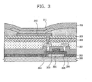
- FIG. 3 is a cross-sectional view of an OLED display device according to a third embodiment of the present invention.
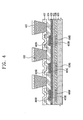
- FIG. 4 is a cross-sectional view of an OLED display device according to a fourth embodiment of the present invention.
- FIG. 1 is a cross-sectional view of an organic light emitting diode (OLED) display device according to a first embodiment of the present invention.
- the OLED display device is a bottom-emitting OLED display device which emits light toward a substrate.
- a substrate 100, a second refraction layer 101, and a first refraction layer 102 are sequentially disposed, and an organic light emitting diode including a first electrode 103, an organic layer 104 having an emission layer, and a second electrode 105 are disposed on the first refraction layer 102.
- a sealing member (not illustrated) may be further included over the second electrode 105.
- the substrate 100 is formed of a light-penetrating material.
- the substrate 100 may be formed of transparent glass, or transparent polymer material, e.g., polymethylmethacrylate (PMMA), polyaniline (PANI) or polyethylene terephthalate (PET).
- PMMA polymethylmethacrylate
- PANI polyaniline
- PET polyethylene terephthalate
- An amount of light emitted from the emission layer of the organic layer 104 is reflected at surfaces of the second refraction layer 101, the first refraction layer 102, and the second electrode 105. Reflection between surfaces of these layers induces optical resonance. Due to the optical resonance, the intensity of the light generated from the emission layer is amplified through the optical resonance. The amplified light transmits out of the display device, and thus light extraction efficiency improves.
- a refractive index n1 of the first refraction layer 102 is smaller than a refractive index n2 of the second refraction layer 101.
- the first refraction layer 102 is formed not exceeding 100 nm. If the thickness of the first refraction layer 102 is greater than 100 nm, there is almost no significant difference in light extraction efficiency and color reproducibility according to the change in thickness of the first refraction layer 102. Moreover, if the first refraction layer 102 is thicker, it absorbs the light emitted from the emission layer, which can have an adverse effect on light extraction. Accordingly, the first refraction layer 102 is preferably formed not exceeding 100 nm. The first refractive layer 102 also protects the second refraction layer 101 disposed under the first refractive layer 102 during patterning of the first electrode 103.
- the second refraction layer 101 may be formed to a thickness not exceeding 350 nm.
- the absorption of light in the second refraction layer 101 may increase.
- the second refraction layer 101 may be formed to a thickness of 20 nm to 100 nm, or 150 nm to 350 nm, and more particularly, 50 nm to 80 nm or 180 nm to 200 nm. In this range, the light extraction efficiency and the color reproducibility can be significantly increased as compared with other thickness ranges. In wavelengths ranging from about 400 nm to 800 nm, which includes wavelengths for red, green and blue colors, the light extraction efficiency and the color reproducibility increase even when the first and second refraction layers 102 and 101 are formed to have the same thickness.
- the first and second refraction layers 102 and 101 are formed of a transparent material.
- the first and second refraction layers 102 and 101 may be formed of niobium oxide (Nb 2 O 5 tantalum oxide (Ta 2 O 5 ), titanium oxide (Ti 2 O 5 ) silicon nitride (SixNy), silicon oxide (SiO 2 ), antimony oxide (Sb 2 O 3 ), aluminum oxide (Al 2 O 3 ), zirconium oxide (ZrO 2 ), magnesium oxide (MgO), hafnium dioxide (HfO 2 ) or synthetic polymer.
- niobium oxide Nb 2 O 5 tantalum oxide (Ta 2 O 5 )
- the materials are selectively mixed to make the refractive index n1 of the first refraction layer 102 smaller than the refractive index n2 of the second refraction layer 101.
- the materials for the first and second refraction layers 102 and 101 can be selected to have n1 ranging from 1.4 to less than 1.8 and to have n2 be 1.1 times of n1.
- n1 may be less than a refractive index of the first electrode 103.
- the first and second refraction layers 102 and 101 may be formed by a sol-gel, spin coating, spraying, roll coating, ion beam deposition, electron beam deposition, laser ablation, chemical vapor deposition (CVD) or sputtering method, and preferably by a sputtering method to ensure uniformity and stability in forming a large-sized layer.
- a third refraction layer which is the same layer as the first refraction layer 102, may be further disposed between the second refraction layer 101 and the substrate 100.
- a stacked structure of the first and second refraction layers 102 and 101 or a stacked structure of the first refraction layer 102, the second refraction layer 101 and the third refraction layer may be repeatedly formed.
- the first electrode 103 is disposed on the first refractive layer 102, and serves as a transmissive electrode, through which light is emitted.
- the first electrode 103 may function as an anode, and may be formed of indium tin oxide (ITO), indium zinc oxide (IZO), tin oxide (TO), zinc oxide (ZnO) or a transparent conductive material.
- the first electrode 103 may function as a cathode, and may be formed as a thin layer through which light can pass.
- the first electrode 103 can be made of a material such as conductive metals having a low work function, e.g., magnesium (Mg), calcium (Ca), aluminum (Al), silver (Ag) or an alloy thereof.
- the organic layer 104 includes an emission layer, and may further include at least one layer selected from: a hole injection layer, a hole transport layer, an electrode injection layer, an electrode transport layer, a hole blocking layer and an electron blocking layer.
- the material for forming the emission layer is not particularly limited, and it may be formed of any material selected from well-known host and dopant materials.
- the host material includes 4,4'-N,N'-dicarbazole-biphenyl (CBP), bis-(2-methyl-8-quinolinato)-4-phenylphenolate aluminum (BAlq), 2,9-dimethyl-4,7-diphenyl-1,10-phenanthroline (BCP), N,N'-dicarbazolyl-1,4-dimethene-benzene (DCB), rubrene, and 9,10-bis(2-naphthyl)antracene (AND).
- CBP 4,4'-N,N'-dicarbazole-biphenyl
- BAlq bis-(2-methyl-8-quinolinato)-4-phenylphenolate aluminum
- BCP 2,9-dimethyl-4,7-diphenyl-1,10-phenanthroline
- DCB N,N'-dicarbazolyl-1,4-dimethene-benzene
- rubrene and 9,10-bis(2-naphthyl)antracene
- the dopant material includes 4,4'-bis(2,2'-diphenylvinyl)-1,1'-biphenyl (DPVBi), distyrylamine derivatives, pyrene derivatives, perylene derivatives, distyrylbiphenyl (DSBP) derivatives, 10-(1,3-benzothiazole-2-yl)-1,1,7,7-tetramethyl-2,3,6,7-tetrahydro-1H,5H,11H-pyrano(2,3-f)pyrido(3,2,1-ij)quinoline-11-one (C545T), quinacridone derivatives, tris(2-phenylpyridine)iridium (Ir(PPy) 3 ), PQlr, Btp 2 Ir(acac), 4-(dicyanomethlylene)-2-tert-buthyl-6-(1,1,7,7-tetramethyljulorydyl-9-enyl)-4H-pyrane (DCJTB
- the hole injection layer may be formed of 4,4',4"-tris(3-methylphenylamino)triphenylamino (m-MTDATA), 1,3,5-trus[4-(3-methylphenylamino)phenyl]benzene (m-MTDATB), copper phthalocyanine (CuPc) or N,N'-di(4-(N,N'-diphenyl-amino)phenyl)-N,N'-diphenylbenzine (DNTPD), and the hole transport layer may be formed of N,N'-diphenyl-N,N'-bis(3-methylphenyl)-1,1'-biphenyl-4,4'-diamine (TPD), N,N'-di(naphthalene-1-yl)-N,N'-diphenyl benzidine ( ⁇ -NPD), or 4,4'-bis(1-naphthylphenylamino)biphenyl (NPB).
- the electron blocking layer may be formed of BAlq, BCP, CF-X, 3-(4-t-butylphenyl)-4-phenyl-5-(4-biphenyl)-1,2,4-triazole (TAZ) or spiro-TAZ, and the hole blocking layer 160 may be formed of 2-(4-biphenyl)-5-(4-tert-butylphenyl)-1,3,4-oxydiazole (PBD), spiro-PBD or TAZ.
- BAlq BAlq
- BCP 3-(4-t-butylphenyl)-4-phenyl-5-(4-biphenyl)-1,2,4-triazole (TAZ) or spiro-TAZ
- TAZ 2-(4-biphenyl)-5-(4-tert-butylphenyl)-1,3,4-oxydiazole
- TAZ 2-(4-biphenyl)-5-(4-tert-buty
- the electron transport layer may be formed of TAZ, PBD, spiro-PBD, Alq 3 , BAlq or SAlq, and the electron injection layer may be formed of LiF, a Ga complex, Liq or CsF.
- the organic layer 104 may be formed by thermal vacuum deposition, vapor deposition, spin coating, dip coating, doctor blading, inkjet printing or laser induced thermal imaging.
- the second electrode 105 is formed as a reflective layer.
- the second electrode 105 may function as a cathode, and may be formed as a thick layer to reflect light.
- the second electrode 105 may be formed of one material selected from the group consisting of conductive metals having a low work function, e.g., Mg, Ca, Al, Ag and an alloy thereof.
- the second electrode 105 may function as an anode, and may have a stacked structure having a reflective layer, which is formed of Ag, Al, chromium (Cr), Molybdenum (Mo), tungsten (W), titanium (Ti), gold (Au), palladium (Pd) or an alloy thereof, and a transparent layer, which is formed of ITO, IZO, TO or ZnO on the reflective layer.
- a reflective layer which is formed of Ag, Al, chromium (Cr), Molybdenum (Mo), tungsten (W), titanium (Ti), gold (Au), palladium (Pd) or an alloy thereof
- a transparent layer which is formed of ITO, IZO, TO or ZnO on the reflective layer.
- FIG. 2 is a cross-sectional view of an OLED display device according to a second embodiment of the present invention.
- the OLED display device is a top-emitting device, unlike the first embodiment. Except particular descriptions below, descriptions of the display device of the second embodiment will refer to those of the first embodiment.
- a first electrode 201 is disposed on a substrate 200.
- the first electrode 201 is formed as a reflective electrode.
- An organic layer 202 having an emission layer is disposed on the first electrode 201.
- a second electrode 203 is disposed on the organic layer 202.
- the second electrode 203 is formed as a transmissive electrode.
- a first refraction layer 204 is disposed on the second electrode 203, and a second refraction layer 205 is disposed on the first refraction layer 204.
- a refractive index n1 of the first refraction layer 204 is smaller than a refractive index n2 of the second refraction layer 205, and the first refraction layer 204 is formed to a thickness not exceeding 100 nm.
- the second refraction layer 205 may be formed to a thickness not exceeding 350 nm, preferably 20 nm to 100 nm or 150 nm to 350 nm, and more preferably 50 nm to 80 nm or 180 nm to 200 nm.
- FIG. 3 is a cross-sectional view of an OLED display device according to a third embodiment of the present invention.
- the OLED display device is an active matrix OLED display device including a thin film transistor electrically connected to a first electrode formed on a substrate, and is a bottom-emitting device. Except particular descriptions below, descriptions of the OLED display device of the third embodiment will refer to those of the first and second embodiments.
- a thin film transistor 306 including a semiconductor layer 301, a gate insulating layer 302, a gate electrode 303, and source and drain electrodes 304 and 305 is disposed on a substrate 300.
- a passivation layer 307 may be disposed on the source and drain electrodes 304 and 305.
- a second refraction layer 308 is disposed on the passivation layer 307, and a first refraction layer 309 is disposed on the second refraction layer 308.
- a first electrode 310 is disposed on the first refraction layer 309, and electrically connected to one of the source and drain electrodes 304 and 305 of the thin film transistor 306.
- the first electrode 310 is formed as a transmissive electrode.
- An organic layer 311 having an emission layer is disposed on the first electrode 310, and a second electrode 312 is disposed on the organic layer 311.
- the second electrode 312 is formed as a reflective electrode.
- the first electrode 310 is formed as a reflective electrode
- the second electrode 312 is formed as a transmissive electrode.
- the first refraction layer 309 is disposed over the second electrode 312, and the second refraction layer 308 is disposed on the first refraction layer 309.
- the first and second refraction layers 309 and the 308 may be disposed between the gate insulating layer 302 and the substrate 300.
- FIG. 4 is a cross-sectional view of an OLED display device according to a fourth embodiment of the present invention.
- the OLED display device is a full-color OLED display device having red, green and blue pixels, and is a bottom-emitting type. Except particular descriptions below, descriptions of the OLED display device will refer to those of the above embodiments.
- a substrate 400 having red (R), green (G) and blue (B) unit pixel regions is disposed.
- a second refraction layer 401 is disposed on the substrate 400, and a first refraction layer 402 is disposed on the second refraction layer 401.
- a refractive index n1 of the first refraction layer 402 is lower than a refractive index n2 of the second refraction layer 401, and the first refraction layer 402 is formed to a thickness greater than 0 and not exceeding 100 nm.
- the second refraction layer 401 may be formed to a thickness greater than 0 and not exceeding 350 nm, preferably, 20 nm to 100 nm or 150 nm to 350 nm, and more preferably 50 nm to 80 nm or 180 nm to 200 nm. In this range, light extraction efficiency and color reproducibility can be significantly increased as compared with other thickness ranges, and can also be increased even when the first and second refraction layers 402 and 401 have the same thickness in a wavelength range of red, green and blue light, which is a wavelength ranging from about 400 to 800nm. Therefore, the first and second refraction layers 402 and 401 do not need to be separately formed in each pixel, and thus the fabrication process can be simple.
- First electrodes 403R, 403G and 403B are disposed in respective unit pixel regions on the first refraction layer 402.
- the first electrodes 403R, 403G and 403B are transmissive electrodes.
- An insulating layer 404 defining pixel regions is disposed between the first electrodes 403R, 403G and 403B.
- Organic layers 405R, 405G and 405B having red, green and blue emission layers, respectively, are disposed on the first electrodes 403R, 403G and 403B, respectively.
- the organic layers 405R, 405G and 405B may be formed by vacuum deposition using a fine pitch mask, inkjet printing or laser induced thermal imaging.
- the organic layers 405R, 405G and 405B may be formed to the same thickness. However, to maximize resonance effect, the organic layer in a unit pixel region emitting light having a longer wavelength is preferably thicker than the organic layer in a unit pixel region emitting light having a shorter wavelength.
- Separators 406 may be disposed on the insulating layer 404.
- Second electrodes 407, each of which is isolated by the separators 406, are disposed on the organic layers 405R, 405G and 405B.
- the second electrodes 407 are reflective electrodes.
- the first electrodes 403R, 403G and 403B are formed as reflective electrodes, and the second electrodes 407 are formed as transmissive electrodes.
- the first refraction layer 402 is disposed over the second electrode 407, and the second refraction layer 401 is disposed on the first refraction layer 402.
- red, green and blue color filters 408R, 408G and 408B may be disposed in the respective unit pixel regions between the substrate 400 and the second refraction layer 401.
- the color filters 408R, 408G and 408B can further enhance color purity.
- a black matrix 409 may be disposed between the color filters.
- Sample OLED display devices were fabricated. Second refraction layers (Nb 2 O 5 , refractive index: 2.4) were formed to thicknesses listed in Table 1 on respective glass substrates.
- a first refraction layer (SiO 2 , refractive index: 1.45) was formed to a thickness of 30 nm on the second refraction layer.
- a first electrode which was made of ITO, was formed to a thickness of 50 nm on the first refraction layer.
- a hole injection layer was formed to a thickness of 75 nm using DNTPD on the first electrode, and a hole transport layer was formed to a thickness of 15 nm using NPB on the hole injection layer.
- a blue emission layer was formed to a thickness of 25 nm using AND as a host and EK8 (Kodak) as a dopant on the hole transport layer. Subsequently, an electron transport layer was formed to a thickness of 25 nm using Alq 3 on the blue emission layer, and an electron injection layer was formed to a thickness of 5 nm using LiF on the electron transport layer. A second electrode was formed to a thickness of 80 nm using Al on the electron injection layer.
- Tables 1 and 2 show color coordinates and brightness of the OLED display devices fabricated for Experimental examples 1 to 4 and 5 to 8.
- Tables 3 and 4 show color coordinates and brightness of the OLED display devices fabricated for Comparative examples 1 and 2 to 5.
- Comparative examples 2 to 5 when the second refraction layer was formed to a thickness of 120 nm, the brightness was increased, but the y value of the color coordinates was significantly increased compared to Comparative example 1. Thus, the increase in y value has a bad influence on the color reproducibility in spite of the increase in brightness.
- Second refraction layers (Nb 2 O 5 , refractive index: 2.4) were formed to thicknesses listed in Table 5 on respective glass substrates.
- a first refraction layer (SiO 2 , refractive index: 1.45) was formed to a thickness of 30 nm on the second refraction layer.
- the first electrode was formed to a thickness of 50 nm using ITO on the first refraction layer.
- Hole injection layers were formed to thicknesses of 145, 100 and 75 nm for red, green and blue pixels using DNTPD on the first electrode, respectively.
- a hole transport layer was formed to a thickness of 15 nm using NPB on the hole injection layers.
- a red emission layer was formed to a thickness of 45 nm using rubrene as a host and RD3 (Kodak) as a dopant
- a green emission layer was formed to a thickness of 45 nm using Alq 3 as a host and C545T as a dopant
- a blue emission layer was formed to a thickness of 25 nm using AND as a host and EK8 (Kodak) as a dopant on the hole transport layer.
- an electron transport layer was formed to a thickness of 25 nm using Alq 3 on the emission layers, and an electron injection layer was formed to a thickness of 5nm using LiF on the electron transport layer.
- a second electrode was formed to a thickness of 80nm using Al on the electron injection layer.
- Tables 5 to 8 show color coordinates and brightness for red, green and blue light in the OLED display devices according to Experimental examples 9 to 50.
- Table 9 shows color coordinates and brightness for red, green and blue light in the OLED display device according to Comparative example 6.
- the first refraction layer a low refraction layer
- the second refraction layer a high refraction layer
- an OLED display device can have enhanced light extraction efficiency and color coordinates, and thus can have improved color reproducibility with respect to red, green and blue light having a wavelength range from 400 to 800 nm.
- an OLED display device can have improved brightness and color coordinate characteristics in all emission wavelength ranges using a simple structure and process and thus enhanced light extraction efficiency and color reproducibility.
Landscapes
- Physics & Mathematics (AREA)
- Optics & Photonics (AREA)
- Electroluminescent Light Sources (AREA)
- Devices For Indicating Variable Information By Combining Individual Elements (AREA)
Abstract
Description
- The present invention relates to an organic light emitting diode (OLED) display device.
- Light efficiency for light emitting devices, particularly flat panel display devices such as OLED display devices, is classified into internal efficiency and external efficiency. The internal efficiency depends on photoelectric conversion efficiency of an organic light emitting material. In addition, the external efficiency, called light extraction efficiency, depends on a refractive index of each layer constituting an organic light emitting diode. The organic light emitting diode exhibits relatively lower light extraction efficiency, i.e., the external efficiency than other display devices such as cathode-ray tubes or PDPs, and thus there is much room for improvement in characteristics of the display device such as brightness, life span, etc.
- The biggest reason that the conventional organic light emitting diode has a lower light extraction efficiency than other display devices is because total reflection occurs at an interface between an ITO electrode layer having a high refractive index and a substrate having a low refractive index when light is emitted through the organic layer at more than a critical angle, thus preventing extraction of the light. Therefore, due to the total internal reflection at the interface in the organic light emitting diode, only about a quarter of the light actually generated from an organic emission layer can be extracted outside.
- An example of a conventional OLED display device for preventing a decrease in light extraction efficiency is disclosed in Japanese Patent Publication No.
63-314795 - To solve this problem of the OLED display device, an OLED display device having an optical microcavity is disclosed in Japanese Patent Application Laid-open Nos.
8-250786 8-213174 10-177896 - The present invention sets out to provide an organic light emitting diode (OLED) display device which can improve brightness and color coordinate characteristics in all emission wavelength ranges using a simple structure and process and thus enhance light extraction efficiency and color reproducibility.
- According to an embodiment of the present invention, an OLED display device includes a substrate, a first electrode disposed on the substrate, an organic layer disposed on the first electrode and including an emission layer, a second electrode disposed on the organic layer, and a first and a second refraction layers. A stack of the first and second refraction layers is disposed either between the first electrode and the substrate or on the second electrode. A refractive index of the first refraction layer is smaller than a refractive index of the second refraction layer. A thickness of the first refraction layer is no greater than 100 nm.
- The first electrode may be a transmissive electrode, and the second electrode may be a reflective electrode. In this case, the first refraction layer is disposed between the first electrode and the substrate, and the second refraction layer is disposed between the first refraction layer and the substrate.
- The first electrode may be a reflective electrode, and the second electrode may be a transmissive electrode. In this case, the first refraction layer is disposed on the second electrode, and the second refraction layer is disposed on the first refraction layer.
- The above and other features of the invention are set out in the appended claims.
- According to another embodiment of the present invention, an OLED display device includes a substrate including a plurality of unit pixel regions, a plurality of organic light emitting diodes disposed on the unit pixel regions of the substrate, and a first and a second refraction layers. Each of the organic light emitting diodes includes a first electrode, a second electrode, and an organic layer disposed between the first and the second electrodes. The organic layer has an emission layer. A stack of the first and second refraction layers is disposed either between the first electrode of each of the organic light emitting diodes and the substrate or on the second electrode of each of the organic light emitting diodes. A refractive index of the first refraction layer is smaller than a refractive index of the second refraction layer. A thickness of the first refraction layer is no greater than 100 nm.
- Additional aspects and/or advantages of the invention will be set forth in part in the description which follows and, in part, will be obvious from the description, or may be learned by practice of the invention.
- A more complete appreciation of the invention, and many of the attendant advantages thereof, will be readily apparent as the same becomes better understood by reference to the following detailed description when considered in conjunction with the accompanying drawings in which like reference symbols indicate the same or similar components, wherein:
-
FIG. 1 is a cross-sectional view of an organic light emitting diode (OLED) display device according to a first embodiment of the present invention; -
FIG. 2 is a cross-sectional view of an OLED display device according to a second embodiment of the present invention; -
FIG. 3 is a cross-sectional view of an OLED display device according to a third embodiment of the present invention; and -
FIG. 4 is a cross-sectional view of an OLED display device according to a fourth embodiment of the present invention. - Reference will now be made in detail to the present embodiments of the present invention, examples of which are illustrated in the accompanying drawings, wherein like reference numerals refer to the like elements throughout. The embodiments are described below in order to explain the present invention by referring to the figures.
-
FIG. 1 is a cross-sectional view of an organic light emitting diode (OLED) display device according to a first embodiment of the present invention. In the present embodiment, the OLED display device is a bottom-emitting OLED display device which emits light toward a substrate. - Referring to
FIG. 1 , asubstrate 100, asecond refraction layer 101, and afirst refraction layer 102 are sequentially disposed, and an organic light emitting diode including afirst electrode 103, anorganic layer 104 having an emission layer, and asecond electrode 105 are disposed on thefirst refraction layer 102. A sealing member (not illustrated) may be further included over thesecond electrode 105. - The
substrate 100 is formed of a light-penetrating material. Thesubstrate 100 may be formed of transparent glass, or transparent polymer material, e.g., polymethylmethacrylate (PMMA), polyaniline (PANI) or polyethylene terephthalate (PET). - An amount of light emitted from the emission layer of the
organic layer 104 is reflected at surfaces of thesecond refraction layer 101, thefirst refraction layer 102, and thesecond electrode 105. Reflection between surfaces of these layers induces optical resonance. Due to the optical resonance, the intensity of the light generated from the emission layer is amplified through the optical resonance. The amplified light transmits out of the display device, and thus light extraction efficiency improves. - In the present embodiment, a refractive index n1 of the
first refraction layer 102 is smaller than a refractive index n2 of thesecond refraction layer 101.
Thefirst refraction layer 102 is formed not exceeding 100 nm. If the thickness of thefirst refraction layer 102 is greater than 100 nm, there is almost no significant difference in light extraction efficiency and color reproducibility according to the change in thickness of thefirst refraction layer 102. Moreover, if thefirst refraction layer 102 is thicker, it absorbs the light emitted from the emission layer, which can have an adverse effect on light extraction. Accordingly, thefirst refraction layer 102 is preferably formed not exceeding 100 nm. The firstrefractive layer 102 also protects thesecond refraction layer 101 disposed under the firstrefractive layer 102 during patterning of thefirst electrode 103. - When the thickness of the
first refraction layer 102 is 100 nm or less, thesecond refraction layer 101 may be formed to a thickness not exceeding 350 nm. When thesecond refraction layer 101 has a thickness greater than 350 nm, the absorption of light in thesecond refraction layer 101 may increase. Preferably, thesecond refraction layer 101 may be formed to a thickness of 20 nm to 100 nm, or 150 nm to 350 nm, and more particularly, 50 nm to 80 nm or 180 nm to 200 nm. In this range, the light extraction efficiency and the color reproducibility can be significantly increased as compared with other thickness ranges. In wavelengths ranging from about 400 nm to 800 nm, which includes wavelengths for red, green and blue colors, the light extraction efficiency and the color reproducibility increase even when the first andsecond refraction layers - The first and second refraction layers 102 and 101 are formed of a transparent material. Specifically, the first and second refraction layers 102 and 101 may be formed of niobium oxide (Nb2O5 tantalum oxide (Ta2O5), titanium oxide (Ti2O5) silicon nitride (SixNy), silicon oxide (SiO2), antimony oxide (Sb2O3), aluminum oxide (Al2O3), zirconium oxide (ZrO2), magnesium oxide (MgO), hafnium dioxide (HfO2) or synthetic polymer. The materials are selectively mixed to make the refractive index n1 of the
first refraction layer 102 smaller than the refractive index n2 of thesecond refraction layer 101. Here, the materials for the first and second refraction layers 102 and 101 can be selected to have n1 ranging from 1.4 to less than 1.8 and to have n2 be 1.1 times of n1. In addition, n1 may be less than a refractive index of thefirst electrode 103. - The first and second refraction layers 102 and 101 may be formed by a sol-gel, spin coating, spraying, roll coating, ion beam deposition, electron beam deposition, laser ablation, chemical vapor deposition (CVD) or sputtering method, and preferably by a sputtering method to ensure uniformity and stability in forming a large-sized layer.
- Meanwhile, a third refraction layer, which is the same layer as the
first refraction layer 102, may be further disposed between thesecond refraction layer 101 and thesubstrate 100. Alternatively, a stacked structure of the first and second refraction layers 102 and 101 or a stacked structure of thefirst refraction layer 102, thesecond refraction layer 101 and the third refraction layer may be repeatedly formed. - Subsequently, the
first electrode 103 is disposed on the firstrefractive layer 102, and serves as a transmissive electrode, through which light is emitted. Thefirst electrode 103 may function as an anode, and may be formed of indium tin oxide (ITO), indium zinc oxide (IZO), tin oxide (TO), zinc oxide (ZnO) or a transparent conductive material. Alternatively, thefirst electrode 103 may function as a cathode, and may be formed as a thin layer through which light can pass. For example, thefirst electrode 103 can be made of a material such as conductive metals having a low work function, e.g., magnesium (Mg), calcium (Ca), aluminum (Al), silver (Ag) or an alloy thereof. - The
organic layer 104 includes an emission layer, and may further include at least one layer selected from: a hole injection layer, a hole transport layer, an electrode injection layer, an electrode transport layer, a hole blocking layer and an electron blocking layer. - The material for forming the emission layer is not particularly limited, and it may be formed of any material selected from well-known host and dopant materials.
- The host material includes 4,4'-N,N'-dicarbazole-biphenyl (CBP), bis-(2-methyl-8-quinolinato)-4-phenylphenolate aluminum (BAlq), 2,9-dimethyl-4,7-diphenyl-1,10-phenanthroline (BCP), N,N'-dicarbazolyl-1,4-dimethene-benzene (DCB), rubrene, and 9,10-bis(2-naphthyl)antracene (AND). The dopant material includes 4,4'-bis(2,2'-diphenylvinyl)-1,1'-biphenyl (DPVBi), distyrylamine derivatives, pyrene derivatives, perylene derivatives, distyrylbiphenyl (DSBP) derivatives, 10-(1,3-benzothiazole-2-yl)-1,1,7,7-tetramethyl-2,3,6,7-tetrahydro-1H,5H,11H-pyrano(2,3-f)pyrido(3,2,1-ij)quinoline-11-one (C545T), quinacridone derivatives, tris(2-phenylpyridine)iridium (Ir(PPy)3), PQlr, Btp2Ir(acac), 4-(dicyanomethlylene)-2-tert-buthyl-6-(1,1,7,7-tetramethyljulorydyl-9-enyl)-4H-pyrane (DCJTB), 4-(dicyanomethylene)-2-methyl-6-(p-dimethylaminostyryl)-4H-pyrane (DCM), 2,3,7,8,12,13,17,18-oxtaethyl-21 H,23H-porphirne-platinum complex (PtOEP), Ir(piq)2(acac), RD3(Kodak) and EK8(Kodak).
- The hole injection layer may be formed of 4,4',4"-tris(3-methylphenylamino)triphenylamino (m-MTDATA), 1,3,5-trus[4-(3-methylphenylamino)phenyl]benzene (m-MTDATB), copper phthalocyanine (CuPc) or N,N'-di(4-(N,N'-diphenyl-amino)phenyl)-N,N'-diphenylbenzine (DNTPD), and the hole transport layer may be formed of N,N'-diphenyl-N,N'-bis(3-methylphenyl)-1,1'-biphenyl-4,4'-diamine (TPD), N,N'-di(naphthalene-1-yl)-N,N'-diphenyl benzidine (α-NPD), or 4,4'-bis(1-naphthylphenylamino)biphenyl (NPB).
- The electron blocking layer may be formed of BAlq, BCP, CF-X, 3-(4-t-butylphenyl)-4-phenyl-5-(4-biphenyl)-1,2,4-triazole (TAZ) or spiro-TAZ, and the hole blocking layer 160 may be formed of 2-(4-biphenyl)-5-(4-tert-butylphenyl)-1,3,4-oxydiazole (PBD), spiro-PBD or TAZ.
- The electron transport layer may be formed of TAZ, PBD, spiro-PBD, Alq3, BAlq or SAlq, and the electron injection layer may be formed of LiF, a Ga complex, Liq or CsF.
- The
organic layer 104 may be formed by thermal vacuum deposition, vapor deposition, spin coating, dip coating, doctor blading, inkjet printing or laser induced thermal imaging. - The
second electrode 105 is formed as a reflective layer. Thesecond electrode 105 may function as a cathode, and may be formed as a thick layer to reflect light. Thesecond electrode 105 may be formed of one material selected from the group consisting of conductive metals having a low work function, e.g., Mg, Ca, Al, Ag and an alloy thereof. Alternatively, thesecond electrode 105 may function as an anode, and may have a stacked structure having a reflective layer, which is formed of Ag, Al, chromium (Cr), Molybdenum (Mo), tungsten (W), titanium (Ti), gold (Au), palladium (Pd) or an alloy thereof, and a transparent layer, which is formed of ITO, IZO, TO or ZnO on the reflective layer. -
FIG. 2 is a cross-sectional view of an OLED display device according to a second embodiment of the present invention. The OLED display device is a top-emitting device, unlike the first embodiment. Except particular descriptions below, descriptions of the display device of the second embodiment will refer to those of the first embodiment. - Referring to
FIG. 2 , afirst electrode 201 is disposed on asubstrate 200. Thefirst electrode 201 is formed as a reflective electrode. Anorganic layer 202 having an emission layer is disposed on thefirst electrode 201. Asecond electrode 203 is disposed on theorganic layer 202. Thesecond electrode 203 is formed as a transmissive electrode. - In the present embodiment, since light is emitted through the
second electrode 203, afirst refraction layer 204 is disposed on thesecond electrode 203, and asecond refraction layer 205 is disposed on thefirst refraction layer 204. Like the first embodiment, a refractive index n1 of thefirst refraction layer 204 is smaller than a refractive index n2 of thesecond refraction layer 205, and thefirst refraction layer 204 is formed to a thickness not exceeding 100 nm. Meanwhile, thesecond refraction layer 205 may be formed to a thickness not exceeding 350 nm, preferably 20 nm to 100 nm or 150 nm to 350 nm, and more preferably 50 nm to 80 nm or 180 nm to 200 nm. -
FIG. 3 is a cross-sectional view of an OLED display device according to a third embodiment of the present invention. The OLED display device is an active matrix OLED display device including a thin film transistor electrically connected to a first electrode formed on a substrate, and is a bottom-emitting device. Except particular descriptions below, descriptions of the OLED display device of the third embodiment will refer to those of the first and second embodiments. - Referring to
FIG. 3 , athin film transistor 306 including asemiconductor layer 301, agate insulating layer 302, agate electrode 303, and source and drainelectrodes substrate 300. Apassivation layer 307 may be disposed on the source and drainelectrodes - A
second refraction layer 308 is disposed on thepassivation layer 307, and afirst refraction layer 309 is disposed on thesecond refraction layer 308. - A
first electrode 310 is disposed on thefirst refraction layer 309, and electrically connected to one of the source and drainelectrodes thin film transistor 306. Thefirst electrode 310 is formed as a transmissive electrode. - An
organic layer 311 having an emission layer is disposed on thefirst electrode 310, and asecond electrode 312 is disposed on theorganic layer 311. Thesecond electrode 312 is formed as a reflective electrode. - Meanwhile, in the top-emitting active-matrix OLED display device, the
first electrode 310 is formed as a reflective electrode, and thesecond electrode 312 is formed as a transmissive electrode. Thefirst refraction layer 309 is disposed over thesecond electrode 312, and thesecond refraction layer 308 is disposed on thefirst refraction layer 309. Alternatively, the first and second refraction layers 309 and the 308 may be disposed between thegate insulating layer 302 and thesubstrate 300. -
FIG. 4 is a cross-sectional view of an OLED display device according to a fourth embodiment of the present invention. The OLED display device is a full-color OLED display device having red, green and blue pixels, and is a bottom-emitting type. Except particular descriptions below, descriptions of the OLED display device will refer to those of the above embodiments. - Referring to
FIG. 4 , asubstrate 400 having red (R), green (G) and blue (B) unit pixel regions is disposed. Asecond refraction layer 401 is disposed on thesubstrate 400, and afirst refraction layer 402 is disposed on thesecond refraction layer 401. Like the above embodiments, a refractive index n1 of thefirst refraction layer 402 is lower than a refractive index n2 of thesecond refraction layer 401, and thefirst refraction layer 402 is formed to a thickness greater than 0 and not exceeding 100 nm. Meanwhile, thesecond refraction layer 401 may be formed to a thickness greater than 0 and not exceeding 350 nm, preferably, 20 nm to 100 nm or 150 nm to 350 nm, and more preferably 50 nm to 80 nm or 180 nm to 200 nm. In this range, light extraction efficiency and color reproducibility can be significantly increased as compared with other thickness ranges, and can also be increased even when the first and second refraction layers 402 and 401 have the same thickness in a wavelength range of red, green and blue light, which is a wavelength ranging from about 400 to 800nm. Therefore, the first and second refraction layers 402 and 401 do not need to be separately formed in each pixel, and thus the fabrication process can be simple. -
First electrodes first refraction layer 402. Thefirst electrodes layer 404 defining pixel regions is disposed between thefirst electrodes -
Organic layers first electrodes organic layers organic layers -
Separators 406 may be disposed on the insulatinglayer 404.Second electrodes 407, each of which is isolated by theseparators 406, are disposed on theorganic layers second electrodes 407 are reflective electrodes. - Meanwhile, in the top-emission active-matrix OLED display device, the
first electrodes second electrodes 407 are formed as transmissive electrodes. In addition, thefirst refraction layer 402 is disposed over thesecond electrode 407, and thesecond refraction layer 401 is disposed on thefirst refraction layer 402. - Moreover, red, green and
blue color filters substrate 400 and thesecond refraction layer 401. The color filters 408R, 408G and 408B can further enhance color purity. Ablack matrix 409 may be disposed between the color filters. - Hereinafter, preferable experimental examples will be described to aid in understanding of the present invention. However, it should be understood that the experimental examples described below are provided to aid in understanding of the present invention, and not to limit the present invention.
- Experimental examples 1 to 4
- Sample OLED display devices were fabricated. Second refraction layers (Nb2O5, refractive index: 2.4) were formed to thicknesses listed in Table 1 on respective glass substrates. A first refraction layer (SiO2, refractive index: 1.45) was formed to a thickness of 30 nm on the second refraction layer. A first electrode, which was made of ITO, was formed to a thickness of 50 nm on the first refraction layer. A hole injection layer was formed to a thickness of 75 nm using DNTPD on the first electrode, and a hole transport layer was formed to a thickness of 15 nm using NPB on the hole injection layer. A blue emission layer was formed to a thickness of 25 nm using AND as a host and EK8 (Kodak) as a dopant on the hole transport layer. Subsequently, an electron transport layer was formed to a thickness of 25 nm using Alq3 on the blue emission layer, and an electron injection layer was formed to a thickness of 5 nm using LiF on the electron transport layer. A second electrode was formed to a thickness of 80 nm using Al on the electron injection layer.
- Experimental examples 5 to 8
- Except that a first refraction layer was formed to a thickness of 90 nm, other sample OLED display devices were fabricated with the same conditions as in Experimental examples 1 to 4.
- Comparative example 1
- Compared with Experimental example 1, first and second refraction layers were not formed.
- Comparative examples 2 to 5
- Except that a first refraction layer was formed to a thickness of 120 nm, the samples were fabricated with the same conditions as in Experimental examples 1 to 4.
- Tables 1 and 2 show color coordinates and brightness of the OLED display devices fabricated for Experimental examples 1 to 4 and 5 to 8. Tables 3 and 4 show color coordinates and brightness of the OLED display devices fabricated for Comparative examples 1 and 2 to 5.
-
Table 1 Thickness of
Nb2O5 (nm)X y Brightness E. example 1 50 0.149 0.093 62.7 E. example 2 80 0.134 0.140 89.7 E. example 3 180 0.134 0.145 82.3 E. example 4 230 0.154 0.131 86.6 -
Table 2 Thickness of
Nb2O5 (nm)X y Brightness E. example 5 50 0.124 0.141 96.5 E. example 6 80 0.125 0.209 120.2 E. example 7 180 0.127 0.179 111.1 E. example 8 230 0.137 0.142 96.6 -
Table 3 x Y Brightness C. example 1 0.145 0.202 112.5 -
Table 4 Thickness of
Nb2O5 (nm)X y Brightness C. example 2 50 0.141 0.403 153.4 C. example 3 80 0.165 0.268 130.9 C. example 4 180 0.137 0.263 137.6 C. example 5 230 0.140 0.344 134.8 - Referring to Tables 1 to 4, in Experimental examples 1 to 4 and 5 to 8, comparing the first refraction layers having thicknesses of 30 nm and 90 nm, the brightness was slightly decreased at 30 nm, but the y value of the color coordinates was significantly decreased compared to Comparative example 1, or there was no significant difference in y value and the brightness was increased. For blue, although the brightness was slightly decreased, the color reproducibility was increased as the y value is decreased. Therefore, when the first refraction layer was formed to a thickness of 100 nm or less, the color reproducibility and the light extraction efficiency were increased. On the other hand, in Comparative examples 2 to 5, when the second refraction layer was formed to a thickness of 120 nm, the brightness was increased, but the y value of the color coordinates was significantly increased compared to Comparative example 1. Thus, the increase in y value has a bad influence on the color reproducibility in spite of the increase in brightness.
- Experimental examples 9 to 20
- Second refraction layers (Nb2O5, refractive index: 2.4) were formed to thicknesses listed in Table 5 on respective glass substrates. A first refraction layer (SiO2, refractive index: 1.45) was formed to a thickness of 30 nm on the second refraction layer. The first electrode was formed to a thickness of 50 nm using ITO on the first refraction layer. Hole injection layers were formed to thicknesses of 145, 100 and 75 nm for red, green and blue pixels using DNTPD on the first electrode, respectively. A hole transport layer was formed to a thickness of 15 nm using NPB on the hole injection layers. A red emission layer was formed to a thickness of 45 nm using rubrene as a host and RD3 (Kodak) as a dopant, a green emission layer was formed to a thickness of 45 nm using Alq3 as a host and C545T as a dopant, and a blue emission layer was formed to a thickness of 25 nm using AND as a host and EK8 (Kodak) as a dopant on the hole transport layer. Subsequently, an electron transport layer was formed to a thickness of 25 nm using Alq3 on the emission layers, and an electron injection layer was formed to a thickness of 5nm using LiF on the electron transport layer. A second electrode was formed to a thickness of 80nm using Al on the electron injection layer.
- Experimental examples 21 to 32
- Except that Ta2O5 having a refractive index of 2.1 as a second refraction layer was used, the experiments were performed under the same conditions as in Experimental examples 9 to 20.
- Experimental examples 33 to 44
- Except that TiO2 having a refractive index of 2.3 as a second refraction layer was used, the experiments were performed under the same conditions as in Experimental examples 9 to 20.
- Experimental examples 45 to 50
- Except that SiN having a refractive index of 1.8 as a second refraction layer was formed to a thickness listed in Table 8, the experiments were performed under the same conditions as in Experimental example 9.
- Comparative example 6
- Except that first and second refraction layers were not formed, the experiment was performed under the same conditions as in Experimental example 9.
- Tables 5 to 8 show color coordinates and brightness for red, green and blue light in the OLED display devices according to Experimental examples 9 to 50. Table 9 shows color coordinates and brightness for red, green and blue light in the OLED display device according to Comparative example 6.
-
Table 5 Red Green blue Thickness of
Nb2O5 (nm)x y Brightness x y Brightness x y Brightness E.example 9 20 0.662 0.338 131.2 0.265 0.671 132.2 0.145 0.124 87.8 E.example 10 50 0.661 0.339 204.8 0.264 0.693 177.5 0.129 0.131 95.4 E.example 11 80 0.670 0.329 195.5 0.328 0.642 159.9 0.123 0.213 124.4 E.example 12 100 0.673 0.327 148.3 0.342 0.619 135.0 0.141 0.187 121.0 E.example 13 120 0.670 0.333 122.4 0.302 0.641 130.3 0.147 0.132 101.1 E.example 14 150 0.660 0.340 139.7 0.256 0.695 162.6 0.129 0.144 95.0 E.example 15 180 0.661 0.338 207.2 0.300 0.667 162.8 0.125 0.188 113.8 E.example 16 200 0.668 0.332 204.5 0.329 0.635 147.7 0.138 0.166 118.7 E.example 17 230 0.673 0.327 143.8 0.306 0.640 140.2 0.141 0.145 102.8 E.example 18 270 0.662 0.338 133.3 0.273 0.686 160.5 0.129 0.168 103.6 E.example 19 300 0.660 0.340 192.4 0.308 0.656 151.8 0.135 0.157 114.3 E.example 20 350 0.673 0.327 155.8 0.292 0.658 151.6 0.135 0.162 102.1 -
Table 6 Red Green blue Thickness of
Ta2O5 (nm)x y Brightness x y Brightness x y Brightness E.example 21 20 0.664 0.336 124.4 0.286 0.656 124.7 0.145 0.152 97.1 E.example 22 50 0.662 0.338 165.8 0.269 0.680 157.7 0.135 0.135 97.6 E.example 23 80 0.667 0.333 186.0 0.310 0.655 159.5 0.126 0.193 118.0 E.example 24 100 0.670 0.329 162.1 0.334 0.631 142.7 0.132 0.215 124.8 E.example 25 120 0.667 0.333 119.1 0.334 0.623 127.5 0.144 0.185 117.2 E.example 26 150 0.661 0.338 142.1 0.288 0.655 132.2 0.144 0.140 100.8 E.example 27 180 0.662 0.338 171.0 0.274 0.680 154.3 0.130 0.165 103.8 E.example 28 200 0.668 0.332 179.2 0.295 0.667 155.7 0.127 0.193 112.7 E.example 29 230 0.673 0.327 143.8 0.328 0.634 140.7 0.138 0.181 118.7 E.example 30 270 0.671 0.329 131.9 0.305 0.641 134.0 0.141 0.155 105.9 E.example 31 300 0.666 0.334 122.6 0.279 0.673 148.3 0.133 0.175 105.0 E.example 32 350 0.662 0.338 174.1 0.315 0.646 142.8 0.138 0.168 115.7 -
Table 7 Red Green blue Thickness of TiO2 (nm) x y Brightness x y Brightness x y Brightness E.example 33 20 0.662 0.338 129.2 0.270 0.667 130.4 0.145 0.129 90.0 E.example 34 50 0.661 0.339 193.8 0.264 0.691 173.6 0.130 0.131 95.9 E.example 35 80 0.669 0.330 195.9 0.324 0.646 160.7 0.123 0.210 123.0 E.example 36 100 0.673 0.327 153.2 0.342 0.621 137.1 0.139 0.194 122.9 E.example 37 120 0.671 0.329 125.0 0.313 0.633 128.2 0.147 0.141 105.6 E.example 38 150 0.662 0.338 130.4 0.259 0.688 155.8 0.133 0.142 94.3 E.example 39 180 0.660 0.340 188.9 0.291 0.672 163.2 0.124 0.187 111.1 E.example 40 200 0.666 0.334 205.3 0.322 0.644 150.9 0.135 0.174 118.8 E.example 41 230 0.673 0.327 155.9 0.319 0.630 137.1 0.142 0.149 107.9 E.example 42 270 0.666 0.334 124.9 0.272 0.683 156.9 0.130 0.167 102.0 E.example 43 300 0.659 0.341 165.2 0.298 0.666 153.7 0.134 0.160 112.7 E.example 44 350 0.671 0.329 175.3 0.305 0.644 145.6 0.136 0.165 105.2 -
Table 8 Red Green Blue Thickness of SiN (nm) x y Brightness x y Brightness x y Brightness E.example 45 50 0.664 0.336 141.1 0.285 0.663 139.1 0.140 0.152 102.1 E.example 46 100 0.668 0.320 155.8 0.320 0.641 141.9 0.133 0.206 102.7 E.example 47 150 0.669 0.331 121.6 0.320 0.631 121.9 0.146 0.176 111.6 E.example 48 200 0.664 0.336 129.7 0.287 0.664 139.9 0.136 0.171 107.2 E.example 49 300 0.670 0.330 130.4 0.317 0.633 126.3 0.144 0.168 110.7 E.example 50 350 0.665 0.335 123.0 0.292 0.662 139.2 0.135 0.188 110.1 -
Table 9 red Green Blue x Y Brightness X Y Brightness x Y Brightness 0.667 0.334 114.2 0.317 0.635 115.3 0.145 0.202 112.5 - Referring to Tables 5 to 9, in Experimental examples 9 to 50, when the thickness of the first refraction layer was fixed to 60 nm, and the thickness of the second refraction layer was changed within a range greater than 0 to not exceeding 350 nm, the brightness of red and green light was increased in every range as compared with Comparative example 6, and the brightness of blue light was decreased in y value of color coordinates or increased in brightness. Particularly, when the second refraction layer was formed to a thickness of 20 to 100 nm or 150 to 350 nm, and preferably 50 to 80 nm or 180 to 200 nm, the increase in brightness was greater than that in other ranges of thickness.
- As described above, when the first refraction layer, a low refraction layer, is formed to a thickness of 100 nm or less, the light extraction efficiency and color reproducibility can be improved. In addition, when the second refraction layer, a high refraction layer, is formed to a thickness greater than 0 and not exceeding 350 nm, preferably 20 to 100 nm or 150 to 350 nm, and more particularly 50 to 80 nm or 180 to 200 nm, and even formed to the same thickness as the first refraction layer, an OLED display device can have enhanced light extraction efficiency and color coordinates, and thus can have improved color reproducibility with respect to red, green and blue light having a wavelength range from 400 to 800 nm.
- According to the present invention, as thicknesses of first and second refraction layers disposed between an electrode and a transparent substrate are controlled, an OLED display device can have improved brightness and color coordinate characteristics in all emission wavelength ranges using a simple structure and process and thus enhanced light extraction efficiency and color reproducibility.
- Although a few embodiments of the present invention have been shown and described, it would be appreciated by those skilled in the art that changes may be made in this embodiment without departing from the principles of the invention, the scope of which is defined in the claims and their equivalents.
Claims (16)
- An organic light emitting diode (OLED) display device, comprising:a substrate;a first electrode disposed on the substrate;an organic layer disposed on the first electrode and including an emission layer;a second electrode disposed on the organic layer; andfirst and a second refraction layer, disposed either between the first electrode and the substrate or on the second electrode; wherein a refractive index of the first refraction layer is smaller than a refractive index of the second refraction layer, and the first refraction layer has a thickness of 100 nm or less.
- An OLED display device according to claim 1, wherein the second refraction layer has a thickness of 350 nm or less.
- An OLED display device according to claim 2, wherein the thickness of the second refraction layer is either from 20 nm to 100 nm, or from 150 nm to 350 nm.
- An OLED display device according to claim 3, wherein the thickness of the second refraction layer is either from 50 nm to 80 nm, or from 180 nm to 200 nm.
- An OLED display device according to according to any preceding claim, wherein the refractive index of the second refraction layer is 1.1 times greater than the refractive index of the first refraction layer.
- An OLED display device according to any preceding claim, wherein: the first and second refraction layers are disposed between the first electrode and the substrate, and the refractive index of the first refraction layer is smaller than a refractive index of the first electrode; or the first and second refraction layers are disposed on the second electrode, and the refractive index of the first refraction layer is smaller than a refractive index of the second electrode.
- An OLED display device according to any preceding claim, wherein the refractive index of the first refraction layer is from 1.4 to 1.8.
- An OLED display device according to any preceding, wherein each of the first and second refraction layers includes niobium oxide (Nb2O5), tantalum oxide (Ta2O5) titanium oxide (Ti2O5), silicon nitride (SixNy), silicon oxide (SiO2), antimony oxide (Sb2O3), aluminum oxide (Al2O3), zirconium oxide (ZrO2), magnesium oxide (MgO), Hafnium oxide (HfO2) or synthetic polymer.
- An OLED display device according according to any preceding claim, wherein the first electrode is a transmissive electrode, the second electrode is a reflective electrode, the first refraction layer is disposed between the first electrode and the substrate, and the second refraction layer is disposed between the first refraction layer and the substrate.
- An OLED display device according to one of claims 1 to 8, wherein the first electrode is a reflective electrode, the second electrode is a transmissive electrode, the first refraction layer is disposed on the second electrode, and the second refraction layer is disposed on the first refraction layer.
- An OLED display device according to any preceding claim, wherein the first refraction layer of and the second refraction layer have substantially the same thicknesses.
- An OLED display device according to any preceding claim:wherein the substrate includes a plurality of unit pixel regions;a plurality of organic light emitting diodes are disposed on the unit pixel regions of the substrate; and the said first electrode, second electrode, organic layer and first and a second refraction layers, together at least partially define one of the said organic light emitting diodes, each of the other said organic light emitting diodes being correspondingly configured.
- An OLED display device according to any preceding claim, further comprising:a third refraction layer either disposed between the second refraction layer and the substrate, if the first and second refraction layers are disposed between the first electrode and the substrate, or disposed on the second refraction layer, if the first and second refraction layers are disposed on the second electrode; wherein the third refraction layer has a refractive index that is the same as the refractive index of the first refraction layer, and a thickness that is the same as the thickness of the first refraction layer.
- An OLED display device according to any preceding claim, wherein one organic layer emitting light having a longer wavelength is thicker than another organic layer emitting light having a shorter wavelength.
- An OLED display device according to any preceding claim, further comprising:a color filter disposed between the second refraction layer and the substrate, if the first and second refraction layers are disposed between the first electrode and the substrate.
- An OLED display device according to one of claims 1 to 14, further comprising:a color filter disposed on the second refraction layer, if the first and second refraction layers are disposed on the second electrode.
Applications Claiming Priority (1)
| Application Number | Priority Date | Filing Date | Title |
|---|---|---|---|
| KR1020080053339A KR100953658B1 (en) | 2008-06-05 | 2008-06-05 | Organic light emitting display |
Publications (2)
| Publication Number | Publication Date |
|---|---|
| EP2131411A1 true EP2131411A1 (en) | 2009-12-09 |
| EP2131411B1 EP2131411B1 (en) | 2016-01-13 |
Family
ID=40997874
Family Applications (1)
| Application Number | Title | Priority Date | Filing Date |
|---|---|---|---|
| EP09251503.0A Not-in-force EP2131411B1 (en) | 2008-06-05 | 2009-06-05 | Organic light emitting diode display device |
Country Status (5)
| Country | Link |
|---|---|
| US (1) | US8154197B2 (en) |
| EP (1) | EP2131411B1 (en) |
| JP (1) | JP5410842B2 (en) |
| KR (1) | KR100953658B1 (en) |
| CN (1) | CN101599536B (en) |
Cited By (2)
| Publication number | Priority date | Publication date | Assignee | Title |
|---|---|---|---|---|
| EP2738830A3 (en) * | 2012-11-29 | 2016-08-17 | Samsung Display Co., Ltd. | Organic light-emitting display device and method of manufacturing the same |
| EP3242342A4 (en) * | 2014-12-31 | 2018-02-07 | Beijing Visionox Technology Co., Ltd. | Oled device having optical resonance layer and preparation method therefor, and display |
Families Citing this family (57)
| Publication number | Priority date | Publication date | Assignee | Title |
|---|---|---|---|---|
| JP5328726B2 (en) | 2009-08-25 | 2013-10-30 | 三星ディスプレイ株式會社 | Thin film deposition apparatus and organic light emitting display device manufacturing method using the same |
| JP5677785B2 (en) | 2009-08-27 | 2015-02-25 | 三星ディスプレイ株式會社Samsung Display Co.,Ltd. | Thin film deposition apparatus and organic light emitting display device manufacturing method using the same |
| US8876975B2 (en) | 2009-10-19 | 2014-11-04 | Samsung Display Co., Ltd. | Thin film deposition apparatus |
| KR20110057673A (en) * | 2009-11-24 | 2011-06-01 | 삼성모바일디스플레이주식회사 | Organic light emitting device |
| KR20110058126A (en) * | 2009-11-25 | 2011-06-01 | 삼성모바일디스플레이주식회사 | Organic light emitting display |
| KR101084184B1 (en) | 2010-01-11 | 2011-11-17 | 삼성모바일디스플레이주식회사 | Thin film deposition apparatus |
| KR101174875B1 (en) | 2010-01-14 | 2012-08-17 | 삼성디스플레이 주식회사 | Apparatus for thin layer deposition, method for manufacturing of organic light emitting display apparatus using the same, and organic light emitting display apparatus manufactured by the method |
| KR101193186B1 (en) | 2010-02-01 | 2012-10-19 | 삼성디스플레이 주식회사 | Apparatus for thin layer deposition, method for manufacturing of organic light emitting display apparatus using the same, and organic light emitting display apparatus manufactured by the method |
| KR101156441B1 (en) | 2010-03-11 | 2012-06-18 | 삼성모바일디스플레이주식회사 | Apparatus for thin layer deposition |
| JP5567369B2 (en) * | 2010-03-26 | 2014-08-06 | ユー・ディー・シー アイルランド リミテッド | Organic electroluminescent device and organic electroluminescent display using the same |
| KR101054983B1 (en) * | 2010-03-29 | 2011-08-05 | 엘지이노텍 주식회사 | Light emitting device, manufacturing method, light emitting device package |
| KR101202348B1 (en) | 2010-04-06 | 2012-11-16 | 삼성디스플레이 주식회사 | Apparatus for thin layer deposition and method for manufacturing of organic light emitting display apparatus using the same |
| US8894458B2 (en) | 2010-04-28 | 2014-11-25 | Samsung Display Co., Ltd. | Thin film deposition apparatus, method of manufacturing organic light-emitting display device by using the apparatus, and organic light-emitting display device manufactured by using the method |
| KR101223723B1 (en) | 2010-07-07 | 2013-01-18 | 삼성디스플레이 주식회사 | Apparatus for thin layer deposition, method for manufacturing of organic light emitting display apparatus using the same, and organic light emitting display apparatus manufactured by the method |
| KR20120042143A (en) * | 2010-10-22 | 2012-05-03 | 삼성모바일디스플레이주식회사 | Organinc light emitting display device and manufacturing method for the same |
| KR101723506B1 (en) | 2010-10-22 | 2017-04-19 | 삼성디스플레이 주식회사 | Apparatus for organic layer deposition and method for manufacturing of organic light emitting display apparatus using the same |
| KR101738531B1 (en) * | 2010-10-22 | 2017-05-23 | 삼성디스플레이 주식회사 | Method for manufacturing of organic light emitting display apparatus, and organic light emitting display apparatus manufactured by the method |
| KR20120045865A (en) | 2010-11-01 | 2012-05-09 | 삼성모바일디스플레이주식회사 | Apparatus for organic layer deposition |
| KR20120065789A (en) | 2010-12-13 | 2012-06-21 | 삼성모바일디스플레이주식회사 | Apparatus for organic layer deposition |
| US8476622B2 (en) * | 2011-01-05 | 2013-07-02 | Electronics And Telecommunications Research Institute | Active matrix organic light emitting diode |
| KR101760897B1 (en) | 2011-01-12 | 2017-07-25 | 삼성디스플레이 주식회사 | Deposition source and apparatus for organic layer deposition having the same |
| KR101852517B1 (en) | 2011-05-25 | 2018-04-27 | 삼성디스플레이 주식회사 | Apparatus for organic layer deposition and method for manufacturing of organic light emitting display apparatus using the same |
| KR101840654B1 (en) | 2011-05-25 | 2018-03-22 | 삼성디스플레이 주식회사 | Apparatus for organic layer deposition and method for manufacturing of organic light emitting display apparatus using the same |
| KR101857249B1 (en) | 2011-05-27 | 2018-05-14 | 삼성디스플레이 주식회사 | Patterning slit sheet assembly, apparatus for organic layer deposition, method for manufacturing organic light emitting display apparatus and organic light emitting display apparatus |
| KR101893355B1 (en) | 2011-06-30 | 2018-10-05 | 삼성디스플레이 주식회사 | Light emitting device and organic light emitting display apparatus comprising the same |
| KR101826068B1 (en) | 2011-07-04 | 2018-02-07 | 삼성디스플레이 주식회사 | Apparatus for thin layer deposition |
| KR101421169B1 (en) | 2011-07-15 | 2014-07-24 | 엘지디스플레이 주식회사 | Organic light emitting display device |
| KR101317276B1 (en) * | 2011-07-25 | 2013-10-14 | 포항공과대학교 산학협력단 | Substrate for organic light emitting diodes and manufacturing method thereof |
| JP6223341B2 (en) | 2011-08-31 | 2017-11-01 | オーエルイーディーワークス ゲーエムベーハーOLEDWorks GmbH | Output coupling device and light source |
| JP6379347B2 (en) * | 2011-11-02 | 2018-08-29 | 株式会社Joled | Organic light emitting panel and method for manufacturing the same |
| CN103178077B (en) * | 2011-12-21 | 2016-08-24 | 昆山工研院新型平板显示技术中心有限公司 | Organic elctroluminescent device and method for packing thereof |
| CN102709484A (en) * | 2012-06-03 | 2012-10-03 | 南京师范大学 | White light organic electroluminescent device and preparation method of white light organic electroluminescent device |
| KR102013315B1 (en) | 2012-07-10 | 2019-08-23 | 삼성디스플레이 주식회사 | Method for manufacturing of organic light emitting display apparatus and organic light emitting display apparatus manufactured by the method |
| KR101632298B1 (en) | 2012-07-16 | 2016-06-22 | 삼성디스플레이 주식회사 | Flat panel display device and manufacturing method thereof |
| KR101444777B1 (en) * | 2012-08-10 | 2014-09-26 | 엘지디스플레이 주식회사 | Organic light emitting diode display device and method of fabricating the same |
| KR102051103B1 (en) * | 2012-11-07 | 2019-12-03 | 삼성디스플레이 주식회사 | Organic light emitting diode display |
| CN104009178A (en) * | 2013-02-26 | 2014-08-27 | 海洋王照明科技股份有限公司 | Organic electroluminescent device and preparation method |
| KR20140119266A (en) * | 2013-03-28 | 2014-10-10 | 삼성디스플레이 주식회사 | Organic light emitting display device and manufacturing method thereof |
| KR20150005379A (en) | 2013-07-05 | 2015-01-14 | 삼성디스플레이 주식회사 | Organic light emitting diode display |
| CN103346269B (en) * | 2013-07-15 | 2016-03-09 | 广州新视界光电科技有限公司 | A kind of semitransparent electrode and there is the organic electroluminescence device of this semitransparent electrode |
| KR20150056375A (en) * | 2013-11-15 | 2015-05-26 | 삼성디스플레이 주식회사 | Organic light-emitting display apparatus |
| CN103972266B (en) * | 2014-04-16 | 2017-06-09 | 京东方科技集团股份有限公司 | A kind of organic EL display panel and display device |
| KR102296915B1 (en) | 2014-07-30 | 2021-09-02 | 삼성디스플레이 주식회사 | organic light emitting diode display |
| CN105825162B (en) * | 2015-01-09 | 2019-04-12 | 群创光电股份有限公司 | electronic device |
| CN104851988B (en) * | 2015-05-22 | 2018-03-30 | 京东方科技集团股份有限公司 | Organic light emitting display and preparation method thereof and display device |
| CN106920899A (en) * | 2016-04-26 | 2017-07-04 | 广东聚华印刷显示技术有限公司 | Organic electroluminescence device and preparation method thereof |
| JP2018006212A (en) * | 2016-07-05 | 2018-01-11 | 株式会社ジャパンディスプレイ | Display device |
| US11594698B2 (en) | 2016-08-23 | 2023-02-28 | Samsung Electronics Co., Ltd. | Electric device and display device comprising quantum dots with improved luminous efficiency |
| KR102649300B1 (en) | 2016-08-23 | 2024-03-18 | 삼성전자주식회사 | Electric device, and display device comprising the same |
| KR102769205B1 (en) * | 2016-12-16 | 2025-02-20 | 엘지디스플레이 주식회사 | Organic light emitting display |
| KR102783331B1 (en) * | 2017-02-02 | 2025-03-20 | 삼성디스플레이 주식회사 | Organic light emitting display device |
| CN108376696B (en) * | 2017-09-30 | 2020-08-25 | 云谷(固安)科技有限公司 | Terminals and Displays |
| KR102418609B1 (en) * | 2017-11-16 | 2022-07-08 | 삼성디스플레이 주식회사 | Display device |
| KR102218086B1 (en) * | 2019-03-21 | 2021-02-18 | 한국건설생활환경시험연구원 | Color solar module for bipv and manufacturing method thereof |
| KR102110471B1 (en) * | 2019-11-26 | 2020-05-14 | 삼성디스플레이 주식회사 | Organic light emitting diode display |
| CN110911588B (en) * | 2019-12-10 | 2022-04-05 | 京东方科技集团股份有限公司 | An electroluminescent display device, display panel and display device |
| US12339477B2 (en) * | 2020-05-26 | 2025-06-24 | Lawrence Livermore National Security, Llc | Amorphous or nanocrystalline molybdenum nitride and silicon nitride multilayers |
Citations (10)
| Publication number | Priority date | Publication date | Assignee | Title |
|---|---|---|---|---|
| JPS63314795A (en) | 1987-06-18 | 1988-12-22 | Komatsu Ltd | Film type el element |
| JPH08213174A (en) | 1992-09-22 | 1996-08-20 | Hitachi Ltd | Organic light emitting device and its substrate |
| JPH08250786A (en) | 1995-01-10 | 1996-09-27 | Hitachi Ltd | Light emitting device having multiple resonance structure |
| JPH10177896A (en) | 1998-01-05 | 1998-06-30 | Hitachi Ltd | Organic light emitting device |
| JP2003077680A (en) * | 2001-09-06 | 2003-03-14 | Konica Corp | Organic electroluminescent element and display device |
| WO2004077519A2 (en) * | 2003-02-27 | 2004-09-10 | Mukundan Narasimhan | Dielectric barrier layer films |
| EP1480281A2 (en) * | 2003-05-22 | 2004-11-24 | Samsung SDI Co., Ltd. | Electroluminescent display device |
| US20050161665A1 (en) * | 2004-01-22 | 2005-07-28 | Eastman Kodak Company | Green light-emitting microcavity OLED device using a yellow color filter element |
| US20050212407A1 (en) * | 2004-03-24 | 2005-09-29 | Noriyuki Matsusue | Light emitting display apparatus having excellent color reproducibility |
| EP1657764A1 (en) * | 2004-11-10 | 2006-05-17 | Samsung SDI Co., Ltd. | light-emitting device having optical resonance layer |
Family Cites Families (29)
| Publication number | Priority date | Publication date | Assignee | Title |
|---|---|---|---|---|
| JP2797883B2 (en) * | 1993-03-18 | 1998-09-17 | 株式会社日立製作所 | Multicolor light emitting device and its substrate |
| JPH07130471A (en) | 1993-11-04 | 1995-05-19 | Nippondenso Co Ltd | Electroluminescent device |
| JP3528470B2 (en) * | 1995-10-27 | 2004-05-17 | 株式会社豊田中央研究所 | Micro-optical resonator type organic electroluminescent device |
| US5780174A (en) * | 1995-10-27 | 1998-07-14 | Kabushiki Kaisha Toyota Chuo Kenkyusho | Micro-optical resonator type organic electroluminescent device |
| US5814416A (en) * | 1996-04-10 | 1998-09-29 | Lucent Technologies, Inc. | Wavelength compensation for resonant cavity electroluminescent devices |
| GB2351840A (en) * | 1999-06-02 | 2001-01-10 | Seiko Epson Corp | Multicolour light emitting devices. |
| JP4548404B2 (en) * | 1999-11-22 | 2010-09-22 | ソニー株式会社 | Display device |
| KR100338630B1 (en) | 1999-11-24 | 2002-05-30 | 윤종용 | Push method in generic web browser |
| WO2002010814A1 (en) * | 2000-08-01 | 2002-02-07 | University Of Maryland, College Park | Method for fabrication of vertically coupled integrated optical structures |
| US6963168B2 (en) * | 2000-08-23 | 2005-11-08 | Idemitsu Kosan Co., Ltd. | Organic EL display device having certain relationships among constituent element refractive indices |
| EP1378949A4 (en) | 2001-03-21 | 2006-03-22 | Mitsubishi Cable Ind Ltd | Semiconductor light-emitting device |
| JP2003031374A (en) * | 2001-07-17 | 2003-01-31 | Sony Corp | Organic electroluminescent device |
| US20050040410A1 (en) * | 2002-02-12 | 2005-02-24 | Nl-Nanosemiconductor Gmbh | Tilted cavity semiconductor optoelectronic device and method of making same |
| WO2004023614A1 (en) | 2002-09-06 | 2004-03-18 | Mitsubishi Chemical Corporation | Semiconductor light-emitting device and semiconductor light-emitting device module |
| US6861800B2 (en) * | 2003-02-18 | 2005-03-01 | Eastman Kodak Company | Tuned microcavity color OLED display |
| JP2005011794A (en) * | 2003-05-22 | 2005-01-13 | Tohoku Pioneer Corp | Organic EL panel and manufacturing method thereof |
| JP2004361662A (en) * | 2003-06-04 | 2004-12-24 | Ito Kogaku Kogyo Kk | Conductive transparent layered body |
| JP4703108B2 (en) * | 2003-09-10 | 2011-06-15 | 三星モバイルディスプレイ株式會社 | Light emitting element substrate and light emitting element using the same |
| KR100615185B1 (en) | 2003-11-04 | 2006-08-25 | 삼성에스디아이 주식회사 | Electroluminescent element |
| US7119373B2 (en) * | 2004-01-23 | 2006-10-10 | Exalos Ag | Sled |
| JP2006092899A (en) | 2004-09-24 | 2006-04-06 | Denso Corp | Display element |
| JP4525536B2 (en) * | 2004-11-22 | 2010-08-18 | セイコーエプソン株式会社 | EL device and electronic apparatus |
| KR100683737B1 (en) * | 2004-12-13 | 2007-02-15 | 삼성에스디아이 주식회사 | Electroluminescent display device |
| CN100463244C (en) | 2004-12-21 | 2009-02-18 | 中国科学院长春光学精密机械与物理研究所 | Organic Microcavity White Light Emitting Diodes |
| JP2007052971A (en) * | 2005-08-17 | 2007-03-01 | Seiko Epson Corp | LIGHT EMITTING DEVICE, ITS DESIGNING METHOD, AND ELECTRONIC DEVICE |
| JP2007106930A (en) * | 2005-10-14 | 2007-04-26 | Fujifilm Corp | Film-forming composition, antireflection film, polarizing plate, and image display device |
| JP4539547B2 (en) * | 2005-12-08 | 2010-09-08 | セイコーエプソン株式会社 | LIGHT EMITTING DEVICE, LIGHT EMITTING DEVICE MANUFACTURING METHOD, AND ELECTRONIC DEVICE |
| KR100741100B1 (en) * | 2005-12-20 | 2007-07-20 | 삼성에스디아이 주식회사 | Light emitting device |
| JP4792320B2 (en) * | 2006-03-31 | 2011-10-12 | 三井化学株式会社 | High refractive index cured film |
-
2008
- 2008-06-05 KR KR1020080053339A patent/KR100953658B1/en not_active Expired - Fee Related
-
2009
- 2009-06-01 JP JP2009131756A patent/JP5410842B2/en active Active
- 2009-06-03 US US12/477,705 patent/US8154197B2/en active Active
- 2009-06-05 EP EP09251503.0A patent/EP2131411B1/en not_active Not-in-force
- 2009-06-05 CN CN2009101457530A patent/CN101599536B/en active Active
Patent Citations (10)
| Publication number | Priority date | Publication date | Assignee | Title |
|---|---|---|---|---|
| JPS63314795A (en) | 1987-06-18 | 1988-12-22 | Komatsu Ltd | Film type el element |
| JPH08213174A (en) | 1992-09-22 | 1996-08-20 | Hitachi Ltd | Organic light emitting device and its substrate |
| JPH08250786A (en) | 1995-01-10 | 1996-09-27 | Hitachi Ltd | Light emitting device having multiple resonance structure |
| JPH10177896A (en) | 1998-01-05 | 1998-06-30 | Hitachi Ltd | Organic light emitting device |
| JP2003077680A (en) * | 2001-09-06 | 2003-03-14 | Konica Corp | Organic electroluminescent element and display device |
| WO2004077519A2 (en) * | 2003-02-27 | 2004-09-10 | Mukundan Narasimhan | Dielectric barrier layer films |
| EP1480281A2 (en) * | 2003-05-22 | 2004-11-24 | Samsung SDI Co., Ltd. | Electroluminescent display device |
| US20050161665A1 (en) * | 2004-01-22 | 2005-07-28 | Eastman Kodak Company | Green light-emitting microcavity OLED device using a yellow color filter element |
| US20050212407A1 (en) * | 2004-03-24 | 2005-09-29 | Noriyuki Matsusue | Light emitting display apparatus having excellent color reproducibility |
| EP1657764A1 (en) * | 2004-11-10 | 2006-05-17 | Samsung SDI Co., Ltd. | light-emitting device having optical resonance layer |
Cited By (2)
| Publication number | Priority date | Publication date | Assignee | Title |
|---|---|---|---|---|
| EP2738830A3 (en) * | 2012-11-29 | 2016-08-17 | Samsung Display Co., Ltd. | Organic light-emitting display device and method of manufacturing the same |
| EP3242342A4 (en) * | 2014-12-31 | 2018-02-07 | Beijing Visionox Technology Co., Ltd. | Oled device having optical resonance layer and preparation method therefor, and display |
Also Published As
| Publication number | Publication date |
|---|---|
| EP2131411B1 (en) | 2016-01-13 |
| KR100953658B1 (en) | 2010-04-20 |
| JP2009295581A (en) | 2009-12-17 |
| CN101599536A (en) | 2009-12-09 |
| US8154197B2 (en) | 2012-04-10 |
| KR20090126955A (en) | 2009-12-09 |
| CN101599536B (en) | 2011-09-21 |
| JP5410842B2 (en) | 2014-02-05 |
| US20090302750A1 (en) | 2009-12-10 |
Similar Documents
| Publication | Publication Date | Title |
|---|---|---|
| EP2131411B1 (en) | Organic light emitting diode display device | |
| US9985252B2 (en) | Organic light-emitting device and method of fabricating the same | |
| US8680543B2 (en) | Light Emitting Element Having a Capping Layer on an Electrode, Light Emitting Device Having the Same and Method for Manufacturing the Same | |
| EP1936715B1 (en) | Organic light emitting display device and method of fabricating the same | |
| KR100623696B1 (en) | High efficiency organic electroluminescent device and manufacturing method thereof | |
| US7400088B2 (en) | Organic electroluminescent display device | |
| TWI624048B (en) | Display device and method of manufacturing same | |
| US7399993B2 (en) | Display unit and method for fabricating the same | |
| JP4898560B2 (en) | Organic light emitting device | |
| CN109786568B (en) | Organic light emitting diode and organic light emitting display device including same | |
| EP1939954A2 (en) | Organic light emitting diode display device and method of fabricating the same | |
| EP3422432B1 (en) | Light-emitting device and method of fabricating display panel therewith | |
| US20080018239A1 (en) | Display and method for manufacturing display | |
| US20030234608A1 (en) | Organic electroluminescent device employing multi-layered anode | |
| US8569945B2 (en) | Organic light emitting device having cathode including a magnesium-calcium layer and method for fabricating the same | |
| KR20180078641A (en) | Organic Light Emitting Device and Organic Light Emitting Display Apparatus using the same | |
| US20170025631A1 (en) | Organic light emitting diode and organic light emitting diode display including the same | |
| KR101489209B1 (en) | An organic light emitting diode and the method for preparation of the same | |
| US20100051925A1 (en) | Organic light emitting diode display device and method of fabricating the same | |
| KR100786291B1 (en) | Front-emitting organic light emitting diode | |
| JP2007109882A (en) | Organic EL device |
Legal Events
| Date | Code | Title | Description |
|---|---|---|---|
| PUAI | Public reference made under article 153(3) epc to a published international application that has entered the european phase |
Free format text: ORIGINAL CODE: 0009012 |
|
| 17P | Request for examination filed |
Effective date: 20090612 |
|
| AK | Designated contracting states |
Kind code of ref document: A1 Designated state(s): AT BE BG CH CY CZ DE DK EE ES FI FR GB GR HR HU IE IS IT LI LT LU LV MC MK MT NL NO PL PT RO SE SI SK TR |
|
| RAP1 | Party data changed (applicant data changed or rights of an application transferred) |
Owner name: SAMSUNG DISPLAY CO., LTD. |
|
| 17Q | First examination report despatched |
Effective date: 20140407 |
|
| GRAP | Despatch of communication of intention to grant a patent |
Free format text: ORIGINAL CODE: EPIDOSNIGR1 |
|
| INTG | Intention to grant announced |
Effective date: 20150721 |
|
| RAP1 | Party data changed (applicant data changed or rights of an application transferred) |
Owner name: SAMSUNG DISPLAY CO., LTD. |
|
| GRAS | Grant fee paid |
Free format text: ORIGINAL CODE: EPIDOSNIGR3 |
|
| GRAA | (expected) grant |
Free format text: ORIGINAL CODE: 0009210 |
|
| RIN1 | Information on inventor provided before grant (corrected) |
Inventor name: JEONG, HYE-IN Inventor name: SONG, OK KEUN Inventor name: JUN, HYUK-SANG Inventor name: KOO, YOUNG-MO |
|
| AK | Designated contracting states |
Kind code of ref document: B1 Designated state(s): AT BE BG CH CY CZ DE DK EE ES FI FR GB GR HR HU IE IS IT LI LT LU LV MC MK MT NL NO PL PT RO SE SI SK TR |
|
| REG | Reference to a national code |
Ref country code: GB Ref legal event code: FG4D |
|
| REG | Reference to a national code |
Ref country code: CH Ref legal event code: EP |
|
| REG | Reference to a national code |
Ref country code: IE Ref legal event code: FG4D |
|
| REG | Reference to a national code |
Ref country code: AT Ref legal event code: REF Ref document number: 771034 Country of ref document: AT Kind code of ref document: T Effective date: 20160215 |
|
| REG | Reference to a national code |
Ref country code: DE Ref legal event code: R096 Ref document number: 602009035798 Country of ref document: DE |
|
| REG | Reference to a national code |
Ref country code: NL Ref legal event code: FP |
|
| REG | Reference to a national code |
Ref country code: LT Ref legal event code: MG4D |
|
| REG | Reference to a national code |
Ref country code: FR Ref legal event code: PLFP Year of fee payment: 8 |
|
| REG | Reference to a national code |
Ref country code: AT Ref legal event code: MK05 Ref document number: 771034 Country of ref document: AT Kind code of ref document: T Effective date: 20160113 |
|
| PG25 | Lapsed in a contracting state [announced via postgrant information from national office to epo] |
Ref country code: GR Free format text: LAPSE BECAUSE OF FAILURE TO SUBMIT A TRANSLATION OF THE DESCRIPTION OR TO PAY THE FEE WITHIN THE PRESCRIBED TIME-LIMIT Effective date: 20160414 Ref country code: IT Free format text: LAPSE BECAUSE OF FAILURE TO SUBMIT A TRANSLATION OF THE DESCRIPTION OR TO PAY THE FEE WITHIN THE PRESCRIBED TIME-LIMIT Effective date: 20160113 Ref country code: ES Free format text: LAPSE BECAUSE OF FAILURE TO SUBMIT A TRANSLATION OF THE DESCRIPTION OR TO PAY THE FEE WITHIN THE PRESCRIBED TIME-LIMIT Effective date: 20160113 Ref country code: NO Free format text: LAPSE BECAUSE OF FAILURE TO SUBMIT A TRANSLATION OF THE DESCRIPTION OR TO PAY THE FEE WITHIN THE PRESCRIBED TIME-LIMIT Effective date: 20160413 Ref country code: HR Free format text: LAPSE BECAUSE OF FAILURE TO SUBMIT A TRANSLATION OF THE DESCRIPTION OR TO PAY THE FEE WITHIN THE PRESCRIBED TIME-LIMIT Effective date: 20160113 Ref country code: FI Free format text: LAPSE BECAUSE OF FAILURE TO SUBMIT A TRANSLATION OF THE DESCRIPTION OR TO PAY THE FEE WITHIN THE PRESCRIBED TIME-LIMIT Effective date: 20160113 |
|
| PG25 | Lapsed in a contracting state [announced via postgrant information from national office to epo] |
Ref country code: SE Free format text: LAPSE BECAUSE OF FAILURE TO SUBMIT A TRANSLATION OF THE DESCRIPTION OR TO PAY THE FEE WITHIN THE PRESCRIBED TIME-LIMIT Effective date: 20160113 Ref country code: PL Free format text: LAPSE BECAUSE OF FAILURE TO SUBMIT A TRANSLATION OF THE DESCRIPTION OR TO PAY THE FEE WITHIN THE PRESCRIBED TIME-LIMIT Effective date: 20160113 Ref country code: LV Free format text: LAPSE BECAUSE OF FAILURE TO SUBMIT A TRANSLATION OF THE DESCRIPTION OR TO PAY THE FEE WITHIN THE PRESCRIBED TIME-LIMIT Effective date: 20160113 Ref country code: PT Free format text: LAPSE BECAUSE OF FAILURE TO SUBMIT A TRANSLATION OF THE DESCRIPTION OR TO PAY THE FEE WITHIN THE PRESCRIBED TIME-LIMIT Effective date: 20160513 Ref country code: LT Free format text: LAPSE BECAUSE OF FAILURE TO SUBMIT A TRANSLATION OF THE DESCRIPTION OR TO PAY THE FEE WITHIN THE PRESCRIBED TIME-LIMIT Effective date: 20160113 Ref country code: AT Free format text: LAPSE BECAUSE OF FAILURE TO SUBMIT A TRANSLATION OF THE DESCRIPTION OR TO PAY THE FEE WITHIN THE PRESCRIBED TIME-LIMIT Effective date: 20160113 Ref country code: IS Free format text: LAPSE BECAUSE OF FAILURE TO SUBMIT A TRANSLATION OF THE DESCRIPTION OR TO PAY THE FEE WITHIN THE PRESCRIBED TIME-LIMIT Effective date: 20160513 |
|
| REG | Reference to a national code |
Ref country code: DE Ref legal event code: R097 Ref document number: 602009035798 Country of ref document: DE |
|
| PG25 | Lapsed in a contracting state [announced via postgrant information from national office to epo] |
Ref country code: EE Free format text: LAPSE BECAUSE OF FAILURE TO SUBMIT A TRANSLATION OF THE DESCRIPTION OR TO PAY THE FEE WITHIN THE PRESCRIBED TIME-LIMIT Effective date: 20160113 Ref country code: DK Free format text: LAPSE BECAUSE OF FAILURE TO SUBMIT A TRANSLATION OF THE DESCRIPTION OR TO PAY THE FEE WITHIN THE PRESCRIBED TIME-LIMIT Effective date: 20160113 |
|
| PLBE | No opposition filed within time limit |
Free format text: ORIGINAL CODE: 0009261 |
|
| STAA | Information on the status of an ep patent application or granted ep patent |
Free format text: STATUS: NO OPPOSITION FILED WITHIN TIME LIMIT |
|
| PG25 | Lapsed in a contracting state [announced via postgrant information from national office to epo] |
Ref country code: CZ Free format text: LAPSE BECAUSE OF FAILURE TO SUBMIT A TRANSLATION OF THE DESCRIPTION OR TO PAY THE FEE WITHIN THE PRESCRIBED TIME-LIMIT Effective date: 20160113 Ref country code: SK Free format text: LAPSE BECAUSE OF FAILURE TO SUBMIT A TRANSLATION OF THE DESCRIPTION OR TO PAY THE FEE WITHIN THE PRESCRIBED TIME-LIMIT Effective date: 20160113 Ref country code: RO Free format text: LAPSE BECAUSE OF FAILURE TO SUBMIT A TRANSLATION OF THE DESCRIPTION OR TO PAY THE FEE WITHIN THE PRESCRIBED TIME-LIMIT Effective date: 20160113 |
|
| 26N | No opposition filed |
Effective date: 20161014 |
|
| PG25 | Lapsed in a contracting state [announced via postgrant information from national office to epo] |
Ref country code: BE Free format text: LAPSE BECAUSE OF FAILURE TO SUBMIT A TRANSLATION OF THE DESCRIPTION OR TO PAY THE FEE WITHIN THE PRESCRIBED TIME-LIMIT Effective date: 20160113 |
|
| PG25 | Lapsed in a contracting state [announced via postgrant information from national office to epo] |
Ref country code: MC Free format text: LAPSE BECAUSE OF FAILURE TO SUBMIT A TRANSLATION OF THE DESCRIPTION OR TO PAY THE FEE WITHIN THE PRESCRIBED TIME-LIMIT Effective date: 20160113 |
|
| REG | Reference to a national code |
Ref country code: CH Ref legal event code: PL |
|
| PG25 | Lapsed in a contracting state [announced via postgrant information from national office to epo] |
Ref country code: BG Free format text: LAPSE BECAUSE OF FAILURE TO SUBMIT A TRANSLATION OF THE DESCRIPTION OR TO PAY THE FEE WITHIN THE PRESCRIBED TIME-LIMIT Effective date: 20160413 Ref country code: SI Free format text: LAPSE BECAUSE OF FAILURE TO SUBMIT A TRANSLATION OF THE DESCRIPTION OR TO PAY THE FEE WITHIN THE PRESCRIBED TIME-LIMIT Effective date: 20160113 |
|
| REG | Reference to a national code |
Ref country code: IE Ref legal event code: MM4A |
|
| PG25 | Lapsed in a contracting state [announced via postgrant information from national office to epo] |
Ref country code: CH Free format text: LAPSE BECAUSE OF NON-PAYMENT OF DUE FEES Effective date: 20160630 Ref country code: LI Free format text: LAPSE BECAUSE OF NON-PAYMENT OF DUE FEES Effective date: 20160630 |
|
| PG25 | Lapsed in a contracting state [announced via postgrant information from national office to epo] |
Ref country code: IE Free format text: LAPSE BECAUSE OF NON-PAYMENT OF DUE FEES Effective date: 20160605 |
|
| REG | Reference to a national code |
Ref country code: FR Ref legal event code: PLFP Year of fee payment: 9 |
|
| REG | Reference to a national code |
Ref country code: FR Ref legal event code: PLFP Year of fee payment: 10 |
|
| PG25 | Lapsed in a contracting state [announced via postgrant information from national office to epo] |
Ref country code: HU Free format text: LAPSE BECAUSE OF FAILURE TO SUBMIT A TRANSLATION OF THE DESCRIPTION OR TO PAY THE FEE WITHIN THE PRESCRIBED TIME-LIMIT; INVALID AB INITIO Effective date: 20090605 Ref country code: CY Free format text: LAPSE BECAUSE OF FAILURE TO SUBMIT A TRANSLATION OF THE DESCRIPTION OR TO PAY THE FEE WITHIN THE PRESCRIBED TIME-LIMIT Effective date: 20160113 |
|
| PG25 | Lapsed in a contracting state [announced via postgrant information from national office to epo] |
Ref country code: MK Free format text: LAPSE BECAUSE OF FAILURE TO SUBMIT A TRANSLATION OF THE DESCRIPTION OR TO PAY THE FEE WITHIN THE PRESCRIBED TIME-LIMIT Effective date: 20160113 Ref country code: LU Free format text: LAPSE BECAUSE OF NON-PAYMENT OF DUE FEES Effective date: 20160605 Ref country code: TR Free format text: LAPSE BECAUSE OF FAILURE TO SUBMIT A TRANSLATION OF THE DESCRIPTION OR TO PAY THE FEE WITHIN THE PRESCRIBED TIME-LIMIT Effective date: 20160113 Ref country code: MT Free format text: LAPSE BECAUSE OF NON-PAYMENT OF DUE FEES Effective date: 20160630 |
|
| REG | Reference to a national code |
Ref country code: DE Ref legal event code: R079 Ref document number: 602009035798 Country of ref document: DE Free format text: PREVIOUS MAIN CLASS: H01L0051520000 Ipc: H10K0050800000 |
|
| P01 | Opt-out of the competence of the unified patent court (upc) registered |
Effective date: 20230515 |
|
| PGFP | Annual fee paid to national office [announced via postgrant information from national office to epo] |
Ref country code: NL Payment date: 20240520 Year of fee payment: 16 |
|
| PGFP | Annual fee paid to national office [announced via postgrant information from national office to epo] |
Ref country code: GB Payment date: 20240520 Year of fee payment: 16 |
|
| PGFP | Annual fee paid to national office [announced via postgrant information from national office to epo] |
Ref country code: DE Payment date: 20240520 Year of fee payment: 16 |
|
| PGFP | Annual fee paid to national office [announced via postgrant information from national office to epo] |
Ref country code: FR Payment date: 20240524 Year of fee payment: 16 |
|
| REG | Reference to a national code |
Ref country code: DE Ref legal event code: R119 Ref document number: 602009035798 Country of ref document: DE |
|
| REG | Reference to a national code |
Ref country code: NL Ref legal event code: MM Effective date: 20250701 |
|
| GBPC | Gb: european patent ceased through non-payment of renewal fee |
Effective date: 20250605 |
|
| PG25 | Lapsed in a contracting state [announced via postgrant information from national office to epo] |
Ref country code: NL Free format text: LAPSE BECAUSE OF NON-PAYMENT OF DUE FEES Effective date: 20250701 |
|
| PG25 | Lapsed in a contracting state [announced via postgrant information from national office to epo] |
Ref country code: GB Free format text: LAPSE BECAUSE OF NON-PAYMENT OF DUE FEES Effective date: 20250605 |
|
| PG25 | Lapsed in a contracting state [announced via postgrant information from national office to epo] |
Ref country code: DE Free format text: LAPSE BECAUSE OF NON-PAYMENT OF DUE FEES Effective date: 20260101 |
|
| PG25 | Lapsed in a contracting state [announced via postgrant information from national office to epo] |
Ref country code: FR Free format text: LAPSE BECAUSE OF NON-PAYMENT OF DUE FEES Effective date: 20250630 |