EP2130804A2 - Dielectric ceramic composition, multilayer complex electronic device, multilayer common mode filter, multilayer ceramic coil and multilayer ceramic capacitor - Google Patents
Dielectric ceramic composition, multilayer complex electronic device, multilayer common mode filter, multilayer ceramic coil and multilayer ceramic capacitor Download PDFInfo
- Publication number
- EP2130804A2 EP2130804A2 EP09159992A EP09159992A EP2130804A2 EP 2130804 A2 EP2130804 A2 EP 2130804A2 EP 09159992 A EP09159992 A EP 09159992A EP 09159992 A EP09159992 A EP 09159992A EP 2130804 A2 EP2130804 A2 EP 2130804A2
- Authority
- EP
- European Patent Office
- Prior art keywords
- oxide
- multilayer
- dielectric
- ceramic composition
- dielectric ceramic
- Prior art date
- Legal status (The legal status is an assumption and is not a legal conclusion. Google has not performed a legal analysis and makes no representation as to the accuracy of the status listed.)
- Granted
Links
Images





Classifications
-
- C—CHEMISTRY; METALLURGY
- C04—CEMENTS; CONCRETE; ARTIFICIAL STONE; CERAMICS; REFRACTORIES
- C04B—LIME, MAGNESIA; SLAG; CEMENTS; COMPOSITIONS THEREOF, e.g. MORTARS, CONCRETE OR LIKE BUILDING MATERIALS; ARTIFICIAL STONE; CERAMICS; REFRACTORIES; TREATMENT OF NATURAL STONE
- C04B35/00—Shaped ceramic products characterised by their composition; Ceramics compositions; Processing powders of inorganic compounds preparatory to the manufacturing of ceramic products
- C04B35/01—Shaped ceramic products characterised by their composition; Ceramics compositions; Processing powders of inorganic compounds preparatory to the manufacturing of ceramic products based on oxide ceramics
- C04B35/16—Shaped ceramic products characterised by their composition; Ceramics compositions; Processing powders of inorganic compounds preparatory to the manufacturing of ceramic products based on oxide ceramics based on silicates other than clay
- C04B35/18—Shaped ceramic products characterised by their composition; Ceramics compositions; Processing powders of inorganic compounds preparatory to the manufacturing of ceramic products based on oxide ceramics based on silicates other than clay rich in aluminium oxide
-
- H—ELECTRICITY
- H01—ELECTRIC ELEMENTS
- H01B—CABLES; CONDUCTORS; INSULATORS; SELECTION OF MATERIALS FOR THEIR CONDUCTIVE, INSULATING OR DIELECTRIC PROPERTIES
- H01B3/00—Insulators or insulating bodies characterised by the insulating materials; Selection of materials for their insulating or dielectric properties
- H01B3/02—Insulators or insulating bodies characterised by the insulating materials; Selection of materials for their insulating or dielectric properties mainly consisting of inorganic substances
- H01B3/10—Insulators or insulating bodies characterised by the insulating materials; Selection of materials for their insulating or dielectric properties mainly consisting of inorganic substances metallic oxides
-
- C—CHEMISTRY; METALLURGY
- C04—CEMENTS; CONCRETE; ARTIFICIAL STONE; CERAMICS; REFRACTORIES
- C04B—LIME, MAGNESIA; SLAG; CEMENTS; COMPOSITIONS THEREOF, e.g. MORTARS, CONCRETE OR LIKE BUILDING MATERIALS; ARTIFICIAL STONE; CERAMICS; REFRACTORIES; TREATMENT OF NATURAL STONE
- C04B35/00—Shaped ceramic products characterised by their composition; Ceramics compositions; Processing powders of inorganic compounds preparatory to the manufacturing of ceramic products
- C04B35/01—Shaped ceramic products characterised by their composition; Ceramics compositions; Processing powders of inorganic compounds preparatory to the manufacturing of ceramic products based on oxide ceramics
- C04B35/16—Shaped ceramic products characterised by their composition; Ceramics compositions; Processing powders of inorganic compounds preparatory to the manufacturing of ceramic products based on oxide ceramics based on silicates other than clay
- C04B35/20—Shaped ceramic products characterised by their composition; Ceramics compositions; Processing powders of inorganic compounds preparatory to the manufacturing of ceramic products based on oxide ceramics based on silicates other than clay rich in magnesium oxide, e.g. forsterite
-
- H—ELECTRICITY
- H01—ELECTRIC ELEMENTS
- H01B—CABLES; CONDUCTORS; INSULATORS; SELECTION OF MATERIALS FOR THEIR CONDUCTIVE, INSULATING OR DIELECTRIC PROPERTIES
- H01B3/00—Insulators or insulating bodies characterised by the insulating materials; Selection of materials for their insulating or dielectric properties
- H01B3/02—Insulators or insulating bodies characterised by the insulating materials; Selection of materials for their insulating or dielectric properties mainly consisting of inorganic substances
- H01B3/08—Insulators or insulating bodies characterised by the insulating materials; Selection of materials for their insulating or dielectric properties mainly consisting of inorganic substances quartz; glass; glass wool; slag wool; vitreous enamels
-
- H—ELECTRICITY
- H01—ELECTRIC ELEMENTS
- H01F—MAGNETS; INDUCTANCES; TRANSFORMERS; SELECTION OF MATERIALS FOR THEIR MAGNETIC PROPERTIES
- H01F17/00—Fixed inductances of the signal type
- H01F17/0006—Printed inductances
- H01F17/0013—Printed inductances with stacked layers
-
- H—ELECTRICITY
- H01—ELECTRIC ELEMENTS
- H01F—MAGNETS; INDUCTANCES; TRANSFORMERS; SELECTION OF MATERIALS FOR THEIR MAGNETIC PROPERTIES
- H01F5/00—Coils
- H01F5/003—Printed circuit coils
-
- H—ELECTRICITY
- H01—ELECTRIC ELEMENTS
- H01G—CAPACITORS; CAPACITORS, RECTIFIERS, DETECTORS, SWITCHING DEVICES, LIGHT-SENSITIVE OR TEMPERATURE-SENSITIVE DEVICES OF THE ELECTROLYTIC TYPE
- H01G4/00—Fixed capacitors; Processes of their manufacture
- H01G4/002—Details
- H01G4/018—Dielectrics
- H01G4/06—Solid dielectrics
- H01G4/08—Inorganic dielectrics
- H01G4/10—Metal-oxide dielectrics
-
- H—ELECTRICITY
- H01—ELECTRIC ELEMENTS
- H01G—CAPACITORS; CAPACITORS, RECTIFIERS, DETECTORS, SWITCHING DEVICES, LIGHT-SENSITIVE OR TEMPERATURE-SENSITIVE DEVICES OF THE ELECTROLYTIC TYPE
- H01G4/00—Fixed capacitors; Processes of their manufacture
- H01G4/002—Details
- H01G4/018—Dielectrics
- H01G4/06—Solid dielectrics
- H01G4/08—Inorganic dielectrics
- H01G4/10—Metal-oxide dielectrics
- H01G4/105—Glass dielectric
-
- H—ELECTRICITY
- H01—ELECTRIC ELEMENTS
- H01G—CAPACITORS; CAPACITORS, RECTIFIERS, DETECTORS, SWITCHING DEVICES, LIGHT-SENSITIVE OR TEMPERATURE-SENSITIVE DEVICES OF THE ELECTROLYTIC TYPE
- H01G4/00—Fixed capacitors; Processes of their manufacture
- H01G4/002—Details
- H01G4/018—Dielectrics
- H01G4/06—Solid dielectrics
- H01G4/08—Inorganic dielectrics
- H01G4/12—Ceramic dielectrics
-
- H—ELECTRICITY
- H01—ELECTRIC ELEMENTS
- H01G—CAPACITORS; CAPACITORS, RECTIFIERS, DETECTORS, SWITCHING DEVICES, LIGHT-SENSITIVE OR TEMPERATURE-SENSITIVE DEVICES OF THE ELECTROLYTIC TYPE
- H01G4/00—Fixed capacitors; Processes of their manufacture
- H01G4/002—Details
- H01G4/018—Dielectrics
- H01G4/06—Solid dielectrics
- H01G4/08—Inorganic dielectrics
- H01G4/12—Ceramic dielectrics
- H01G4/1209—Ceramic dielectrics characterised by the ceramic dielectric material
-
- H—ELECTRICITY
- H03—ELECTRONIC CIRCUITRY
- H03H—IMPEDANCE NETWORKS, e.g. RESONANT CIRCUITS; RESONATORS
- H03H7/00—Multiple-port networks comprising only passive electrical elements as network components
- H03H7/01—Frequency selective two-port networks
- H03H7/0115—Frequency selective two-port networks comprising only inductors and capacitors
-
- H—ELECTRICITY
- H03—ELECTRONIC CIRCUITRY
- H03H—IMPEDANCE NETWORKS, e.g. RESONANT CIRCUITS; RESONATORS
- H03H7/00—Multiple-port networks comprising only passive electrical elements as network components
- H03H7/42—Networks for transforming balanced signals into unbalanced signals and vice versa, e.g. baluns
- H03H7/425—Balance-balance networks
- H03H7/427—Common-mode filters
-
- C—CHEMISTRY; METALLURGY
- C04—CEMENTS; CONCRETE; ARTIFICIAL STONE; CERAMICS; REFRACTORIES
- C04B—LIME, MAGNESIA; SLAG; CEMENTS; COMPOSITIONS THEREOF, e.g. MORTARS, CONCRETE OR LIKE BUILDING MATERIALS; ARTIFICIAL STONE; CERAMICS; REFRACTORIES; TREATMENT OF NATURAL STONE
- C04B2235/00—Aspects relating to ceramic starting mixtures or sintered ceramic products
- C04B2235/02—Composition of constituents of the starting material or of secondary phases of the final product
- C04B2235/30—Constituents and secondary phases not being of a fibrous nature
- C04B2235/32—Metal oxides, mixed metal oxides, or oxide-forming salts thereof, e.g. carbonates, nitrates, (oxy)hydroxides, chlorides
- C04B2235/3201—Alkali metal oxides or oxide-forming salts thereof
-
- C—CHEMISTRY; METALLURGY
- C04—CEMENTS; CONCRETE; ARTIFICIAL STONE; CERAMICS; REFRACTORIES
- C04B—LIME, MAGNESIA; SLAG; CEMENTS; COMPOSITIONS THEREOF, e.g. MORTARS, CONCRETE OR LIKE BUILDING MATERIALS; ARTIFICIAL STONE; CERAMICS; REFRACTORIES; TREATMENT OF NATURAL STONE
- C04B2235/00—Aspects relating to ceramic starting mixtures or sintered ceramic products
- C04B2235/02—Composition of constituents of the starting material or of secondary phases of the final product
- C04B2235/30—Constituents and secondary phases not being of a fibrous nature
- C04B2235/32—Metal oxides, mixed metal oxides, or oxide-forming salts thereof, e.g. carbonates, nitrates, (oxy)hydroxides, chlorides
- C04B2235/3205—Alkaline earth oxides or oxide forming salts thereof, e.g. beryllium oxide
- C04B2235/3206—Magnesium oxides or oxide-forming salts thereof
-
- C—CHEMISTRY; METALLURGY
- C04—CEMENTS; CONCRETE; ARTIFICIAL STONE; CERAMICS; REFRACTORIES
- C04B—LIME, MAGNESIA; SLAG; CEMENTS; COMPOSITIONS THEREOF, e.g. MORTARS, CONCRETE OR LIKE BUILDING MATERIALS; ARTIFICIAL STONE; CERAMICS; REFRACTORIES; TREATMENT OF NATURAL STONE
- C04B2235/00—Aspects relating to ceramic starting mixtures or sintered ceramic products
- C04B2235/02—Composition of constituents of the starting material or of secondary phases of the final product
- C04B2235/30—Constituents and secondary phases not being of a fibrous nature
- C04B2235/32—Metal oxides, mixed metal oxides, or oxide-forming salts thereof, e.g. carbonates, nitrates, (oxy)hydroxides, chlorides
- C04B2235/3205—Alkaline earth oxides or oxide forming salts thereof, e.g. beryllium oxide
- C04B2235/3208—Calcium oxide or oxide-forming salts thereof, e.g. lime
-
- C—CHEMISTRY; METALLURGY
- C04—CEMENTS; CONCRETE; ARTIFICIAL STONE; CERAMICS; REFRACTORIES
- C04B—LIME, MAGNESIA; SLAG; CEMENTS; COMPOSITIONS THEREOF, e.g. MORTARS, CONCRETE OR LIKE BUILDING MATERIALS; ARTIFICIAL STONE; CERAMICS; REFRACTORIES; TREATMENT OF NATURAL STONE
- C04B2235/00—Aspects relating to ceramic starting mixtures or sintered ceramic products
- C04B2235/02—Composition of constituents of the starting material or of secondary phases of the final product
- C04B2235/30—Constituents and secondary phases not being of a fibrous nature
- C04B2235/32—Metal oxides, mixed metal oxides, or oxide-forming salts thereof, e.g. carbonates, nitrates, (oxy)hydroxides, chlorides
- C04B2235/3205—Alkaline earth oxides or oxide forming salts thereof, e.g. beryllium oxide
- C04B2235/3213—Strontium oxides or oxide-forming salts thereof
-
- C—CHEMISTRY; METALLURGY
- C04—CEMENTS; CONCRETE; ARTIFICIAL STONE; CERAMICS; REFRACTORIES
- C04B—LIME, MAGNESIA; SLAG; CEMENTS; COMPOSITIONS THEREOF, e.g. MORTARS, CONCRETE OR LIKE BUILDING MATERIALS; ARTIFICIAL STONE; CERAMICS; REFRACTORIES; TREATMENT OF NATURAL STONE
- C04B2235/00—Aspects relating to ceramic starting mixtures or sintered ceramic products
- C04B2235/02—Composition of constituents of the starting material or of secondary phases of the final product
- C04B2235/30—Constituents and secondary phases not being of a fibrous nature
- C04B2235/32—Metal oxides, mixed metal oxides, or oxide-forming salts thereof, e.g. carbonates, nitrates, (oxy)hydroxides, chlorides
- C04B2235/3205—Alkaline earth oxides or oxide forming salts thereof, e.g. beryllium oxide
- C04B2235/3215—Barium oxides or oxide-forming salts thereof
-
- C—CHEMISTRY; METALLURGY
- C04—CEMENTS; CONCRETE; ARTIFICIAL STONE; CERAMICS; REFRACTORIES
- C04B—LIME, MAGNESIA; SLAG; CEMENTS; COMPOSITIONS THEREOF, e.g. MORTARS, CONCRETE OR LIKE BUILDING MATERIALS; ARTIFICIAL STONE; CERAMICS; REFRACTORIES; TREATMENT OF NATURAL STONE
- C04B2235/00—Aspects relating to ceramic starting mixtures or sintered ceramic products
- C04B2235/02—Composition of constituents of the starting material or of secondary phases of the final product
- C04B2235/30—Constituents and secondary phases not being of a fibrous nature
- C04B2235/32—Metal oxides, mixed metal oxides, or oxide-forming salts thereof, e.g. carbonates, nitrates, (oxy)hydroxides, chlorides
- C04B2235/3281—Copper oxides, cuprates or oxide-forming salts thereof, e.g. CuO or Cu2O
-
- C—CHEMISTRY; METALLURGY
- C04—CEMENTS; CONCRETE; ARTIFICIAL STONE; CERAMICS; REFRACTORIES
- C04B—LIME, MAGNESIA; SLAG; CEMENTS; COMPOSITIONS THEREOF, e.g. MORTARS, CONCRETE OR LIKE BUILDING MATERIALS; ARTIFICIAL STONE; CERAMICS; REFRACTORIES; TREATMENT OF NATURAL STONE
- C04B2235/00—Aspects relating to ceramic starting mixtures or sintered ceramic products
- C04B2235/02—Composition of constituents of the starting material or of secondary phases of the final product
- C04B2235/30—Constituents and secondary phases not being of a fibrous nature
- C04B2235/32—Metal oxides, mixed metal oxides, or oxide-forming salts thereof, e.g. carbonates, nitrates, (oxy)hydroxides, chlorides
- C04B2235/3284—Zinc oxides, zincates, cadmium oxides, cadmiates, mercury oxides, mercurates or oxide forming salts thereof
-
- C—CHEMISTRY; METALLURGY
- C04—CEMENTS; CONCRETE; ARTIFICIAL STONE; CERAMICS; REFRACTORIES
- C04B—LIME, MAGNESIA; SLAG; CEMENTS; COMPOSITIONS THEREOF, e.g. MORTARS, CONCRETE OR LIKE BUILDING MATERIALS; ARTIFICIAL STONE; CERAMICS; REFRACTORIES; TREATMENT OF NATURAL STONE
- C04B2235/00—Aspects relating to ceramic starting mixtures or sintered ceramic products
- C04B2235/02—Composition of constituents of the starting material or of secondary phases of the final product
- C04B2235/30—Constituents and secondary phases not being of a fibrous nature
- C04B2235/34—Non-metal oxides, non-metal mixed oxides, or salts thereof that form the non-metal oxides upon heating, e.g. carbonates, nitrates, (oxy)hydroxides, chlorides
- C04B2235/3409—Boron oxide, borates, boric acids, or oxide forming salts thereof, e.g. borax
-
- C—CHEMISTRY; METALLURGY
- C04—CEMENTS; CONCRETE; ARTIFICIAL STONE; CERAMICS; REFRACTORIES
- C04B—LIME, MAGNESIA; SLAG; CEMENTS; COMPOSITIONS THEREOF, e.g. MORTARS, CONCRETE OR LIKE BUILDING MATERIALS; ARTIFICIAL STONE; CERAMICS; REFRACTORIES; TREATMENT OF NATURAL STONE
- C04B2235/00—Aspects relating to ceramic starting mixtures or sintered ceramic products
- C04B2235/02—Composition of constituents of the starting material or of secondary phases of the final product
- C04B2235/30—Constituents and secondary phases not being of a fibrous nature
- C04B2235/34—Non-metal oxides, non-metal mixed oxides, or salts thereof that form the non-metal oxides upon heating, e.g. carbonates, nitrates, (oxy)hydroxides, chlorides
- C04B2235/3418—Silicon oxide, silicic acids or oxide forming salts thereof, e.g. silica sol, fused silica, silica fume, cristobalite, quartz or flint
-
- C—CHEMISTRY; METALLURGY
- C04—CEMENTS; CONCRETE; ARTIFICIAL STONE; CERAMICS; REFRACTORIES
- C04B—LIME, MAGNESIA; SLAG; CEMENTS; COMPOSITIONS THEREOF, e.g. MORTARS, CONCRETE OR LIKE BUILDING MATERIALS; ARTIFICIAL STONE; CERAMICS; REFRACTORIES; TREATMENT OF NATURAL STONE
- C04B2235/00—Aspects relating to ceramic starting mixtures or sintered ceramic products
- C04B2235/02—Composition of constituents of the starting material or of secondary phases of the final product
- C04B2235/30—Constituents and secondary phases not being of a fibrous nature
- C04B2235/36—Glass starting materials for making ceramics, e.g. silica glass
- C04B2235/365—Borosilicate glass
-
- C—CHEMISTRY; METALLURGY
- C04—CEMENTS; CONCRETE; ARTIFICIAL STONE; CERAMICS; REFRACTORIES
- C04B—LIME, MAGNESIA; SLAG; CEMENTS; COMPOSITIONS THEREOF, e.g. MORTARS, CONCRETE OR LIKE BUILDING MATERIALS; ARTIFICIAL STONE; CERAMICS; REFRACTORIES; TREATMENT OF NATURAL STONE
- C04B2235/00—Aspects relating to ceramic starting mixtures or sintered ceramic products
- C04B2235/65—Aspects relating to heat treatments of ceramic bodies such as green ceramics or pre-sintered ceramics, e.g. burning, sintering or melting processes
- C04B2235/656—Aspects relating to heat treatments of ceramic bodies such as green ceramics or pre-sintered ceramics, e.g. burning, sintering or melting processes characterised by specific heating conditions during heat treatment
- C04B2235/6562—Heating rate
-
- C—CHEMISTRY; METALLURGY
- C04—CEMENTS; CONCRETE; ARTIFICIAL STONE; CERAMICS; REFRACTORIES
- C04B—LIME, MAGNESIA; SLAG; CEMENTS; COMPOSITIONS THEREOF, e.g. MORTARS, CONCRETE OR LIKE BUILDING MATERIALS; ARTIFICIAL STONE; CERAMICS; REFRACTORIES; TREATMENT OF NATURAL STONE
- C04B2235/00—Aspects relating to ceramic starting mixtures or sintered ceramic products
- C04B2235/65—Aspects relating to heat treatments of ceramic bodies such as green ceramics or pre-sintered ceramics, e.g. burning, sintering or melting processes
- C04B2235/656—Aspects relating to heat treatments of ceramic bodies such as green ceramics or pre-sintered ceramics, e.g. burning, sintering or melting processes characterised by specific heating conditions during heat treatment
- C04B2235/6565—Cooling rate
-
- C—CHEMISTRY; METALLURGY
- C04—CEMENTS; CONCRETE; ARTIFICIAL STONE; CERAMICS; REFRACTORIES
- C04B—LIME, MAGNESIA; SLAG; CEMENTS; COMPOSITIONS THEREOF, e.g. MORTARS, CONCRETE OR LIKE BUILDING MATERIALS; ARTIFICIAL STONE; CERAMICS; REFRACTORIES; TREATMENT OF NATURAL STONE
- C04B2235/00—Aspects relating to ceramic starting mixtures or sintered ceramic products
- C04B2235/70—Aspects relating to sintered or melt-casted ceramic products
- C04B2235/74—Physical characteristics
- C04B2235/77—Density
-
- C—CHEMISTRY; METALLURGY
- C04—CEMENTS; CONCRETE; ARTIFICIAL STONE; CERAMICS; REFRACTORIES
- C04B—LIME, MAGNESIA; SLAG; CEMENTS; COMPOSITIONS THEREOF, e.g. MORTARS, CONCRETE OR LIKE BUILDING MATERIALS; ARTIFICIAL STONE; CERAMICS; REFRACTORIES; TREATMENT OF NATURAL STONE
- C04B2235/00—Aspects relating to ceramic starting mixtures or sintered ceramic products
- C04B2235/70—Aspects relating to sintered or melt-casted ceramic products
- C04B2235/74—Physical characteristics
- C04B2235/78—Grain sizes and shapes, product microstructures, e.g. acicular grains, equiaxed grains, platelet-structures
- C04B2235/785—Submicron sized grains, i.e. from 0,1 to 1 micron
-
- H—ELECTRICITY
- H01—ELECTRIC ELEMENTS
- H01F—MAGNETS; INDUCTANCES; TRANSFORMERS; SELECTION OF MATERIALS FOR THEIR MAGNETIC PROPERTIES
- H01F17/00—Fixed inductances of the signal type
- H01F17/0006—Printed inductances
- H01F2017/0066—Printed inductances with a magnetic layer
-
- H—ELECTRICITY
- H01—ELECTRIC ELEMENTS
- H01F—MAGNETS; INDUCTANCES; TRANSFORMERS; SELECTION OF MATERIALS FOR THEIR MAGNETIC PROPERTIES
- H01F17/00—Fixed inductances of the signal type
- H01F2017/0093—Common mode choke coil
-
- H—ELECTRICITY
- H03—ELECTRONIC CIRCUITRY
- H03H—IMPEDANCE NETWORKS, e.g. RESONANT CIRCUITS; RESONATORS
- H03H1/00—Constructional details of impedance networks whose electrical mode of operation is not specified or applicable to more than one type of network
- H03H2001/0021—Constructional details
- H03H2001/0085—Multilayer, e.g. LTCC, HTCC, green sheets
-
- H—ELECTRICITY
- H05—ELECTRIC TECHNIQUES NOT OTHERWISE PROVIDED FOR
- H05K—PRINTED CIRCUITS; CASINGS OR CONSTRUCTIONAL DETAILS OF ELECTRIC APPARATUS; MANUFACTURE OF ASSEMBLAGES OF ELECTRICAL COMPONENTS
- H05K1/00—Printed circuits
- H05K1/02—Details
- H05K1/03—Use of materials for the substrate
- H05K1/0306—Inorganic insulating substrates, e.g. ceramic, glass
Definitions
- the present invention relates to a dielectric ceramic composition available to be sintered at a low temperature having low specific permittivity, and a multilayer type electronic device such as a multilayer complex electronic device, a multilayer common mode filter, a multilayer ceramic coil and a multilayer ceramic capacitor and the like wherein a dielectric ceramic composition as a dielectric layer is applied.
- a multilayer type electronic device such as a multilayer complex electronic device, a multilayer common mode filter, a multilayer ceramic coil and a multilayer ceramic capacitor and the like wherein a dielectric ceramic composition as a dielectric layer is applied.
- Ni-Cu-Zn-based ferrite as a magnetic substance or Cu-Zn-based ferrite as a non-magnetic substance is used for a coil portion of LC complex electronic device or a common mode filter.
- effect of stray capacitance tends to be received by above material, because a specific permittivity of above material is about 15, which is comparatively high. Therefore, there is a limit for responding to the high frequency, thus, a material having further low specific permittivity is required. Also, for further high performance, a material having f ⁇ Q value and high dielectric resistance is required.
- Such the LC complex electronic device, a common mode filter, a multilayer type LC complex device having a common mode are formed by cofiring different materials (for example, a capacitor portion and a coil portion). Therefore, it is necessary that coefficients of linear expansion of different materials should be conformed as far as possible. Also, for reducing cost and a direct current resistance of a conducting material, it is preferable to use a conducting material including Ag, it is required that a material which can be sintered at lower temperature less than a softening point of Ag (for example, 950°C or lower) too.
- the added glass is mainly PbO-based glass, using thereof tends to be not recommended from a problem of an environment burden in recent years.
- dielectric ceramic compositions wherein a specific permittivity is relatively low and a Q-vale is relatively high are disclosed.
- a glass component included in the dielectric ceramic compositions disclosed in the above documents is large amount, there is a problem of reduction in reliability.
- coefficients of linear expansion of samples of the embodiments are 10ppm/°C and the like, there was a problem that co-firing with materials having various coefficients of linear expansion.
- the present invention has been made by considering actual circumstances, and purpose of the present invention is to provide a dielectric ceramic composition having relatively low contents of a glass component, which is available to be sintered at a low temperature (for example less than 950°C or less), and showing excellent characteristic (specific permittivity, f ⁇ Q-value, insulation resistance) as well as available to cofiring of different materials. Also, another purpose of the present invention is to provide a multilayer complex electronic device such as a multilayer common mode filter, a multilayer type filter, a multilayer ceramic coil and a multilayer ceramic capacitor having a non-magnetic layer constituted by the dielectric ceramic composition.
- a dielectric ceramic composition according to the present invention comprises; as a main component, Cu oxide, Si oxide and one selected from the group consisting of Zn oxide alone and a combination of Mg oxide and Zn oxide, as a subcomponent, a glass component including B oxide and at least one selected from the group consisting of Si oxide, Ba oxide, Ca oxide, Sr oxide, Li oxide and Zn oxide, and having a glass softening point is 750°C or less, wherein; a content of said glass component is 1.5 to 15wt% with respect to 100wt% of said main component.
- a glass component of which softening point is 750 °C or less having the above composition is included in the above mentioned range. This will allow to obtain a dielectric ceramic composition which is available to be sintered at a low temperature and to realize excellent characteristic (low specific permittivity, high f ⁇ Q-value, high insulation resistance).
- crystal phase comprising crystal structure of forsterite and/or willemite is included in the dielectric composition.
- oxides of the above main component have crystal phase comprising crystal structure of forsterite (Mg 2 SiO 4 ) and/or willemite (Zn 2 SiO 4 ), and further, Cu is dissolved in the crystal phase, the above mentioned effect can further be improved.
- a multilayer complex electronic device comprises a coil portion constituted by a coiled conductor and a non-magnetic layer, and a capacitor portion constituted by an internal electrode layer and a dielectric layer, wherein said coiled conductor and/or said internal electrode layer include(s) Ag as a conductive material, said non-magnetic layer is constituted by any one of the above described dielectric ceramic compositions.
- a multilayer common mode filter according to the present invention comprises a filter portion constituted by a coiled conductor and a non-magnetic layer, and an external layer portion constituted by a magnetic layer, wherein said coiled conductor includes Ag as a conductive material, said non-magnetic layer is constituted by any one of the above described dielectric ceramic compositions.
- a multilayer complex electronic device comprises a capacitor portion constituted by an internal electrode layer and a dielectric layer, a common mode filter portion comprising a coiled conductor and a non-magnetic layer, and an external layer portion constituted by a magnetic layer, wherein said coiled conductor and/or said internal electrode layer include (s) Ag as a conductive material, said non-magnetic layer is constituted by any one of the above described dielectric ceramic compositions.
- a multilayer ceramic coil according to the present invention comprises a coil portion constituted by stacking a coiled conductor and a non-magnetic layer, wherein said coiled conductor includes Ag as a conductive material, said non-magnetic layer is constituted by any one of the above described dielectric ceramic compositions.
- a multilayer ceramic capacitor according to the present invention comprises an element body wherein an internal electrode layer and a dielectric layer are alternately stacked, wherein said internal electrode layer includes Ag as a conductive material, said dielectric layer is constituted by any one of the above described dielectric ceramic compositions.
- a content of a glass component including the above mentioned oxides with respect to the above mentioned main component so as to be a specific range, without reduction in reliability, it is possible to obtain a highly reliable dielectric ceramic composition showing excellent properties (specific permittivity, loss Q value, insulation resistance, etc.). Also, since a glass softening point is 750°C or lower, it is possible to fire at a low temperature (for example, 900°C or lower).
- a LC complex electronic device as a multilayer complex electronic device 1 comprises a multilayer portion 11 as a main portion, external electrodes 21, 22, 23 and 24 in the left side face in the figure, external electrodes 25, 26, 27 and 28 in the right side face in the figure, an external electrode 20 in the front side face in the figure, an external electrode 29 in the back side face in the figure.
- the shape of the LC complex electronic device 1 is, although not particularly limited, normally a rectangular parallelepiped. Also, the size, which is not particularly limited and determined appropriately depending on the application, is normally (0.8 to 3.2 mm) ⁇ (0.6 to 1.6 mm) ⁇ (0.3 to 1.0 mm) or so.
- FIG. 2 is a sectional view of the LC complex electronic device 1 along II-II line shown in FIG. 1 .
- the LC complex electronic device 1 according to the present embodiment comprises a capacitor portion 30 (C) in the lower layer portion and a coil portion 40(L) in the upper layer portion.
- the capacitor portion 30 is a multilayer capacitor wherein a plurality of dielectric layers 32 is formed between internal electrodes 31.
- a coiled conductor 41 having a predetermined pattern is formed in a non-magnetic layer 42.
- the dielectric layer 32 constituting the capacitor portion 30 and/or the non-magnetic layer 42 constituting the coil portion 40 include a dielectric ceramic composition according to the present invention.
- the non-magnetic layer 42 is constituted by a dielectric ceramic composition of the present invention
- the dielectric layer 32 to constitute the capacitor portion 30 is constituted by a dielectric ceramic composition of titanium oxide based having relatively high specific permittivity.
- the dielectric ceramic composition of the present invention includes, as a main component, Cu oxide, Si oxide and one selected from Zn oxide alone and a combination of Mg oxide and Zn oxide.
- the above described oxides included as the main component may be shown as "a(bMgO ⁇ CZnO ⁇ dCuO) ⁇ SiO 2 " by using a general formula.
- the "a” in the general formula shows a mole ratio of A/B of Mg, Zn and Cu shown as A site atom and Si shown as B site atom.
- the “a” is preferably 1. 5 to 2.4, more preferably 1.6 to 2.0.
- the "c” is preferably 0.10 to 0.92, more preferably 0. 15 to 0. 92.
- the "d” is preferably 0.02 to 0.18, more preferably 0.04 to 0.14.
- the "b" is within a range of "1.00-c-d". Thus, when the "b” is 0, namely, there will be a possibility a case that MgO is not included, however, the "b" is preferably larger than 0 by a reason mentioned below.
- the dielectric ceramic composition of the present embodiment has a composite structure wherein Mg 2 SiO 4 having crystal structure of forsterite and Zn 2 SiO 4 having crystal structure of willemite are coexisted.
- Mg 2 SiO 4 and Zn 2 SiO 4 both have high melting point., and that they do not sinter at a low temperature, e.g. 950°C or less.
- Cu included as a main component, is dissolved in either or both of Mg 2 SiO 4 (forsterite) and Zn 2 SiO 4 (willemite). Further, according to contents of Mg and Zn, Mg may be dissolved in Zn 2 SiO 4 or Zn may be dissolved in Mg 2 SiO 4 .
- the dielectric ceramic composition of the present embodiment produces crystal phase comprising crystal structure of forsterite and/or willemite by controlling a, b and c in the above general formula. Therefore, coefficient of linear expansion of the dielectric ceramic composition of the embodiment is proportional to content ratio of Mg 2 SiO 4 and Zn 2 SiO 4 . Namely, coefficients of linear expansion is determined by a content ratio of b (MgO) and c(ZnO) .
- the dielectric ceramic composition of the embodiment may include any crystal phase except for a crystal phase comprising crystal structure of forsterite and willemite, however, the same of enstatite (Mg 2 Si 2 O 6 ) and the like are not preferable.
- a coefficient of linear expansion of Zn 2 SiO 4 alone is smaller than the same of Mg 2 SiO 4 alone, and is about 1/3 of the same of Mg 2 SiO 4 alone.
- a coefficient of linear expansion of Mg 2 SiO 4 is an about 120 ⁇ 10 -7 /°C
- a coefficient of linear expansion of 2n 2 SiO 4 is an about 40 ⁇ 10 -7 /°C
- a coefficient of linear expansion of the dielectric ceramic composition of the present embodiment may be changed arbitrarily within a range of about 40 to 120 ⁇ 10 -7 /°C.
- the dielectric ceramic composition of the present embodiment comprises, other than the above described main component, a glass component, as a subcomponent, including B oxide and at least one selected from Si oxide, Zn oxide, Ba oxide, Ca oxide, Sr oxide and Li oxide.
- This glass component is a low-melting glass having a glass softening point of 750°C or lower. Note that the glass softening point is measured by JIS-R-3103.
- the dielectric ceramic composition of the present embodiment has a glass component having a glass softening point is 750°C or lower, it becomes possible to perform a low temperature sintering, for example, at 950°C or lower, and it is available to apply to an electronic device wherein an internal electrode is constituted by Ag having a low DC resistance.
- This glass component is not particularly limited as far as this including B oxide and at least one selected from Si oxide, Zn oxide, Ba oxide, Ca oxide, Sr oxide and Li oxide and having a glass softening point of 750°C or lower.
- these glass components for example, B 2 O 3 -SiO 2 -BaO-CaO-based glass, B 2 O 3 -SiO 2 -BaO-based glass, B 2 O 3 -SiO 2 -CaO-based glass, B 2 O 3 -SiO 2 -SrO-based glass, B 2 O 3 -SiO 2 Li 2 O-based glass, B 2 O 3 -ZnO-BaO-based glass, B 2 O 3 -ZnO-Li 2 O-based glass, B 2 O 3 -SiO 2 -ZnO-BaO-based glass, B 2 O 3 -SiO 2 -ZnO-BaO-based glass, B 2 O 3 -SiO 2 -
- a content of the glass component is 1.5 to 15wt%, preferably 3 to 5wt% with respect to 100wt% of the main component.
- the dielectric layer 32 does not include a dielectric ceramic composition of the present invention
- a dielectric material to constitute the dielectric layer 32 it is preferable to use a dielectric ceramic composition based titanium oxide, which is available to fire at 950°C or lower.
- a dielectric ceramic composition based titanium oxide a material including titanium oxide, barium titanate, calcium titanate, strontium titanate, zinc titanate, nickel titanate and the like as a main component, and as a subcomponent, material including more than one kind, such as Cu oxide, Mn oxide and glass which include B oxide and whose glass softening point is 750°C or lower are exemplified.
- An average crystal grain size of a sintered dielectric crystal grain constituting the dielectric layer 32 is preferably 1.5 ⁇ m or less, more preferably 1.0 ⁇ m or less.
- the lower limit of the average crystal grain size is not particularly limited, normally 0.5 ⁇ m or so. When the average crystal grain size of the dielectric crystal grain is too large, insulation resistance tends to deteriorate.
- the average crystal grain size of the dielectric crystal grain can be obtained by, for example, cutting the dielectric layer 32 to observe the cutting surface with SEM, measuring crystal grain sizes of the predetermined number of dielectric crystal grains, and calculating based on the measurement results.
- a crystal grain size of each dielectric crystal grain can be obtained by, for example, a coding method wherein each crystal grain is assumed as a sphere.
- the number of grains subject to measurement of the crystal grain size is normally 100 or more.
- a thickness (g) of the dielectric layer 32 in a portion sandwiched by a pair of internal electrodes 31 is preferably 30 ⁇ m or less, more preferably 20 ⁇ m or less.
- a thickness of the internal electrode 31 is not particularly limited, and it may be suitably determined in response to the thickness of the dielectric layer 32.
- a non-magnetic layer 42 includes a dielectric ceramic composition of the present invention.
- a non-magnetic material to constitute the non-magnetic layer is, for example, non-magnetic Cu-Zn based ferrite, a glass materials are exemplified.
- a conducting material included in the internal electrode 31 constituting the capacitor portion 30 or in the coiled conductor 41 constituting the coil portion 40 are not particularly limited, since the dielectric ceramic composition of the present invention can be fired at a low temperature (for example, 950°Cor lower), Ag with low DC resistance may be used as a conducting material in the present embodiment. Also, by blending a dielectric material constituting the dielectric layer 32 and a non-magnetic material constituting the non-magnetic: layer 92, the blended material may be used as an intermediate portion between the capacitor portion 30 and the coil portion 40. A thickness of the intermediate portion is 10 to 100 ⁇ m. By providing the intermediate portion, an interface bonding characteristic between the capacitor portion and the coil portion can be improved.
- external electrodes 20 to 29 although they are not particularly limited, an electric conductor including Ag can be used, and are preferably plated with Cu-Ni-Sn, Ni-Sn, Ni-Au, Ni-Ag, etc.
- the LC complex electronic device of the present embodiment is produced by, as with conventional LC complex electronic device, preparing a non-magnetic green sheet and a dielectric green sheet, stacking these green sheets, forming a green-state multilayer portion 11, and forming external electrodes 20 to 29 after firing.
- the production method will be specifically described.
- a material of a non-magnetic material to constitute the non-magnetic layer 42 is prepared.
- a material of the non-magnetic material a material of the dielectric ceramic composition is used.
- Mg oxide, Zn oxide, Cu oxide and Si oxide as well as mixture thereof and composite oxide can be used as a main component material of the dielectric ceramic composition of the present invention. It is also possible to properly select from a variety of compounds to become the above oxide or composite oxide by firing, for example, carbonate, oxalate, nitrate, hydroxide, organic metallic compound, etc. , and to mix for use.
- the glass component which is a subcomponent of the dielectric ceramic compound of the present invention
- an oxide constituting the above mentioned glass component, mixture thereof and composite oxide, in addition to a variety of compounds to become the oxide or composite oxide constituting the glass component by firing can be used.
- the glass component can be obtained by mixing materials including oxide, etc., which constitutes the glass component, firing followed by rapid cooling, and vitrifying.
- the respective main component materials are blended.
- a subcomponent other than glass component may be added to the main component materials to mix.
- a method of mixing each of the main component material and subcomponent material although not particularly limited, for example, there may be mentioned a method of dry-mixing material powders in a powdery state, or of wet-mixing material powders, to which water, organic solvent, etc. is added, by using a ball mill, etc.
- the calcine is performed at a holding temperature of preferably 850 to 1100°C, for a temperature holding time of preferably 1 to 15 hours.
- the calcine may be performed in the air, in an atmosphere having higher oxygen partial pressure than that in the air, or pure oxygen atmosphere.
- the powder obtained by calcine is pulverized to prepare a pre-fired powder and blended by adding a glass component material as the subcomponent.
- a method of preparation although not particularly limited, for example, there may be mentioned a method to add water, organic solvent, etc., to the calcined powder obtained by calcining and then to wet-mix them by using a ball mill, etc. Then, the obtained pre-fired powder is made a paste, so that a non-magnetic layer paste is prepared.
- the non-magnetic layer paste may be either an organic paste wherein the pre-fired powder and organic vehicle are kneaded or water-based paste.
- a coil conductor paste is obtained by kneading a conducting material, for example Ag and the like and the above organic vehicle.
- a content of the organic vehicle in each of the above paste is not particularly limited and may be a normal content, for example, about 5 to 15wt% of a binder and about 50 to 150wt% of a solvent with respect to 100wt of the powder before firing.
- each paste may include an additive selected from a variety of dispersants, plasticizers, etc., if needed.
- the total content is preferably 10wt% or less.
- the non-magnetic layer paste is made a sheet by a doctor blade method, etc., to form a non-magnetic green sheet.
- a coil conductor is formed on the above produced non-magnetic green sheet.
- Forming the coil conductor is that a coil conductor paste is formed on the non-magnetic green sheet by a screen printing method and the like. Note that, although a forming pattern of the coil conductor may suitably selected in response to a circuit constitution and the like of a produced LC complex electronic device, in the present embodiment, they will be each patterns mentioned below.
- a producing method of the through hole is not particularly limited, for example, it can be performed by a laser processing and the like.
- a forming position of the through hole is not particularly limited, if it is on a coil conductor, it is preferable to form at an end portion of the coil conductor, in the present embodiment, they will be each position mentioned below.
- a main component material of a dielectric material to constitute the dielectric layer 32 is prepared to make a paste so that the dielectric layer paste is obtained.
- the dielectric layer paste may be prepared as similar with the above mentioned non-magnetic layer paste.
- titanium oxide barium titanate, calcium titanate, strontium titanate, zinc titanate, nickel titanate and the like may be used. It is also possible to properly select from variety of compounds to become the above oxide or composite oxide by firing, for example, carbonate, oxalate, nitrate, hydroxide, organic metallic compound, etc., and to mix for use.
- starting material of subcomponents may be included in response to the necessity other than the above main component.
- each starting material constituting the dielectric material may be preliminarily sintered, and may be pulverized the powder thereafter.
- An internal electrode paste is prepared by kneading Ag as a conducting material and the above described organic vehicle.
- the dielectric layer paste is made a sheet by a doctor blade method, etc., to form a dielectric green sheet.
- internal electrodes are formed on the dielectric green sheet in response to the necessity.
- the internal electrodes may be formed by printing an internal electrode paste by screen printing method and the like.
- each of the above obtained dielectric green sheet and non-magnetic green sheet are alternately stacked sequentially to form a green-state multilayer portion 11.
- the green-state multilayer portion 11 is, as shown in FIG. 3 , produced by stacking a plurality of dielectric green sheets wherein the internal electrode constituting the capacitor portion is formed, and on it, stacking a plurality of the non-magnetic green sheets wherein the coiled conductor constituting the coil portion is formed.
- a dielectric green sheet 32f wherein the internal electrode is not formed is placed, a dielectric green sheet 32a wherein the internal electrode 31a having a pair of derivation portions 20a and 29a is formed is stacked.
- the derivation portions 20a and 29a are projected in an end portion of the dielectric green sheet, from a longitudinal portion of a front side and a back side of longitudinal direction Y of the dielectric green sheet.
- a dielectric green sheet 32b wherein the internal electrode 31b having a derivation portion 25a is formed is stacked.
- the derivation portion 25a is projected in an end portion of the dielectric green sheet from a back side of lateral direction X of the dielectric green sheet.
- the dielectric green sheet 32a wherein the internal electrode 31a is formed the dielectric green sheet 32c wherein the internal electrode 31c having a derivation portion 26a is formed is stacked.
- the derivation portion 26a is projected in an end portion of the dielectric green sheet from a lateral portion of a back side of lateral direction X of the dielectric green sheet. Note that, the derivation portion 26a is arranged at a back side along a longitudinal direction Y of the dielectric green sheet with respect to the derivation portion 25a.
- the dielectric green sheet 32a wherein the internal electrode 31a is formed thereon, the dielectric green sheet 32d wherein the internal electrode 31d having a derivation portion 27a is formed is stacked.
- the derivation portion 27a is arranged at a back side along a longitudinal direction Y of the dielectric green sheet with respect to the deviation portion 26a,
- the dielectric green sheet 32e wherein the internal electrode 31a is formed is stacked.
- the derivation portion 28a is arranged at a back side along a longitudinal direction Y of the dielectric green sheet with respect to the deviation portion 27a.
- a non-magnetic green sheet 42g wherein the coiled conductor is not formed is stacked, thereon, a non-magnetic green sheet 42a wherein four coil conductors 41a respectively having derivation portions 25b,26b, 27b, 28b whose one ends projects from a back-side of a lateral direction X of the non-magnetic green sheet is stacked.
- a non-magnetic green sheet 42b wherein four approximately U-shaped coiled conductors 41b are formed is stacked thereon.
- the approximately U-shaped coiled conductors 41b are arranged so as to have these curved portions in a front side of lateral direction X of the non-magnetic green sheet.
- a through hole 51b is formed in one end of the coiled conductor 41b, and the coiled conductor 41a and the coiled conductor 41b are connected via this through hole 51b by using a conductive paste.
- a non-magnetic green sheet 42c wherein four approximately C-shaped coiled conductors 41c are formed is stacked thereon.
- the approximately C-shaped coiled conductor 41c is arranged so as to have its curved portion in a front side of longitudinal direction Y of the non-magnetic green sheet.
- a through hole 51c is formed in one end of the coiled conductor 41c, and the coiled conductor 41b and the coiled conductor 41c are connected via this through hole 51c by using a conductive paste.
- a non-magnetic green sheet 42d wherein four approximately C-shaped coiled conductors 41d are formed is stacked thereon.
- the approximately C-shaped coiled conductor 41d is arranged so as to have its curved portion in a front side of longitudinal direction Y of the non-magnetic green sheet.
- a through hole 51d is formed in one end of the coiled conductor 41d, and the coiled conductor 41c and the coiled conductor 41d are connected via this through hole 51d by using a conductive paste.
- a non-magnetic green sheet 42e wherein four approximately U-shaped coiled conductors 41e are formed is stacked thereon.
- the approximately U-shaped coiled conductors 41e are arranged so as to have these curved portions in a back side of lateral direction X of the non-magnet.ic green sheet.
- a through hole 51e is formed in one end of the coiled conductor 41e, and the coiled conductor 41d and the coiled conductor 41e are connected via this through hole 51e by using a conductive paste.
- a non-magnetic green sheet 42f wherein, four coiled conductors 41f are formed is stacked thereon.
- the four coiled conductors 41f respectively have derivation portions 21b, 22b, 2.3b, 2.4b whose one ends project from a front side of lateral direction of the non-magnetic green sheet.
- a through hole 51f is formed in one end of the coiled conductor 41f, and the coiled conductor 41e and the coiled conductor 41f are connected via this through hole 51f by using a conductive paste.
- a non-magnetic green sheet 42h wherein a coiled conductor is not formed is stacked on the non-magnetic green sheet 42f wherein the coiled conductor 41f is formed.
- Firing conditions include a temperature rising rate of preferably 50 to 500°C/hour and further preferably 200 to 300°C/hour, a holding temperature of preferably 840 to 900°C, a temperature holding time of preferably 0.5 to 8 hours and further preferably 1 to 3 hours, and a cooling rate of preferably 50 to 500°C%hour and further preferably 200 to 300°C/hour.
- the fired multilayer portion is subject to end surface polishing by, for example, barrel-polishing or sand blasting, etc.
- the external electrodes are formed by baking after applying an external electrode paste to both side surfaces of the multilayer portion followed by drying.
- the external electrode paste can be prepared by kneading a conducting material such as Ag and the above organic vehicle. Note that on thus-formed external electrodes 20 to 29, it is preferable to electroplate with Cu-Ni-Sn, Ni-Sn, Ni-Au, Ni-Ag, etc.
- the external electrodes 21 to 24 become input-output terminals by connecting to the respective derivation portions 21a to 24a of the coil portion.
- the external electrode 25 to 28 become input-out.put terminals to connect the capacitor portion and the coil portion by connecting to each derivation portions 25a to 28a of the capacitor portion and derivation portions 25b to 28b of the coil portion.
- the external electrodes 20 and 29 become earth terminals by respectively connecting to each derivation portion 20a and 29a of the capacitor portion.
- the LC complex electronic device of the present embodiment is resulted in configuring four L-shaped circuit shown in FIG. 4A .
- the above mentioned embodiment exemplifies the LC complex electronic device wherein the four L-shaped circuits are formed, but it can be a LC complex electronic device wherein another lumped-constant circuit is formed.
- another lumped-constant circuit there may be mentioned n-shaped circuit shown in FIG. 4B , T-shaped circuit shown in FIG. 4C , and double-n-shaped circuit formed by two n-shaped circuits.
- a multilayer complex electronic device according to the present invention is not limited to a multilayer type filter.
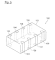
- the dielectric ceramic composition of the present invention may be applied to, for example, a common mode filter 100 shown in Figs. 5 and 6 , other than a multilayer complex electronic device.
- the common mode filter 100 comprises a filter portion constituted by a coiled conductor and a non-magnetic layer, and an external layer constituted by a magnetic layer
- the non-magnetic layer can be constituted by the dielectric ceramic composition of the present invention.
- the coiled conductor may be constituted by Ag having low DC resistance.
- a common mode filter according to the present embodiment may be produced by producing and stacking a non-magnetic green sheet and a magnetic green sheet.
- a common mode filter As shown in Fig. 5 , external electrodes 102 to 109 are formed on a main multilayer portion 101.
- This main multilayer portion 101 is constituted as shown in Fig. 6 . Namely, at first, it is formed that coiled conductors 111 to 114 are helically wound around non-magnetic layers 122 to 125 of a filter portion, coiled conductors 131 to 134 are helically wound around non-magnetic layers 142 to 145 of the filter portion.
- the non-magnetic layers 122 to 125 wherein the coiled conductors 111 to 114 are formed, and the non-magnetic layers 142 to 145 wherein the coiled conductors 131 to 134 are formed, are formed as they are sandwiched by non-magnetic layers 120, 121 and magnetic layers 146 to 148 via intermediate layers 140, 141.
- the coiled conductors 111 and 112 are connected via a through hole electrode 115 to form a coil 151. Also, coiled conductors 113 and 114 are connected via a through hole electrode 116 to form a coil 152. Then, these coils 151 and 152 are magnetically coupled.
- coils 161 and 162 are, as shown in Fig. 6 , formed by coiled conductors 131 to 134 and through hole electrodes 135, 136 to be magnetically coupled each other.
- the dielectric ceramic composition of the present invention may be applied to a non-magnetic layer of a multilayer ceramic coil having a coil portion constituted by stacking a coiled conductor and a non-magnetic layer.
- it is preferred to use Ag as a coiled conductor.
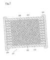
- it may be applied to a multilayer ceramic capacitor comprising an element body 210, wherein dielectric layers 202 and internal electrode layers 203 are alternately stacked, and both end portions of which external electrodes 204 are formed.
- Ag as a conductive material in the internal electrode layer.
- the dielectric ceramic composition of the present invention may be applied to a non-magnetic layer of a multilayer complex electronic device wherein a common mode filter shown in Fig. 6 and a multilayer ceramic capacitor shown in Fig. 7 are multilayered with complexation.
- MgO, ZnO, CuO, SiO 2 as a main component material constituting a dielectric ceramic composition material and B 2 O 3 -SiO 2 -BaO-CaO-based glass as a subcomponent material was prepared.
- B 2 O 3 -SiO 2 -BaO-CaO-based glass a commercial glass was used. And a glass softening point of the glass was 700°C.
- the B 2 O 3 -SiO 2 -BaO-CaO-based glass as a subcomponent material was added to the calcined powder, wet mixed by a ball mill for 16 hours, and the obtained slurry was dried by a dryer to obtain a material of a dielectric ceramic composition material according to the present invention.
- an acrylic resin di luted by a solvent was added as an organic binder, and after granulating, it was subject to pressure forming to obtain a discoid pressed article with a diameter of 12 mm and a thickness of 6 mm.
- the pressed article was fired in the air under a condition of 900°C-2h to obtain a sintered body.
- a density of the sintered body was calculated based on dimensions and weight of the sintered body after firing to calculate a relative density as the density of the sintered body with respect to theoretical density.
- the relative density of 90% or more was evaluated as GOOD. The results are shown in Table 1.
- a resistance value was measured after applying 25V of DC at 25°C for 30 seconds by using an insulation resistance meter (4329A by HEWLETT PACKARD). Based on the measurement, and an electrode area and a thickness of the sintered body, an insulation resistance p( ⁇ m) was calculated. In the present example, 20 samples were subject to measurement to obtain the average, which was used for evaluation. As an evaluation criterion, those of 1.0 ⁇ 10 10 ⁇ m or more were evaluated as GOOD. The results are shown in Table 1.
- sample 22 was confirmed to have crystal phase comprising crystal structure of Zn 2 SiO 4 and Mg 2 Si 2 O 6 .
- crystal phase comprising crystal structure of Mg 2 SiO 4 , Zn 2 SiO 4 and Mg 2 Si 2 O 6 were confirmed.
- Samples 24 to 28 were confirmed to have the same of Mg 2 SiO 4 and Zn 2 SiO 4 .
- samples 29 and 30 were confirmed to have ZnO residue in addition to crystal phase comprising crystal structure of Mg 2 SiO 4 and Zn 2 SiO 4 .
- coefficients of linear expansion can be changed arbitrarily within a range of 40 to 120x10 -7 /°C, while maintaining good properties of specific permittivity, insulation resistance and f ⁇ Q Value. This can also be explained by the following results of X-ray diffraction.
- FIG. 8 shows X-ray diffraction chart of samples 34, 37 and 40.
- FIG. 9 shows X-ray diffraction chart of Mg 2 SiO 4 (forsterite) and Zn 2 SiO 4 (willemite).
- sample 34 was confirmed that it only has crystal phase comprising crystal structure of Mg 2 SiO 4
- sample 37 has the same of Mg 2 SiO 4 and Zn 2 SiO 4
- sample 40 has the same of Zn 2 SiO 4 alone.
- samples 34, 37 and 40 were confirmed to have crystal phase comprising crystal structure of Mg 2 SiO 4 and/or Zn 2 SiO 4 , even the samples were sintered at a low temperature, i.e. 900°C, Note that, considering X-ray diffraction chart of sample 34, Zn was confirmed to be solid dissolved in Mg 2 SiO 4 in the sample 34.
- samples 31 to 33 were confirmed to have crystal phase comprising crystal structure of Mg 2 SiO 4 alone and samples 35, 36, 38 and 39 were confirmed to have the same of Mg 2 SiO 4 and Zn 2 SiO 4 .
- a dielectric ceramic composition according to the present invention when applied to a multilayer complex electronic device, it is possible to co-fire with a dielectric layer by matching with coefficients of linear expansion of dielectric layers which constitute capacitor portion, so that a multilayer complex electronic device having non-electronic layer with the above favorable properties can be provided. Additionally, since the dielectric ceramic composition according to the present invention shows sufficient sinterability even at 900°C, as conductive material, Ag can be used in a multilayer complex electronic device according to the present invention.
- a dielectric ceramic composition of the present invention is favorably used for a multilayer common mode filter, a multilayer ceramic coil, a multilayer ceramic capacitor wherein a conductive material is composed of Ag according to the present invention.
Landscapes
- Engineering & Computer Science (AREA)
- Chemical & Material Sciences (AREA)
- Power Engineering (AREA)
- Ceramic Engineering (AREA)
- Manufacturing & Machinery (AREA)
- Microelectronics & Electronic Packaging (AREA)
- Inorganic Chemistry (AREA)
- Materials Engineering (AREA)
- Structural Engineering (AREA)
- Organic Chemistry (AREA)
- Coils Or Transformers For Communication (AREA)
- Fixed Capacitors And Capacitor Manufacturing Machines (AREA)
- Compositions Of Oxide Ceramics (AREA)
- Inorganic Insulating Materials (AREA)
- Filters And Equalizers (AREA)
Abstract
Description
- The present invention relates to a dielectric ceramic composition available to be sintered at a low temperature having low specific permittivity, and a multilayer type electronic device such as a multilayer complex electronic device, a multilayer common mode filter, a multilayer ceramic coil and a multilayer ceramic capacitor and the like wherein a dielectric ceramic composition as a dielectric layer is applied.
- In recent years, with a demand for reduction in size, for high performance and high frequency on an electronic device such as a cell phone and the like used in a communication field, a demand for LC complex electronic device, a common mode filter and the like having high attenuation characteristic at high frequency region is rapidly increased.
- At present, Ni-Cu-Zn-based ferrite as a magnetic substance or Cu-Zn-based ferrite as a non-magnetic substance is used for a coil portion of LC complex electronic device or a common mode filter. However, effect of stray capacitance tends to be received by above material, because a specific permittivity of above material is about 15, which is comparatively high. Therefore, there is a limit for responding to the high frequency, thus, a material having further low specific permittivity is required. Also, for further high performance, a material having f · Q value and high dielectric resistance is required.
- Such the LC complex electronic device, a common mode filter, a multilayer type LC complex device having a common mode are formed by cofiring different materials (for example, a capacitor portion and a coil portion). Therefore, it is necessary that coefficients of linear expansion of different materials should be conformed as far as possible. Also, for reducing cost and a direct current resistance of a conducting material, it is preferable to use a conducting material including Ag, it is required that a material which can be sintered at lower temperature less than a softening point of Ag (for example, 950°C or lower) too.
- For example, Japanese Patent Gazette
No. 3030557 - However, in the Japanese Patent Gazette
No. 3030557 - Also, in
Japanese Patent Laid Open Nos. 2001-247359 2002-29826 2002-29827 - In
Japanese Patent Laid Open No. 2003-95746 - In
WO:2005/082806 , a dielectric ceramic material wherein a borosilicate glass is added to a forsterite and a calcium titanate is disclosed. However, in theWO2005/082806 , because coefficients of linear expansion of samples of embodiments are not disclosed, thus, it was unclear as to whether it is possible to respond for cofiring with materials having various coefficients of linear expansion. - The present invention has been made by considering actual circumstances, and purpose of the present invention is to provide a dielectric ceramic composition having relatively low contents of a glass component, which is available to be sintered at a low temperature (for example less than 950°C or less), and showing excellent characteristic (specific permittivity, f· Q-value, insulation resistance) as well as available to cofiring of different materials. Also, another purpose of the present invention is to provide a multilayer complex electronic device such as a multilayer common mode filter, a multilayer type filter, a multilayer ceramic coil and a multilayer ceramic capacitor having a non-magnetic layer constituted by the dielectric ceramic composition.
- In order to achieve the above purpose, a dielectric ceramic composition according to the present invention comprises; as a main component, Cu oxide, Si oxide and one selected from the group consisting of Zn oxide alone and a combination of Mg oxide and Zn oxide, as a subcomponent, a glass component including B oxide and at least one selected from the group consisting of Si oxide, Ba oxide, Ca oxide, Sr oxide, Li oxide and Zn oxide, and having a glass softening point is 750°C or less, wherein; a content of said glass component is 1.5 to 15wt% with respect to 100wt% of said main component.
- In the present invention, a glass component of which softening point is 750 °C or less having the above composition is included in the above mentioned range. This will allow to obtain a dielectric ceramic composition which is available to be sintered at a low temperature and to realize excellent characteristic (low specific permittivity, high f·Q-value, high insulation resistance).
- Preferably, crystal phase comprising crystal structure of forsterite and/or willemite is included in the dielectric composition. When oxides of the above main component have crystal phase comprising crystal structure of forsterite (Mg2SiO4) and/or willemite (Zn2SiO4), and further, Cu is dissolved in the crystal phase, the above mentioned effect can further be improved.
- Preferably, when said main component is shown by a general formula "a (bMgO·cZnO·dCuO)·SiO2", "a" is 1.5 to 2.4, "c:" is 0.10 to 0.98, "d" is 0.02 to 0.18 (note that, b+c+d=1.00).
- By setting a, b, c, d in the above mentioned general formula within the above range, the above mentioned effect can be improved further. Particularly, by changing a proportional ratio of "a", "b" and "c", crystal phase comprising crystal structure of forsterite and willemite can be produced, and its content ratio of Zn2SiO4 whose coefficient of linear expansion is 40×10-7/°C and Mg2SiO4 whose coefficient of linear expansion is 120×10-7/°C can be changed. Therefore, coefficient of linear expansion of the obtained dielectric ceramic composition can be changed arbitrarily, for example, within a range of 40 to 120×10-7/°C. As a result, it becomes possible to perform cofiring with materials having various coefficients of linear expansion.
- A multilayer complex electronic device according to the present invention comprises a coil portion constituted by a coiled conductor and a non-magnetic layer, and a capacitor portion constituted by an internal electrode layer and a dielectric layer, wherein said coiled conductor and/or said internal electrode layer include(s) Ag as a conductive material, said non-magnetic layer is constituted by any one of the above described dielectric ceramic compositions.
- A multilayer common mode filter according to the present invention comprises a filter portion constituted by a coiled conductor and a non-magnetic layer, and an external layer portion constituted by a magnetic layer, wherein said coiled conductor includes Ag as a conductive material, said non-magnetic layer is constituted by any one of the above described dielectric ceramic compositions.
- A multilayer complex electronic device according to the present invention comprises a capacitor portion constituted by an internal electrode layer and a dielectric layer, a common mode filter portion comprising a coiled conductor and a non-magnetic layer, and an external layer portion constituted by a magnetic layer, wherein said coiled conductor and/or said internal electrode layer include (s) Ag as a conductive material, said non-magnetic layer is constituted by any one of the above described dielectric ceramic compositions.
- A multilayer ceramic coil according to the present invention comprises a coil portion constituted by stacking a coiled conductor and a non-magnetic layer, wherein said coiled conductor includes Ag as a conductive material, said non-magnetic layer is constituted by any one of the above described dielectric ceramic compositions.
- A multilayer ceramic capacitor according to the present invention comprises an element body wherein an internal electrode layer and a dielectric layer are alternately stacked, wherein said internal electrode layer includes Ag as a conductive material, said dielectric layer is constituted by any one of the above described dielectric ceramic compositions.
- According to the present invention, by relatively decreasing a content of a glass component including the above mentioned oxides with respect to the above mentioned main component so as to be a specific range, without reduction in reliability, it is possible to obtain a highly reliable dielectric ceramic composition showing excellent properties (specific permittivity, loss Q value, insulation resistance, etc.). Also, since a glass softening point is 750°C or lower, it is possible to fire at a low temperature (for example, 900°C or lower).
- Further, by controlling a content ratio of Mg oxide and Zn oxide, content ratio of Zn2SiO4 whose coefficient of linear expansion is 40×10-7/°C and Mg2SiO4 whose coefficient of linear expansion is 120×10-7/°C can be changed. Therefore, coefficients of linear expansion of dielectric ceramic composition can be changed arbitrarily within, for example, 40 to 120×10-7/°C, while maintaining excellent properties. As a result, a desired coefficient of linear expansion can be obtained.
- By applying such a dielectric ceramic composition to a non-magnetic layer and a dielectric layer, it is possible to conform mostly to coefficients of linear expansion of materials facing these layers. Therefore, it becomes possible to perform cofiring with materials having various coefficients of linear expansion, while showing the above described excellent properties. Also, since it is possible to fire at a low temperature (for example, 950°C or lower), Ag which is low in DC resistance, is usable.
-
-
FIG. 1 is a perspective view of a LC complex electronic device according to an embodiment of the present invention; -
FIG. 2 is a cross sectional view of the LC complex electronic device along II-II line shown inFIG. 1 ,; -
FIG. 3 is an exploded perspective view showing a laminate structure of the LC complex electronic device according to an embodiment of the present invention; -
FIG. 4A is a circuit diagram of a L-shaped circuit,FIG. 4B is a circuit diagram of a n-shaped circuit, andFIG. 4C is a circuit diagram of a T-shaped circuit; -
FIG. 5 is a perspective view of a multilayer common mode filter according to another embodiment of the present invention; -
FIG. 6 is an exploded perspective view showing a laminate structure of a multilayer common mode filter according to another embodiment of the present invention; and -
FIG. 7 is a cross sectional view of a multilayer ceramic capacitor according to another embodiment of the present invention. -
FIG. 8 is X-ray diffraction chart of examples of the present invention. -
FIG. 9 is X-ray diffraction chart of Mg2SiO4 and Zn2SiO4 - Hereinafter, the present invention will be described based on embodiments shown in drawings.
- As shown in
FIG. 1 , a LC complex electronic device as a multilayer complexelectronic device 1 according to an embodiment of the present invention comprises amultilayer portion 11 as a main portion,external electrodes external electrodes external electrode 20 in the front side face in the figure, anexternal electrode 29 in the back side face in the figure. The shape of the LC complexelectronic device 1 is, although not particularly limited, normally a rectangular parallelepiped. Also, the size, which is not particularly limited and determined appropriately depending on the application, is normally (0.8 to 3.2 mm) × (0.6 to 1.6 mm) × (0.3 to 1.0 mm) or so. First, a structure of a LC complex electronic device according to the present embodiment will be described. -
FIG. 2 is a sectional view of the LC complexelectronic device 1 along II-II line shown inFIG. 1 . The LC complexelectronic device 1 according to the present embodiment comprises a capacitor portion 30 (C) in the lower layer portion and a coil portion 40(L) in the upper layer portion. Thecapacitor portion 30 is a multilayer capacitor wherein a plurality ofdielectric layers 32 is formed betweeninternal electrodes 31. On the other hand, in thecoil portion 40, acoiled conductor 41 having a predetermined pattern is formed in anon-magnetic layer 42.
Thedielectric layer 32 constituting thecapacitor portion 30 and/or thenon-magnetic layer 42 constituting thecoil portion 40 include a dielectric ceramic composition according to the present invention. However, preferably, thenon-magnetic layer 42 is constituted by a dielectric ceramic composition of the present invention, thedielectric layer 32 to constitute thecapacitor portion 30 is constituted by a dielectric ceramic composition of titanium oxide based having relatively high specific permittivity. - The dielectric ceramic composition of the present invention includes, as a main component, Cu oxide, Si oxide and one selected from Zn oxide alone and a combination of Mg oxide and Zn oxide.
- The above described oxides included as the main component may be shown as "a(bMgO·CZnO·dCuO)·SiO2" by using a general formula. The "a" in the general formula shows a mole ratio of A/B of Mg, Zn and Cu shown as A site atom and Si shown as B site atom. In the present embodiment, the "a" is preferably 1. 5 to 2.4, more preferably 1.6 to 2.0. When the "a" is too smali, sintering at lower temperature becomes insufficient and an insulating resistance and a f·Q value tend to deteriorate.
- The "b", "c" and "d" in the above described general formula respectively show a content ratio of MgO, ZnO and CuO (a mole ratio) to whole oxide of A site atom. Thus, b+c+d=1.00.
- In the present embodiment, the "c" is preferably 0.10 to 0.92, more preferably 0. 15 to 0. 92. Also, the "d" is preferably 0.02 to 0.18, more preferably 0.04 to 0.14.
Note that, the "b" is within a range of "1.00-c-d". Thus, when the "b" is 0, namely, there will be a possibility a case that MgO is not included, however, the "b" is preferably larger than 0 by a reason mentioned below. - It may be considered that the dielectric ceramic composition of the present embodiment has a composite structure wherein Mg2SiO4 having crystal structure of forsterite and Zn2SiO4 having crystal structure of willemite are coexisted.
- Generally, Mg2SiO4 and Zn2SiO4 both have high melting point., and that they do not sinter at a low temperature, e.g. 950°C or less.
- However, in the present embodiment, Cu, included as a main component, is dissolved in either or both of Mg2SiO4 (forsterite) and Zn2SiO4 (willemite). Further, according to contents of Mg and Zn, Mg may be dissolved in Zn2SiO4 or Zn may be dissolved in Mg2SiO4.
- When the other atom is dissolved in Mg2SiO4 and Zn2SiO4, their producing temperatures become low, therefore, even when a content of glass component is decreased, it is likely to sinter at a low temperature, e.g. 950°C or less.
- Further, the dielectric ceramic composition of the present embodiment produces crystal phase comprising crystal structure of forsterite and/or willemite by controlling a, b and c in the above general formula. Therefore, coefficient of linear expansion of the dielectric ceramic composition of the embodiment is proportional to content ratio of Mg2SiO4 and Zn2SiO4. Namely, coefficients of linear expansion is determined by a content ratio of b (MgO) and c(ZnO) . Note that the dielectric ceramic composition of the embodiment may include any crystal phase except for a crystal phase comprising crystal structure of forsterite and willemite, however, the same of enstatite (Mg2Si2O6) and the like are not preferable.
- Therefore, by controlling a content ratio of b(MgO) and c(ZnO), coefficient of linear expansion of a (bMgO·cZnO·dCuO)·SiO2 can be changed arbitrarily.
- Here, a coefficient of linear expansion of Zn2SiO4 alone is smaller than the same of Mg2SiO4 alone, and is about 1/3 of the same of Mg2SiO4 alone. Specifically, since a coefficient of linear expansion of Mg2SiO4 is an about 120×10-7/°C, a coefficient of linear expansion of 2n2SiO4 is an about 40×10-7/°C, a coefficient of linear expansion of the dielectric ceramic composition of the present embodiment may be changed arbitrarily within a range of about 40 to 120×10-7/°C.
- In the present embodiment, when the "c" is too small, sintering at lower temper-ature becomes insufficient and an insulating resistance and a f·Q value tend to deteriorate.
- Also, in the present embodiment, when the "d" is too small, sintering at lower temperature becomes insufficient and an insulating resistance and a f·Q value tend to deteriorate. To the contrary, when the "d" is too large, the insulating resistance and the f·Q value tend to deteriorate.
- Also, the dielectric ceramic composition of the present embodiment comprises, other than the above described main component, a glass component, as a subcomponent, including B oxide and at least one selected from Si oxide, Zn oxide, Ba oxide, Ca oxide, Sr oxide and Li oxide. This glass component is a low-melting glass having a glass softening point of 750°C or lower. Note that the glass softening point is measured by JIS-R-3103.
- Since the dielectric ceramic composition of the present embodiment has a glass component having a glass softening point is 750°C or lower, it becomes possible to perform a low temperature sintering, for example, at 950°C or lower, and it is available to apply to an electronic device wherein an internal electrode is constituted by Ag having a low DC resistance.
- This glass component is not particularly limited as far as this including B oxide and at least one selected from Si oxide, Zn oxide, Ba oxide, Ca oxide, Sr oxide and Li oxide and having a glass softening point of 750°C or lower. As these glass components, for example, B2O3-SiO2-BaO-CaO-based glass, B2O3-SiO2-BaO-based glass, B2O3-SiO2-CaO-based glass, B2O3-SiO2-SrO-based glass, B2O3-SiO2Li2O-based glass, B2O3-ZnO-BaO-based glass, B2O3-ZnO-Li2O-based glass, B2O3-SiO2-ZnO-BaO-based glass, B2O3-SiO2-ZnO-BaO-CaO-based glass, etc., may be mentioned. And, B2O3-SiO2-BaO-CaO-based glass and B2O3-SiO2-SrO-based glass are preferable as the glass component.
- A content of the glass component is 1.5 to 15wt%, preferably 3 to 5wt% with respect to 100wt% of the main component.
- When the content of the glass component is too low, there is a tendency not to obtain sufficient sinterability at a low temperature (for example, 950°C or lower). In contrast, when it is too large, a f·Q value tends to deteriorate, and reduction in reliability as an electronic device.
- In case that the
dielectric layer 32 does not include a dielectric ceramic composition of the present invention, as a dielectric material to constitute thedielectric layer 32, it is preferable to use a dielectric ceramic composition based titanium oxide, which is available to fire at 950°C or lower. As the dielectric ceramic composition based titanium oxide, a material including titanium oxide, barium titanate, calcium titanate, strontium titanate, zinc titanate, nickel titanate and the like as a main component, and as a subcomponent, material including more than one kind, such as Cu oxide, Mn oxide and glass which include B oxide and whose glass softening point is 750°C or lower are exemplified. - An average crystal grain size of a sintered dielectric crystal grain constituting the
dielectric layer 32 is preferably 1.5µm or less, more preferably 1.0µm or less. The lower limit of the average crystal grain size is not particularly limited, normally 0.5µm or so. When the average crystal grain size of the dielectric crystal grain is too large, insulation resistance tends to deteriorate. - The average crystal grain size of the dielectric crystal grain can be obtained by, for example, cutting the
dielectric layer 32 to observe the cutting surface with SEM, measuring crystal grain sizes of the predetermined number of dielectric crystal grains, and calculating based on the measurement results. Note that a crystal grain size of each dielectric crystal grain can be obtained by, for example, a coding method wherein each crystal grain is assumed as a sphere. Also, at calculation of the average crystal grain size, the number of grains subject to measurement of the crystal grain size is normally 100 or more. - A thickness (g) of the
dielectric layer 32 in a portion sandwiched by a pair ofinternal electrodes 31 is preferably 30µm or less, more preferably 20µm or less. - A thickness of the
internal electrode 31 is not particularly limited, and it may be suitably determined in response to the thickness of thedielectric layer 32. - In the present embodiment, a
non-magnetic layer 42 includes a dielectric ceramic composition of the present invention. When it does not include, as a non-magnetic material to constitute the non-magnetic layer is, for example, non-magnetic Cu-Zn based ferrite, a glass materials are exemplified. - A conducting material included in the
internal electrode 31 constituting thecapacitor portion 30 or in the coiledconductor 41 constituting thecoil portion 40 are not particularly limited, since the dielectric ceramic composition of the present invention can be fired at a low temperature (for example, 950°Cor lower), Ag with low DC resistance may be used as a conducting material in the present embodiment. Also, by blending a dielectric material constituting thedielectric layer 32 and a non-magnetic material constituting the non-magnetic: layer 92, the blended material may be used as an intermediate portion between thecapacitor portion 30 and thecoil portion 40. A thickness of the intermediate portion is 10 to 100µm. By providing the intermediate portion, an interface bonding characteristic between the capacitor portion and the coil portion can be improved. - As
external electrodes 20 to 29, although they are not particularly limited, an electric conductor including Ag can be used, and are preferably plated with Cu-Ni-Sn, Ni-Sn, Ni-Au, Ni-Ag, etc. - The LC complex electronic device of the present embodiment is produced by, as with conventional LC complex electronic device, preparing a non-magnetic green sheet and a dielectric green sheet, stacking these green sheets, forming a green-
state multilayer portion 11, and formingexternal electrodes 20 to 29 after firing. Hereinafter, the production method will be specifically described. - First, a material of a non-magnetic material to constitute the
non-magnetic layer 42 is prepared. In the present embodiment, as a material of the non-magnetic material, a material of the dielectric ceramic composition is used. - As a main component material of the dielectric ceramic composition of the present invention, Mg oxide, Zn oxide, Cu oxide and Si oxide as well as mixture thereof and composite oxide can be used. It is also possible to properly select from a variety of compounds to become the above oxide or composite oxide by firing, for example, carbonate, oxalate, nitrate, hydroxide, organic metallic compound, etc. , and to mix for use.
- Also, as a material of the glass component which is a subcomponent of the dielectric ceramic compound of the present invention, an oxide constituting the above mentioned glass component, mixture thereof and composite oxide, in addition to a variety of compounds to become the oxide or composite oxide constituting the glass component by firing, can be used.
The glass component can be obtained by mixing materials including oxide, etc., which constitutes the glass component, firing followed by rapid cooling, and vitrifying. - In the present embodiment, the respective main component materials are blended. Also, in response to necessity, a subcomponent other than glass component may be added to the main component materials to mix. As a method of mixing each of the main component material and subcomponent material, although not particularly limited, for example, there may be mentioned a method of dry-mixing material powders in a powdery state, or of wet-mixing material powders, to which water, organic solvent, etc. is added, by using a ball mill, etc.
- Next, the above obtained mixture of powder is subject to calcine. The calcine is performed at a holding temperature of preferably 850 to 1100°C, for a temperature holding time of preferably 1 to 15 hours. The calcine may be performed in the air, in an atmosphere having higher oxygen partial pressure than that in the air, or pure oxygen atmosphere.
- Next, the powder obtained by calcine is pulverized to prepare a pre-fired powder and blended by adding a glass component material as the subcomponent. As a method of preparation, although not particularly limited, for example, there may be mentioned a method to add water, organic solvent, etc., to the calcined powder obtained by calcining and then to wet-mix them by using a ball mill, etc. Then, the obtained pre-fired powder is made a paste, so that a non-magnetic layer paste is prepared.
- The non-magnetic layer paste may be either an organic paste wherein the pre-fired powder and organic vehicle are kneaded or water-based paste.
- A coil conductor paste is obtained by kneading a conducting material, for example Ag and the like and the above organic vehicle.
- A content of the organic vehicle in each of the above paste is not particularly limited and may be a normal content, for example, about 5 to 15wt% of a binder and about 50 to 150wt% of a solvent with respect to 100wt of the powder before firing. Also, each paste may include an additive selected from a variety of dispersants, plasticizers, etc., if needed. The total content is preferably 10wt% or less.
- Next, the non-magnetic layer paste is made a sheet by a doctor blade method, etc., to form a non-magnetic green sheet.
- Next, a coil conductor is formed on the above produced non-magnetic green sheet. Forming the coil conductor is that a coil conductor paste is formed on the non-magnetic green sheet by a screen printing method and the like. Note that, although a forming pattern of the coil conductor may suitably selected in response to a circuit constitution and the like of a produced LC complex electronic device, in the present embodiment, they will be each patterns mentioned below.
- Next, on the non-magnetic green sheet, through holes are formed. Although a producing method of the through hole is not particularly limited, for example, it can be performed by a laser processing and the like. Note that, a forming position of the through hole is not particularly limited, if it is on a coil conductor, it is preferable to form at an end portion of the coil conductor, in the present embodiment, they will be each position mentioned below.
- First, a main component material of a dielectric material to constitute the
dielectric layer 32 is prepared to make a paste so that the dielectric layer paste is obtained. The dielectric layer paste may be prepared as similar with the above mentioned non-magnetic layer paste. - As a main component material, titanium oxide, barium titanate, calcium titanate, strontium titanate, zinc titanate, nickel titanate and the like may be used. It is also possible to properly select from variety of compounds to become the above oxide or composite oxide by firing, for example, carbonate, oxalate, nitrate, hydroxide, organic metallic compound, etc., and to mix for use. In addition, as a material of the dielectric material, starting material of subcomponents may be included in response to the necessity other than the above main component.
- Note that before making the dielectric layer paste from the dielectric material, each starting material constituting the dielectric material may be preliminarily sintered, and may be pulverized the powder thereafter.
- An internal electrode paste is prepared by kneading Ag as a conducting material and the above described organic vehicle.
- Then, the dielectric layer paste is made a sheet by a doctor blade method, etc., to form a dielectric green sheet. Also, internal electrodes are formed on the dielectric green sheet in response to the necessity. The internal electrodes may be formed by printing an internal electrode paste by screen printing method and the like.
- Next, each of the above obtained dielectric green sheet and non-magnetic green sheet are alternately stacked sequentially to form a green-
state multilayer portion 11. - In the present embodiment, the green-
state multilayer portion 11 is, as shown inFIG. 3 , produced by stacking a plurality of dielectric green sheets wherein the internal electrode constituting the capacitor portion is formed, and on it, stacking a plurality of the non-magnetic green sheets wherein the coiled conductor constituting the coil portion is formed. - Below, a stacking process of the green sheets will be described in detail.
- First, in the lowest layer, a dielectric
green sheet 32f wherein the internal electrode is not formed is placed, a dielectricgreen sheet 32a wherein theinternal electrode 31a having a pair ofderivation portions derivation portions - Next, on the dielectric
green sheet 32a wherein theinternal electrode 31a is formed, a dielectricgreen sheet 32b wherein theinternal electrode 31b having aderivation portion 25a is formed is stacked. Thederivation portion 25a is projected in an end portion of the dielectric green sheet from a back side of lateral direction X of the dielectric green sheet. - Next, on the dielectric
green sheet 32a wherein theinternal electrode 31a is formed, the dielectricgreen sheet 32c wherein theinternal electrode 31c having aderivation portion 26a is formed is stacked. Thederivation portion 26a is projected in an end portion of the dielectric green sheet from a lateral portion of a back side of lateral direction X of the dielectric green sheet. Note that, thederivation portion 26a is arranged at a back side along a longitudinal direction Y of the dielectric green sheet with respect to thederivation portion 25a. - Next, by stacking the dielectric
green sheet 32a wherein theinternal electrode 31a is formed, thereon, the dielectricgreen sheet 32d wherein theinternal electrode 31d having aderivation portion 27a is formed is stacked. Thederivation portion 27a is arranged at a back side along a longitudinal direction Y of the dielectric green sheet with respect to thedeviation portion 26a, - Next, by stacking the dielectric
green sheet 32a wherein theinternal electrode 31a is formed, thereon, the dielectricgreen sheet 32e wherein theinternal electrode 31e having aderivation portion 28a is formed is stacked. Thederivation portion 28a is arranged at a back side along a longitudinal direction Y of the dielectric green sheet with respect to thedeviation portion 27a. - Finally, by stacking the dielectric
green sheet 32a wherein theinternal electrode 31a is formed, green-state single-layer capacitors 30a to 30e are thus formed wherein the respective derivation portions are formed at different positions along a longitudinal direction Y of the dielectric green sheet. - Next, on the above-obtained green-state capacitor portion, coil portions are formed.
- First, on the capacitor portions, a non-magnetic green sheet 42g wherein the coiled conductor is not formed is stacked, thereon, a non-magnetic
green sheet 42a wherein fourcoil conductors 41a respectively havingderivation portions - Next, a non-magnetic
green sheet 42b wherein four approximately U-shapedcoiled conductors 41b are formed is stacked thereon. Note that, as shown inFig.3 , the approximately U-shapedcoiled conductors 41b are arranged so as to have these curved portions in a front side of lateral direction X of the non-magnetic green sheet. Note that, a throughhole 51b is formed in one end of the coiledconductor 41b, and thecoiled conductor 41a and thecoiled conductor 41b are connected via this throughhole 51b by using a conductive paste. - Next, a non-magnetic
green sheet 42c wherein four approximately C-shapedcoiled conductors 41c are formed is stacked thereon. Note that the approximately C-shapedcoiled conductor 41c is arranged so as to have its curved portion in a front side of longitudinal direction Y of the non-magnetic green sheet. Note that, as shown inFig.3 , a throughhole 51c is formed in one end of the coiledconductor 41c, and thecoiled conductor 41b and the coiledconductor 41c are connected via this throughhole 51c by using a conductive paste. - Next, a non-magnetic
green sheet 42d wherein four approximately C-shapedcoiled conductors 41d are formed is stacked thereon. Note that the approximately C-shapedcoiled conductor 41d is arranged so as to have its curved portion in a front side of longitudinal direction Y of the non-magnetic green sheet. Note that, as shown inFig.3 , a throughhole 51d is formed in one end of the coiledconductor 41d, and the coiledconductor 41c and thecoiled conductor 41d are connected via this throughhole 51d by using a conductive paste. - Next, a non-magnetic
green sheet 42e wherein four approximately U-shapedcoiled conductors 41e are formed is stacked thereon. Note that, the approximately U-shapedcoiled conductors 41e are arranged so as to have these curved portions in a back side of lateral direction X of the non-magnet.ic green sheet. Note that, as shown inFig.3 , a throughhole 51e is formed in one end of the coiledconductor 41e, and thecoiled conductor 41d and thecoiled conductor 41e are connected via this throughhole 51e by using a conductive paste. - Next, a non-magnetic green sheet 42f wherein, four
coiled conductors 41f are formed is stacked thereon. The fourcoiled conductors 41f respectively have derivation portions 21b, 22b, 2.3b, 2.4b whose one ends project from a front side of lateral direction of the non-magnetic green sheet. Note that, a throughhole 51f is formed in one end of the coiledconductor 41f, and thecoiled conductor 41e and thecoiled conductor 41f are connected via this throughhole 51f by using a conductive paste. - Finally, a non-magnetic
green sheet 42h wherein a coiled conductor is not formed is stacked on the non-magnetic green sheet 42f wherein thecoiled conductor 41f is formed. - As described above, by jointing the coiled conductor on each non-magnetic green sheet via each through hole, a coil is formed.
- Next, the green-state multilayer portion obtained by alternately stacking the dielectric green sheet and the non-magnetic green sheet is fired. Firing conditions include a temperature rising rate of preferably 50 to 500°C/hour and further preferably 200 to 300°C/hour, a holding temperature of preferably 840 to 900°C, a temperature holding time of preferably 0.5 to 8 hours and further preferably 1 to 3 hours, and a cooling rate of preferably 50 to 500°C%hour and further preferably 200 to 300°C/hour.
- Next, the fired multilayer portion is subject to end surface polishing by, for example, barrel-polishing or sand blasting, etc. The external electrodes are formed by baking after applying an external electrode paste to both side surfaces of the multilayer portion followed by drying. The external electrode paste can be prepared by kneading a conducting material such as Ag and the above organic vehicle. Note that on thus-formed
external electrodes 20 to 29, it is preferable to electroplate with Cu-Ni-Sn, Ni-Sn, Ni-Au, Ni-Ag, etc. - When forming the external electrode, the
external electrodes 21 to 24 become input-output terminals by connecting to therespective derivation portions 21a to 24a of the coil portion. Theexternal electrode 25 to 28 become input-out.put terminals to connect the capacitor portion and the coil portion by connecting to eachderivation portions 25a to 28a of the capacitor portion andderivation portions 25b to 28b of the coil portion. Theexternal electrodes derivation portion - As described above, by forming each of the external 1
electrodes 20 to 29 in themultilayer portion 11, the LC complex electronic device of the present embodiment is resulted in configuring four L-shaped circuit shown inFIG. 4A . - Thus produced LC complex electronic device of the present embodiment is mounted on a printed-circuit board, etc., by soldering, etc. to use in a variety of electronic hardware, etc.
- Hereinbefore, embodiments of the present invention are described, but the present invention is not limited to the above-mentioned embodiments and can be variously modified within the scope of the present invention.
- For example, the above mentioned embodiment exemplifies the LC complex electronic device wherein the four L-shaped circuits are formed, but it can be a LC complex electronic device wherein another lumped-constant circuit is formed. As an example of another lumped-constant circuit, there may be mentioned n-shaped circuit shown in
FIG. 4B , T-shaped circuit shown inFIG. 4C , and double-n-shaped circuit formed by two n-shaped circuits. - In the above mentioned embodiment exemplifies a LC complex electronic device as a multilayer complex electronic device according to the present invention, but a multilayer complex electronic device according to the present invention is not limited to a multilayer type filter. Also, the dielectric ceramic composition of the present invention may be applied to, for example, a
common mode filter 100 shown inFigs. 5 and6 , other than a multilayer complex electronic device. Namely, in thecommon mode filter 100 comprises a filter portion constituted by a coiled conductor and a non-magnetic layer, and an external layer constituted by a magnetic layer, the non-magnetic layer can be constituted by the dielectric ceramic composition of the present invention. By making this, the coiled conductor may be constituted by Ag having low DC resistance. - A common mode filter according to the present embodiment, as similar with the above mentioned embodiment, may be produced by producing and stacking a non-magnetic green sheet and a magnetic green sheet.
- In a common mode filter, as shown in
Fig. 5 ,external electrodes 102 to 109 are formed on amain multilayer portion 101. Thismain multilayer portion 101 is constituted as shown inFig. 6 . Namely, at first, it is formed thatcoiled conductors 111 to 114 are helically wound aroundnon-magnetic layers 122 to 125 of a filter portion,coiled conductors 131 to 134 are helically wound aroundnon-magnetic layers 142 to 145 of the filter portion. Then, thenon-magnetic layers 122 to 125 wherein the coiledconductors 111 to 114 are formed, and thenon-magnetic layers 142 to 145 wherein the coiledconductors 131 to 134 are formed, are formed as they are sandwiched bynon-magnetic layers magnetic layers 146 to 148 viaintermediate layers - The
coiled conductors hole electrode 115 to form acoil 151. Also,coiled conductors hole electrode 116 to form acoil 152. Then, thesecoils - Similarly, coils 161 and 162 are, as shown in
Fig. 6 , formed bycoiled conductors 131 to 134 and throughhole electrodes - Then, the above described coiled
deviations 111a to 119a and 131a to 134a are respectively connected withexternal electrodes 102 to 109, and being to form input-output terminals - Also, the dielectric ceramic composition of the present invention may be applied to a non-magnetic layer of a multilayer ceramic coil having a coil portion constituted by stacking a coiled conductor and a non-magnetic layer. In this case, it is preferred to use Ag as a coiled conductor. Further, as shown in
Fig. 7 , it may be applied to a multilayer ceramic capacitor comprising anelement body 210, whereindielectric layers 202 and internal electrode layers 203 are alternately stacked, and both end portions of whichexternal electrodes 204 are formed. In this case, it is preferred to use Ag as a conductive material in the internal electrode layer. - Further, the dielectric ceramic composition of the present invention may be applied to a non-magnetic layer of a multilayer complex electronic device wherein a common mode filter shown in
Fig. 6 and a multilayer ceramic capacitor shown inFig. 7 are multilayered with complexation. In this case, it is preferred to use Ag as a conductive material incoiled conductors 111 to 114, 131 to 134 or theinternal electrode layer 203. - Hereinafter, the present invention will be described based on the further detailed examples, but the present invention is not limited to the examples.
- First, MgO, ZnO, CuO, SiO2 as a main component material constituting a dielectric ceramic composition material and B2O3-SiO2-BaO-CaO-based glass as a subcomponent material was prepared. Note that, as the B2O3-SiO2-BaO-CaO-based glass, a commercial glass was used. And a glass softening point of the glass was 700°C.
- Then, materials of the main components were weighed and compounded so that "a", "b", "c", "d" in a general formula a (bMgO·cZnO·dCuO)·SiO2 become values shown in Table 1 after sintering, and wet mixed by a ball mill for 24 hours. After wet mixing, the obtained slurry was dried by a dryer, followed by calcine at 1000°C of the dried mixture of powders in a batch furnace to obtain a calcined powder. The B2O3-SiO2-BaO-CaO-based glass as a subcomponent material was added to the calcined powder, wet mixed by a ball mill for 16 hours, and the obtained slurry was dried by a dryer to obtain a material of a dielectric ceramic composition material according to the present invention.
- Next, to the dielectric ceramic composition material, an acrylic resin di luted by a solvent was added as an organic binder, and after granulating, it was subject to pressure forming to obtain a discoid pressed article with a diameter of 12 mm and a thickness of 6 mm. The pressed article was fired in the air under a condition of 900°C-2h to obtain a sintered body.
- As for the obtained sintered body, a density of the sintered body was calculated based on dimensions and weight of the sintered body after firing to calculate a relative density as the density of the sintered body with respect to theoretical density. The relative density of 90% or more was evaluated as GOOD. The results are shown in Table 1.
- To the obtained sintered body, a specific permittivity (no unit) was calculated by a resonance method (JIS R 1627) with using a network analyzer (8510C by HEWLETT PACKARD). As an evaluation criterion, those of 7.50 or less were evaluated as GOOD. The results are shown in Table 1.
- Q value was measured under the same measurement conditions as the specific permittivity with multiplying a oscillation frequency fr thereto to evaluate f·Q Value (GHz). The higher f·Q value is preferable. As an evaluation criterion, those of 10000GHz or more were evaluated as GOOD. The results are shown in Table 1.
- First, as for the sintered body wherein electrodes were formed, a resistance value was measured after applying 25V of DC at 25°C for 30 seconds by using an insulation resistance meter (4329A by HEWLETT PACKARD). Based on the measurement, and an electrode area and a thickness of the sintered body, an insulation resistance p(Ω·m) was calculated. In the present example, 20 samples were subject to measurement to obtain the average, which was used for evaluation. As an evaluation criterion, those of 1.0×10¹⁰Ω·m or more were evaluated as GOOD. The results are shown in Table 1.
- To the obtained sintered body, a thermal expansion from a room temperature to 700°C was measured and a coefficient thermal expansion coefficient α (10-7/°C) was calculated by using a thermal expansion meter (TD5000SA by BRUKER AXS). The results are shown in Table 1.
- X-ray diffraction was performed to the obtained sintered body using an X-ray diffraction device (PANalytical-MPD by Spectris Co., Ltd.). Cu-Kα X-ray was used for an X-ray source. Measurement conditions were; voltage of 45 kV, electric current of 40 mA, and within a range of 2θ=20° to 60°, angular step width was set at 0.033° and counting time was 0.20 sec.
-
[Table 1] Sample No. subcomponent main component sintered body property glass mole ratio MgO ZnO CuO relative dencity specific permittiveity εs insulaton resistance ρ f·Q coefficient of linear expansion α (wt%) a b c d (Ω·m) (GHz) (x 10-7/°C) *1 1.0 2.0 0.66 0.26 0.08 75.7% 5.28 1.4E+08 5671 98.4 *2 1.0 2.0 0.56 0.26 0.18 88.2% 6.38 1.7E+10 8278 98.6 3 1.5 2.0 0.56 0.26 0.18 95.0% 7.35 9.7E+12 12057 98.0 4 3.0 2.0 0.66 0.26 0.08 92.5% 6.91 3.0E+12 31495 99.6 5 5.0 2.0 0.66 0.26 0.08 95.7% 7.30 5.9E+12 23259 100.8 6 7.0 2.0 0.66 0.26 0.08 95.6% 7.27 5.7E+12 17925 101.5 7 10.0 2.0 0.66 0.26 0.08 96.1% 7.30 2.6E+12 14357 103.6 8 15.0 2.0 0.66 0.26 0.08 95.4% 7.35 1.4E+12 11489 106.0 *9 16.0 2.0 0.66 0.26 0.08 95.0% 7.34 1.7E+12 7527 107.2 *10 20.0 2.0 0.66 0.26 0.08 94.7% 7.37 1.5E+12 4779 108.9 "*" shows comparative example
in Table, (mE+n) means (m × 10+n) - From Table 1, when a content of a glass component is less than a range of the present invention (
Samples 1, 2) , sintering at 900°C becomes insufficient. As a result of this, it can be confirmed that desired properties of insulation resistance and f·Q Value cannot be obtained. Also, when a content of the glass component is larger than a range of the present invention (Samples 9, 10), it can be confirmed that f·Q Value becomes deteriorated, even though the sinterability is sufficient.
Contrary to this, when a content of glass component is in a range of the present invention (Samples 3 to 8), it can be confirmed that sufficient sinterability and good property are shown. - Note that, according to the above X-ray diffraction, all the samples (
Samples 1 to 10) were confirmed to have crystal phase comprising crystal structure of Mg2SiO4 and Zn2SiO4. Further, crystal phase of glass composition was not confirmed and that it was considered forming noncrystalline grain boundary phase. - Except for changing the contents and the composition of the glass component to those shown in Table 2 and changing the "a", "b", "c" and "d" of the above described general formula to those shown in Table 2, a dielectric ceramic composition was produced as with
Sample 1, and same evaluation was performed as in Example 1. The results are shown in Table 2. Note that, a glass softening point of the respective glass components are temperatures shown in Table 2. -
[Table 2] Sample No subcomponent main component sintered body property glass mole ratio MgO ZnO CuO relative dencity specific permittiveit y ε s insulaton resistance ρ f·Q coefficient of linear expansion α component (wt%) softening point a b c d (Ω·m) (GHz) (×10-7/°C) 11 B2O3-SiO2-BaO 4.0 680 2.0 0.66 0.26 0.08 96.4% 6.97 1.5E+13 21400 98.4 12 B2O3-SiO2-CaO 4.0 720 2.0 0.66 0.26 0.08 96.0% 6.92 1.2E+13 17945 98.6 13 B2O3-SiO2-SrO 4.0 700 2.0 0.56 0.26 0.18 97.8% 7.15 1.5E+13 18438 98.0 14 B2O3-SiO2-Li2O 4.0 610 2.0 0.66 0.26 0.08 98.9% 7.34 1.0E+13 30249 99.6 15 B2O3-SiO2-BaO-CaO 4.0 700 2.0 0.66 0.26 0.08 95.0% 7.17 5.9E+12 26126 101.9 16 B2O3-ZnO-BaO 4.0 610 2.0 0.66 0.26 0.08 92.8% 6.59 1.2E+12 19000 101.5 17 B2O3-ZnO-Li2O 4.0 550 2.0 0.66 0.26 0.08 98.2% 7.30 5.9E+12 30119 103.6 18 B2O3-SiO2-ZnO-BaO 4.0 600 2.0 0.66 0.26 0.08 92.6% 6.58 9.3E+11 18727 106.0 19 B2O3-SiO2-ZnO-BaO-CaO 4.0 590 2.0 0.66 0.26 0.08 91.9% 6.59 4.8E+11 18298 107.2 *20 B2O3-SiO2-Al2O3 4.0 800 2.0 0.66 0.26 0.08 60.2% 5.03 4.7E+07 1822 108.9 *21 SiO2-ZnO-BaO 4.0 780 2.0 0.66 0.26 0.08 83.8% 5.74 5.5E+09 6249 109.9 "*" shows comparative example
in Table, (mE+n) means (m x 10+n) - From Table 2, when a composition of a glass component is not a composition of the present invention or a glass softening point is not within a range of the present invention (
Samples 20, 21), sintering at 900°C becomes insufficient, as a result, it can be confirmed that desired properties of insulation resistance and f·Q Value cannot be obtained.
Contrary to this, when a composition of glass component is a composition of the present invention and a glass softening point is within a range of the present invention (Samples 11 to 19), it can be confirmed that sufficient sinterability and good property are shown. - Note that, according to the above X-ray diffraction, all the samples (
Samples 11 to 21) were confirmed to have crystal phase comprising crystal structure of Mg2SiO4 and Zn2SiO4. - Except for changing the "a", "c", "d" in the above described generic formula to those shown in Tables 3 to 5, a dielectric ceramic composition was produced as with Example 1, and same evaluation was performed as in Example 1. The results are shown in Tables 3 to 5.
-
[Table 3] Sample No. subcomponent main component sintered body property glass mole ratio MgO ZnO CuO relative dencity specific permittiveity ε s insulaton resistance ρ f·Q coefficient of linear expansion α (wt%) a b c d (Ω·m) (GHz) (×10-7/°C) 22 4.0 1.0 0.66 0.26 0.08 53.9% 3.91 3.0E+07 1754 134.4 23 4.0 1.3 0.66 0.26 0.08 69.8% 4.90 2.6E+07 3862 116.9 24 4.0 1.6 0.66 0.26 0.08 90.1% 6.92 2.0E+12 23259 104.3 25 4.0 1.9 0.66 0.26 0.08 94.1% 7.08 5.9E+12 26104 103.5 26 4.0 2.0 0.66 0.26 0.08 95.0% 7.17 5.9E+12 26126 101.9 27 4.0 2.2 0.66 0.26 0.08 96.1% 7.27 3.3E+12 17520 99.2 28 4.0 2.4 0.66 0.26 0.08 96.3% 7.28 1.2E+12 10498 103.2 29 4.0 2.5 0.66 0.26 0.08 96.3% 7.29 1.0E+12 8503 104.5 30 4.0 2.7 0.66 0.26 0.08 95.0% 7.20 3.5E+10 2485 104.1 in Table, (mE+n) means (m × 10 +n) -
[Table 4] Sample No subcomponent main component sintered body property glass mole ratio MgO ZnO CuO relative dencity specific permittiveity ε s insulaton resistance ρ f·Q coefficient of linear expansion α (wt%) a b c d (Ω·m) (GHz) (×10-7/°C) *31 4.0 2.0 0.92 0.00 0.08 56.3% 4.61 5.4E+08 2401 123.1 32 4.0 2.0 0.87 0.05 0.08 67.2% 5.18 1.8E+09 3432 122.4 33 4.0 2.0 0.77 0.05 0.18 87.2% 6.33 2,4E+10 9018 122.6 34 4.0 2.0 0.72 0.10 0.18 90.5% 6.93 2.0E+12 16305 120.0 35 4.0 2.0 0.77 0.15 0.08 91.1% 6.97 2.1E+12 25967 117.2 36 4.0 2.0 0.72 0.20 0.08 93.5% 7.05 1.8E+12 25580 112.6 37 4.0 2.0 0.62 0.30 0.08 95.4% 7.04 1.5E+12 25311 91.6 38 4.0 2.0 0.47 0.45 0.08 97.6% 7.05 2.6E+12 25575 84.2 39 4.0 2.0 0.27 0.65 0.08 99.4% 7.08 6.9E+12 25521 54.4 40 4.0 2.0 0.00 0.92 0.08 99.6% 7.09 3.8E+12 23672 40.2 "*" shows comparative example
in Table, (mE+n) means (m × 10+n) -
[Table 5] Sample No subcomponent main component sintered body property glass mole ratio MgO ZnO CuO relative dencity specific permittiveity ε s insulaton resistance ρ f·Q coefficient of linear expansion α (wt%) a b c d (Ω·m) (GHz) (×10-7/°C) 41 4.0 2.0 0.74 0.26 0.00 53.6% 4.77 3.2E+07 1771 94.8 42 15.0 2.0 0.74 0.26 0.00 84.2% 5.89 2.5E+09 5392 96.3 43 15.0 2.0 0.72 0.26 0.02 92.0% 6.93 3.7E+12 10352 99.8 44 4.0 2.0 0.70 0.26 0.04 90.2% 6.85 2.2E+12 20995 98.9 45 4.0 2.0 0.68 0.26 0.06 93.4% 6.99 3.0E+12 27640 97.8 46 4.0 2.0 0.64 0.26 0.10 97.7% 7.34 1.5E+13 26684 98.5 47 4.0 2.0 0.60 0.26 0.14 98.7% 7.41 7.4E+11 23166 98.0 48 4.0 2.0 0.56 0.26 0.18 99.5% 7.42 8.3E+11 10598 99.7 49 4.0 2.0 0.54 0.26 0.20 99.2% 7.4 5.9E+10 5542 99.0 in Table, (mE+n) means (m × 10+n) - From Table 3, when a value of "a" in the above described general formula is less than a preferred range of the present invention (
Samples 22, 23), sintering at 900°C becomes insufficient, as a result, it can be confirmed that desired properties of insulation resistance and f·Q Value cannot be obtained. Also, when a vale of "a" is larger than a preferable range of the present invention (Samples 29, 30), it can be confirmed that f·Q Value becomes deteriorated, even though the sinterability is sufficient.
Contrary to this, when a vale of "a" is within a preferable range of the present invention (Samples 24 to 28), it can be confirmed that sufficient sinterability and good property are shown. - Note that, according to the above X-ray diffraction,
sample 22 was confirmed to have crystal phase comprising crystal structure of Zn2SiO4 and Mg2Si2O6. Further, according tosample 23, crystal phase comprising crystal structure of Mg2SiO4, Zn2SiO4 and Mg2Si2O6 were confirmed.Samples 24 to 28 were confirmed to have the same of Mg2SiO4 and Zn2SiO4. Furthermore,samples - From Table 4, when a value of "C" in the above described general formula is less than a preferred range of the present invention (
Samples 31 to 33), sintering at 900°C becomes insufficient, as a result, it can be confirmed that desired properties of insulation resistance and f·Q Value cannot be obtained.
Contrary to this, when a value of "c" is within a preferable range of the present invention (Samples 34 to 40), it can be confirmed that sufficient sinterability and good property are shown. Also, in Table 4, a proportional ratio of b(MgO amount) and c(ZnO amount) is changed. By making this, it can be confirmed that coefficients of linear expansion can be changed arbitrarily within a range of 40 to 120x10-7/°C, while maintaining good properties of specific permittivity, insulation resistance and f·Q Value. This can also be explained by the following results of X-ray diffraction. -
FIG. 8 shows X-ray diffraction chart ofsamples 34, 37 and 40. Further,FIG. 9 shows X-ray diffraction chart of Mg2SiO4 (forsterite) and Zn2SiO4 (willemite). By comparingFigs. 8 and9 , sample 34 was confirmed that it only has crystal phase comprising crystal structure of Mg2SiO4, while sample 37 has the same of Mg2SiO4 and Zn2SiO4 andsample 40 has the same of Zn2SiO4 alone. - Namely,
samples 34, 37 and 40 were confirmed to have crystal phase comprising crystal structure of Mg2SiO4 and/or Zn2SiO4, even the samples were sintered at a low temperature, i.e. 900°C, Note that, considering X-ray diffraction chart of sample 34, Zn was confirmed to be solid dissolved in Mg2SiO4 in the sample 34. - Further,
samples 31 to 33 were confirmed to have crystal phase comprising crystal structure of Mg2SiO4 alone andsamples 35, 36, 38 and 39 were confirmed to have the same of Mg2SiO4 and Zn2SiO4. - Considering above, by changing the ratio of b (MgO content) and c (ZnO content), a ratio of crystal phase comprising crystal structure of Mg2SiO4 and the same of Zn2SiO4 can be controlled. As a result, coefficients of linear expansion of dielectric ceramic composition can be set within 40 to 120x10-7/°C arbitrarily.
- From Table 5, when a value of "d" in the above described general formula is less than a preferred range of the present invention (
Samples 41, 42), sintering at 900°C becomes insufficient, as a result, it can be confirmed that desired properties of insulation resistance and f·Q Value cannot be obtained. Also, when a value of "d" is larger than a preferable range of the present invention (Sample 49), it can be confirmed that f·Q Value becomes deteriorated, even though the sinterability is sufficient.
Contrary to this, when a value of "d" is within a preferable range of the present invention (Samples 43 to 48), it can be confirmed that sufficient sinterability and good property are shown. - Note that, according to the above X-ray diffraction, all the samples (
Samples 41 to 49) were confirmed to have crystal phase comprising crystal structure of Mg2SiO4 and Zn2SiO4. - As described above, according to the present invention, it is possible to obtain a dielectric ceramic composition maintaining good properties in specific permittivity, f·Q Value and insulation resistance. Also, even when firing at 900°C, it is possible to be sufficiently sintered. In addition, by changing a proportional ratio of MgO amount and ZnO amount, crystal phase comprising crystal structure of forsterite and the same of willemite can be controlled. As a result, coefficients of linear expansion can be changed arbitrarily within a range of 40 to 120×10-7/°C, while maintaining good properties of specific permittivity, insulation resistance and f·Q Value.
- Therefore, when a dielectric ceramic composition according to the present invention was applied to a multilayer complex electronic device, it is possible to co-fire with a dielectric layer by matching with coefficients of linear expansion of dielectric layers which constitute capacitor portion, so that a multilayer complex electronic device having non-electronic layer with the above favorable properties can be provided. Additionally, since the dielectric ceramic composition according to the present invention shows sufficient sinterability even at 900°C, as conductive material, Ag can be used in a multilayer complex electronic device according to the present invention.
- Also, a dielectric ceramic composition of the present invention is favorably used for a multilayer common mode filter, a multilayer ceramic coil, a multilayer ceramic capacitor wherein a conductive material is composed of Ag according to the present invention.
Claims (8)
- A dielectric ceramic composition comprising:as a main component, Cu oxide, Si oxide and one selected from the group consisting of Zn oxide alone and a combination of Mg oxide and Zn oxide,as a subcomponent, a glass component including B oxide and at least one selected from the group consisting of Si oxide, Ba oxide, Ca oxide, Sr oxide, Li oxide and Zn oxide, and having a glass softening point is 750°C or less, wherein:a content of said glass component is 1.5 to 15wt% with respect to 100wt% of said main component.
- The dielectric ceramic composition as set forth in claim 1, wherein:the composition includes a crystal phase comprising a crystal structure of forsterite and/or willemite.
- The dielectric ceramic composition as set forth in claim 1 or 2, wherein:when said main component is shown by a general formula a(bMgO•cZnO•dCuO)•SiO2,a is 1.5 to 2.4, c is 0.10 to 0.98, d is 0.02 to 0.18, wherein b+c+d=1.00.
- A multilayer complex electronic device comprising:a coil portion constituted by a coiled conductor and a non-magnetic layer, anda capacitor portion constituted by an internal electrode layer and a dielectric layer, wherein:said coiled conductor and/or said internal electrode layer include(s) Ag as a conductive material,said non-magnetic layer is constituted by the dielectric ceramic composition as set forth in any one of claims 1 to 3.
- A multilayer common mode filter comprising:a filter portion constituted by a coiled conductor and a non-magnetic layer, andan external layer portion constituted by a magnetic layer, wherein:said coiled conductor includes Ag as a conductive material,said non-magnetic layer is constituted by the dielectric ceramic composition as set forth in any one of claims 1 to 3.
- A multilayer complex electronic device comprising:a capacitor portion constituted by an internal electrode layer and a dielectric layer,a common mode filter portion comprising a coiled conductor and a non-magnetic layer, andan external layer portion constituted by a magnetic layer, wherein:said coiled conductor and/or said internal electrode layer include(s) Ag as a conductive material,said non-magnetic layer is constituted by the dielectric ceramic composition as set forth in any one of claims 1 to 3.
- A multilayer ceramic coil comprising:a coil portion constituted by stacking a coiled conductor and a non-magnetic layer, wherein:said coiled conductor includes Ag as a conductive material,said non-magnetic layer is constituted by the dielectric ceramic composition as set forth in any one of claims 1 to 3.
- A multilayer ceramic capacitor comprising:an element body wherein an internal electrode layer and a dielectric layer are alternately stacked, wherein:said internal electrode layer includes Ag as a conductive material,
said dielectric layer is constituted by the dielectric ceramic composition as set forth in any one of claims 1 to 3.
Applications Claiming Priority (2)
| Application Number | Priority Date | Filing Date | Title |
|---|---|---|---|
| JP2008125124 | 2008-05-12 | ||
| JP2009102315A JP4618383B2 (en) | 2008-05-12 | 2009-04-20 | Dielectric ceramic composition, multilayer composite electronic component, multilayer common mode filter, multilayer ceramic coil and multilayer ceramic capacitor |
Publications (3)
| Publication Number | Publication Date |
|---|---|
| EP2130804A2 true EP2130804A2 (en) | 2009-12-09 |
| EP2130804A3 EP2130804A3 (en) | 2010-07-14 |
| EP2130804B1 EP2130804B1 (en) | 2014-04-16 |
Family
ID=41056802
Family Applications (1)
| Application Number | Title | Priority Date | Filing Date |
|---|---|---|---|
| EP09159992.8A Active EP2130804B1 (en) | 2008-05-12 | 2009-05-12 | Dielectric ceramic composition, multilayer complex electronic device, multilayer common mode filter, multilayer ceramic coil and multilayer ceramic capacitor |
Country Status (6)
| Country | Link |
|---|---|
| US (1) | US8102223B2 (en) |
| EP (1) | EP2130804B1 (en) |
| JP (1) | JP4618383B2 (en) |
| KR (1) | KR101138078B1 (en) |
| CN (1) | CN101580385B (en) |
| TW (1) | TWI388531B (en) |
Cited By (1)
| Publication number | Priority date | Publication date | Assignee | Title |
|---|---|---|---|---|
| WO2014023605A1 (en) * | 2012-08-10 | 2014-02-13 | Ifm Electronic Gmbh | Inductive proximity switch |
Families Citing this family (37)
| Publication number | Priority date | Publication date | Assignee | Title |
|---|---|---|---|---|
| KR100983046B1 (en) * | 2008-12-29 | 2010-09-17 | 삼성전기주식회사 | Borosilicate glass composition, dielectric composition, and multilayer ceramic capacitor using same for sintering aid |
| CN102082019B (en) * | 2010-12-01 | 2012-04-25 | 深圳市麦捷微电子科技股份有限公司 | Power inductor and manufacturing method thereof |
| CN102545820B (en) * | 2010-12-17 | 2015-06-17 | 佳邦科技股份有限公司 | Common mode filter and manufacturing method thereof |
| WO2013024341A1 (en) * | 2011-08-17 | 2013-02-21 | King Abdullah University Of Science And Technology | High q, miniaturized lcp-based passive components |
| KR101353217B1 (en) * | 2011-09-26 | 2014-01-17 | 삼성전기주식회사 | Bandpass filter |
| KR20130078110A (en) * | 2011-12-30 | 2013-07-10 | 삼성전기주식회사 | Common mode filter and method of manufacturing the same |
| US9299498B2 (en) * | 2012-11-15 | 2016-03-29 | Eulex Corp. | Miniature wire-bondable capacitor |
| US9741655B2 (en) * | 2013-01-15 | 2017-08-22 | Silergy Semiconductor Technology (Hangzhou) Ltd | Integrated circuit common-mode filters with ESD protection and manufacturing method |
| KR20140102003A (en) * | 2013-02-13 | 2014-08-21 | 삼성전기주식회사 | Conductive paste composition, multilayer ceramic capacitor using the same and method for fabricating the multilayer ceramic capacitor |
| CN105122394A (en) * | 2013-04-18 | 2015-12-02 | 松下知识产权经营株式会社 | Common mode noise filter and manufacturing method thereof |
| JP5790702B2 (en) * | 2013-05-10 | 2015-10-07 | Tdk株式会社 | Composite ferrite composition and electronic component |
| KR102064013B1 (en) * | 2013-07-18 | 2020-01-08 | 삼성전기주식회사 | Composite electronic component and board for mounting the same |
| JP6209966B2 (en) * | 2013-12-26 | 2017-10-11 | Tdk株式会社 | ESD protection parts |
| JP2015138932A (en) * | 2014-01-24 | 2015-07-30 | Tdk株式会社 | Static electricity protection component |
| KR101931108B1 (en) * | 2014-07-09 | 2018-12-20 | 페로 코포레이션 | Mid-k ltcc compositions and devices |
| JP6075481B2 (en) * | 2015-02-10 | 2017-02-08 | Tdk株式会社 | Glass ceramic composition and coil electronic component |
| JP5999278B1 (en) * | 2015-04-02 | 2016-09-28 | Tdk株式会社 | Composite ferrite composition and electronic component |
| CN104779034A (en) * | 2015-04-20 | 2015-07-15 | 禾邦电子(中国)有限公司 | Common-mode filter and manufacturing method thereof |
| JP6231050B2 (en) * | 2015-07-21 | 2017-11-15 | Tdk株式会社 | Composite electronic components |
| US10730803B2 (en) * | 2015-09-29 | 2020-08-04 | The Penn State Research Foundation | Cold sintering ceramics and composites |
| CN105399413B (en) * | 2015-12-09 | 2017-10-20 | 苏州博恩希普新材料科技有限公司 | A kind of low-k, low-loss microwave-medium ceramics and preparation method |
| JP6414566B2 (en) * | 2016-05-26 | 2018-10-31 | 株式会社村田製作所 | Glass-ceramic-ferrite composition and electronic component |
| JP6558329B2 (en) * | 2016-09-01 | 2019-08-14 | 株式会社村田製作所 | Electronic components |
| US10173928B2 (en) * | 2017-03-02 | 2019-01-08 | Industrial Technology Research Institute | Dielectric ceramic composition |
| JP6740994B2 (en) * | 2017-11-29 | 2020-08-19 | 株式会社村田製作所 | Glass-ceramic-ferrite composition and electronic component |
| CN115101339A (en) | 2018-10-30 | 2022-09-23 | Tdk株式会社 | Laminated Ceramic Electronic Components |
| US11476049B2 (en) * | 2018-10-30 | 2022-10-18 | Tdk Corporation | Multi-layer ceramic electronic device |
| US20220135484A1 (en) * | 2019-02-27 | 2022-05-05 | Ferro Corporation | LTCC Dielectric Compositions And Devices Having High Q Factors |
| CN113557611B (en) * | 2019-03-13 | 2024-02-09 | 京瓷株式会社 | Piezoelectric ceramic composition and piezoelectric actuator |
| KR102161540B1 (en) * | 2019-06-20 | 2020-10-05 | 임욱 | Performance enhanced hybrid inductor using composite material and electronic component having the same |
| WO2020264519A1 (en) | 2019-06-27 | 2020-12-30 | Eulex Components Inc | Ceramic microelectronic devices and methods of their manufacture |
| CN111925197B (en) * | 2020-07-21 | 2023-01-03 | 深圳顺络电子股份有限公司 | Microwave dielectric ceramic material and preparation method thereof |
| JP7384190B2 (en) * | 2021-06-14 | 2023-11-21 | 株式会社村田製作所 | Laminated coil parts |
| JP7384189B2 (en) | 2021-06-14 | 2023-11-21 | 株式会社村田製作所 | Laminated coil parts |
| CN113571230B (en) * | 2021-07-21 | 2023-08-29 | 深圳顺络电子股份有限公司 | Conductive silver paste, electrode structure and laminated common mode filter |
| CN115626822A (en) * | 2022-09-09 | 2023-01-20 | 西京学院 | Low-temperature sintered microwave dielectric ceramic material and preparation method and application thereof |
| WO2025089184A1 (en) * | 2023-10-24 | 2025-05-01 | 双信電機株式会社 | Dielectric ceramic composition, molded body, and electronic component |
Citations (6)
| Publication number | Priority date | Publication date | Assignee | Title |
|---|---|---|---|---|
| JPH0330557B2 (en) | 1983-05-24 | 1991-04-30 | ||
| JP2001247359A (en) | 2000-03-06 | 2001-09-11 | Murata Mfg Co Ltd | Insulator porcelain composition |
| JP2002029827A (en) | 2000-07-21 | 2002-01-29 | Murata Mfg Co Ltd | Insulator porcelain composition |
| JP2002029826A (en) | 2000-07-21 | 2002-01-29 | Murata Mfg Co Ltd | Insulator porcelain composition |
| JP2003095746A (en) | 2001-09-26 | 2003-04-03 | Kyocera Corp | Glass-ceramic composition, sintered compact and wiring board obtained by using the same |
| WO2005082806A1 (en) | 2004-03-01 | 2005-09-09 | Murata Manufacturing Co., Ltd. | Insulating ceramic composition, insulating ceramic sintered body, and multilayer ceramic electronic component |
Family Cites Families (18)
| Publication number | Priority date | Publication date | Assignee | Title |
|---|---|---|---|---|
| JP3030557B2 (en) | 1987-11-28 | 2000-04-10 | ティーディーケイ株式会社 | Electronic components using dielectric porcelain materials |
| JPH03102705A (en) * | 1989-09-18 | 1991-04-30 | Murata Mfg Co Ltd | Dielectrics porcelain compound |
| DE69409881T2 (en) * | 1993-07-26 | 1998-08-27 | Murata Manufacturing Co | Dielectric ceramic composition |
| JP3103296B2 (en) * | 1995-06-30 | 2000-10-30 | ティーディーケイ株式会社 | Dielectric porcelain, method of manufacturing the same, and electronic component using the same |
| US5916834A (en) | 1996-12-27 | 1999-06-29 | Kyocera Corporation | Dielectric ceramics |
| JP3833383B2 (en) * | 1998-01-26 | 2006-10-11 | 京セラ株式会社 | High frequency porcelain composition, high frequency porcelain and method for producing high frequency porcelain |
| JP4485624B2 (en) * | 1999-09-10 | 2010-06-23 | 京セラ株式会社 | Low resistance ceramics, magnetic disk substrate holding member and magnetic disk apparatus using the same |
| GB2365007B (en) | 2000-07-21 | 2002-06-26 | Murata Manufacturing Co | Insulative ceramic compact |
| JPWO2002079114A1 (en) * | 2001-03-28 | 2004-07-22 | 株式会社村田製作所 | Insulator ceramic composition and insulator ceramic using the same |
| JP4868663B2 (en) * | 2001-06-21 | 2012-02-01 | 京セラ株式会社 | Low temperature fired porcelain composition |
| KR100444224B1 (en) * | 2001-11-13 | 2004-08-16 | 삼성전기주식회사 | Dielectric Ceramic Compositions |
| JP2003238235A (en) * | 2002-02-13 | 2003-08-27 | Nikko Co | Low frequency sintered ceramic composition for high frequency and method for producing the same |
| JP4482939B2 (en) * | 2003-01-24 | 2010-06-16 | 宇部興産株式会社 | Dielectric ceramic composition, dielectric ceramic, and multilayer ceramic component using the same |
| CN1301516C (en) * | 2003-07-16 | 2007-02-21 | 郑州大学 | Preparation method of ceramic grain boundary layer capacitor |
| US7378363B2 (en) * | 2005-05-20 | 2008-05-27 | Skyworks Solutions, Inc. | Dielectric ceramic composition having wide sintering temperature range and reduced exaggerated grain growth |
| JP4462433B2 (en) * | 2005-10-12 | 2010-05-12 | Tdk株式会社 | Dielectric material |
| JP5170522B2 (en) * | 2007-02-22 | 2013-03-27 | Tdk株式会社 | Dielectric porcelain composition |
| JP5067541B2 (en) * | 2007-03-30 | 2012-11-07 | Tdk株式会社 | Dielectric ceramic composition, composite electronic component and multilayer ceramic capacitor |
-
2009
- 2009-04-20 JP JP2009102315A patent/JP4618383B2/en active Active
- 2009-05-11 TW TW098115492A patent/TWI388531B/en active
- 2009-05-11 US US12/453,422 patent/US8102223B2/en active Active
- 2009-05-12 KR KR1020090041179A patent/KR101138078B1/en active Active
- 2009-05-12 CN CN2009101389209A patent/CN101580385B/en active Active
- 2009-05-12 EP EP09159992.8A patent/EP2130804B1/en active Active
Patent Citations (6)
| Publication number | Priority date | Publication date | Assignee | Title |
|---|---|---|---|---|
| JPH0330557B2 (en) | 1983-05-24 | 1991-04-30 | ||
| JP2001247359A (en) | 2000-03-06 | 2001-09-11 | Murata Mfg Co Ltd | Insulator porcelain composition |
| JP2002029827A (en) | 2000-07-21 | 2002-01-29 | Murata Mfg Co Ltd | Insulator porcelain composition |
| JP2002029826A (en) | 2000-07-21 | 2002-01-29 | Murata Mfg Co Ltd | Insulator porcelain composition |
| JP2003095746A (en) | 2001-09-26 | 2003-04-03 | Kyocera Corp | Glass-ceramic composition, sintered compact and wiring board obtained by using the same |
| WO2005082806A1 (en) | 2004-03-01 | 2005-09-09 | Murata Manufacturing Co., Ltd. | Insulating ceramic composition, insulating ceramic sintered body, and multilayer ceramic electronic component |
Cited By (1)
| Publication number | Priority date | Publication date | Assignee | Title |
|---|---|---|---|---|
| WO2014023605A1 (en) * | 2012-08-10 | 2014-02-13 | Ifm Electronic Gmbh | Inductive proximity switch |
Also Published As
| Publication number | Publication date |
|---|---|
| TW201004892A (en) | 2010-02-01 |
| KR20090118003A (en) | 2009-11-17 |
| US20090278627A1 (en) | 2009-11-12 |
| TWI388531B (en) | 2013-03-11 |
| JP2009298684A (en) | 2009-12-24 |
| EP2130804B1 (en) | 2014-04-16 |
| EP2130804A3 (en) | 2010-07-14 |
| CN101580385B (en) | 2012-08-15 |
| US8102223B2 (en) | 2012-01-24 |
| CN101580385A (en) | 2009-11-18 |
| JP4618383B2 (en) | 2011-01-26 |
| KR101138078B1 (en) | 2012-04-24 |
Similar Documents
| Publication | Publication Date | Title |
|---|---|---|
| EP2130804B1 (en) | Dielectric ceramic composition, multilayer complex electronic device, multilayer common mode filter, multilayer ceramic coil and multilayer ceramic capacitor | |
| US7799718B2 (en) | Dielectric ceramic composition, complex electronic device and multilayer ceramic capacitor | |
| CN102216238B (en) | Ceramic composition, ceramic green sheet, and ceramic electronic component | |
| EP2236478A1 (en) | Dielectric Ceramic Composition | |
| EP2194766A1 (en) | Ceramic multilayer substrate | |
| KR20080059528A (en) | Composite sintered body of dielectric and magnetic body | |
| KR102270661B1 (en) | Dielectric composition, dielectric element, electronic component and laminated electronic component | |
| KR102268500B1 (en) | Dielectric composition, dielectric element, electronic component and laminated electronic component | |
| KR101432442B1 (en) | Dielectic ceramic composition and electronic device | |
| KR100814674B1 (en) | Dielectric porcelain composition and method for production thereof | |
| KR20070050090A (en) | Dielectric Ceramics, Methods of Making Dielectric Ceramics, and Multilayer Ceramic Capacitors | |
| JP2008254935A (en) | Dielectric ceramic composition, composite electronic component, and laminated ceramic capacitor | |
| CN102165543A (en) | Composite Electronic Components | |
| KR101829870B1 (en) | Composite electric device | |
| JP2021153105A (en) | Laminate electronic part | |
| KR100791753B1 (en) | Ceramic Capacitor and Manufacturing Method Thereof | |
| JP2002100509A (en) | Composite magnetic porcelain material and method of manufacturing the same | |
| JP2004026543A (en) | Dielectric ceramic composition and multilayer ceramic component using the same | |
| CN110556226A (en) | Composite magnetic material and electronic component using the same | |
| KR100823217B1 (en) | Dielectric ceramic composition and manufacturing method thereof | |
| JP2002260912A (en) | Sintered magnetic oxide and high-frequency circuit part using the same | |
| JP2002100510A (en) | Low dielectric constant magnetic porcelain material and method of manufacturing the same | |
| JP2002100516A (en) | Composite multilayer ceramic electronic components | |
| JP2000095563A (en) | Dielectric porcelain composition and ceramic electronic part | |
| JP2010105838A (en) | Laminated electronic component and method for manufacturing the same |
Legal Events
| Date | Code | Title | Description |
|---|---|---|---|
| PUAI | Public reference made under article 153(3) epc to a published international application that has entered the european phase |
Free format text: ORIGINAL CODE: 0009012 |
|
| 17P | Request for examination filed |
Effective date: 20090610 |
|
| AK | Designated contracting states |
Kind code of ref document: A2 Designated state(s): AT BE BG CH CY CZ DE DK EE ES FI FR GB GR HR HU IE IS IT LI LT LU LV MC MK MT NL NO PL PT RO SE SI SK TR |
|
| PUAL | Search report despatched |
Free format text: ORIGINAL CODE: 0009013 |
|
| AK | Designated contracting states |
Kind code of ref document: A3 Designated state(s): AT BE BG CH CY CZ DE DK EE ES FI FR GB GR HR HU IE IS IT LI LT LU LV MC MK MT NL NO PL PT RO SE SI SK TR |
|
| 17Q | First examination report despatched |
Effective date: 20120831 |
|
| RAP1 | Party data changed (applicant data changed or rights of an application transferred) |
Owner name: TDK CORPORATION |
|
| GRAP | Despatch of communication of intention to grant a patent |
Free format text: ORIGINAL CODE: EPIDOSNIGR1 |
|
| INTG | Intention to grant announced |
Effective date: 20131107 |
|
| GRAS | Grant fee paid |
Free format text: ORIGINAL CODE: EPIDOSNIGR3 |
|
| GRAA | (expected) grant |
Free format text: ORIGINAL CODE: 0009210 |
|
| AK | Designated contracting states |
Kind code of ref document: B1 Designated state(s): AT BE BG CH CY CZ DE DK EE ES FI FR GB GR HR HU IE IS IT LI LT LU LV MC MK MT NL NO PL PT RO SE SI SK TR |
|
| REG | Reference to a national code |
Ref country code: GB Ref legal event code: FG4D |
|
| REG | Reference to a national code |
Ref country code: CH Ref legal event code: EP |
|
| REG | Reference to a national code |
Ref country code: AT Ref legal event code: REF Ref document number: 662434 Country of ref document: AT Kind code of ref document: T Effective date: 20140515 |
|
| REG | Reference to a national code |
Ref country code: IE Ref legal event code: FG4D |
|
| REG | Reference to a national code |
Ref country code: DE Ref legal event code: R096 Ref document number: 602009023236 Country of ref document: DE Effective date: 20140605 |
|
| REG | Reference to a national code |
Ref country code: AT Ref legal event code: MK05 Ref document number: 662434 Country of ref document: AT Kind code of ref document: T Effective date: 20140416 |
|
| REG | Reference to a national code |
Ref country code: NL Ref legal event code: VDEP Effective date: 20140416 |
|
| REG | Reference to a national code |
Ref country code: LT Ref legal event code: MG4D |
|
| PG25 | Lapsed in a contracting state [announced via postgrant information from national office to epo] |
Ref country code: BG Free format text: LAPSE BECAUSE OF FAILURE TO SUBMIT A TRANSLATION OF THE DESCRIPTION OR TO PAY THE FEE WITHIN THE PRESCRIBED TIME-LIMIT Effective date: 20140716 Ref country code: NO Free format text: LAPSE BECAUSE OF FAILURE TO SUBMIT A TRANSLATION OF THE DESCRIPTION OR TO PAY THE FEE WITHIN THE PRESCRIBED TIME-LIMIT Effective date: 20140716 Ref country code: FI Free format text: LAPSE BECAUSE OF FAILURE TO SUBMIT A TRANSLATION OF THE DESCRIPTION OR TO PAY THE FEE WITHIN THE PRESCRIBED TIME-LIMIT Effective date: 20140416 Ref country code: NL Free format text: LAPSE BECAUSE OF FAILURE TO SUBMIT A TRANSLATION OF THE DESCRIPTION OR TO PAY THE FEE WITHIN THE PRESCRIBED TIME-LIMIT Effective date: 20140416 Ref country code: CY Free format text: LAPSE BECAUSE OF FAILURE TO SUBMIT A TRANSLATION OF THE DESCRIPTION OR TO PAY THE FEE WITHIN THE PRESCRIBED TIME-LIMIT Effective date: 20140416 Ref country code: GR Free format text: LAPSE BECAUSE OF FAILURE TO SUBMIT A TRANSLATION OF THE DESCRIPTION OR TO PAY THE FEE WITHIN THE PRESCRIBED TIME-LIMIT Effective date: 20140717 Ref country code: LT Free format text: LAPSE BECAUSE OF FAILURE TO SUBMIT A TRANSLATION OF THE DESCRIPTION OR TO PAY THE FEE WITHIN THE PRESCRIBED TIME-LIMIT Effective date: 20140416 Ref country code: IS Free format text: LAPSE BECAUSE OF FAILURE TO SUBMIT A TRANSLATION OF THE DESCRIPTION OR TO PAY THE FEE WITHIN THE PRESCRIBED TIME-LIMIT Effective date: 20140816 |
|
| PG25 | Lapsed in a contracting state [announced via postgrant information from national office to epo] |
Ref country code: SE Free format text: LAPSE BECAUSE OF FAILURE TO SUBMIT A TRANSLATION OF THE DESCRIPTION OR TO PAY THE FEE WITHIN THE PRESCRIBED TIME-LIMIT Effective date: 20140416 Ref country code: LV Free format text: LAPSE BECAUSE OF FAILURE TO SUBMIT A TRANSLATION OF THE DESCRIPTION OR TO PAY THE FEE WITHIN THE PRESCRIBED TIME-LIMIT Effective date: 20140416 Ref country code: AT Free format text: LAPSE BECAUSE OF FAILURE TO SUBMIT A TRANSLATION OF THE DESCRIPTION OR TO PAY THE FEE WITHIN THE PRESCRIBED TIME-LIMIT Effective date: 20140416 Ref country code: ES Free format text: LAPSE BECAUSE OF FAILURE TO SUBMIT A TRANSLATION OF THE DESCRIPTION OR TO PAY THE FEE WITHIN THE PRESCRIBED TIME-LIMIT Effective date: 20140416 Ref country code: HR Free format text: LAPSE BECAUSE OF FAILURE TO SUBMIT A TRANSLATION OF THE DESCRIPTION OR TO PAY THE FEE WITHIN THE PRESCRIBED TIME-LIMIT Effective date: 20140416 Ref country code: PL Free format text: LAPSE BECAUSE OF FAILURE TO SUBMIT A TRANSLATION OF THE DESCRIPTION OR TO PAY THE FEE WITHIN THE PRESCRIBED TIME-LIMIT Effective date: 20140416 |
|
| PG25 | Lapsed in a contracting state [announced via postgrant information from national office to epo] |
Ref country code: PT Free format text: LAPSE BECAUSE OF FAILURE TO SUBMIT A TRANSLATION OF THE DESCRIPTION OR TO PAY THE FEE WITHIN THE PRESCRIBED TIME-LIMIT Effective date: 20140818 |
|
| REG | Reference to a national code |
Ref country code: CH Ref legal event code: PL |
|
| REG | Reference to a national code |
Ref country code: DE Ref legal event code: R097 Ref document number: 602009023236 Country of ref document: DE |
|
| PG25 | Lapsed in a contracting state [announced via postgrant information from national office to epo] |
Ref country code: SK Free format text: LAPSE BECAUSE OF FAILURE TO SUBMIT A TRANSLATION OF THE DESCRIPTION OR TO PAY THE FEE WITHIN THE PRESCRIBED TIME-LIMIT Effective date: 20140416 Ref country code: LI Free format text: LAPSE BECAUSE OF NON-PAYMENT OF DUE FEES Effective date: 20140531 Ref country code: DK Free format text: LAPSE BECAUSE OF FAILURE TO SUBMIT A TRANSLATION OF THE DESCRIPTION OR TO PAY THE FEE WITHIN THE PRESCRIBED TIME-LIMIT Effective date: 20140416 Ref country code: BE Free format text: LAPSE BECAUSE OF FAILURE TO SUBMIT A TRANSLATION OF THE DESCRIPTION OR TO PAY THE FEE WITHIN THE PRESCRIBED TIME-LIMIT Effective date: 20140416 Ref country code: EE Free format text: LAPSE BECAUSE OF FAILURE TO SUBMIT A TRANSLATION OF THE DESCRIPTION OR TO PAY THE FEE WITHIN THE PRESCRIBED TIME-LIMIT Effective date: 20140416 Ref country code: RO Free format text: LAPSE BECAUSE OF FAILURE TO SUBMIT A TRANSLATION OF THE DESCRIPTION OR TO PAY THE FEE WITHIN THE PRESCRIBED TIME-LIMIT Effective date: 20140416 Ref country code: CH Free format text: LAPSE BECAUSE OF NON-PAYMENT OF DUE FEES Effective date: 20140531 Ref country code: MC Free format text: LAPSE BECAUSE OF FAILURE TO SUBMIT A TRANSLATION OF THE DESCRIPTION OR TO PAY THE FEE WITHIN THE PRESCRIBED TIME-LIMIT Effective date: 20140416 Ref country code: CZ Free format text: LAPSE BECAUSE OF FAILURE TO SUBMIT A TRANSLATION OF THE DESCRIPTION OR TO PAY THE FEE WITHIN THE PRESCRIBED TIME-LIMIT Effective date: 20140416 |
|
| PLBE | No opposition filed within time limit |
Free format text: ORIGINAL CODE: 0009261 |
|
| STAA | Information on the status of an ep patent application or granted ep patent |
Free format text: STATUS: NO OPPOSITION FILED WITHIN TIME LIMIT |
|
| REG | Reference to a national code |
Ref country code: IE Ref legal event code: MM4A |
|
| REG | Reference to a national code |
Ref country code: FR Ref legal event code: ST Effective date: 20150130 |
|
| 26N | No opposition filed |
Effective date: 20150119 |
|
| GBPC | Gb: european patent ceased through non-payment of renewal fee |
Effective date: 20140716 |
|
| PG25 | Lapsed in a contracting state [announced via postgrant information from national office to epo] |
Ref country code: IT Free format text: LAPSE BECAUSE OF FAILURE TO SUBMIT A TRANSLATION OF THE DESCRIPTION OR TO PAY THE FEE WITHIN THE PRESCRIBED TIME-LIMIT Effective date: 20140416 |
|
| PG25 | Lapsed in a contracting state [announced via postgrant information from national office to epo] |
Ref country code: IE Free format text: LAPSE BECAUSE OF NON-PAYMENT OF DUE FEES Effective date: 20140512 |
|
| REG | Reference to a national code |
Ref country code: DE Ref legal event code: R097 Ref document number: 602009023236 Country of ref document: DE Effective date: 20150119 |
|
| PG25 | Lapsed in a contracting state [announced via postgrant information from national office to epo] |
Ref country code: FR Free format text: LAPSE BECAUSE OF NON-PAYMENT OF DUE FEES Effective date: 20140616 Ref country code: GB Free format text: LAPSE BECAUSE OF NON-PAYMENT OF DUE FEES Effective date: 20140716 |
|
| PG25 | Lapsed in a contracting state [announced via postgrant information from national office to epo] |
Ref country code: SI Free format text: LAPSE BECAUSE OF FAILURE TO SUBMIT A TRANSLATION OF THE DESCRIPTION OR TO PAY THE FEE WITHIN THE PRESCRIBED TIME-LIMIT Effective date: 20140416 |
|
| PG25 | Lapsed in a contracting state [announced via postgrant information from national office to epo] |
Ref country code: MT Free format text: LAPSE BECAUSE OF FAILURE TO SUBMIT A TRANSLATION OF THE DESCRIPTION OR TO PAY THE FEE WITHIN THE PRESCRIBED TIME-LIMIT Effective date: 20140416 |
|
| PG25 | Lapsed in a contracting state [announced via postgrant information from national office to epo] |
Ref country code: LU Free format text: LAPSE BECAUSE OF NON-PAYMENT OF DUE FEES Effective date: 20140512 Ref country code: HU Free format text: LAPSE BECAUSE OF FAILURE TO SUBMIT A TRANSLATION OF THE DESCRIPTION OR TO PAY THE FEE WITHIN THE PRESCRIBED TIME-LIMIT; INVALID AB INITIO Effective date: 20090512 Ref country code: TR Free format text: LAPSE BECAUSE OF FAILURE TO SUBMIT A TRANSLATION OF THE DESCRIPTION OR TO PAY THE FEE WITHIN THE PRESCRIBED TIME-LIMIT Effective date: 20140416 |
|
| PG25 | Lapsed in a contracting state [announced via postgrant information from national office to epo] |
Ref country code: MK Free format text: LAPSE BECAUSE OF FAILURE TO SUBMIT A TRANSLATION OF THE DESCRIPTION OR TO PAY THE FEE WITHIN THE PRESCRIBED TIME-LIMIT Effective date: 20140416 |
|
| PGFP | Annual fee paid to national office [announced via postgrant information from national office to epo] |
Ref country code: DE Payment date: 20250402 Year of fee payment: 17 |