EP2126953B1 - High frequency, cold cathode, triode-type, field-emitter vacuum tube and process for manufacturing the same - Google Patents
High frequency, cold cathode, triode-type, field-emitter vacuum tube and process for manufacturing the sameInfo
- Publication number
- EP2126953B1 EP2126953B1 EP06842811A EP06842811A EP2126953B1 EP 2126953 B1 EP2126953 B1 EP 2126953B1 EP 06842811 A EP06842811 A EP 06842811A EP 06842811 A EP06842811 A EP 06842811A EP 2126953 B1 EP2126953 B1 EP 2126953B1
- Authority
- EP
- European Patent Office
- Prior art keywords
- insulating layer
- recess
- grid
- conductive substrate
- forming
- Prior art date
- Legal status (The legal status is an assumption and is not a legal conclusion. Google has not performed a legal analysis and makes no representation as to the accuracy of the status listed.)
- Not-in-force
Links
Images


Classifications
-
- H—ELECTRICITY
- H01—ELECTRIC ELEMENTS
- H01J—ELECTRIC DISCHARGE TUBES OR DISCHARGE LAMPS
- H01J21/00—Vacuum tubes
- H01J21/02—Tubes with a single discharge path
- H01J21/06—Tubes with a single discharge path having electrostatic control means only
- H01J21/10—Tubes with a single discharge path having electrostatic control means only with one or more immovable internal control electrodes, e.g. triode, pentode, octode
-
- H—ELECTRICITY
- H01—ELECTRIC ELEMENTS
- H01J—ELECTRIC DISCHARGE TUBES OR DISCHARGE LAMPS
- H01J3/00—Details of electron-optical or ion-optical arrangements common to two or more basic types of discharge tubes or lamps
- H01J3/02—Electron guns
- H01J3/021—Electron guns using a field emission, photo emission, or secondary emission electron source
Definitions
- the present invention relates in general to a micro/nanometrical device belonging to the family of semiconductor vacuum tubes for high frequency applications, and more particularly to a high frequency, cold cathode, triode-type, field-emitter vacuum tube and to a process for manufacturing the same.
- the conventional vacuum tubes suffered from limitations due to the use of a thermionic cathode for electron emission, which cathode, in order to emit electrons, had to reach high operating temperatures of about 800 to 1200°C, with consequent problems linked to the management of the electrical power necessary to operate the vacuum tube (in a tube operating at low electrical power, namely less than 10 W, the electrical power necessary to heat up the cathode may be higher than the operating one) and of the so-called heating-up time (thermionic effect initiation time), and also linked to the stabilization of the control grid, which, in high frequency applications, was too close to the cathode ( ⁇ 25 ⁇ m) (see for example C. Bower, W. Zhu, D. Shalom, D.
- the vacuum tube with a field emission array (FEA) cathode proposed by Spindt, generally known as Spindt Cathode, allowed the advantages provided by the vacuum electronics to be enjoyed, namely the property of the electrons of reaching higher speeds in the vacuum than in a semiconductor material. All these advantages are achieved with a substantially zero heating-up time, and with the possibility of arranging the control grid close to the cathode without having instability problems due to the heat of the electrodes, thus allowing higher operating frequencies to be reached (nominally from GHz to THz) and lower electrical power to initiate the electron generation process than necessary in thermionic tubes.
- FFA field emission array
- Spindt cathodes consist of microfabricated metal field emitter cones or tips formed on a conductive substrate. Each emitter has its own concentric aperture in an accelerating field generated by a gate electrode, also known as control grid, which is isolated from the substrate and the emitters by a silicon dioxide layer. With individual tips capable of producing several tens of microamperes, large arrays can theoretically produce large emission current densities.
- CNTs carbon nanotubes
- S. Iijima Helical microtubules of graphitic carbon, Nature, 1991, volume 354, pages 56-58 , or W. Heer, A. Chatelain, D. Ugarte, A carbon nanotube field-emission electron source, Science, 1995, volume 270, number 5239, pages 1179-1180 ).
- Carbon nanotubes are perfectly graphitized, cylindrical tubes that can be produced with diameters ranging from about 2 to 100 nm, and lengths of several microns using different production processes. CNTs may be rated among the best emitters in nature (see for example J. M. Bonard, J.-P.
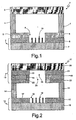
- Figure 1 shows a schematic view of a known Spindt-type cold cathode triode 1 including a cathode structure 2; an anode electrode 3 spaced from the cathode structure 2 by means of lateral spacers 4; and a control grid 5 integrated in the cathode structure 2.
- the cathode structure 2 with the integrated control grid 5 and the anode electrode 3 are formed separately and then bonded together with the interposition of the lateral spacers 4.
- the anode electrode 3 is made up of a first conductive substrate functioning as an anode, while the cathode structure 2 is a multilayer structure including a second conductive substrate 7; an insulating layer 8 arranged between the second conductive substrate 7 and the grid 5; a recess 9 formed to penetrate the grid 5 and the insulating layer 8 sq as to expose a surface of the second conductive substrate 7; and Spindt-type emitting tips 10 formed in the recess 9 in ohmic contact with the second conductive substrate 7 and functioning as a cathode.
- the main objective of present invention is therefore to provide an innovative topographical configuration of cold cathode vacuum tubes and an innovative manufacturing method which allow the aforementioned drawbacks to be at least overcome.
- the present invention relates to a high frequency, cold cathode, triode-type, field-emitter vacuum tube and to a process for manufacturing the same, as defined in the appended claims.
- the present invention achieves the aforementioned objective by varying the typical topography of the vacuum tube, and in particularly by forming the control grid over the anode, instead of over the cathode as in the known Spindt-type vacuum tubes, and then assembling the anode and the control grid formed thereover with the cathode, which is always manufactured separately from the anode (and the grid), with the interposition of spacers.
- an additional insulating layer is formed between the anode and the grid to cover also the side walls of the grid, thereby further reducing leakage currents.
- WO 00/24027 A discloses a field emission device including a cathode plate having electron emitters, an anode plate having a phosphor activated by electrons emitted by electron emitters, and a vacuum bridge focusing structure for focusing electrons emitted by electron emitters.
- Vacuum bridge focusing structure has landings, which are attached to anode plate, and further has bridges, which extend above and beyond landings to provide a self-supporting structure that is spaced apart from anode plate.
- JP 2006 253100 A discloses an electron/ion source device, which suppresses effects on the functions of the device and controls the focusing of electrons/ions with a relatively simple structure.
- a permittivity modulation part having regions of different permittivities is provided at least in a part between an anode and a cathode.
- JP 2006 024516 A discloses a picture display device in which display quality is improved by suppressing an unnecessary light emission.
- a plurality of spacers which support atmospheric pressure load to act on the first and the second plate board, and a supporting substrate are installed.
- the supporting substrate has a plurality of electron beam penetrating holes respectively confronting with the electron emitting sources, and an insulating layer in which the outer face is covered.
- a voltage impressing part which impresses a desired voltage on a fluorescent layer is installed.
- a resistance is connected between the supporting substrate and the voltage impressing part, and this resistance has a smaller resistance value than that of the insulating layer.
- JP 2006 128083 A discloses a field emission type image display device in which high illuminance is realized without increasing anode voltage and high resolution is realized by suppressing occurrence of cross talk between picture elements caused by excited light from the phosphor layer.
- the field emission type image display device is constructed of a filed emission electron source arranged in a vacuum container and a phosphor screen which is arranged in the vacuum container opposed to the field emission electron source and has a plurality of recessed portions on the face opposed to the field emission electron source and in which a phosphor layer is formed in the recessed portions.
- the phosphor layer is made to emit light by the collision of electrons emitted from the field emission electron source, and picture is displayed.
- the inner wall face of the recessed portion is widened in taper shape from the bottom face side toward the opening face side, and the adjoining recessed portions are divided by rib structures made of a material having optical absorption function to the light of emission wavelength.
- the phosphor layer is formed on almost whole surfaces of the bottom face and the inner wall face of the recessed portion 11.
- Figure 2 shows a schematic view of a high frequency cold cathode triode-type field-emitter vacuum tube in accordance with an embodiment of the present invention.
- the cold cathode triode-type field-emitter vacuum tube designated by 11, includes a cathode structure 12; an anode structure 13 spaced from the cathode structure 12 by means of lateral spacers 14; and a control grid 15 integrated in the anode structure 13.
- the cathode structure 12 and the anode structure 13 with the integrated grid 15 are formed separately and then bonded together with the interposition of the lateral spacers 14.
- the cathode structure 12 is a multilayer structure including a first conductive substrate 16; a first insulating layer 17 formed on the first conductive substrate 16; a recess 18 formed to penetrate the first insulating layer 17 so as to expose a surface of the first conductive substrate 16; and emitting tips 19, in the form of carbon nanotubes, nanowires or Spindt-type tips, formed in the recess 18 in ohmic contact with the first conductive substrate 16, and functioning as a cathode.
- the anode structure 13 is a multilayer structure including a second conductive substrate 20 functioning as an anode; a second insulating layer 21 formed between the second conductive substrate 20 and the grid 15; a. double recess structure including a wide recess 23 formed to penetrate the grid 15 so as to expose a surface of the second insulating layer 21, and a narrow recess 24 formed in the wide recess 23 to penetrate the second insulating layer 21 so as to expose a surface of the second conductive substrate 20; and a third insulating layer 22 formed between the grid 15 and the lateral spacers 14 and covering also the side walls of the grid 15.
- Recesses 18, 23 and 24 are vertically aligned in such a manner that the emitting tips 19 face the exposed surface of the second conductive substrate 20, and the lateral spacers 14 are arranged outside the recesses 18, 23 and 24 so that the recesses 18, 23 and 24 and the emitting tips 19 are arranged between the lateral spacers 14.
- FIGs 3a-3l are sectional views of a semiconductor wafer during successive steps of the manufacture of the cathode structure 12 of Figure 2 , in accordance with an embodiment of the present invention, where same reference numerals designate same elements. Additionally, for the sake of simplicity, the following description will refer to the manufacture of two adjacent cathode structures 12, the manufacture of an array of cathode structures 12 simply requiring the use of lithographical masks in which the same structure is repeated.
- a masking layer 30, made for example of photoresist is formed, for example by deposition, on the insulating layer 17 ( Figure 3b ), then patterned, in the example considered by a masked UV exposure, designated by 31 ( Figure 3c ), and subsequently developed, so forming a mask 32 with apertures which expose selective portions of the insulating layer 17 ( Figure 3d ).
- the apertures are advantageously in the form of strips extending in a perpendicular direction to the sheet, are spaced from one another by approximately 5-20 ⁇ m, and have a width of 1-5 ⁇ m.
- each trench 33 defines a respective recess 18 in the insulating layer 17 ( Figure 2 ), where the emitting tips 19 will then be formed.
- the mask 32 is removed ( Figure 3f ) and vertically aligned carbon nanotubes emitting tips 19 ( Figure 3h ) are synthesized in the trenches 33 by depositing a 20nm-thick catalyst layer 35 (for example Fe or Ni) on the wafer by casting (the solution that may for example be used is Fe(NO 3 ) 3 ⁇ 9H 2 O in acetone) ( Figure 3g ).
- a 20nm-thick catalyst layer 35 for example Fe or Ni
- the solution that may for example be used is Fe(NO 3 ) 3 ⁇ 9H 2 O in acetone
- the mask 32 is not removed and used as a mask for the 20nm-thick catalyst layer 35, which is deposited on the wafer by sputtering ( Figure 3i ), and then removed, by using a lift-off technique, from the insulating columns 34 and the lateral walls of the trenches 33 ( figure 3l ).
- a further lithographic step may be provided to pattern the catalyst layer 35 in the trenches 33.
- the selectivity is guaranteed by the reduction of the Fe(NO 3 ) 3 in the reaction chamber, which reduction takes place only in the areas of the conductive substrate 16 exposed via the lithographic process, while if the carbon nanotubes emitting tips 19 are grown as previously described with reference to Figures 3i and 3l , namely via a catalyst deposited by sputtering, the selectivity is guaranteed by the lithographic process which defines areas on which the catalyst is present, which catalyst, during the synthesis, has to be clustered.
- Figures 4a-4m are sectional views of a semiconductor wafer during successive steps of the manufacture of the anode structure 13 of Figure 2 , in accordance with an embodiment of the present invention, where same reference numerals designate same elements. Additionally, for the sake of simplicity, the following description will refer to the manufacture of two adjacent anode structures 13, the manufacture of an array of anode structures 13 simply requiring the use of lithographical masks in which the same structure in repeated.
- a first masking layer 36 for example made of photoresist
- the apertures are advantageously in the form of strips extending in a perpendicular direction to the sheet, are spaced from one another by approximately 5-50 ⁇ m, and have a width of 1-5 ⁇ m.
- first mask 38 exposed portions of the insulating layer 21 are dry or wet etched, so forming trenches 39 in the insulating layer 21, which trenches are laterally delimited by insulating columns 40, extend in depth as far as the conductive substrate 20, and have a shape, a width and a spacing corresponding to that of the apertures of the first mask 38 ( Figure 4e ).
- a second masking layer 41 for example made of photoresist, is formed, in the example considered by deposition, which completely fills the trenches 39 and covers the insulating columns 40 ( Figure 4g ).
- the second masking layer 41 is then patterned, in the example considered by a masked UV exposure, designated by 42 ( Figure 4h ), so as to expose only the portions of the second masking layer 41 on the insulating columns 40, while leaving covered the portions of the second masking layer 41 on the trenches 39 ( Figure 4h ), and subsequently developed, so as to form a third mask 43 which completely covers bottom and lateral walls of the trenches 39 and also partly extends on the insulating columns 40 for about 1-50 ⁇ m ( Figure 4i ).
- a 50-500 nm-thick metal grid layer 44 is then formed, for example by deposition, on the wafer, so as to completely fill the trenches 39 and cover the insulating columns 40 ( Figure 4l ), and then removed, using a lift-off process, all over the entire surface of the wafer, except on the areas of the insulating columns 40 exposed by the third mask 43, thus forming the grid 15.
- a grid insulating layer 22 having the purpose of covering the grid 15 to prevent a shortcircuit of the grid with the emitting tips 19, is formed, in the example considered by oxidation, on the grid 15 by anodizing, thus obtaining the structure shown in Figure 4m , where the internal vertical sides of the grid remain spaced out from the internal vertical sides of the insulating columns 40 of 1-20 ⁇ m, thus significantly limiting the leakage currents because the emitted electrons are not collected by the grid 15 which is covered by the oxide.
- the grid 15 has to be dimensioned consistently with the structure alignment process, which may vary depending on the applications which the cold cathode triode-type field-emitter vacuum tube 11 is designed for.
- the cathode structure 12 and the anode structure 13 with integrated grid 15 formed as described above with references to Figures 3 and 4 are aligned and bonded together via the interposition of the lateral spacers 14, and creating the vacuum therebetween (vacuum bonding).
- the function of the lateral spacers 14 is that of allowing an electrical insulation between the cathode structure 12 and the anode structure 13 to be created and an effective vacuum bonding to be made.
- standard wafer-to-wafer vacuum bonding techniques may be used to join the cathode structure 12 and the anode structure 13, including anodic bonding, glass frit bonding, eutectic bonding, solder bonding, reactive bonding and fusion bonding.
- One of the main problems of this type of packing techniques is linked to the pressure that is reached in the cavity between the cathode structure 12 and the anode structure 13.
- the pressure in the cavity reaches values 100-400 Torr due to oxygen generation
- the pressure in the cavity reaches values of 2 Torr due to gas desorption, which pressure may be reduced to 1 Torr if the wafers are heated up before assembly. Therefore, what happens is that while it is possible to obtain pressures below ⁇ Torr by using vacuum wafer bonding techniques, material desorption that happens as a result of the bonding (or assembly), the final pressure is always relatively high.
- the second masking layer 41 is patterned, in the example considered by a masked UV exposure, designated by 45, so as to expose only a portion of the second masking layer 41 on one trench 39, while leaving covered the remaining portions of the second masking layer 41 on the insulating columns 40 and the other trench 39 ( Figure 5h ), and subsequently developed, so as to form a third mask 46 which completely covers the insulating columns 40 and the bottom and lateral walls of the trench 39 that was not exposed during the masked UV exposure, while leaving exposed only the bottom and lateral walls of the trench 39 that was exposed during the masked UV exposure ( Figure 5i ).
- a metal getter layer 47 having a thickness in the range of microns is formed, for example by deposition, on the wafer ( Figure 5l ), and then removed, using a lift-off process, all over the entire surface of the wafer, except on the trench 39 that was not covered by the third mask 46 ( Figure 5m ).
- a third masking layer 48 for example made of photoresist, is then formed, in the example considered by deposition, on the wafer so as to completely fill the trenches 39 and cover the insulating columns 40, and then patterned, in the example considered by a masked UV exposure, designated by 49, so as to expose only portions of the third masking layer 48 on the insulating columns 40, while leaving covered portions of the third masking layer 48 on the trenches 39, and in particular on the getter layer 47 ( Figure 5n ).
- the third masking layer 48 is then developed so as to form a fourth mask 50 which completely covers the trench 39 that contains the getter 47 and also partly extends on the adjacent insulating columns 40 for about 1-50 ⁇ m, as well as completely covers the bottom and lateral walls of the other trench 39 that does not contain the getter 47 and also partly extends on the adjacent insulating columns 39 for about 1-50 mm ( Figure 5o ).
- a 50-500 nm-thick metal grid layer 44 is then formed, for example by deposition, on the wafer ( Figure 5p ), and then removed, using a lift-off process, all over the entire surface of the wafer, except on the area of the insulating columns 39 exposed by the fourth mask 50, thus forming the grid 15.
- a grid insulating layer 22, having the purpose of covering the grid to prevent a shortcircuit of the grid with the emitting tips 19, is formed, in the example considered by oxidation, on the grid 15 by anodizing, thus obtaining the structure shown in Figure 5q , where the internal vertical sides of the grid remain spaced out from the internal vertical sides of the insulating columns 39 of 1-50 ⁇ m, thus significantly limiting the leakage currents.
- the grid 15 and the getter 47 have, in top view, a ring pattern of the type show in Figure 6 , where the grid 15 is not visible because completely covered by the grid insulating layer 22.
- the anode structure 13 with integrated grid 15 and getter 47 is bonded to the cathode structure 12, so forming the cold cathode triode-type field-emitter vacuum tube 11' shown in Figure 7 , wherein the left part is identical to that shown in Figure 2 , and the right part is structurally similar to the left part, namely it includes a double recess structure including a wide recess 51 formed to penetrate the grid 15 so as to expose a surface of the second insulating layer 21, and a narrow recess 52 formed in the wide recess 51 to penetrate the second insulating layer 21 so as to expose a surface of the second conductive substrate 20, wherein the wide and narrow recesses. 51, 52 are separated from the wide and narrow recesses 23, 24 by a lateral spacer 14, and wherein the getter 47 is formed in the narrow recess 52.
- the thickness of the various layers of the field-emitter vacuum tube according to the present invention and the various steps of the respective manufacturing process are only indicative and may be varied according to specific necessity.
Landscapes
- Cold Cathode And The Manufacture (AREA)
- Cathode-Ray Tubes And Fluorescent Screens For Display (AREA)
Description
- The present invention relates in general to a micro/nanometrical device belonging to the family of semiconductor vacuum tubes for high frequency applications, and more particularly to a high frequency, cold cathode, triode-type, field-emitter vacuum tube and to a process for manufacturing the same.
- As is known, in the last thirty years, and in particular after the publication by Charles Spindt of his first article on the manufacture of cold cathode vacuum tubes (C. A. Spindt et al., Physical properties of thin-film field emission cathodes with molybdenum cones, Journal of Applied Physics, vol. 47, Dec. 1976, pages 5248-5263), there has been a renewed interest in the manufacture of high frequency, wide band, radiation insensitive vacuum tubes. This renewed interest is justified by the fact that this type of electronic devices, which, for generating an electron beam, exploit the field emission phenomenon instead of the thermionic phenomenon exploited by the conventional, old generation vacuum tubes, lend themselves to an ever increasing miniaturization.
- In fact, the conventional vacuum tubes suffered from limitations due to the use of a thermionic cathode for electron emission, which cathode, in order to emit electrons, had to reach high operating temperatures of about 800 to 1200°C, with consequent problems linked to the management of the electrical power necessary to operate the vacuum tube (in a tube operating at low electrical power, namely less than 10 W, the electrical power necessary to heat up the cathode may be higher than the operating one) and of the so-called heating-up time (thermionic effect initiation time), and also linked to the stabilization of the control grid, which, in high frequency applications, was too close to the cathode (<25µm) (see for example C. Bower, W. Zhu, D. Shalom, D. Lopez, G. P. Kochanski, P. L. Gammel, S. Jin, A micromachined vacuum triode using a carbon nanotube cold cathode, IEEE transactions on Electron Devices, Vol. 49, Aug. 2002, pages 1478-1483).
- On the contrary, the vacuum tube with a field emission array (FEA) cathode proposed by Spindt, generally known as Spindt Cathode, allowed the advantages provided by the vacuum electronics to be enjoyed, namely the property of the electrons of reaching higher speeds in the vacuum than in a semiconductor material. All these advantages are achieved with a substantially zero heating-up time, and with the possibility of arranging the control grid close to the cathode without having instability problems due to the heat of the electrodes, thus allowing higher operating frequencies to be reached (nominally from GHz to THz) and lower electrical power to initiate the electron generation process than necessary in thermionic tubes.
- In particular, Spindt cathodes consist of microfabricated metal field emitter cones or tips formed on a conductive substrate. Each emitter has its own concentric aperture in an accelerating field generated by a gate electrode, also known as control grid, which is isolated from the substrate and the emitters by a silicon dioxide layer. With individual tips capable of producing several tens of microamperes, large arrays can theoretically produce large emission current densities.
- Performance of Spindt cathodes are heavily limited by the destruction of the emitting tips due to their material wear, and for this reason many efforts have been spent worldwide in searching innovative materials for the production of the emitting tips.
- In particular, the Spindt structure was improved by considering carbon nanotubes (CNTs) as cold cathode emitters (see for example S. Iijima, Helical microtubules of graphitic carbon, Nature, 1991, volume 354, pages 56-58, or W. Heer, A. Chatelain, D. Ugarte, A carbon nanotube field-emission electron source, Science, 1995, volume 270, number 5239, pages 1179-1180). Carbon nanotubes are perfectly graphitized, cylindrical tubes that can be produced with diameters ranging from about 2 to 100 nm, and lengths of several microns using different production processes. CNTs may be rated among the best emitters in nature (see for example J. M. Bonard, J.-P. Salvetat, T. Stöckli, L. Forrò, A. Châtelain, Field emission from carbon nanotubes: perspectives for applications and clues to the emission mechanism, Applied Physics A, 1999, volume 69, pages 245-254) and are ideal field emitters in a Spindt-type device, so many efforts have been spent worldwide in studying their field emission properties.
-
Figure 1 shows a schematic view of a known Spindt-typecold cathode triode 1 including acathode structure 2; ananode electrode 3 spaced from thecathode structure 2 by means oflateral spacers 4; and acontrol grid 5 integrated in thecathode structure 2. Thecathode structure 2 with the integratedcontrol grid 5 and theanode electrode 3 are formed separately and then bonded together with the interposition of thelateral spacers 4. Theanode electrode 3 is made up of a first conductive substrate functioning as an anode, while thecathode structure 2 is a multilayer structure including a secondconductive substrate 7; aninsulating layer 8 arranged between the secondconductive substrate 7 and thegrid 5; arecess 9 formed to penetrate thegrid 5 and theinsulating layer 8 sq as to expose a surface of the secondconductive substrate 7; and Spindt-type emitting tips 10 formed in therecess 9 in ohmic contact with the secondconductive substrate 7 and functioning as a cathode. - The Applicant has noticed that the topographic configuration of known Spindt-type vacuum tubes, in which the control grid is formed over the cathode, suffers from different problems, and in particular:
- manufacture of emitting tips integrated with the control grid typically requires a complex technological process because it is necessary to place the emitting cathode within a multilayer structure (conductive substrate - insulating oxide - grid metal), and this process typically requires a high number of technological steps, the complexity of which is due to the difficulty of integrating different technologies. For emitting cathodes made up of carbon nanotubes it is for example necessary to study the technological steps relating to the manufacture of the substrate, and hence typically the materials used for the manufacture and the topography of the structures, so as to allow the subsequent growth of the carbon nanotubes by using the typical techniques used for this purpose (HF-CVD, PE-CVD, laser ablation);
- in devices with emitting tips that come out from an opening in the insulating layer, for example when carbon nanotubes are used as emitting tips, proximity of the control grid to the cathode may cause a short circuit between the control grid and the emitting tips, with consequent malfunctioning of the device;
- the metal grid absorbs a non-neglectable part of the electrons emitted by the cathode (∼ 10%, see for example Y. M. Wong , W. P. Kang , J. L. Davidson, B. K. Choi, W. Hofmeister, J. H. Huang, Field emission triode amplifier utilizing aligned carbon nanotubes, Diamond and related materials 2005, ), so making the device performance worse; and
- the operating frequency of this type of device is heavily limited by the parasitic capacitance between the grid and the cathode. In fact, assuming that the grid and the cathode may be modeled as two flat and parallel planes, the parasitic capacitance is C=ε0Cr(A/d), where c0 is the vacuum permittivity, εr is the relative permittivity of the insulating material between the cathode and the grid, A is the area of the grid, and d is the distance between the cathode and the grid. From the foregoing, it is evident that the operating frequency of this type of device is heavily dependent on the topographic characteristics of the device itself.
- The main objective of present invention is therefore to provide an innovative topographical configuration of cold cathode vacuum tubes and an innovative manufacturing method which allow the aforementioned drawbacks to be at least overcome.
- This objective is achieved by the present invention in that it relates to a high frequency, cold cathode, triode-type, field-emitter vacuum tube and to a process for manufacturing the same, as defined in the appended claims.
The present invention achieves the aforementioned objective by varying the typical topography of the vacuum tube, and in particularly by forming the control grid over the anode, instead of over the cathode as in the known Spindt-type vacuum tubes, and then assembling the anode and the control grid formed thereover with the cathode, which is always manufactured separately from the anode (and the grid), with the interposition of spacers. During the formation of the grid over the anode, an additional insulating layer is formed between the anode and the grid to cover also the side walls of the grid, thereby further reducing leakage currents. -
WO 00/24027 A -
JP 2006 253100 A -
JP 2006 024516 A -
JP 2006 128083 A recessed portion 11. - For a better understanding of the present invention, preferred embodiments, which are intended purely by way of example and are not to be construed as limiting, will now be described with reference to the attached drawings (all not to scale), wherein:
-
Figure 1 shows a schematic view of a known Spindt-type cold cathode triode; -
Figure 2 shows a schematic view of a high frequency cold cathode triode-type field-emitter vacuum tube in accordance with an embodiment of the present invention; -
Figures 3a-3l are lateral sectional views of a semiconductor wafer during successive steps of the manufacture of a cathode structure of the Spindt-type cold cathode field-emitter triode ofFigure 2 , in accordance with an embodiment of the present invention; -
Figures 4a-4m are lateral sectional views of a semiconductor wafer during successive steps of the manufacture of an anode structure of the Spindt-type cold cathode field-emitter triode ofFigure 2 , in accordance with an embodiment of the present invention; -
Figures 5a-5q are sectional views of a semiconductor wafer during successive steps of the manufacture of an anode structure, provided with a getter material, of a Spindt-type cold cathode field-emitter triode in accordance with an embodiment of the present invention; -
Figure 6 is a top view of an anode structure, provided with a getter material, of a Spindt-type cold cathode field-emitter triode in accordance with an embodiment of the present invention; and -
Figure 7 shows a schematic view of a Spindt-type cold cathode triode-type field-emitter vacuum tube provided with a getter material, in accordance with an embodiment of the present invention. - The following discussion is presented to enable a person skilled in the art to make and use the invention. Various modifications to the embodiments will be readily apparent to those skilled in the art, and the generic principles herein may be applied to other embodiments and applications without departing from the spirit and scope of the present invention. Thus, the present invention is not intended to be limited to the embodiments shown, but is to be accorded the widest scope consistent with the principles and features disclosed herein.and defined in the attached claims.
-
Figure 2 shows a schematic view of a high frequency cold cathode triode-type field-emitter vacuum tube in accordance with an embodiment of the present invention. - The cold cathode triode-type field-emitter vacuum tube, designated by 11, includes a
cathode structure 12; ananode structure 13 spaced from thecathode structure 12 by means oflateral spacers 14; and acontrol grid 15 integrated in theanode structure 13. Thecathode structure 12 and theanode structure 13 with theintegrated grid 15 are formed separately and then bonded together with the interposition of thelateral spacers 14. - In particular, the
cathode structure 12 is a multilayer structure including a firstconductive substrate 16; a first insulatinglayer 17 formed on the firstconductive substrate 16; arecess 18 formed to penetrate the first insulatinglayer 17 so as to expose a surface of the firstconductive substrate 16; and emittingtips 19, in the form of carbon nanotubes, nanowires or Spindt-type tips, formed in therecess 18 in ohmic contact with the firstconductive substrate 16, and functioning as a cathode. - The
anode structure 13 is a multilayer structure including a secondconductive substrate 20 functioning as an anode; a second insulatinglayer 21 formed between the secondconductive substrate 20 and thegrid 15; a. double recess structure including awide recess 23 formed to penetrate thegrid 15 so as to expose a surface of the second insulatinglayer 21, and anarrow recess 24 formed in thewide recess 23 to penetrate the second insulatinglayer 21 so as to expose a surface of the secondconductive substrate 20; and a third insulatinglayer 22 formed between thegrid 15 and thelateral spacers 14 and covering also the side walls of thegrid 15. -
Recesses tips 19 face the exposed surface of the secondconductive substrate 20, and thelateral spacers 14 are arranged outside therecesses recesses tips 19 are arranged between thelateral spacers 14. -
Figures 3a-3l are sectional views of a semiconductor wafer during successive steps of the manufacture of thecathode structure 12 ofFigure 2 , in accordance with an embodiment of the present invention, where same reference numerals designate same elements. Additionally, for the sake of simplicity, the following description will refer to the manufacture of twoadjacent cathode structures 12, the manufacture of an array ofcathode structures 12 simply requiring the use of lithographical masks in which the same structure is repeated. - With reference to
Figures 3a-3l , a 1-5 µm-thickinsulating layer 17 made for example of silicon dioxide (SiO2), is formed, in the example considered by oxidation, on a 300-µm thickconductive substrate 16 made for example of monocrystalline silicon (Si) (Figure 3a ). Then amasking layer 30, made for example of photoresist, is formed, for example by deposition, on the insulating layer 17 (Figure 3b ), then patterned, in the example considered by a masked UV exposure, designated by 31 (Figure 3c ), and subsequently developed, so forming amask 32 with apertures which expose selective portions of the insulating layer 17 (Figure 3d ). The apertures are advantageously in the form of strips extending in a perpendicular direction to the sheet, are spaced from one another by approximately 5-20 µm, and have a width of 1-5 µm. - Using the
mask 32, exposed portions of the insulatinglayer 17 are wet or dry etched, so formingtrenches 33 in the insulatinglayer 17, whichtrenches 33 are laterally delimited by insulatingcolumns 34, extend in depth as far as theconductive substrate 16, and have a shape, a width and a spacing corresponding to that of the apertures of the mask 32 (Figure 3e ). Additionally, eachtrench 33 defines arespective recess 18 in the insulating layer 17 (Figure 2 ), where the emittingtips 19 will then be formed. - Then, in a first embodiment shown in
Figures 3f, 3g and 3h , themask 32 is removed (Figure 3f ) and vertically aligned carbon nanotubes emitting tips 19 (Figure 3h ) are synthesized in thetrenches 33 by depositing a 20nm-thick catalyst layer 35 (for example Fe or Ni) on the wafer by casting (the solution that may for example be used is Fe(NO3)3·9H2O in acetone) (Figure 3g ). - In a second, alternative embodiment shown in
Figures 3i and 3l , themask 32 is not removed and used as a mask for the 20nm-thick catalyst layer 35, which is deposited on the wafer by sputtering (Figure 3i ), and then removed, by using a lift-off technique, from the insulatingcolumns 34 and the lateral walls of the trenches 33 (figure 3l ). - In a third, alternative embodiment (not shown), a further lithographic step may be provided to pattern the
catalyst layer 35 in thetrenches 33. - If the carbon
nanotubes emitting tips 19 are grown as previously described with reference toFigures 3f and 3g , namely from a catalyst in solution deposited by casting, the selectivity is guaranteed by the reduction of the Fe(NO3)3 in the reaction chamber, which reduction takes place only in the areas of theconductive substrate 16 exposed via the lithographic process, while if the carbonnanotubes emitting tips 19 are grown as previously described with reference toFigures 3i and 3l , namely via a catalyst deposited by sputtering, the selectivity is guaranteed by the lithographic process which defines areas on which the catalyst is present, which catalyst, during the synthesis, has to be clustered. -
Figures 4a-4m are sectional views of a semiconductor wafer during successive steps of the manufacture of theanode structure 13 ofFigure 2 , in accordance with an embodiment of the present invention, where same reference numerals designate same elements. Additionally, for the sake of simplicity, the following description will refer to the manufacture of twoadjacent anode structures 13, the manufacture of an array ofanode structures 13 simply requiring the use of lithographical masks in which the same structure in repeated. - With reference to
Figures 4a-4m , an insulatinglayer 21, made for example of silicon dioxide (SiO2) and having a thickness from some microns to some tens of microns, is formed, in the example considered by oxidation, on a 300-µm thickconductive substrate 20 made for example of monocrystalline silicon (Si) (Figure 4a ). Then afirst masking layer 36, for example made of photoresist, is formed, for example by deposition, on the insulating layer 21 (Figure 4b ), then patterned, in the example considered by a masked UV exposure, designated by 37 (Figure. 4c ), and subsequently developed, so as to form afirst mask 38 with apertures which expose selective portions of the insulating layer 21 (Figure 4d ). The apertures are advantageously in the form of strips extending in a perpendicular direction to the sheet, are spaced from one another by approximately 5-50 µm, and have a width of 1-5 µm. - Using the
first mask 38, exposed portions of the insulatinglayer 21 are dry or wet etched, so formingtrenches 39 in the insulatinglayer 21, which trenches are laterally delimited by insulatingcolumns 40, extend in depth as far as theconductive substrate 20, and have a shape, a width and a spacing corresponding to that of the apertures of the first mask 38 (Figure 4e ). - Then, the
first mask 38 is removed (Figure 4f ) and asecond masking layer 41, for example made of photoresist, is formed, in the example considered by deposition, which completely fills thetrenches 39 and covers the insulating columns 40 (Figure 4g ). Thesecond masking layer 41 is then patterned, in the example considered by a masked UV exposure, designated by 42 (Figure 4h ), so as to expose only the portions of thesecond masking layer 41 on the insulatingcolumns 40, while leaving covered the portions of thesecond masking layer 41 on the trenches 39 (Figure 4h ), and subsequently developed, so as to form athird mask 43 which completely covers bottom and lateral walls of thetrenches 39 and also partly extends on the insulatingcolumns 40 for about 1-50 µm (Figure 4i ). - A 50-500 nm-thick metal grid layer 44 is then formed, for example by deposition, on the wafer, so as to completely fill the
trenches 39 and cover the insulating columns 40 (Figure 4l ), and then removed, using a lift-off process, all over the entire surface of the wafer, except on the areas of the insulatingcolumns 40 exposed by thethird mask 43, thus forming thegrid 15. Finally, agrid insulating layer 22, having the purpose of covering thegrid 15 to prevent a shortcircuit of the grid with the emittingtips 19, is formed, in the example considered by oxidation, on thegrid 15 by anodizing, thus obtaining the structure shown inFigure 4m , where the internal vertical sides of the grid remain spaced out from the internal vertical sides of the insulatingcolumns 40 of 1-20 µm, thus significantly limiting the leakage currents because the emitted electrons are not collected by thegrid 15 which is covered by the oxide. As a general rule, as the dimension of thegrid 15 depends on the grid-to-trench and grid-to-grid distances, thegrid 15 has to be dimensioned consistently with the structure alignment process, which may vary depending on the applications which the cold cathode triode-type field-emitter vacuum tube 11 is designed for. - The
cathode structure 12 and theanode structure 13 withintegrated grid 15 formed as described above with references toFigures 3 and4 are aligned and bonded together via the interposition of thelateral spacers 14, and creating the vacuum therebetween (vacuum bonding). The function of thelateral spacers 14 is that of allowing an electrical insulation between thecathode structure 12 and theanode structure 13 to be created and an effective vacuum bonding to be made. In particular, standard wafer-to-wafer vacuum bonding techniques may be used to join thecathode structure 12 and theanode structure 13, including anodic bonding, glass frit bonding, eutectic bonding, solder bonding, reactive bonding and fusion bonding. - One of the main problems of this type of packing techniques is linked to the pressure that is reached in the cavity between the
cathode structure 12 and theanode structure 13. For example, in the anodic bonding the pressure in the cavity reaches values 100-400 Torr due to oxygen generation, while in the solder bonding the pressure in the cavity reaches values of 2 Torr due to gas desorption, which pressure may be reduced to 1 Torr if the wafers are heated up before assembly. Therefore, what happens is that while it is possible to obtain pressures below µTorr by using vacuum wafer bonding techniques, material desorption that happens as a result of the bonding (or assembly), the final pressure is always relatively high. - Since a high quality of vacuum is necessary for a good operation of the field-
emitter vacuum tube 11, according to another aspect of the present invention, formation of a region containing a particularly reactive material such as Ba, Al, Ti, Zr, V, Fe, commonly known as getter, allows, when appropriately activated, molecules desorbed during the bonding to be captured. For a detailed description of getter material reference may be made to Douglas R. Sparks, S. Massoud-Ansari, and Nader Najafi, Chip-Level Vacuum Packaging of Micromachines Using NanoGetters, IEEE transactions on advanced packaging, volume 26, , and Yufeng Jin, Zhenfeng Wang, Lei Zhao, Peck Cheng Lim, Jun Wei and Chee Khuen Wong, Zr/V/Fe thick film for vacuum packaging of MEMS, Journal of Micromechanics and Microengineering, . - Introduction of the getter material in the field-emitter vacuum tube, hereinafter designated by 11', may be made by an additional step in the process of manufacture of the
anode structure 13, as shown inFigures 5a to 5q , whereFigures 5a to 5g are the same asFigures 4a to 4g and hence will not be described again. - With reference to
Figures 5a to 5q , once thefirst mask 38 has been removed (Figure 5f ) and thesecond masking layer 41 has been formed (Figure 5g ), thesecond masking layer 41 is patterned, in the example considered by a masked UV exposure, designated by 45, so as to expose only a portion of thesecond masking layer 41 on onetrench 39, while leaving covered the remaining portions of thesecond masking layer 41 on the insulatingcolumns 40 and the other trench 39 (Figure 5h ), and subsequently developed, so as to form athird mask 46 which completely covers the insulatingcolumns 40 and the bottom and lateral walls of thetrench 39 that was not exposed during the masked UV exposure, while leaving exposed only the bottom and lateral walls of thetrench 39 that was exposed during the masked UV exposure (Figure 5i ). - Then, a
metal getter layer 47 having a thickness in the range of microns is formed, for example by deposition, on the wafer (Figure 5l ), and then removed, using a lift-off process, all over the entire surface of the wafer, except on thetrench 39 that was not covered by the third mask 46 (Figure 5m ). Athird masking layer 48, for example made of photoresist, is then formed, in the example considered by deposition, on the wafer so as to completely fill thetrenches 39 and cover the insulatingcolumns 40, and then patterned, in the example considered by a masked UV exposure, designated by 49, so as to expose only portions of thethird masking layer 48 on the insulatingcolumns 40, while leaving covered portions of thethird masking layer 48 on thetrenches 39, and in particular on the getter layer 47 (Figure 5n ). Thethird masking layer 48 is then developed so as to form afourth mask 50 which completely covers thetrench 39 that contains thegetter 47 and also partly extends on the adjacent insulatingcolumns 40 for about 1-50 µm, as well as completely covers the bottom and lateral walls of theother trench 39 that does not contain thegetter 47 and also partly extends on the adjacent insulatingcolumns 39 for about 1-50 mm (Figure 5o ). - A 50-500 nm-thick metal grid layer 44 is then formed, for example by deposition, on the wafer (
Figure 5p ), and then removed, using a lift-off process, all over the entire surface of the wafer, except on the area of the insulatingcolumns 39 exposed by thefourth mask 50, thus forming thegrid 15. Finally, agrid insulating layer 22, having the purpose of covering the grid to prevent a shortcircuit of the grid with the emittingtips 19, is formed, in the example considered by oxidation, on thegrid 15 by anodizing, thus obtaining the structure shown inFigure 5q , where the internal vertical sides of the grid remain spaced out from the internal vertical sides of the insulatingcolumns 39 of 1-50 µm, thus significantly limiting the leakage currents. Preferably, thegrid 15 and thegetter 47 have, in top view, a ring pattern of the type show inFigure 6 , where thegrid 15 is not visible because completely covered by thegrid insulating layer 22. - Finally, the
anode structure 13 withintegrated grid 15 andgetter 47 is bonded to thecathode structure 12, so forming the cold cathode triode-type field-emitter vacuum tube 11' shown inFigure 7 , wherein the left part is identical to that shown inFigure 2 , and the right part is structurally similar to the left part, namely it includes a double recess structure including awide recess 51 formed to penetrate thegrid 15 so as to expose a surface of the second insulatinglayer 21, and anarrow recess 52 formed in thewide recess 51 to penetrate the second insulatinglayer 21 so as to expose a surface of the secondconductive substrate 20, wherein the wide and narrow recesses. 51, 52 are separated from the wide andnarrow recesses lateral spacer 14, and wherein thegetter 47 is formed in thenarrow recess 52. - The advantages of the field-emitter vacuum tube according to the present invention are evident from the foregoing. In particular:
- the integration of the
grid 15 in theanode structure 13 instead of in thecathode structure 12 prevents any shortcircuit between thegrid 15 and the emittingtips 19, and allows a simpler and highly reproducible manufacturing process to be obtained; - the additional insulating
layer 22 between thegrid 15 and thelateral spacers 14 and the fact that the internal vertical sides of thegrid 15 are spaced out from the internal vertical sides of the insulatinglayer 21 significantly reduce the leakage currents; and - the thickness of the
conductive substrate 20 and of the insulatinglayer 21 in theanode structure 13 allows a lower parasitic capacitance between theanode 20 and thegrid 15 to be obtained and consequently a higher operating frequency to be reached. - Finally, numerous modifications and variants can be made to the field-emitter vacuum tube according to the present invention, all falling within the scope of the invention, as defined in the appended claims.
- In particular, it may be appreciated by the skilled person that the thickness of the various layers of the field-emitter vacuum tube according to the present invention and the various steps of the respective manufacturing process are only indicative and may be varied according to specific necessity.
Claims (12)
- A cold cathode triode-type field-emitter vacuum tube (11; 11') including a cathode structure (12) and an anode structure (13) formed separately and bonded together with interposition of spacers (14), and a control grid (15) integrated in the anode structure (12); wherein the anode structure (13) includes a first conductive substrate (20), a first insulating layer (21) formed between the first conductive substrate (20) and the grid (15), a second insulating layer (22) formed between the grid (15) and the spacers (14), and a first recess structure (23, 24) formed to penetrate the second insulating layer (22), the grid (15) and the first insulating layer (21) so as to expose a surface of the first conductive substrate (20); wherein the first recess structure (23, 24) includes a first wider recess (23) formed to penetrate the second insulating layer (22) and the grid (15) so as to expose a surface of the first insulating layer (21), and a first narrower recess (24) formed in the first wider recess (23) to penetrate the first insulating layer (21) so as to expose a surface of the first conductive substrate (20); wherein the second insulating layer (22) is so formed to cover side walls of the grid (15) in the first wider recess (23); and wherein widths of the wider and narrower recesses (23, 24) and thickness of the second insulating layer (22) which covers side walls of the grid (15) in the first wider recess (23) are so sized that side walls of the first insulating layer (21) in the narrower recess (24) protrude beyond side walls of the second insulating layer (22) which covers side walls of the grid (15) in the wider recess (23).
- The field-emitter vacuum tube of claim 1, wherein the cathode structure (12) includes a second conductive substrate (16), a third insulating layer (17) formed on the second conductive substrate (16), a third recess (18) formed to penetrate the third insulating layer (17) so as to expose a surface of the second conductive substrate (16), and emitting tips (19) formed in the third recess (18) and in ohmic contact with the second conductive substrate (16).
- The field-emitter vacuum tube of claim 2, wherein the recesses (18, 23, 24) are vertically aligned in such a manner that the emitting tips (19) face the exposed surface of the first conductive substrate (20), and the spacers (14) are arranged outside the recesses (18, 23, 24) so that the recesses (18, 23, 24) and the emitting tips (19) are arranged between the spacers (14).
- The field-emitter vacuum tube of any one of the preceding claims, further including a second recess structure (51, 52) formed to penetrate the second insulating layer (22), the grid (15) and the first insulating layer (21) so as to expose a surface of the first conductive substrate (20); and a getter material (47) formed in the second recess structure (51, 52).
- The field-emitter vacuum tube of claim 4, wherein the second recess structure (51, 52) includes a second wider recess (51) formed to penetrate the second insulating layer (22) and the grid (15) so as to expose a surface of the first insulating layer (21), and a second narrower recess (52) formed in the second wider recess (51) to penetrate the first insulating layer (21) so as to expose a surface of the first conductive substrate (20); and wherein the getter material (47) is arranged in the second narrower recess (52).
- The field-emitter vacuum tube of claim 4 or 5, wherein the first recess structure (23, 24) is separated from the second recess structure (51, 52) by a spacer (14).
- A method of manufacturing a cold cathode triode-type field-emitter vacuum tube (11; 11'), including:• forming separately a cathode structure (12) and an anode structure (13);• forming a control grid (15) integrated in the anode structure (12); and• bonding together the cathode structure (12) and the anode structure (13) with interposition of spacers (14);wherein forming an anode structure (13) includes:• forming a first conductive substrate (20);• forming a first insulating layer (21) between the first conductive substrate (20) and the grid (15);• forming a second insulating layer (22) between the grid (15) and the spacers (14); and• forming a first recess structure (23, 24) to penetrate the second insulating layer (22), the grid (15) and the first insulating layer (21) so as to expose a surface of the first conductive substrate (20);wherein forming a first recess structure (23, 24) includes:• forming a first wider recess (23) to penetrate the second insulating layer (22) and the grid (15) so as to expose a surface of the first insulating layer (21); and• forming a first narrower recess (24) in the first wider recess (23) to penetrate the first insulating layer (21) so as to expose a surface of the first conductive substrate (20);wherein the second insulating layer (22) is formed to cover side walls of the grid (15) in the first wider recess (23);
and wherein the method further comprises:• sizing widths of the wider and narrower recesses (23, 24) and thickness of the second insulating layer (22) which covers side walls of the grid (15) in the first wider recess (23) so that side walls of the first insulating layer (21) in the narrower recess (24) protrude beyond side walls of the second insulating layer (22) which covers side walls of the grid (15) in the wider recess (23). - The method of claim 7, wherein forming a cathode structure (12) includes:• forming a second conductive substrate (16);• forming a third insulating layer (17) on the second conductive substrate (16);• forming a third recess (18) to penetrate the third insulating layer (17) so as to expose a surface of the second conductive substrate (16); and• forming emitting tips (19) in the third recess (18) and in ohmic contact with the second conductive substrate (16).
- The method of claim 8, wherein the recesses (18, 23, 24) are formed vertically aligned in such a manner that the emitting tips (19) face the exposed surface of the first conductive substrate (20), and the spacers (14) are arranged outside the recesses (18, 23, 24) so that the recesses (18, 23, 24) and the emitting tips (19) are arranged between the spacers (14).
- The method of any one of the preceding claims 7 to 9, further including:• forming a second recess structure (51, 52) to penetrate the second insulating layer (22), the grid (15) and the first insulating layer (21) so as to expose a surface of the first conductive substrate (20); and• forming a getter material (47) in the second recess structure (51, 52).
- The method of claim 10, wherein forming a second recess structure (51, 52) includes:• forming a second wider recess (51) to penetrate the second insulating layer (22) and the grid (15) so as to expose a surface of the first insulating layer (21); and• forming a second narrower recess (52) in the second wider recess (51) to penetrate the first insulating layer (21) so as to expose a surface of the first conductive substrate (20);and wherein the getter material (47) is formed in the second narrower recess (52).
- The method of claim 10 or 11, wherein the first recess structure (23, 24) is separated from the second recess structure (51, 52) by a spacer (14).
Applications Claiming Priority (1)
| Application Number | Priority Date | Filing Date | Title |
|---|---|---|---|
| PCT/IT2006/000883 WO2008081482A1 (en) | 2006-12-29 | 2006-12-29 | High frequency, cold cathode, triode-type, field-emitter vacuum tube and process for manufacturing the same |
Publications (3)
| Publication Number | Publication Date |
|---|---|
| EP2126953A1 EP2126953A1 (en) | 2009-12-02 |
| EP2126953B1 true EP2126953B1 (en) | 2013-02-27 |
| EP2126953B8 EP2126953B8 (en) | 2013-04-10 |
Family
ID=38038404
Family Applications (1)
| Application Number | Title | Priority Date | Filing Date |
|---|---|---|---|
| EP06842811.9A Not-in-force EP2126953B8 (en) | 2006-12-29 | 2006-12-29 | High frequency, cold cathode, triode-type, field-emitter vacuum tube and process for manufacturing the same |
Country Status (6)
| Country | Link |
|---|---|
| US (1) | US8040038B2 (en) |
| EP (1) | EP2126953B8 (en) |
| JP (1) | JP2010515217A (en) |
| CN (1) | CN101636810B (en) |
| TW (1) | TW200836225A (en) |
| WO (1) | WO2008081482A1 (en) |
Families Citing this family (9)
| Publication number | Priority date | Publication date | Assignee | Title |
|---|---|---|---|---|
| CN102097272B (en) * | 2011-01-10 | 2012-06-27 | 福州大学 | Triode structured field emission display (FED) with anode and grid on same substrate |
| US9853243B2 (en) | 2013-07-05 | 2017-12-26 | Industrial Technology Research Institute | Flexible display and method for fabricating the same |
| US9169117B1 (en) * | 2014-04-25 | 2015-10-27 | Taiwan Semiconductor Manufacturing Company Limited | MEMS device and method of forming the same |
| CN105529356B (en) * | 2016-02-24 | 2019-02-05 | 西安交通大学 | A Field Emission Transistor With Vertical Structure Cylindrical Conductive Channel |
| CN108242466B (en) * | 2016-12-26 | 2020-09-01 | 中国科学院苏州纳米技术与纳米仿生研究所 | Field emission device and manufacturing method thereof |
| SE540824C2 (en) * | 2017-07-05 | 2018-11-20 | Lightlab Sweden Ab | A field emission cathode structure for a field emission arrangement |
| RU2680347C1 (en) * | 2018-04-28 | 2019-02-19 | Сергей Николаевич Веревкин | Field triode |
| CN113555445A (en) * | 2020-04-23 | 2021-10-26 | 北京大学 | On-chip triode, manufacturing method thereof and integrated circuit |
| WO2025233814A1 (en) * | 2024-05-07 | 2025-11-13 | Nano-X Imaging Ltd | System and method for increasing operational lifetime of a field emission vacuum tube |
Family Cites Families (16)
| Publication number | Priority date | Publication date | Assignee | Title |
|---|---|---|---|---|
| US5075595A (en) * | 1991-01-24 | 1991-12-24 | Motorola, Inc. | Field emission device with vertically integrated active control |
| JP3232195B2 (en) * | 1994-07-15 | 2001-11-26 | 松下電工株式会社 | Electron-emitting device |
| RU2118011C1 (en) * | 1996-05-08 | 1998-08-20 | Евгений Инвиевич Гиваргизов | Autoemission triode, device built around it, and its manufacturing process |
| JPH10289677A (en) * | 1997-04-11 | 1998-10-27 | Mitsubishi Electric Corp | Flat panel display |
| US6137213A (en) * | 1998-10-21 | 2000-10-24 | Motorola, Inc. | Field emission device having a vacuum bridge focusing structure and method |
| KR100343205B1 (en) * | 2000-04-26 | 2002-07-10 | 김순택 | Field emission array using carbon nanotube and fabricating method thereof |
| JP4830217B2 (en) * | 2001-06-18 | 2011-12-07 | 日本電気株式会社 | Field emission cold cathode and manufacturing method thereof |
| TW511108B (en) | 2001-08-13 | 2002-11-21 | Delta Optoelectronics Inc | Carbon nanotube field emission display technology |
| JP3954002B2 (en) * | 2002-12-24 | 2007-08-08 | 韓國電子通信研究院 | Field emission display |
| JP2006079873A (en) * | 2004-09-08 | 2006-03-23 | National Institute For Materials Science | Deep UV solid state light emitting device |
| JP2005332735A (en) * | 2004-05-21 | 2005-12-02 | Ci Techno:Kk | Electron emitting device and manufacturing method thereof |
| JP2006024516A (en) | 2004-07-09 | 2006-01-26 | Toshiba Corp | Image display device |
| JP2006128083A (en) | 2004-09-29 | 2006-05-18 | Matsushita Toshiba Picture Display Co Ltd | Field emission type image display device |
| US20060066216A1 (en) * | 2004-09-29 | 2006-03-30 | Matsushita Toshiba Picture Display Co., Ltd. | Field emission display |
| JP2006253100A (en) | 2005-02-10 | 2006-09-21 | Sony Corp | ELECTRON / ION SOURCE DEVICE, ITS MANUFACTURING METHOD, DISPLAY DEVICE, AND ITS MANUFACTURING METHOD |
| JP4387988B2 (en) * | 2005-06-01 | 2009-12-24 | 富士重工業株式会社 | Light emitting device |
-
2006
- 2006-12-29 CN CN2006800569285A patent/CN101636810B/en not_active Expired - Fee Related
- 2006-12-29 WO PCT/IT2006/000883 patent/WO2008081482A1/en not_active Ceased
- 2006-12-29 EP EP06842811.9A patent/EP2126953B8/en not_active Not-in-force
- 2006-12-29 US US12/521,641 patent/US8040038B2/en not_active Expired - Fee Related
- 2006-12-29 JP JP2009543576A patent/JP2010515217A/en active Pending
-
2007
- 2007-12-31 TW TW096151539A patent/TW200836225A/en unknown
Also Published As
| Publication number | Publication date |
|---|---|
| EP2126953A1 (en) | 2009-12-02 |
| TW200836225A (en) | 2008-09-01 |
| US8040038B2 (en) | 2011-10-18 |
| JP2010515217A (en) | 2010-05-06 |
| WO2008081482A1 (en) | 2008-07-10 |
| US20100072878A1 (en) | 2010-03-25 |
| CN101636810A (en) | 2010-01-27 |
| CN101636810B (en) | 2011-11-23 |
| EP2126953B8 (en) | 2013-04-10 |
Similar Documents
| Publication | Publication Date | Title |
|---|---|---|
| US5534743A (en) | Field emission display devices, and field emission electron beam source and isolation structure components therefor | |
| JP2576760B2 (en) | Micro field emission cold cathode and manufacturing method thereof | |
| US7397175B2 (en) | Solid state vacuum devices | |
| US8040038B2 (en) | High frequency, cold cathode, triode-type, field-emitter vacuum tube and process for manufacturing the same | |
| US7005783B2 (en) | Solid state vacuum devices and method for making the same | |
| JP4651084B2 (en) | Method for manufacturing electron-emitting device | |
| KR100243990B1 (en) | Field emission cathode and method for manufacturing the same | |
| EP2223325B1 (en) | High frequency triode-type field emission device and process for manufacturing the same | |
| KR20030056572A (en) | Cathode for field emission device | |
| US5145438A (en) | Method of manufacturing a planar microelectronic device | |
| JPH08339757A (en) | Method of designing and manufacturing optimal gate control for side face field emission device | |
| US7112920B2 (en) | Field emission source with plural emitters in an opening | |
| KR100415597B1 (en) | Field Emission Display and Fabricating Method Thereof | |
| JP2007513477A (en) | Field emission devices | |
| US20060192494A1 (en) | In-situ sealed carbon nanotube vacuum device | |
| JP4206480B2 (en) | Field emission electron source | |
| JP4833639B2 (en) | Cathode substrate and manufacturing method thereof, display element and manufacturing method thereof | |
| KR100278502B1 (en) | Manufacturing method of volcanic metal FEA with double gate | |
| KR20070047459A (en) | Electron Emission Display Device And Method Of Manufacturing The Same | |
| KR20060113185A (en) | Electron emitting device and manufacturing method of the electron emitting device | |
| KR20060095311A (en) | Image display device and manufacturing method thereof | |
| KR20100080268A (en) | Field emission cathode plate using fine-porous carrier and field emission display by the same | |
| KR20090056771A (en) | Vacuum channel transistor and method of manufacturing the same | |
| KR20060060114A (en) | Electron emitting device and manufacturing method thereof |
Legal Events
| Date | Code | Title | Description |
|---|---|---|---|
| PUAI | Public reference made under article 153(3) epc to a published international application that has entered the european phase |
Free format text: ORIGINAL CODE: 0009012 |
|
| 17P | Request for examination filed |
Effective date: 20090630 |
|
| AK | Designated contracting states |
Kind code of ref document: A1 Designated state(s): AT BE BG CH CY CZ DE DK EE ES FI FR GB GR HU IE IS IT LI LT LU LV MC NL PL PT RO SE SI SK TR |
|
| DAX | Request for extension of the european patent (deleted) | ||
| 17Q | First examination report despatched |
Effective date: 20100506 |
|
| RIC1 | Information provided on ipc code assigned before grant |
Ipc: H01J 3/02 20060101ALI20120703BHEP Ipc: H01J 21/10 20060101ALI20120703BHEP Ipc: H01J 29/46 20060101AFI20120703BHEP |
|
| GRAP | Despatch of communication of intention to grant a patent |
Free format text: ORIGINAL CODE: EPIDOSNIGR1 |
|
| GRAS | Grant fee paid |
Free format text: ORIGINAL CODE: EPIDOSNIGR3 |
|
| GRAA | (expected) grant |
Free format text: ORIGINAL CODE: 0009210 |
|
| AK | Designated contracting states |
Kind code of ref document: B1 Designated state(s): AT BE BG CH CY CZ DE DK EE ES FI FR GB GR HU IE IS IT LI LT LU LV MC NL PL PT RO SE SI SK TR |
|
| REG | Reference to a national code |
Ref country code: GB Ref legal event code: FG4D |
|
| REG | Reference to a national code |
Ref country code: CH Ref legal event code: EP |
|
| REG | Reference to a national code |
Ref country code: AT Ref legal event code: REF Ref document number: 598879 Country of ref document: AT Kind code of ref document: T Effective date: 20130315 |
|
| RAP2 | Party data changed (patent owner data changed or rights of a patent transferred) |
Owner name: SELEX ELECTRONIC SYSTEMS S.P.A. |
|
| REG | Reference to a national code |
Ref country code: IE Ref legal event code: FG4D |
|
| RAP2 | Party data changed (patent owner data changed or rights of a patent transferred) |
Owner name: SELEX ES S.P.A |
|
| REG | Reference to a national code |
Ref country code: DE Ref legal event code: R096 Ref document number: 602006034843 Country of ref document: DE Effective date: 20130425 |
|
| REG | Reference to a national code |
Ref country code: AT Ref legal event code: MK05 Ref document number: 598879 Country of ref document: AT Kind code of ref document: T Effective date: 20130227 |
|
| REG | Reference to a national code |
Ref country code: DE Ref legal event code: R082 Ref document number: 602006034843 Country of ref document: DE Representative=s name: MUELLER-BORE & PARTNER PATENTANWAELTE, EUROPEA, DE Ref country code: DE Ref legal event code: R082 Ref document number: 602006034843 Country of ref document: DE Representative=s name: MUELLER-BORE & PARTNER PATENTANWAELTE PARTG MB, DE |
|
| REG | Reference to a national code |
Ref country code: LT Ref legal event code: MG4D |
|
| PG25 | Lapsed in a contracting state [announced via postgrant information from national office to epo] |
Ref country code: SE Free format text: LAPSE BECAUSE OF FAILURE TO SUBMIT A TRANSLATION OF THE DESCRIPTION OR TO PAY THE FEE WITHIN THE PRESCRIBED TIME-LIMIT Effective date: 20130227 Ref country code: ES Free format text: LAPSE BECAUSE OF FAILURE TO SUBMIT A TRANSLATION OF THE DESCRIPTION OR TO PAY THE FEE WITHIN THE PRESCRIBED TIME-LIMIT Effective date: 20130607 Ref country code: LT Free format text: LAPSE BECAUSE OF FAILURE TO SUBMIT A TRANSLATION OF THE DESCRIPTION OR TO PAY THE FEE WITHIN THE PRESCRIBED TIME-LIMIT Effective date: 20130227 Ref country code: BG Free format text: LAPSE BECAUSE OF FAILURE TO SUBMIT A TRANSLATION OF THE DESCRIPTION OR TO PAY THE FEE WITHIN THE PRESCRIBED TIME-LIMIT Effective date: 20130527 Ref country code: IS Free format text: LAPSE BECAUSE OF FAILURE TO SUBMIT A TRANSLATION OF THE DESCRIPTION OR TO PAY THE FEE WITHIN THE PRESCRIBED TIME-LIMIT Effective date: 20130627 Ref country code: AT Free format text: LAPSE BECAUSE OF FAILURE TO SUBMIT A TRANSLATION OF THE DESCRIPTION OR TO PAY THE FEE WITHIN THE PRESCRIBED TIME-LIMIT Effective date: 20130227 |
|
| REG | Reference to a national code |
Ref country code: NL Ref legal event code: VDEP Effective date: 20130227 |
|
| PG25 | Lapsed in a contracting state [announced via postgrant information from national office to epo] |
Ref country code: PL Free format text: LAPSE BECAUSE OF FAILURE TO SUBMIT A TRANSLATION OF THE DESCRIPTION OR TO PAY THE FEE WITHIN THE PRESCRIBED TIME-LIMIT Effective date: 20130227 Ref country code: BE Free format text: LAPSE BECAUSE OF FAILURE TO SUBMIT A TRANSLATION OF THE DESCRIPTION OR TO PAY THE FEE WITHIN THE PRESCRIBED TIME-LIMIT Effective date: 20130227 Ref country code: FI Free format text: LAPSE BECAUSE OF FAILURE TO SUBMIT A TRANSLATION OF THE DESCRIPTION OR TO PAY THE FEE WITHIN THE PRESCRIBED TIME-LIMIT Effective date: 20130227 Ref country code: GR Free format text: LAPSE BECAUSE OF FAILURE TO SUBMIT A TRANSLATION OF THE DESCRIPTION OR TO PAY THE FEE WITHIN THE PRESCRIBED TIME-LIMIT Effective date: 20130528 Ref country code: SI Free format text: LAPSE BECAUSE OF FAILURE TO SUBMIT A TRANSLATION OF THE DESCRIPTION OR TO PAY THE FEE WITHIN THE PRESCRIBED TIME-LIMIT Effective date: 20130227 Ref country code: PT Free format text: LAPSE BECAUSE OF FAILURE TO SUBMIT A TRANSLATION OF THE DESCRIPTION OR TO PAY THE FEE WITHIN THE PRESCRIBED TIME-LIMIT Effective date: 20130627 Ref country code: LV Free format text: LAPSE BECAUSE OF FAILURE TO SUBMIT A TRANSLATION OF THE DESCRIPTION OR TO PAY THE FEE WITHIN THE PRESCRIBED TIME-LIMIT Effective date: 20130227 |
|
| PG25 | Lapsed in a contracting state [announced via postgrant information from national office to epo] |
Ref country code: CZ Free format text: LAPSE BECAUSE OF FAILURE TO SUBMIT A TRANSLATION OF THE DESCRIPTION OR TO PAY THE FEE WITHIN THE PRESCRIBED TIME-LIMIT Effective date: 20130227 Ref country code: RO Free format text: LAPSE BECAUSE OF FAILURE TO SUBMIT A TRANSLATION OF THE DESCRIPTION OR TO PAY THE FEE WITHIN THE PRESCRIBED TIME-LIMIT Effective date: 20130227 Ref country code: NL Free format text: LAPSE BECAUSE OF FAILURE TO SUBMIT A TRANSLATION OF THE DESCRIPTION OR TO PAY THE FEE WITHIN THE PRESCRIBED TIME-LIMIT Effective date: 20130227 Ref country code: DK Free format text: LAPSE BECAUSE OF FAILURE TO SUBMIT A TRANSLATION OF THE DESCRIPTION OR TO PAY THE FEE WITHIN THE PRESCRIBED TIME-LIMIT Effective date: 20130227 Ref country code: EE Free format text: LAPSE BECAUSE OF FAILURE TO SUBMIT A TRANSLATION OF THE DESCRIPTION OR TO PAY THE FEE WITHIN THE PRESCRIBED TIME-LIMIT Effective date: 20130227 Ref country code: SK Free format text: LAPSE BECAUSE OF FAILURE TO SUBMIT A TRANSLATION OF THE DESCRIPTION OR TO PAY THE FEE WITHIN THE PRESCRIBED TIME-LIMIT Effective date: 20130227 |
|
| PG25 | Lapsed in a contracting state [announced via postgrant information from national office to epo] |
Ref country code: CY Free format text: LAPSE BECAUSE OF FAILURE TO SUBMIT A TRANSLATION OF THE DESCRIPTION OR TO PAY THE FEE WITHIN THE PRESCRIBED TIME-LIMIT Effective date: 20130227 |
|
| PLBE | No opposition filed within time limit |
Free format text: ORIGINAL CODE: 0009261 |
|
| STAA | Information on the status of an ep patent application or granted ep patent |
Free format text: STATUS: NO OPPOSITION FILED WITHIN TIME LIMIT |
|
| 26N | No opposition filed |
Effective date: 20131128 |
|
| REG | Reference to a national code |
Ref country code: DE Ref legal event code: R097 Ref document number: 602006034843 Country of ref document: DE Effective date: 20131128 |
|
| REG | Reference to a national code |
Ref country code: CH Ref legal event code: PL |
|
| PG25 | Lapsed in a contracting state [announced via postgrant information from national office to epo] |
Ref country code: LU Free format text: LAPSE BECAUSE OF FAILURE TO SUBMIT A TRANSLATION OF THE DESCRIPTION OR TO PAY THE FEE WITHIN THE PRESCRIBED TIME-LIMIT Effective date: 20131229 Ref country code: MC Free format text: LAPSE BECAUSE OF FAILURE TO SUBMIT A TRANSLATION OF THE DESCRIPTION OR TO PAY THE FEE WITHIN THE PRESCRIBED TIME-LIMIT Effective date: 20130227 |
|
| REG | Reference to a national code |
Ref country code: IE Ref legal event code: MM4A |
|
| PG25 | Lapsed in a contracting state [announced via postgrant information from national office to epo] |
Ref country code: IE Free format text: LAPSE BECAUSE OF NON-PAYMENT OF DUE FEES Effective date: 20131229 Ref country code: CH Free format text: LAPSE BECAUSE OF NON-PAYMENT OF DUE FEES Effective date: 20131231 Ref country code: LI Free format text: LAPSE BECAUSE OF NON-PAYMENT OF DUE FEES Effective date: 20131231 |
|
| PG25 | Lapsed in a contracting state [announced via postgrant information from national office to epo] |
Ref country code: TR Free format text: LAPSE BECAUSE OF FAILURE TO SUBMIT A TRANSLATION OF THE DESCRIPTION OR TO PAY THE FEE WITHIN THE PRESCRIBED TIME-LIMIT Effective date: 20130227 |
|
| PG25 | Lapsed in a contracting state [announced via postgrant information from national office to epo] |
Ref country code: HU Free format text: LAPSE BECAUSE OF FAILURE TO SUBMIT A TRANSLATION OF THE DESCRIPTION OR TO PAY THE FEE WITHIN THE PRESCRIBED TIME-LIMIT; INVALID AB INITIO Effective date: 20061229 |
|
| REG | Reference to a national code |
Ref country code: FR Ref legal event code: PLFP Year of fee payment: 10 |
|
| REG | Reference to a national code |
Ref country code: FR Ref legal event code: PLFP Year of fee payment: 11 |
|
| PGFP | Annual fee paid to national office [announced via postgrant information from national office to epo] |
Ref country code: GB Payment date: 20161228 Year of fee payment: 11 Ref country code: DE Payment date: 20161220 Year of fee payment: 11 Ref country code: FR Payment date: 20161128 Year of fee payment: 11 |
|
| PGFP | Annual fee paid to national office [announced via postgrant information from national office to epo] |
Ref country code: IT Payment date: 20161205 Year of fee payment: 11 |
|
| REG | Reference to a national code |
Ref country code: DE Ref legal event code: R119 Ref document number: 602006034843 Country of ref document: DE |
|
| GBPC | Gb: european patent ceased through non-payment of renewal fee |
Effective date: 20171229 |
|
| REG | Reference to a national code |
Ref country code: FR Ref legal event code: ST Effective date: 20180831 |
|
| PG25 | Lapsed in a contracting state [announced via postgrant information from national office to epo] |
Ref country code: DE Free format text: LAPSE BECAUSE OF NON-PAYMENT OF DUE FEES Effective date: 20180703 Ref country code: FR Free format text: LAPSE BECAUSE OF NON-PAYMENT OF DUE FEES Effective date: 20180102 Ref country code: IT Free format text: LAPSE BECAUSE OF NON-PAYMENT OF DUE FEES Effective date: 20171229 |
|
| PG25 | Lapsed in a contracting state [announced via postgrant information from national office to epo] |
Ref country code: GB Free format text: LAPSE BECAUSE OF NON-PAYMENT OF DUE FEES Effective date: 20171229 |