EP2124270A1 - Organic el device - Google Patents
Organic el device Download PDFInfo
- Publication number
- EP2124270A1 EP2124270A1 EP08711679A EP08711679A EP2124270A1 EP 2124270 A1 EP2124270 A1 EP 2124270A1 EP 08711679 A EP08711679 A EP 08711679A EP 08711679 A EP08711679 A EP 08711679A EP 2124270 A1 EP2124270 A1 EP 2124270A1
- Authority
- EP
- European Patent Office
- Prior art keywords
- group
- substituted
- unsubstituted
- carbon atoms
- naphthyl
- Prior art date
- Legal status (The legal status is an assumption and is not a legal conclusion. Google has not performed a legal analysis and makes no representation as to the accuracy of the status listed.)
- Withdrawn
Links
- 0 CCCC[C@](C1C*C)C1(C*CCC)N Chemical compound CCCC[C@](C1C*C)C1(C*CCC)N 0.000 description 11
Classifications
-
- C—CHEMISTRY; METALLURGY
- C09—DYES; PAINTS; POLISHES; NATURAL RESINS; ADHESIVES; COMPOSITIONS NOT OTHERWISE PROVIDED FOR; APPLICATIONS OF MATERIALS NOT OTHERWISE PROVIDED FOR
- C09K—MATERIALS FOR MISCELLANEOUS APPLICATIONS, NOT PROVIDED FOR ELSEWHERE
- C09K11/00—Luminescent materials, e.g. electroluminescent or chemiluminescent
- C09K11/06—Luminescent materials, e.g. electroluminescent or chemiluminescent containing organic luminescent materials
-
- H—ELECTRICITY
- H10—SEMICONDUCTOR DEVICES; ELECTRIC SOLID-STATE DEVICES NOT OTHERWISE PROVIDED FOR
- H10K—ORGANIC ELECTRIC SOLID-STATE DEVICES
- H10K85/00—Organic materials used in the body or electrodes of devices covered by this subclass
- H10K85/10—Organic polymers or oligomers
- H10K85/111—Organic polymers or oligomers comprising aromatic, heteroaromatic, or aryl chains, e.g. polyaniline, polyphenylene or polyphenylene vinylene
- H10K85/113—Heteroaromatic compounds comprising sulfur or selene, e.g. polythiophene
- H10K85/1135—Polyethylene dioxythiophene [PEDOT]; Derivatives thereof
-
- H—ELECTRICITY
- H05—ELECTRIC TECHNIQUES NOT OTHERWISE PROVIDED FOR
- H05B—ELECTRIC HEATING; ELECTRIC LIGHT SOURCES NOT OTHERWISE PROVIDED FOR; CIRCUIT ARRANGEMENTS FOR ELECTRIC LIGHT SOURCES, IN GENERAL
- H05B33/00—Electroluminescent light sources
- H05B33/12—Light sources with substantially two-dimensional [2D] radiating surfaces
- H05B33/14—Light sources with substantially two-dimensional [2D] radiating surfaces characterised by the chemical or physical composition or the arrangement of the electroluminescent material, or by the simultaneous addition of the electroluminescent material in or onto the light source
-
- H—ELECTRICITY
- H10—SEMICONDUCTOR DEVICES; ELECTRIC SOLID-STATE DEVICES NOT OTHERWISE PROVIDED FOR
- H10K—ORGANIC ELECTRIC SOLID-STATE DEVICES
- H10K50/00—Organic light-emitting devices
- H10K50/10—OLEDs or polymer light-emitting diodes [PLED]
- H10K50/11—OLEDs or polymer light-emitting diodes [PLED] characterised by the electroluminescent [EL] layers
- H10K50/12—OLEDs or polymer light-emitting diodes [PLED] characterised by the electroluminescent [EL] layers comprising dopants
-
- H—ELECTRICITY
- H10—SEMICONDUCTOR DEVICES; ELECTRIC SOLID-STATE DEVICES NOT OTHERWISE PROVIDED FOR
- H10K—ORGANIC ELECTRIC SOLID-STATE DEVICES
- H10K50/00—Organic light-emitting devices
- H10K50/10—OLEDs or polymer light-emitting diodes [PLED]
- H10K50/14—Carrier transporting layers
-
- H—ELECTRICITY
- H10—SEMICONDUCTOR DEVICES; ELECTRIC SOLID-STATE DEVICES NOT OTHERWISE PROVIDED FOR
- H10K—ORGANIC ELECTRIC SOLID-STATE DEVICES
- H10K50/00—Organic light-emitting devices
- H10K50/10—OLEDs or polymer light-emitting diodes [PLED]
- H10K50/17—Carrier injection layers
-
- H—ELECTRICITY
- H10—SEMICONDUCTOR DEVICES; ELECTRIC SOLID-STATE DEVICES NOT OTHERWISE PROVIDED FOR
- H10K—ORGANIC ELECTRIC SOLID-STATE DEVICES
- H10K85/00—Organic materials used in the body or electrodes of devices covered by this subclass
- H10K85/60—Organic compounds having low molecular weight
- H10K85/615—Polycyclic condensed aromatic hydrocarbons, e.g. anthracene
-
- H—ELECTRICITY
- H10—SEMICONDUCTOR DEVICES; ELECTRIC SOLID-STATE DEVICES NOT OTHERWISE PROVIDED FOR
- H10K—ORGANIC ELECTRIC SOLID-STATE DEVICES
- H10K85/00—Organic materials used in the body or electrodes of devices covered by this subclass
- H10K85/60—Organic compounds having low molecular weight
- H10K85/615—Polycyclic condensed aromatic hydrocarbons, e.g. anthracene
- H10K85/622—Polycyclic condensed aromatic hydrocarbons, e.g. anthracene containing four rings, e.g. pyrene
-
- H—ELECTRICITY
- H10—SEMICONDUCTOR DEVICES; ELECTRIC SOLID-STATE DEVICES NOT OTHERWISE PROVIDED FOR
- H10K—ORGANIC ELECTRIC SOLID-STATE DEVICES
- H10K85/00—Organic materials used in the body or electrodes of devices covered by this subclass
- H10K85/60—Organic compounds having low molecular weight
- H10K85/615—Polycyclic condensed aromatic hydrocarbons, e.g. anthracene
- H10K85/624—Polycyclic condensed aromatic hydrocarbons, e.g. anthracene containing six or more rings
-
- H—ELECTRICITY
- H10—SEMICONDUCTOR DEVICES; ELECTRIC SOLID-STATE DEVICES NOT OTHERWISE PROVIDED FOR
- H10K—ORGANIC ELECTRIC SOLID-STATE DEVICES
- H10K85/00—Organic materials used in the body or electrodes of devices covered by this subclass
- H10K85/60—Organic compounds having low molecular weight
- H10K85/615—Polycyclic condensed aromatic hydrocarbons, e.g. anthracene
- H10K85/626—Polycyclic condensed aromatic hydrocarbons, e.g. anthracene containing more than one polycyclic condensed aromatic rings, e.g. bis-anthracene
-
- H—ELECTRICITY
- H10—SEMICONDUCTOR DEVICES; ELECTRIC SOLID-STATE DEVICES NOT OTHERWISE PROVIDED FOR
- H10K—ORGANIC ELECTRIC SOLID-STATE DEVICES
- H10K85/00—Organic materials used in the body or electrodes of devices covered by this subclass
- H10K85/60—Organic compounds having low molecular weight
- H10K85/631—Amine compounds having at least two aryl rest on at least one amine-nitrogen atom, e.g. triphenylamine
- H10K85/633—Amine compounds having at least two aryl rest on at least one amine-nitrogen atom, e.g. triphenylamine comprising polycyclic condensed aromatic hydrocarbons as substituents on the nitrogen atom
-
- H—ELECTRICITY
- H10—SEMICONDUCTOR DEVICES; ELECTRIC SOLID-STATE DEVICES NOT OTHERWISE PROVIDED FOR
- H10K—ORGANIC ELECTRIC SOLID-STATE DEVICES
- H10K85/00—Organic materials used in the body or electrodes of devices covered by this subclass
- H10K85/60—Organic compounds having low molecular weight
- H10K85/649—Aromatic compounds comprising a hetero atom
- H10K85/657—Polycyclic condensed heteroaromatic hydrocarbons
- H10K85/6572—Polycyclic condensed heteroaromatic hydrocarbons comprising only nitrogen in the heteroaromatic polycondensed ring system, e.g. phenanthroline or carbazole
-
- C—CHEMISTRY; METALLURGY
- C09—DYES; PAINTS; POLISHES; NATURAL RESINS; ADHESIVES; COMPOSITIONS NOT OTHERWISE PROVIDED FOR; APPLICATIONS OF MATERIALS NOT OTHERWISE PROVIDED FOR
- C09K—MATERIALS FOR MISCELLANEOUS APPLICATIONS, NOT PROVIDED FOR ELSEWHERE
- C09K2211/00—Chemical nature of organic luminescent or tenebrescent compounds
- C09K2211/10—Non-macromolecular compounds
- C09K2211/1003—Carbocyclic compounds
- C09K2211/1011—Condensed systems
-
- H—ELECTRICITY
- H10—SEMICONDUCTOR DEVICES; ELECTRIC SOLID-STATE DEVICES NOT OTHERWISE PROVIDED FOR
- H10K—ORGANIC ELECTRIC SOLID-STATE DEVICES
- H10K50/00—Organic light-emitting devices
- H10K50/10—OLEDs or polymer light-emitting diodes [PLED]
- H10K50/14—Carrier transporting layers
- H10K50/16—Electron transporting layers
-
- H—ELECTRICITY
- H10—SEMICONDUCTOR DEVICES; ELECTRIC SOLID-STATE DEVICES NOT OTHERWISE PROVIDED FOR
- H10K—ORGANIC ELECTRIC SOLID-STATE DEVICES
- H10K85/00—Organic materials used in the body or electrodes of devices covered by this subclass
- H10K85/60—Organic compounds having low molecular weight
- H10K85/615—Polycyclic condensed aromatic hydrocarbons, e.g. anthracene
- H10K85/623—Polycyclic condensed aromatic hydrocarbons, e.g. anthracene containing five rings, e.g. pentacene
-
- H—ELECTRICITY
- H10—SEMICONDUCTOR DEVICES; ELECTRIC SOLID-STATE DEVICES NOT OTHERWISE PROVIDED FOR
- H10K—ORGANIC ELECTRIC SOLID-STATE DEVICES
- H10K85/00—Organic materials used in the body or electrodes of devices covered by this subclass
- H10K85/60—Organic compounds having low molecular weight
- H10K85/631—Amine compounds having at least two aryl rest on at least one amine-nitrogen atom, e.g. triphenylamine
Definitions
- the present invention relates to an organic electroluminescence device.
- An organic electroluminescence device is a self-emitting device that is based on a principle according to which a fluorescent material emits lights by recombination energy caused by holes injected from an anode and electrons injected from cathode.
- An organic electroluminescence device is provided by laminating functional layers such as a hole injecting layer, a hole transporting layer, an emitting layer, an electron transporting layer and an electron injecting layer.
- the emitting layer contains a host material and a dopant material, where an energy transmission or the like is generated from the host material to the dopant material, so that the dopant material shows an emitting function.
- an anthracene derivative As a host material for providing an organic electroluminescence device that is excellent in lifetime, luminous efficiency and the like, an anthracene derivative is known.
- a copper phthalocyanine-based compound is used as the hole injecting layer
- an anthracene derivative is used as a host material for the emitting layer
- aluminum (Alq) complex is used as the electron transporting layer.
- Alq aluminum
- Patent Document 1 a composition containing polyethylenedioxithiophene (PEDOT) and polystyrene sulfonate (PSS) has been known (e.g., Patent Document 1).
- PEDOT polyethylenedioxithiophene
- PSS polystyrene sulfonate
- An object of the present invention is to solve the above problem(s) and to provide an organic electroluminescence device that has high luminous efficiency and a long lifetime, and that can be driven by a low voltage.
- An organic electroluminescence device includes an anode, a hole injecting layer, an emitting layer, an electron transporting layer and a cathode in this order, in which the hole injecting layer contains: substituted or unsubstituted poly(alkylene dioxythiophene); and a fluorine-containing colloid-forming polymer acid, and the electron transporting layer contains a compound having electron mobility of 1.0 x 10 -4 cm 2 /Vs or more at an electric field intensity of 2.5 x 10 5 V/cm.
- the electron transporting layer contains a nitrogen-containing heterocycle derivative represented by a formula (1) as follows.
- HAr represents a substituted or unsubstituted nitrogen-containing heterocycle group having 3 to 40 carbon atoms.
- L represents a single bond, a substituted or unsubstituted arylene group having 6 to 60 carbon atoms, a substituted or unsubstituted heteroarylene group having 3 to 60 carbon atoms, or a substituted or unsubstituted fluorenylene group.
- Ar 1 represents a substituted or unsubstituted divalent aromatic hydrocarbon group having 6 to 60 carbon atoms.
- Ar 2 represents a substituted or unsubstituted aryl group having 3 to 60 carbon atoms.
- the organic electroluminescence device can be driven by a low voltage.
- a copper phthalocyanine-based compound is used as the hole injecting layer while Alq complex is used as the electron transporting layer.
- a problem of such an arrangement has been that the drive voltage is high.
- a copper phthalocyanine-based compound is used as the hole injecting layer while a nitrogen-containing heterocycle derivative is used as the electron transporting layer (e.g., WO2004-080975 ).
- WO2004-080975 a problem of such an arrangement has been that the lifetime of the organic electroluminescence device is short.
- an organic electroluminescence device in which a compound prepared by adding a perfluorinated polymer to substituted or unsubstituted poly(alkylene dioxythiophene) is used as the hole injecting layer while a nitrogen-containing heterocycle derivative is used as the electron transporting layer can be driven by a low voltage while exhibiting high luminous efficiency and a long lifetime.
- a compound prepared by adding a perfluorinated polymer to substituted or unsubstituted poly(alkylene dioxythiophene) is used as the hole injecting layer while a nitrogen-containing heterocycle derivative is used as the electron transporting layer can be driven by a low voltage while exhibiting high luminous efficiency and a long lifetime.
- substituted or unsubstituted poly(alkylene dioxythiophene) is used as the hole injecting layer, the emitting zone of the emitting layer tends to be shifted toward the cathode due to high hole mobility in the hole injecting layer.
- the emitting zone is preferably located adjacent to the anode in the emitting layer. It is considered that the luminous efficiency and the lifetime of the organic electroluminescence device are deteriorated when the emitting zone is located adjacent to the cathode therein.
- the inventors have found that holes and electrons can be injected in a balanced manner by using a nitrogen-containing heterocycle derivative that exhibits high charge mobility for forming the electron transporting layer, and that the lifetime of an organic electroluminescence can be prolonged while high luminous efficiency and low-voltage drivability obtained by using poly(alkylene dioxythiophene) as the hole injecting layer are retained, and have reached the present invention.
- Electron mobility of the electron transporting material is preferably 1.0 x 10 -4 cm 2 /Vs, an exemplary upper limit of which is set around 1.0 x 10 -2 .
- the emitting layer contains a host and a dopant, and the host is formed of a material having a molecular weight of 4000 or less.
- the host contains a fused-ring compound having at least three rings.
- the fused-ring compound having at least three rings is an anthracene derivative.
- An anthracene derivative is known as a host material that is excellent in the lifetime, the luminous efficiency and the like. By using an anthracene derivative, the lifetime of the device can be further prolonged while the luminous efficiency of the device can be enhanced, thereby further enhancing performance of the organic electroluminescence device.
- anthracene derivative is represented by a formula (2) as follows.
- Ar represents a substituted or unsubstituted fused aromatic group having 10 to 50 carbon atoms forming the aromatic ring.
- Ar' represents a substituted or unsubstituted aromatic group having 6 to 50 carbon atoms forming the aromatic ring.
- X 1 to X 3 each represent a substituted or unsubstituted aromatic group having 6 to 50 carbon atoms forming the aromatic ring, a substituted or unsubstituted aromatic heterocyclic group having 5 to 50 carbon atoms forming the aromatic ring, a substituted or unsubstituted alkyl group having 1 to 50 carbon atoms, a substituted or unsubstituted alkoxy group having 1 to 50 carbon atoms, a substituted or unsubstituted aralkyl group having 6 to 50 carbon atoms, a substituted or unsubstituted aryloxy group having 5 to 50 carbon atoms, a substituted or unsubstituted arylthio group having 5 to 50 carbon atoms, a substituted or unsubstituted alkoxycarbonyl group having 1 to 50 carbon atoms, a carboxyl group, a halogen group, a cyano group, a nitro group and a hydroxyl group.
- a, b and c are each an integer in a range of 0 to 4.
- a plurality of X 1 may be mutually the same or different when a is 2 or more.
- a plurality of X 2 may be mutually the same or different when b is 2 or more.
- a plurality of X 3 may be mutually the same or different when c is 2 or more.
- n is an integer in a range of 1 to 3 while m is 0 or 1, a plurality of such structures shown in the brackets [ ] as represented by a formula below being mutually the same or different when n is 2 or more.
- the luminous efficiency of the organic electroluminescence device can be further enhanced while the lifetime of the device can be further prolonged.
- the anthracene derivative is an asymmetric monoanthracene derivative represented by a formula (3) as follows.
- Ar 1 and Ar 2 are each a substituted or unsubstituted aromatic ring group having 6 to 50 carbon atoms forming the aromatic ring while m and n are each an integer in a range of 1 to 4.
- Ar 1 and Ar 2 are mutually different when: m and n are both equal to 1; and positions at which Ar 1 and Ar 2 are respectively bonded to benzene rings are symmetric.
- m and n are mutually different when m or n is an integer in a range of 2 to 4.
- R 1 to R 10 are each a hydrogen atom, a substituted or unsubstituted aromatic ring group having 6 to 50 carbon atoms forming the aromatic ring, a substituted or unsubstituted aromatic heterocycle group having 5 to 50 atoms forming the aromatic ring, a substituted or unsubstituted alkyl group having 1 to 50 carbon atoms, a substituted or unsubstituted cycloalkyl group, a substituted or unsubstituted alkoxy group having 1 to 50 carbon atoms, a substituted or unsubstituted aralkyl group having 6 to 50 carbon atoms, a substituted or unsubstituted aryloxy group having 5 to 50 atoms forming the aromatic ring, a substituted or unsubstituted arylthio group having 5 to 50 atoms forming the aromatic ring, a substituted or unsubstituted alkoxycarbonyl group having 1 to 50 carbon atoms, substitute
- anthracene derivative is represented by a formula (4) as follows.
- Ar 1 and Ar 2 are each a substituted or unsubstituted aromatic group having 6 to 50 carbon atoms forming the aromatic ring, a substituted or unsubstituted aromatic heterocycle group having 5 to 50 carbon atoms forming the aromatic ring, a substituted or unsubstituted alkyl group having 1 to 50 carbon atoms, a substituted or unsubstituted alkoxy group having 1 to 50 carbon atoms, a substituted or unsubstituted aralkyl group having 6 to 50 carbon atoms, a substituted or unsubstituted aryloxy group having 5 to 50 carbon atoms, a substituted or unsubstituted arylthio group having 5 to 50 carbon atoms, a substituted or unsubstituted
- a and b are each an integer in a range of 0 to 4.
- a plurality of X 1 may be mutually the same or different when a is 2 or more.
- a plurality of X 2 may be mutually the same or different when b is 2 or more.
- the substituted or unsubstituted poly(alkylene dioxythiophene) is poly(3,4-ethylenedioxithiophene).
- the fluorine-containing colloid-forming polymer acid is selected from a group consisting of a fluorine-containing polymer sulfonic acid, a fluorine-containing polymer carboxylic acid, a fluorine-containing polymer phosphoric acid, a fluorine-containing polymer acrylic acid and a mixture of the acids.
- the fluorine-containing colloid-forming polymer acid is a perfluorinated polymer sulfonic acid.
- Typical arrangement of the organic electroluminescence device may be exemplified by the following arrangements:
- the organic electroluminescence device is formed on a light-transmissive substrate.
- the light-transmissive plate which supports the organic electroluminescence device, is preferably a smoothly-shaped substrate that transmits 50% or more of light in a visible region of 400nm to 700nm.
- the light-transmissive plate is exemplarily a glass plate, a polymer plate or the like.
- the glass plate such materials as soda-lime glass, barium/strontium-containing glass, lead glass, aluminosilicate glass, borosilicate glass, barium borosilicate glass, quartz and the like can be used.
- the polymer plate such materials as polycarbonate, acryl, polyethylene terephthalate, polyether sulfide, polysulfone and the like can be used.
- the anode of the organic electroluminescence device is used for injecting holes into the hole transporting layer or the emitting layer. It is effective that the anode includes a work function of 4.5 eV or more. Exemplary materials for the anode are indium-tin oxide (ITO), tin oxide (NESA), indium zinc oxide (IZO), gold, silver, platinum and copper. In order to inject electrons into the electron transporting layer or the emitting layer, materials having smaller work function is more preferably used for the anode.
- the anode may be made by forming a thin film from these electrode materials through methods such as vapor deposition and sputtering.
- the anode When light emission from the emitting layer is provided through the anode, the anode preferably transmits more than 10% of the emitted light.
- Sheet resistance of the anode is preferably several hundreds ⁇ / square or lower.
- thickness of the anode is typically in a range from 10 nm to 1 ⁇ m, and preferably in a range from 10 to 200 nm.
- the emitting layer of the organic electroluminescence device has functions described below.
- the emitting layer specifically performs: an injecting function for allowing the holes to be injected thereinto from the anode or the hole injecting layer and allowing the electrons to be injected thereinto from the cathode or the electron injecting layer when electric field is impressed; a transporting function for transporting injected charge (the electrons and the holes) by a force of electric field; and an emitting function for providing conditions for recombination of the electrons and the holes for light emission.
- the emitting layer preferably transports either one of the electric charges.
- known methods such as vapor deposition, spin coating and an LB method may be employed.
- the emitting layer is preferably a molecular deposit film.
- the molecular deposit film means a thin film formed by depositing a material compound in gas phase or a film formed by solidifying a material compound in a solution state or in liquid phase.
- the molecular deposit film is generally different from a thin film formed by the LB method (molecular accumulation film) in aggregation structures, higher order structures and functional differences arising therefrom.
- the emitting layer can be formed by preparing a solution by dissolving a binder (e.g. a resin) and the material compound in a solvent and forming a thin film from the solution by spin coating or the like.
- the thickness of the emitting layer is preferably in the range from 5 to 50 nm, more preferably in the range from 7 to 50 nm and most preferably in the range 10 to 50 nm.
- the thickness below 5 nm may cause difficulty in forming the emitting layer and in controlling chromaticity, while the thickness above 50 nm may increase driving voltage.
- the emitting layer contains a host and a dopant.
- the host which is formed of a material having a molecular weight of 4000 or less, contains a fused-ring compound having at least three rings.
- the fused-ring compound having at least three rings is an anthracene derivative represented by a formula (2) as follows.
- Ar represents a substituted or unsubstituted fused aromatic group having 10 to 50 carbon atoms forming the aromatic ring
- Ar' represents a substituted or unsubstituted aromatic group having 6 to 50 carbon atoms forming the aromatic ring
- X 1 to X 3 each represent a substituted or unsubstituted aromatic group having 6 to 50 carbon atoms forming the aromatic ring, a substituted or unsubstituted aromatic heterocyclic group having 5 to 50 carbon atoms forming the aromatic ring, a substituted or unsubstituted alkyl group having 1 to 50 carbon atoms, a substituted or unsubstituted alkoxy group having 1 to 50 carbon atoms, a substituted or unsubstituted aralkyl group having 6 to 50 carbon atoms, a substituted or unsubstituted aryloxy group having 5 to 50 carbon atoms, a substituted or unsubstituted arylthio group having 5
- the anthracene derivative may be an asymmetric monoanthracene derivative represented by a formula (3) as follows.
- Ar 1 and Ar 2 are each a substituted or unsubstituted aromatic ring group having 6 to 50 carbon atoms forming the aromatic ring while m and n are each an integer in a range of 1 to 4, Ar 1 and Ar 2 being mutually different when: m and n are both equal to 1; and positions at which Ar 1 and Ar 2 are respectively bonded to benzene rings are symmetric, m and n being mutually different when m or n is an integer in a range of 2 to 4; and R 1 to R 10 are each a hydrogen atom, a substituted or unsubstituted aromatic ring group having 6 to 50 carbon atoms forming the aromatic ring, a substituted or unsubstituted aromatic heterocycle group having 5 to 50 atoms forming the aromatic ring, a substituted or unsubstituted alkyl group having 1 to 50 carbon atoms, a substituted or unsubstituted cycloalkyl group, a substituted or unsub
- AN-302 1-naphthyl 9-phenanthryl AN-303 1-naphthyl 1-pyrenyl AN-304 1-naphthyl phenyl AN-305 1-naphthyl 2-biphenyl AN-306 1-naphthyl 3-biphenyl AN-307 1-naphthyl 4-biphenyl AN-308 1-naphthyl 2-p-ta-phenyl AN-309 2-naphthyl 1-naphthyl AN-310 2-naphthyl 2-naphthyl AN-311 2-naphthyl 9-phenanthryl AN-312 2-naphthyl 1-pyrenyl AN-313 2-naphthyl phenyl AN-314 2-naphthyl 2-biphenyl AN-315 2-naphthyl 3-b
- AN-321 1-naphthyl 1-pyrenyl AN-322 1-naphthyl phenyl AN-323 1-naphthyl 2-biphenyl AN-324 1-naphthyl 3-biphenyl AN-325 1-naphthyl 4-biphenyl AN-326 1-naphthyl 2-p-ta-phenyl AN-327 2-naphthyl 1-naphthyl AN-328 2-naphthyl 2-naphthyl AN-329 2-naphthyl 9-phenanthryl AN-330 2-naphthyl 1-pyrenyl AN-331 2-naphthyl phenyl AN-332 2-naphthyl 2-biphenyl AN-333 2-naphthyl 3-biphenyl AN-334 2-naphthyl 4-b
- AN-340 1-naphthyl phenyl AN-341 1-naphthyl 2-biphenyl AN-342 1-naphthyl 3-biphenyl AN-343 1-naphthyl 4-biphenyl AN-344 1-naphthyl 2-p-ta-phenyl AN-345 2-naphthyl 1-naphthyl AN-346 2-naphthyl 2-naphthyl AN-347 2-naphthyl 9-phenanthryl AN-348 2-naphthyl 1-pyrenyl AN-349 2-naphthyl phenyl AN-350 2-naphthyl 2-biphenyl AN-351 2-naphthyl 3-biphenyl AN-352 2-naphthyl 4-biphenyl AN-353 2-naphthyl 2-naphth
- AN-378 1-naphthyl 3-biphenyl AN-379 1-naphthyl 4-biphenyl AN-380 1-naphthyl 2-p-ta-phenyl AN-3 81 2-naphthyl 1-naphthyl AN-382 2-naphthyl 2-naphthyl AN-383 2-naphthyl 9-phenanthryl AN-384 2-naphthyl 1-pyrenyl AN-385 2-naphthyl phenyl AN-386 2-naphthyl 2-biphenyl AN-387 2-naphthyl 3-biphenyl AN-388 2-naphthyl 4-biphenyl AN-389 2-naphthyl 2-p-ta-phenyl
- the anthracene derivative may be a compound represented by a formula (4) as follows.
- Ar 1 and Ar 2 are each a substituted or unsubstituted aromatic group having 6 to 50 carbon atoms forming the aromatic ring, a substituted or unsubstituted aromatic heterocycle group having 5 to 50 carbon atoms forming the aromatic ring, a substituted or unsubstituted alkyl group having 1 to 50 carbon atoms, a substituted or unsubstituted alkoxy group having 1 to 50 carbon atoms, a substituted or unsubstituted aralkyl group having 6 to 50 carbon atoms, a substituted or unsubstituted aryloxy group having 5 to 50 carbon atoms, a substituted or unsubstituted arylthio group having 5 to 50 carbon atoms, a substituted or unsubstituted
- Examples of a substituent group of Ar 1 and Ar 2 in the formula (4), the substituent group including a fused ring group with 10 to 30 carbon atoms forming the aromatic ring, are a substituted or unsubstituted ⁇ -naphthyl group, a substituted or unsubstituted ⁇ -naphthyl group, a substituted or unsubstituted phenanthryl group, a substituted or unsubstituted crycenyl group, a substituted or unsubstituted tetracenyl group, a substituted or unsubstited pyrenyl group, a substituted or unsubstituted phenylnaphthyl group, a substituted or unsubstituted naphthylnaphthyl group, a substituted or unsubstituted naphthylphenyl group, a substituted or unsubstituted phenylpyrenyl
- a preferable group among the above is a substituted or unsubstituted ⁇ -naphthyl group, a substituted or unsubstituted ⁇ -naphthyl group, a substituted or unsubstituted phenylnaphthyl group, a substituted or unsubstituted naphthylnaphthyl group or a substituted or unsubstituted naphthylphenyl group.
- Examples of a dopant used together with the host containing the above anthracene derivative are a styrylamine derivative represented by a formula (5) as follows and a substituted derivative of arylamine represented by a formula (6) as follows.
- At least one of Ar 4 to Ar 6 includes a styryl group.
- Ar 4 is selected from a group consisting of a phenyl group, a biphenyl group, a terphenyl group, a stilbene group and a distyryl-aryl group while Ar 5 and Ar 6 are either one of a hydrogen atom and an aromatic group having 6 to 20 carbon atoms.
- P' represents an integer in a range of 1 to 4.
- the aromatic group having 6 to 20 carbon atoms is preferably a phenyl group, a naphthyl group, an anthracenyl group, a phenanthryl group, a terphenyl group or the like.
- Ar 7 to Ar 9 each represent a substituted or unsubstituted aryl group with 5 to 40 carbon atoms forming the aromatic ring.
- q' is an integer in a range of 1 to 4.
- the aryl group having 5 to 40 ring atoms is preferably phenyl, naphthyl, anthracenyl, phenanthryl, pyrenyl, chrysenyl, coronyl, biphenyl, terphenyl, pyrrolyl, furanyl, thiophenyl, benzothiophenyl, oxadiazolyl, diphenyl anthracenyl, indolyl, carbazolyl, pyridyl, benzoquinolyl, fluorenyl, fluoranthenyl, acenaphthofluoranthenyl, stilbene, a group represented by a general formula (A) or (B) below or the like.
- r is an integer in a range of 1 to 3.
- the aryl group having 5 to 40 ring atoms may be substituted by a substituent group, in which the substituent group is preferably an alkyl group having 2 to 6 carbon atoms (e.g., an ethyl group, a methyl group, an isopropyl group, an n-propyl group, an s-butyl group, a t-butyl group, a pentyl group, a hexyl group, a cyclopentyl group and a cyclohexyl group).
- the substituent group is preferably an alkyl group having 2 to 6 carbon atoms (e.g., an ethyl group, a methyl group, an isopropyl group, an n-propyl group, an s-butyl group, a t-butyl group, a pentyl group, a hexyl group, a cyclopentyl group and a cyclohexy
- Examples of the dopant are compounds shown below.
- the hole injecting/transporting layer(s) helps injection of the holes into the emitting layer and transports the holes to an emitting region.
- the hole mobility is large while the energy of ionization is typically small (5.5 eV or smaller).
- a material of the hole injecting/transporting layer(s) is preferably such a material that transports the holes to the emitting layer with a lower field intensity, and more preferably such a material that transports the holes with the hole mobility of at least 10 -4 cm 2 /Vs when the exemplary electrical field of 10 4 to 10 6 V/cm is applied.
- the hole injecting layer contains poly(alkylene dioxythiophene) and at least one fluorine-containing colloid-forming polymer acid.
- the poly(alkylene dioxythiophene) is poly(3,4-dioxythiophene).
- the fluorine-containing colloid-forming polymer acid is a fluorine-containing polymer sulfonic acid, a fluorine-containing polymer carboxylic acid, a fluorine-containing polymer phosphoric acid, a fluorine-containing polymer acrylic acid or a mixture of the above.
- the fluorine-containing colloid-forming polymer acid is preferably a perfluorinated polymer acid.
- a colloid-forming polymer acid usable in implementing the present invention is insoluble in water. When dispersed in an aqueous medium, the colloid-forming polymer acid forms a colloid.
- a molecular weight of a polymer acid is typically in a range of approximately 10,000 to approximately 4,000,000. In one embodiment, the molecular weight of a polymer acid is in a range of approximately 100,000 to approximately 2,000,000.
- a diameter of a colloid particle is typically in a range of 2 nanometer (nm) to approximately 140 nm. In one embodiment, the diameter of a colloid particle is in a range of 2 nm to approximately 30 nm.
- the colloid-forming polymer acid is a polymer sulfonic acid.
- examples of another usable polymer acid are a polymer phosphoric acid, a polymer carboxylic acid and a polymer acrylic acid. Mixtures of the above polymer acids, an example of which is a mixture containing a polymer sulfonic acid, are also usable.
- the colloid-forming polymer sulfonic acid is perfluorinated.
- the colloid-forming polymer sulfonic acid is a perfluoro alkylene sulfonic acid.
- the colloid-forming polymer acid is a highly-fluorinated sulfonate polymer (FSA polymer).
- FSA polymer highly-fluorinated sulfonate polymer
- “highly-fluorinated” means that: at least approximately 50% of the total halogens and hydrogen atoms contained in the polymer are substituted by fluorine atoms; at least approximately 75% thereof are substituted by fluorine atoms in one embodiment; and at least approximately 90% thereof are substituted by fluorine atoms in another embodiment.
- the polymer is perfluorinated.
- a term "sulfonate functional group” herein means either one of a sulfonate group and a salt of a sulfonate group.
- the term means either one of an alkali metal and an ammonium salt.
- the functional group is represented by a formula of -SO 3 X (where X represents a cation, which is also known as "counterion").
- X may be H, Li, Na, K or N(R 1 )(R 2 )(R 3 )(R 4 ), in which R 1 , R 2 , R 3 and R 4 may be the same or different from one another.
- R 1 , R 2 , R 3 and R 4 are H, CH 3 or C 2 H 5 .
- X is H.
- the polymer is said to be in an "acid form".
- X may be multivalent as represented by an ion such as Ca ++ and Al +++ .
- an ion such as Ca ++ and Al +++ .
- the FSA polymer contains a polymer main chain in which a repeated side chain(s) having a cation-exchange group is bonded to a main chain.
- the polymer may be a homopolymer or a copolymer of plural monomers.
- the copolymer is typically formed from a non-functionalized monomer and a second monomer having a cation-exchange group or its precursor such as a sulfonyl fluoride group (-SO 2 F) that can be subsequently hydrolyzed to sulfonate functional group.
- a copolymer of a first fluorinated vinyl monomer and a second fluorinated vinyl monomer having a sulfonyl fluoride group may be used as the copolymer.
- a monomer usable as the first monomer are tetrafluoroethylene (TFE), hexafluoropropylene, fluorinated vinyl, fluorinated vinylidene, trifluoroethylene, chlorotrifluoroethylene, perfluoro(alkyl vinyl ether) and a combination of the above monomers.
- the first monomer is preferably TFE.
- a monomer usable as the second monomer may be fluorinated vinyl ether having a sulfonate functional group or a precursor group capable of providing a desirable side chain(s) to the polymer.
- the polymer may be a copolymer that is herein called a random copolymer, i.e., a copolymer manufactured by polymerization where a relative concentration of the comonomer is kept as constant as possible so that a distribution of monomer units along the polymer chain consequently corresponds to relative concentrations and relative reactivity of the monomer units.
- a less random copolymer manufactured by changing the relative concentrations of monomers during polymerization is also usable.
- Such a polymer as disclosed in Patent Document 2, which is called a block copolymer is also usable.
- the FSA polymer to be used in the present invention contains a highly-fluorinated carbon main chain and side chain(s) represented by a formula as follows while the carbon main chain may be perfluorinated in another embodiment: -(O-CF 2 CFR f ) a -O-CF 2 CFR' f SO 3 X
- R f and R' f are each selected from a group consisting of F, Cl and a perfluorinated alkyl group having 1 to 10 carbon atoms; "a” is any one of 0, 1 and 2; and X is any one of H, Li, Na, K and N(R 1 (R 2 )(R 3 )(R 4 ), in which the R 1 , R 2 , R 3 and R 4 may be mutually the same or different, the R 1 , R 2 , R 3 and R 4 being H, CH 3 or C 2 H 5 in one embodiment).
- the X is H.
- the X may also be multivalent.
- the FSA polymer contains such a polymer as disclosed in US Patent No. 3,282,875 , US Patent No. 4,358,545 and US Patent No. 4,940,525 .
- a preferable example of the FSA polymer contains a perfluorocarbon main chain and a side chain(s) represented by a formula as follows: -O-CF 2 CF(CF 3 )-O-CF 2 CF 2 SO 3 X (where X is defined as above).
- the above type of the FSA polymer which is disclosed in US Patent No.
- TFE tetrafluoroethylene
- PMMAF perfluorinated vinyl ether
- PMMAF perfluoro(3,6-dioxa-4-methyl-7-octene sulfonyl fluoride)
- 4,940,525 contains side chain(s) represented by -O-CF 2 CF 2 SO 3 X where X is defined as above.
- the FSA polymer to be used in the present invention typically has an ion-exchange ratio of less than approximately 33.
- the "ion-exchange ratio" or “IXR” herein is defined as the number of carbon atoms included in a polymer main chains in relation to a cation-exchange group. IXR may be changed within a range of less than approximately 33 to be suitable for a specific use. IXR is in a range of approximately 3 to 33 in one embodiment while in a range of approximately 8 to 23 in another embodiment.
- EW equivalent weight
- the equivalent weight (EW) herein is defined as a weight of a polymer in an acid form required for neutralizing 1 equivalent weight of sodium hydrate.
- EW equivalent weight
- a polymer is a sulfonate polymer that has a perfluorocarbon main chain and side chain(s) of -O-CF 2 -CF(CF 3 )-O-CF 2 -CF 2 -SO 3 H (or a salt thereof)
- the IXR in the range of approximately 8 to 23 corresponds to an equivalent-weight range of approximately 750 to 1500 EW.
- IXR range may be used for, for instance, polymer(s) containing the side chain(s) of -O-CF 2 CF 2 SO 3 H (or a salt thereof) among the sulfonate polymers disclosed in US Patent No. 4,358,545 and US Patent No. 4,940,525 , the equivalent weights thereof are lowered by some degree due to lower molecular weights of monomer units containing cation-exchange groups.
- the preferable IXR range of approximately 8 to 23 corresponds to an equivalent-weight range of approximately 575 to 1325 EW.
- the FSA polymer may be manufactured as a colloidal aqueous dispersion solution.
- the polymer may be a dispersion solution using another medium.
- Such medium are exemplarily water-soluble ether such as alcohol and tetrahydrofuran, a mixture of water-soluble ether and combinations thereof but are not limited to the above.
- the polymer may be used in acid form.
- US Patent No. 4,433,082 , US Patent No. 6,150,426 and International Publication No. 03/006537 disclose a manufacturing method of an aqueous alcoholic dispersion solution. After a dispersion solution is manufactured, the concentration of the solution and compositions made therefrom can be adjusted by a method publicly known in the art.
- An aqueous dispersion solution of a colloid-forming polymer acid such as the FSA polymer typically forms colloid of as small particle diameter as possible and has as small EW as possible, as long as stable colloid is formed.
- aqueous dispersion solution of the FSA polymer is commercially available as Nafion (Registered Trademark) dispersion solution from E.I. du Pont de Nemours and Company (Wilmington, DE).
- Electron Injecting/Transporting Layers (Electron Transporting Zone)
- the electron injecting/transporting layer may further be laminated between the organic emitting layer and the cathode.
- the electron injecting/transporting layer which helps injection of the electron into the emitting layer, has a high electron mobility.
- the thickness of the electron transporting layer is suitably selected from the range of several nanometers to several micrometers.
- the electron mobility is preferably at least 10 -5 cm 2 /Vs or higher so as to prevent voltage rise when the electrical field of 10 4 to 10 6 V/cm is applied .
- the electron transporting layer contains a compound having electron mobility of 1 x 10 -4 to 1 x 10 -2 cm 2 /Vs at an electric field intensity of 2.5 x 10 5 V/cm.
- the electron transporting layer preferably contains a nitrogen-containing heterocycle derivative represented by the following formula (1).
- HAr represents a substituted or unsubstituted nitrogen-containing heterocycle group having 3 to 40 carbon atoms
- L represents a single bond, a substituted or unsubstituted arylene group having 6 to 60 carbon atoms, a substituted or unsubstituted heteroarylene group having 3 to 60 carbon atoms, or a substituted or unsubstituted fluorenylene group
- Ar 1 represents a substituted or unsubstituted divalent aromatic hydrocarbon group having 6 to 60 carbon atoms
- Ar 2 represents a substituted or unsubstituted aryl group having 3 to 60 carbon atoms. Examples of such a nitrogen-containing heterocycle derivative are shown below. However, the present invention is not limited to exemplification as follows.
- examples (1-1), (1-5), (1-7),(2-1),(3-1),(4-2),(4-6),(7-2),(7-7),(7-8),(7-9) and (9-7) are particularly preferred.
- the organic electroluminescence device there is known a device containing a reductive dopant at a boundary between a region transporting the electron or the cathode and an organic layer.
- the reductive dopant is defined as a substance capable of reducing an electron transporting compound.
- various substances having a certain level of reducibility can be used, preferable examples of which are at least one substance selected from a group consisting of: alkali metal, an oxide of the alkali metal, a halogenide of the alkali metal, an organic complex of the alkali metal, alkali earth metal, an oxide of the alkali earth metal, a halogenide of the alkali earth metal, an organic complex of the alkali earth metal, rare earth metal, an oxide of the rare earth metal, a halogenide of the rare earth metal and an organic complex of the rare earth metal.
- reductive dopant is preferably a substance(s) having the work function of 2.9 eV or lower, which is exemplified by at least one alkali metal selected from a group consisting of Li (work function: 2.9 eV), Na (work function: 2.36 eV), K (work function: 2.28 eV), Rb (work function: 2.16 eV) and Cs (work function: 1.95 eV) or at least one alkali earth metal selected from a group consisting of Ca (work function: 2.9 eV), Sr (work function: 2 to 2.5 eV) and Ba (work function: 2.52 eV), and the substances having the work function of 2.9 eV or lower are particularly preferable.
- alkali metal selected from a group consisting of Li (work function: 2.9 eV), Na (work function: 2.36 eV), K (work function: 2.28 eV), Rb (work function: 2.16 eV) and Cs (work function: 1.95 eV)
- more preferable reductive dopant is at least one alkali metal selected from a group consisting of K, Rb and Cs, in which Rb and Cs are even more preferable and Cs is the most preferable.
- alkali metals have particularly high reducibility, so that addition of a relatively small amount of these alkali metals to an electron injecting zone can enhance luminescence intensity and lifecycle of the organic electroluminescence device.
- the reductive dopant having the work function of 2.9 eV or lower a combination of two or more of these alkali metals is also preferable, and a combination including Cs is particularly preferable (e.g.
- combinations of Cs and Na, Cs and K, Cs and Rb or Cs, Na and K can effectively exert the reducibility, so that the addition of such reductive dopant to the electron injecting zone can enhance the luminescence intensity and the lifecycle of the organic electroluminescence device.
- An electron injecting layer formed from an insulator or a semiconductor may be provided between the cathode and the organic layer. With the arrangement, leak of electric current can be effectively prevented and the electron injecting capability can be enhanced.
- the insulator it is preferable to use at least one metal compound selected from a group consisting of an alkali metal chalcogenide, an alkali earth metal chalcogenide, a halogenide of alkali metal and a halogenide of alkali earth metal.
- preferable examples of the alkali metal chalcogenide are Li 2 O, K 2 O, Na 2 S, Na 2 Se and Na 2 O, while preferable example of the alkali earth metal chalcogenide are CaO, BaO, SrO, BeO, BaS and CaSe.
- Preferable examples of the halogenide of the alkali metal are LiF, NaF, KF, LiCl, KCl and NaCl.
- Preferable examples of the halogenide of the alkali earth metal are fluorides such as CaF 2 , BaF 2 , SrF 2 , MgF 2 and BeF 2 , and halogenides other than the fluoride.
- Examples of the semiconductor for forming the electron transporting layer are one of or a combination of two or more of an oxide, a nitride or an oxidized nitride containing at least one element selected from a group consisting of Ba, Ca, Sr, Yb, Al, Ga, In, Li, Na, Cd, Mg, Si, Ta, Sb and Zn.
- An inorganic compound for forming the electron transporting layer is preferably a microcrystalline or amorphous semiconductor film. When the electron transporting layer is formed of such semiconductor film, more uniform thin film can be formed, thereby reducing pixel defects such as a dark spot.
- Examples of such an inorganic compound are the above-described alkali metal chalcogenide, alkali earth metal chalcogenide, halogenide of the alkali metal and halogenide of the alkali earth metal.
- a material whose work function is small (4 eV or lower) is used as an electrode material for the cathode, examples of the material being metals, alloys, electrically conductive compounds and mixtures thereof.
- the electrode material are sodium, a sodium-potassium alloy, magnesium, lithium, a magnesium-silver alloy, aluminium/aluminium oxide, an aluminium-lithium alloy, indium, rare earth metal and the like.
- the cathode may be made by forming a thin film from the electrode material by vapor deposition and sputtering.
- the cathode When luminescence from the emitting layer is provided through the cathode, the cathode preferably transmits more than 10% of the luminescence.
- the sheet resistance as the cathode is preferably several hundreds ⁇ / square or lower, and the thickness of the film is typically in a range from 10 nm to 1 ⁇ m, preferably 50 to 200 nm.
- an insulating thin film layer between a pair of electrodes.
- a material used for the insulating layer are aluminum oxide, lithium fluoride, lithium oxide, cesium fluoride, cesium oxide, magnesium oxide, magnesium fluoride, calcium oxide, calcium fluoride, aluminium nitride, titanium oxide, silicon oxide, germanium oxide, silicon nitride, boron nitride, molybdenum oxide, ruthenium oxide, vanadium oxide and the like. Mixtures or laminates thereof may also be used.
- the organic electroluminescence device can be manufactured by forming the anode, the emitting layer, the hole injecting layer (as necessary), the electron injecting layer (as necessary) and the cathode form the materials listed above by the above-described formation methods.
- the organic electroluminescence device can also be manufactured by forming the above elements in the inverse order of the above, namely from the cathode to the anode.
- the following is an example of a manufacturing method of the organic electroluminescence device in which the anode, the hole injecting layer, the emitting layer, the electron injecting layer and the cathode are sequentially formed on the light-transmissive substrate.
- a thin film is formed of the anode material on a suitable light-transmissive substrate by vapor deposition or sputtering such that the thickness of the thin film is 1 ⁇ m or smaller, preferably in a range from 10 nm to 200 nm, thereby forming the anode.
- the hole injecting layer is formed on the formed anode.
- the hole injecting layer can be formed by vacuum deposition, spin coating, casting method, LB method or the like.
- the thickness of the hole injecting layer is suitably determined within a range of 5 nm to 5 ⁇ m.
- the emitting layer is formed on the hole injecting layer by forming a thin film from an organic luminescent material by a dry process represented by the vacuum deposition or a wet process such as spin coating and casting method.
- the electron injecting layer is formed on the emitting layer.
- the electron injecting layer may be exemplarily formed by vacuum deposition.
- the cathode is laminated on the electron injecting layer, whereby the organic electroluminescence device can be obtained.
- the cathode can be formed from a metal by a method such as vapor deposition and sputtering. In order to protect the organic layers deposited under the cathode from being damaged, the vacuum deposition is preferable.
- each of the layers in the organic electroluminescence device are not particularly limited.
- Conventional methods such as vacuum deposition and spin coating can be employed for forming the organic film layers.
- the organic film layers may be formed by a conventional coating method such as vacuum deposition, molecular beam epitaxy (MBE method) and coating methods using a solution such as a dipping, spin coating, casting, bar coating, roll coating and ink jet printing.
- MBE method molecular beam epitaxy
- the thickness of each organic layer of the organic electroluminescence device is not particularly limited, the thickness is generally preferably in a range of several nanometers to 1 ⁇ m because excessively-thinned film likely entails defects such as a pin hole while excessively-thickened film requires high voltage to be applied and deteriorates efficiency.
- the luminescence can be observed by applying a voltage of 5 to 40V with the anode having the positive polarity and the cathode having the negative polarity.
- the voltage is applied with the inversed polarity, no current flows, so that the luminescence is not generated.
- an alternating current is applied, the uniform luminescence can be observed only when the anode has the positive polarity and the cathode has the negative polarity.
- a waveform of the alternating current to be applied may be suitably selected.
- Electron mobility was measured with a time-of-flight measuring machine TOF-401 manufactured by Sumitomo Heavy Industries Advanced Machinery. Using a translucent metal electrode (Al: 10nm) as the anode while using a transparent oxide electrode (ITO: 130nm) as the cathode, a sample was laminated on the machine by 3 ⁇ m so as to measure the mobility.
- the ITO substrate used as the cathode was cleaned in the same manner as in later-described Example 1.
- each material was laminated by vapor deposition as in Example 1.
- the sample was set on a sample chamber of the time-of-flight measuring machine TOF-401, and the sample was connected to the anode and the cathode both by a gold-coated probe. Signal current was detected by observing terminal voltages of parallely-connected load resistors with an oscilloscope.
- d represents a film thickness of the sample while E represents an electric field intensity.
- the electron mobility depends on the electric field intensity. When the mobility is plotted with the square root of the electric field intensity, a linear shape is frequently observed. Accordingly, when the mobility is defined as a numeric value, conditions of the electric field intensity should be specified when the mobility is measured. A value when the electric field intensity was 2.5 x 10 5 (V/cm) was used as the value of the mobility (cm 2 /Vs) herein.
- a glass substrate (size: 25 mm x 75 mm x 1.1 mm thick) having an ITO transparent electrode (manufactured by Geomatics) was ultrasonic-cleaned in isopropyl alcohol for five minutes, and then UV/ozone-cleaned for 30 minutes.
- a mixture of PEDOT and Nafion TM prepared as described above was applied on the substrate by spin coating to form a film of 50 nm.
- the layer serves as the hole injecting layer.
- N,N,N',N'-tetra(4-biphenyl)-diamine biphenylene (hereinafter called, "TBDB layer”) was deposited on the layer by vacuum deposition to form a film of 20nm.
- the layer serves as the hole transporting layer.
- the compounds AN-1 and BD-1 (mass ratio of AN-1 to BD-1 was 20: 1) were simultaneously deposited thereon to form an emitting layer of 40nm thickness.
- An electron transporting material (ET-1, electron mobility: 1.1 x 10 -4 cm 2 /Vs, hereinafter abbreviated as "ET film") was deposited on the film to form a film of 20nm thickness.
- the ET film serves as the electron transporting layer.
- LiF was deposited thereon to form a film of 1nm thickness, such that 150nm thick Al was deposited on the LiF film to form a metal cathode, thereby providing an organic electroluminescence device.
- Luminous efficiency, voltage and chromaticity at 10mA/cm 2 of the obtained organic electroluminescence device were measured.
- a room temperature when the initial luminescence intensity was 5000cd/m 2 and time elapsed until a half-life of the luminescence intensity when the device was driven by DC constant current were measured.
- CuPc copper phthalocyanine
- E electron transporting material
- CuPc copper phthalocyanine
- PEDOT-PSS was deposited to form a film of 50nm.
- the blue-emitting organic electroluminescence device of Example 1 is much more excellent in driving voltage, luminous efficiency, chromatic purity and lifetime than the blue-emitting organic electroluminescence devices of Comparatives 1 to 4 arranged in the same manner as a conventional device.
- the organic electroluminescence device of Comparative 1 exhibits the chromaticity of almost the same level as that of Example 1, the driving voltage required by Comparative 1 is high because its hole injecting layer is CuPc.
- Comparative 1 since its electron transporting layer is made of an Alq complex whose electron mobility is low, Comparative 1 is inferior in luminous efficiency and lifetime.
- the organic electroluminescence device of Comparative 2 requires lower driving voltage than that of Comparative 1 because its hole injecting layer uses the mixture of PEDOT and Nafion TM as in Example 1. However, since its electron transporting layer is an Alq complex whose electron mobility is low, the emitting region in the emitting layer is shifted toward the cathode. Thus, the value of chromaticity y-coordinate of Comparative 2 is large, and luminous efficiency and lifetime of Comparative 2 are inferior.
- the organic electroluminescence device of Comparative 3 requires a lower driving voltage than that of Comparative 1 because its electron transporting layer is formed of ET1. However, since its hole injecting layer is CuPc, Comparative 3 exhibits much shorter lifetime.
- the hole injecting layer only contains the mixture of PEDOT and PSS and does not contain Nafion TM , Nafion TM , which is a perfluorinated polymer, contains a lot of fluorine.
- a hole injecting layer containing Nafion TM exhibits lower refractivity.
- Example 1 where the hole injecting layer containing Nafion TM was used, employs a structure of a high reflectivity layer (emitting layer + hole transporting layer) / a low reflectivity layer (hole injecting layer) / a high reflectivity layer (ITO), thereby increasing optical interference modes and enhancing light-extraction efficiency of blue-emitting wavelength. As a consequence, luminous efficiency is enhanced.
- Comparative 4 where the hole injecting layer does not contain Nafion TM , hardly produces the above effects, thereby exhibiting lower luminous efficiency.
- Comparatives 5 and 6 show a difference between the hole injecting layers with and without Nafion TM in a red-emitting organic electroluminescence device. Compared as the luminous efficiency of Comparative 6 that does not contain Nafion TM , Comparative 5 containing Nafion TM exhibits merely slightly-improved luminous efficiency. Materials used for the emitting layer and the hole transporting layer (i.e., low-molecular material), which generally exhibits high reflectivity in a blue short-wavelength region, exhibits lower and lower reflectivity as the wavelength becomes longer than the blue region. The transparent conductive material used for anode exhibits a similar tendency.
- reflectivity of polymer materials for hole injecting used in Example 1 and Comparatives 2 to 6 is less dependant on the wavelength. Accordingly, a reflectivity difference between the emitting layer, the hole transporting layer and ITO and the hole injecting layer in the red-emitting wavelength region is smaller than the reflectivity difference in the blue-emitting wavelength region, such that the light-extraction efficiency is less improved. Thus, the presence of Nafion TM is less effective on such a red-emitting device.
- This invention can be used as an organic electroluminescence device containing mixed color for a display.
Landscapes
- Chemical & Material Sciences (AREA)
- Engineering & Computer Science (AREA)
- Materials Engineering (AREA)
- Physics & Mathematics (AREA)
- Spectroscopy & Molecular Physics (AREA)
- Optics & Photonics (AREA)
- Organic Chemistry (AREA)
- Electroluminescent Light Sources (AREA)
- Organic Low-Molecular-Weight Compounds And Preparation Thereof (AREA)
- Compositions Of Macromolecular Compounds (AREA)
Abstract
HAr-L-Ar1-Ar2 (1)
(In the formula: HAr represents a substituted or unsubstituted nitrogen-containing heterocycle group having 3 to 40 carbon atoms; L represents, a single bond, a substituted or unsubstituted arylene group having 6 to 60 carbon atoms, a substituted or unsubstituted heteroarylene group having 3 to 60 carbon atoms, or a substituted or unsubstituted fluorenylene group; Ar1 represents a substituted or unsubstituted divalent aromatic hydrocarbon group having 6 to 60 carbon atoms; and Ar2 represents a substituted or unsubstituted aryl group having 3 to 60 carbon atoms.)
Description
- The present invention relates to an organic electroluminescence device.
- Such an organic electroluminescence as described below has been conventionally known.
An organic electroluminescence device is a self-emitting device that is based on a principle according to which a fluorescent material emits lights by recombination energy caused by holes injected from an anode and electrons injected from cathode.
An organic electroluminescence device is provided by laminating functional layers such as a hole injecting layer, a hole transporting layer, an emitting layer, an electron transporting layer and an electron injecting layer. The emitting layer contains a host material and a dopant material, where an energy transmission or the like is generated from the host material to the dopant material, so that the dopant material shows an emitting function. - As a host material for providing an organic electroluminescence device that is excellent in lifetime, luminous efficiency and the like, an anthracene derivative is known.
According to an exemplary known arrangement of an organic electroluminescence device having a long lifetime and high luminous efficiency, a copper phthalocyanine-based compound is used as the hole injecting layer, an anthracene derivative is used as a host material for the emitting layer and aluminum (Alq) complex is used as the electron transporting layer.
However, such a device arrangement has required a high drive voltage. - Meanwhile, as a hole injecting layer material that is excellent in transporting holes and expected to decrease the drive voltage of the entire organic electroluminescence device, a composition containing polyethylenedioxithiophene (PEDOT) and polystyrene sulfonate (PSS) has been known (e.g., Patent Document 1).
- In recent years, there has been an attempt to prolong the lifetime of an organic electroluminescence device by using a composition prepared by adding a perfluorinated polymer to PEDOT as the hole injecting layer (e.g., Patent Documents 2, 3, 4, 5 and 6).
However, the lifetime of such an organic electroluminescence device has been much shorter than the lifetime of a conventional organic electroluminescence device, i.e., shorter than the inherent lifetime of an anthracene derivative. -
- Patent Document 1:
JP-A-2000-091081 - Patent Document 2:
JP-A-2003-297582 - Patent Document 3:
JP-A-2005-232452 - Patent Document 4:
JP-A-2006-500461 - Patent Document 5:
JP-A-2006-500463 - Patent Document 6:
JP-A-2006-313931 - Due to such problems as described above, a low voltage-driven organic electroluminescence device having high luminous efficiency and a long lifetime has been yet to be developed, a realization of which has been demanded.
- An object of the present invention is to solve the above problem(s) and to provide an organic electroluminescence device that has high luminous efficiency and a long lifetime, and that can be driven by a low voltage.
- An organic electroluminescence device according to an aspect of the present invention includes an anode, a hole injecting layer, an emitting layer, an electron transporting layer and a cathode in this order, in which the hole injecting layer contains: substituted or unsubstituted poly(alkylene dioxythiophene); and a fluorine-containing colloid-forming polymer acid, and the electron transporting layer contains a compound having electron mobility of 1.0 x 10⁻⁴cm2/Vs or more at an electric field intensity of 2.5 x 10⁵V/cm.
According to the aspect of the present invention, the electron transporting layer contains a nitrogen-containing heterocycle derivative represented by a formula (1) as follows.
HAr-L-Ar1-Ar2 (1)
In the above formula (1), HAr represents a substituted or unsubstituted nitrogen-containing heterocycle group having 3 to 40 carbon atoms.
L represents a single bond, a substituted or unsubstituted arylene group having 6 to 60 carbon atoms, a substituted or unsubstituted heteroarylene group having 3 to 60 carbon atoms, or a substituted or unsubstituted fluorenylene group.
Ar1 represents a substituted or unsubstituted divalent aromatic hydrocarbon group having 6 to 60 carbon atoms.
Ar2 represents a substituted or unsubstituted aryl group having 3 to 60 carbon atoms. - With the above-described arrangement, while exhibiting high luminous efficiency and a long lifetime, the organic electroluminescence device can be driven by a low voltage.
- According to a conventionally-known arrangement of an organic electroluminescence device having a long lifetime and high luminous efficiency, a copper phthalocyanine-based compound is used as the hole injecting layer while Alq complex is used as the electron transporting layer. However, a problem of such an arrangement has been that the drive voltage is high.
On the other hand, according to a known arrangement of a low voltage-driven organic electroluminescence device having high luminous efficiency, a copper phthalocyanine-based compound is used as the hole injecting layer while a nitrogen-containing heterocycle derivative is used as the electron transporting layer (e.g.,WO2004-080975 ). However, a problem of such an arrangement has been that the lifetime of the organic electroluminescence device is short.
In addition, according to another known arrangement of a low voltage-driven organic electroluminescence device having high luminous efficiency, a material prepared by adding PSS to PEDOT is used as the hole injecting layer while Alq complex is used as the electron transporting layer. However, a problem of such an arrangement has been that an emitting zone of the emitting layer is shifted toward the cathode, by which the luminous efficiency and the lifetime of the organic electroluminescence device are deteriorated. - In recent years, there has been an attempt to prolong the lifetime of an organic electroluminescence device by using a compound prepared by adding a perfluorinated polymer to PEDOT as the hole injecting layer (see, Patent Documents 3, 4, 5 and 6). However, the lifetime of such an organic electroluminescence device has been much shorter than the expected lifetime of an emitting material used in an organic electroluminescence device.
In other words, a low voltage-driven organic electroluminescence device having high luminous efficiency and a long lifetime has been yet to be developed, and it has been predicted that the drive voltage and the lifetime of an organic electroluminescence device are in a tradeoff relationship. - After various studies, the inventors of the present invention have found that an organic electroluminescence device in which a compound prepared by adding a perfluorinated polymer to substituted or unsubstituted poly(alkylene dioxythiophene) is used as the hole injecting layer while a nitrogen-containing heterocycle derivative is used as the electron transporting layer can be driven by a low voltage while exhibiting high luminous efficiency and a long lifetime.
When substituted or unsubstituted poly(alkylene dioxythiophene) is used as the hole injecting layer, the emitting zone of the emitting layer tends to be shifted toward the cathode due to high hole mobility in the hole injecting layer. In general, the emitting zone is preferably located adjacent to the anode in the emitting layer. It is considered that the luminous efficiency and the lifetime of the organic electroluminescence device are deteriorated when the emitting zone is located adjacent to the cathode therein.
The inventors have found that holes and electrons can be injected in a balanced manner by using a nitrogen-containing heterocycle derivative that exhibits high charge mobility for forming the electron transporting layer, and that the lifetime of an organic electroluminescence can be prolonged while high luminous efficiency and low-voltage drivability obtained by using poly(alkylene dioxythiophene) as the hole injecting layer are retained, and have reached the present invention. - Electron mobility of the electron transporting material is preferably 1.0 x 10⁻⁴ cm2/Vs, an exemplary upper limit of which is set around 1.0 x 10⁻².
- According to the aspect of the present invention, it is preferable that the emitting layer contains a host and a dopant, and the host is formed of a material having a molecular weight of 4000 or less.
With the above arrangement, not only the combination of the hole transporting layer and the electron transporting layer but also characteristics of the emitting layer can contribute to a longer lifetime and higher luminous efficiency of the organic electroluminescence device. Accordingly, performance of the organic electroluminescence device can be further enhanced. - According to the aspect of the present invention, it is preferable that the host contains a fused-ring compound having at least three rings.
With the above arrangement, characteristics of the host can contribute to a longer lifetime and higher luminous efficiency of the device, thereby further enhancing performance of the organic electroluminescence device. - According to the aspect of the present invention, it is preferable that the fused-ring compound having at least three rings is an anthracene derivative.
An anthracene derivative is known as a host material that is excellent in the lifetime, the luminous efficiency and the like. By using an anthracene derivative, the lifetime of the device can be further prolonged while the luminous efficiency of the device can be enhanced, thereby further enhancing performance of the organic electroluminescence device. - According to the aspect of the present invention, it is preferable that the anthracene derivative is represented by a formula (2) as follows.

- In the above formula (2), Ar represents a substituted or unsubstituted fused aromatic group having 10 to 50 carbon atoms forming the aromatic ring.
Ar' represents a substituted or unsubstituted aromatic group having 6 to 50 carbon atoms forming the aromatic ring.
X1 to X3 each represent a substituted or unsubstituted aromatic group having 6 to 50 carbon atoms forming the aromatic ring, a substituted or unsubstituted aromatic heterocyclic group having 5 to 50 carbon atoms forming the aromatic ring, a substituted or unsubstituted alkyl group having 1 to 50 carbon atoms, a substituted or unsubstituted alkoxy group having 1 to 50 carbon atoms, a substituted or unsubstituted aralkyl group having 6 to 50 carbon atoms, a substituted or unsubstituted aryloxy group having 5 to 50 carbon atoms, a substituted or unsubstituted arylthio group having 5 to 50 carbon atoms, a substituted or unsubstituted alkoxycarbonyl group having 1 to 50 carbon atoms, a carboxyl group, a halogen group, a cyano group, a nitro group and a hydroxyl group.
a, b and c are each an integer in a range of 0 to 4. A plurality of X1 may be mutually the same or different when a is 2 or more. A plurality of X2 may be mutually the same or different when b is 2 or more. A plurality of X3 may be mutually the same or different when c is 2 or more.
n is an integer in a range of 1 to 3 while m is 0 or 1, a plurality of such structures shown in the brackets [ ] as represented by a formula below being mutually the same or different when n is 2 or more.
- According to the above arrangement, since a compound having an asymmetry specific structure represented by the above formula (2) is used as the host, the luminous efficiency of the organic electroluminescence device can be further enhanced while the lifetime of the device can be further prolonged.
- According to the aspect of the present invention, it is preferable that the anthracene derivative is an asymmetric monoanthracene derivative represented by a formula (3) as follows.

- In the above formula (3), Ar1 and Ar2 are each a substituted or unsubstituted aromatic ring group having 6 to 50 carbon atoms forming the aromatic ring while m and n are each an integer in a range of 1 to 4. Ar1 and Ar2 are mutually different when: m and n are both equal to 1; and positions at which Ar1 and Ar2 are respectively bonded to benzene rings are symmetric. m and n are mutually different when m or n is an integer in a range of 2 to 4.
R1 to R10 are each a hydrogen atom, a substituted or unsubstituted aromatic ring group having 6 to 50 carbon atoms forming the aromatic ring, a substituted or unsubstituted aromatic heterocycle group having 5 to 50 atoms forming the aromatic ring, a substituted or unsubstituted alkyl group having 1 to 50 carbon atoms, a substituted or unsubstituted cycloalkyl group, a substituted or unsubstituted alkoxy group having 1 to 50 carbon atoms, a substituted or unsubstituted aralkyl group having 6 to 50 carbon atoms, a substituted or unsubstituted aryloxy group having 5 to 50 atoms forming the aromatic ring, a substituted or unsubstituted arylthio group having 5 to 50 atoms forming the aromatic ring, a substituted or unsubstituted alkoxycarbonyl group having 1 to 50 carbon atoms, substituted or unsubstituted silyl group, a carboxyl group, a halogen atom, a cyano group, a nitro group and a hydroxy group. - According to the aspect of the present invention, it is preferable that the anthracene derivative is represented by a formula (4) as follows.
-


- In the above formula (4), at least either one of Ar1 and Ar2 is a substituent having a substituted or unsubstituted fused ring group with 10 to 30 carbon atoms forming the aromatic ring.
X1 and X2 are each a substituted or unsubstituted aromatic group having 6 to 50 carbon atoms forming the aromatic ring, a substituted or unsubstituted aromatic heterocycle group having 5 to 50 carbon atoms forming the aromatic ring, a substituted or unsubstituted alkyl group having 1 to 50 carbon atoms, a substituted or unsubstituted alkoxy group having 1 to 50 carbon atoms, a substituted or unsubstituted aralkyl group having 6 to 50 carbon atoms, a substituted or unsubstituted aryloxy group having 5 to 50 carbon atoms, a substituted or unsubstituted arylthio group having 5 to 50 carbon atoms, a substituted or unsubstituted alkoxycarbonyl group having 1 to 50 carbon atoms, a carboxyl group, a halogen group, a cyano group, a nitro group and hydroxyl group.
a and b are each an integer in a range of 0 to 4. A plurality of X1 may be mutually the same or different when a is 2 or more. A plurality of X2 may be mutually the same or different when b is 2 or more. - According to the aspect of the present invention, it is preferable that the substituted or unsubstituted poly(alkylene dioxythiophene) is poly(3,4-ethylenedioxithiophene).
- According to the aspect of the present invention, it is preferable that the fluorine-containing colloid-forming polymer acid is selected from a group consisting of a fluorine-containing polymer sulfonic acid, a fluorine-containing polymer carboxylic acid, a fluorine-containing polymer phosphoric acid, a fluorine-containing polymer acrylic acid and a mixture of the acids.
By adding such fluorine-containing colloid-forming polymer acid(s) to substituted or unsubstituted poly(alkylene dioxythiophene) in the hole transporting layer, the lifetime of the organic electroluminescence device is expected to be prolonged. With this arrangement, the lifetime of the organic electroluminescence device can be further prolonged. - According to the aspect of the present invention, it is preferable that the fluorine-containing colloid-forming polymer acid is a perfluorinated polymer sulfonic acid.
By adding a perfluorinated polymer to substituted or unsubstituted poly(alkylene dioxythiophene) in the hole transporting layer, the lifetime of the organic electroluminescence device can be prolonged. - Embodiment(s) of the present invention will be described.
- An arrangement of an organic electroluminescence device will be described below.
- Typical arrangement of the organic electroluminescence device may be exemplified by the following arrangements:
- (a) anode / emitting layer / cathode;
- (b) anode / hole injecting layer / emitting layer / cathode;
- (c) anode / emitting layer / electron injecting layer / cathode;
- (d) anode / hole injecting layer / emitting layer / electron injecting layer / cathode;
- (e) anode / organic semiconductor layer / emitting layer / cathode;
- (f) anode / organic semiconductor layer / electron blocking layer / emitting layer / cathode;
- (g) anode / organic semiconductor layer / emitting layer / adhesion improving layer/ cathode;
- (h) anode / hole injecting layer / hole transporting layer / emitting layer / electron injecting layer / cathode;
- (i) anode / insulating layer / emitting layer / insulating layer / cathode;
- (j) anode / inorganic semiconductor layer / insulating layer / emitting layer / insulating layer / cathode;
- (k) anode / organic semiconductor layer / insulating layer / emitting layer / insulating layer / cathode;
- (l) anode / insulating layer / hole injecting layer / hole transporting layer / emitting layer / insulating layer / cathode; and
- (m) anode / insulating layer / hole injecting layer / hole transporting layer / emitting layer / electron injecting layer / cathode.
- The organic electroluminescence device is formed on a light-transmissive substrate. The light-transmissive plate, which supports the organic electroluminescence device, is preferably a smoothly-shaped substrate that transmits 50% or more of light in a visible region of 400nm to 700nm.
The light-transmissive plate is exemplarily a glass plate, a polymer plate or the like.
For the glass plate, such materials as soda-lime glass, barium/strontium-containing glass, lead glass, aluminosilicate glass, borosilicate glass, barium borosilicate glass, quartz and the like can be used.
For the polymer plate, such materials as polycarbonate, acryl, polyethylene terephthalate, polyether sulfide, polysulfone and the like can be used. - The anode of the organic electroluminescence device is used for injecting holes into the hole transporting layer or the emitting layer. It is effective that the anode includes a work function of 4.5 eV or more. Exemplary materials for the anode are indium-tin oxide (ITO), tin oxide (NESA), indium zinc oxide (IZO), gold, silver, platinum and copper. In order to inject electrons into the electron transporting layer or the emitting layer, materials having smaller work function is more preferably used for the anode.
The anode may be made by forming a thin film from these electrode materials through methods such as vapor deposition and sputtering.
When light emission from the emitting layer is provided through the anode, the anode preferably transmits more than 10% of the emitted light. Sheet resistance of the anode is preferably several hundreds Ω/ square or lower. Although depending on the material of the anode, thickness of the anode is typically in a range from 10 nm to 1 µm, and preferably in a range from 10 to 200 nm. - The emitting layer of the organic electroluminescence device has functions described below.
The emitting layer specifically performs: an injecting function for allowing the holes to be injected thereinto from the anode or the hole injecting layer and allowing the electrons to be injected thereinto from the cathode or the electron injecting layer when electric field is impressed; a transporting function for transporting injected charge (the electrons and the holes) by a force of electric field; and an emitting function for providing conditions for recombination of the electrons and the holes for light emission.
Although injectability of the holes may differ from that of the electrons and transporting capabilities of the hole and the electrons (represented by mobilities of the holes and the electrons) may differ from each other, the emitting layer preferably transports either one of the electric charges.
As a method of forming the emitting layer, known methods such as vapor deposition, spin coating and an LB method may be employed.
The emitting layer is preferably a molecular deposit film.
The molecular deposit film means a thin film formed by depositing a material compound in gas phase or a film formed by solidifying a material compound in a solution state or in liquid phase. The molecular deposit film is generally different from a thin film formed by the LB method (molecular accumulation film) in aggregation structures, higher order structures and functional differences arising therefrom.
As disclosed inJP-A-57-51781
The thickness of the emitting layer is preferably in the range from 5 to 50 nm, more preferably in the range from 7 to 50 nm and most preferably in the range 10 to 50 nm. The thickness below 5 nm may cause difficulty in forming the emitting layer and in controlling chromaticity, while the thickness above 50 nm may increase driving voltage. - In the organic electroluminescence device according to the present embodiment, the emitting layer contains a host and a dopant.
The host, which is formed of a material having a molecular weight of 4000 or less, contains a fused-ring compound having at least three rings. The fused-ring compound having at least three rings is an anthracene derivative represented by a formula (2) as follows. -

- In the above formula (2); Ar represents a substituted or unsubstituted fused aromatic group having 10 to 50 carbon atoms forming the aromatic ring;
Ar' represents a substituted or unsubstituted aromatic group having 6 to 50 carbon atoms forming the aromatic ring;
X1 to X3 each represent a substituted or unsubstituted aromatic group having 6 to 50 carbon atoms forming the aromatic ring, a substituted or unsubstituted aromatic heterocyclic group having 5 to 50 carbon atoms forming the aromatic ring, a substituted or unsubstituted alkyl group having 1 to 50 carbon atoms, a substituted or unsubstituted alkoxy group having 1 to 50 carbon atoms, a substituted or unsubstituted aralkyl group having 6 to 50 carbon atoms, a substituted or unsubstituted aryloxy group having 5 to 50 carbon atoms, a substituted or unsubstituted arylthio group having 5 to 50 carbon atoms, a substituted or unsubstituted alkoxycarbonyl group having 1 to 50 carbon atoms, a carboxyl group, a halogen group, a cyano group, a nitro group and a hydroxyl group;
a, b and c are each an integer in a range of 0 to 4, a plurality of X1 being mutually the same or different when a is 2 or more, a plurality of X2 being mutually the same or different when b is 2 or more, a plurality of X3 being mutually the same or different when c is 2 or more; and
n is an integer in a range of 1 to 3 while m is 0 or 1, a plurality of such structures shown in the brackets [ ] as represented by a formula below being mutually the same or different when n is 2 or more. -

- Examples of such an anthracene derivative are as follows.
-

-

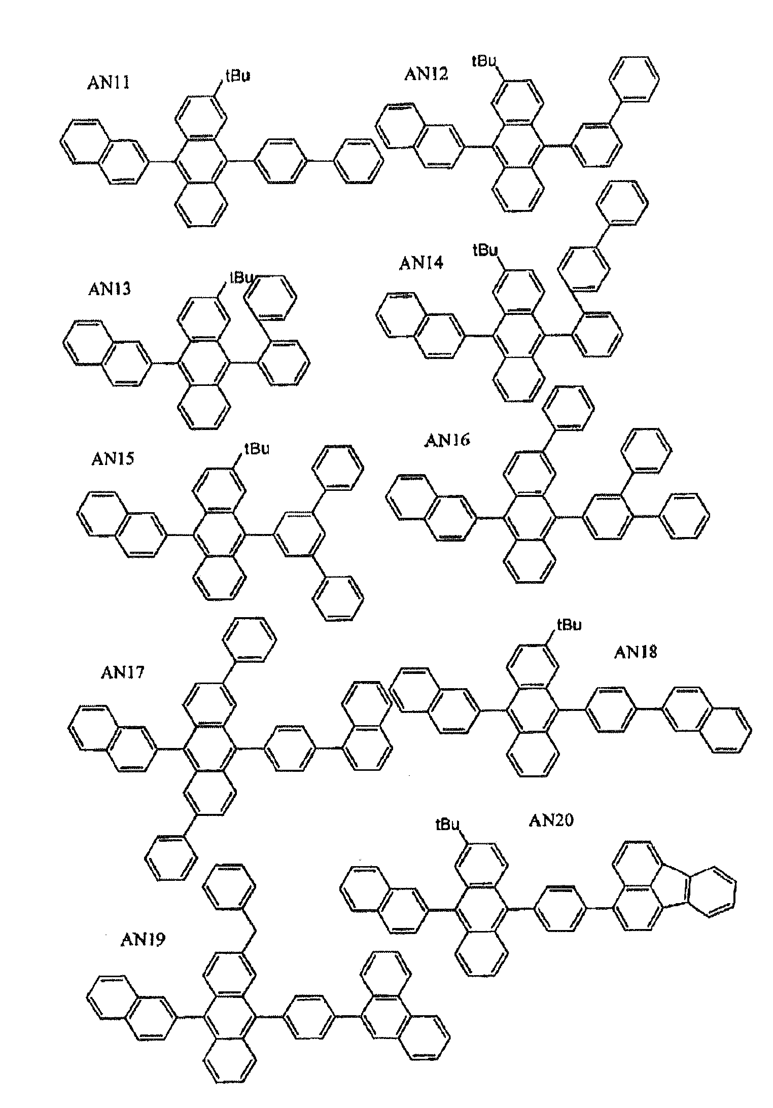
-


-


-


-


- The anthracene derivative may be an asymmetric monoanthracene derivative represented by a formula (3) as follows.
-

R1 to R10 are each a hydrogen atom, a substituted or unsubstituted aromatic ring group having 6 to 50 carbon atoms forming the aromatic ring, a substituted or unsubstituted aromatic heterocycle group having 5 to 50 atoms forming the aromatic ring, a substituted or unsubstituted alkyl group having 1 to 50 carbon atoms, a substituted or unsubstituted cycloalkyl group, a substituted or unsubstituted alkoxy group having 1 to 50 carbon atoms, a substituted or unsubstituted aralkyl group having 6 to 50 carbon atoms, a substituted or unsubstituted aryloxy group having 5 to 50 atoms forming the aromatic ring, a substituted or unsubstituted arylthio group having 5 to 50 atoms forming the aromatic ring, a substituted or unsubstituted alkoxycarbonyl group having 1 to 50 carbon atoms, substituted or unsubstituted silyl group, a carboxyl group, a halogen atom, a cyano group, a nitro group and a hydroxy group. - Examples of such an anthracene derivative are as follows.
-

Compound Ar1 Ar2 AN-1 1-naphthyl 9-phenanthryl AN-2 1-naphthyl 1-pyrenyl AN-3 1-naphthyl phenyl AN-4 1-naphthyl 2-biphenyl AN-5 1-naphthyl 3-biphenyl AN-6 1-naphthyl 4-biphenyl AN-7 1-naphthyl 2-p-ta-phenyl AN-8 2-naphthyl 1-naphthyl AN-9 2-naphthyl 9-phenanthryl AN-10 2-naphthyl 1-pyrenyl AN-11 2-naphthyl phenyl AN-12 2-naphthyl 2-biphenyl AN-13 2-naphthyl 3-biphenyl AN-14 2-naphthyl 4-biphenyl AN-15 2-naphthyl 2-p-ta-phenyl AN-16 9-phenanthryl 1-pyrenyl AN-17 9-phenanthryl phenyl AN-18 9-phenanthryl 2-biphenyl AN-19 9-phenanthryl 3-biphenyl AN-20 9-phenanthryl 4-biphenyl - [Formula 15]
AN-21 9-phenanthryl 2-p-ta-phenyl AN-22 1-biphenyl phenyl AN-23 1-biphenyl 2-biphenyl AN-24 1-biphenyl 3-biphenyl AN-25 1-biphenyl 4-biphenyl AN-26 1-biphenyl 2-p-ta-phenyl AN-27 phenyl 2-biphenyl AN-28 phenyl 3-biphenyl AN-29 phenyl 4-biphenyl AN-30 phenyl 2-p-ta-phenyl AN-31 2-biphenyl 3-biphenyl AN-32 2-biphenyl 4-biphenyl AN-33 2-biphenyl 2-p-ta-phenyl AN-34 3-biphenyl 4-biphenyl AN-35 3-biphenyl 2-p-ta-phenyl 
Compound Ar1 Ar2 AN-36 1-naphthyl 1-naphthyl AN-37 1-naphthyl 2-naphthyl AN-38 1-naphthyl 9-phenanthryl AN-39 1-naphthyl 1-pyrenyl - [Formula 16]
AN-40 1-naphthyl phenyl AN-41 1-naphthyl 2-biphenyl AN-42 1-naphthyl 3-biphenyl AN-43 1-naphthyl 4-biphenyl AN-44 1-naphthyl 2-p-ta-phenyl AN-45 2-naphthyl 1-naphthyl AN-46 2-naphthyl 2-naphthyl AN-47 2-naphthyl 9-phenanthryl AN-48 2-naphthyl 1-pyrenyl AN-49 2-naphthyl phenyl AN-50 2-naphthyl 2-biphenyl AN-51 2-naphthyl 3-biphenyl AN-52 2-naphthyl 4-biphenyl AN-53 2-naphthyl 2-p-ta-phenyl AN-54 9-phenanthryl 1-naphthyl AN-55 9-phenanthryl 2-naphthyl AN-56 9-phenanthryl 9-phenanthryl AN-57 9-phenanthryl 1-pyrenyl AN-58 9-phenanthryl phenyl AN-59 9-phenanthryl 2-biphenyl AN-60 9-phenanthryl 3-biphenyl AN-61 9-phenanthryl 4-biphenyl AN-62 9-phenanthryl 2-p-ta-phenyl AN-63 1-pyrenyl 1-naphthyl AN-64 1-pyrenyl 2-naphthyl - [Formula 17]
AN-65 1-pyrenyl 9-phenanthryl AN-66 1-pyrenyl 1-pyrenyl AN-67 1-pyrenyl phenyl AN-68 1-pyrenyl 2-biphenyl AN-69 1-pyrenyl 3-biphenyl AN-70 1-pyrenyl 4-biphenyl AN-71 1-pyrenyl 2-p-ta-phenyl AN-72 phenyl 1-naphthyl AN-73 phenyl 2-naphthyl AN-74 phenyl 9-phenanthryl AN-75 phenyl 1-pyrenyl AN-76 phenyl phenyl AN-77 phenyl 2-biphenyl AN-78 phenyl 3-biphenyl AN-79 phenyl 4-biphenyl AN-80 phenyl 2-p-ta-phenyl AN-81 2-biphenyl 1-naphthyl AN-82 2-biphenyl 2-naphthyl AN-83 2-biphenyl 9-phenanthryl AN-84 2-biphenyl 1-pyrenyl AN-85 2-biphenyl phenyl AN-86 2-biphenyl 2-biphenyl AN-87 2-biphenyl 3-biphenyl AN-88 2-biphenyl 4-biphenyl - [Formula 18]
AN-89 2-biphenyl 2-p-ta-phenyl AN-90 3-biphenyl 1-naphthyl AN-91 3-biphenyl 2-naphthyl AN-92 3-biphenyl 9-phenanthryl AN-93 3-biphenyl 1-pyrenyl AN-94 3-biphenyl phenyl AN-95 3-biphenyl 2-biphenyl AN-96 3-biphenyl 3-biphenyl AN-97 3-biphenyl 4-biphenyl AN-98 3-biphenyl 2-p-ta-phenyl AN-99 4-biphenyl 1-naphthyl AN-100 4-biphenyl 2-naphthyl AN-101 4-biphenyl 9-phenanthryl AN-102 4-biphenyl 1-pyrenyl AN-103 4-biphenyl phenyl AN-104 4-biphenyl 2-biphenyl AN-105 4-biphenyl 3-biphenyl AN-106 4-biphenyl 4-biphenyl AN-107 4-biphenyl 2-p-ta-phenyl -

Compound Ar1 Ar2 AN-108 1-naphthyl 1-naphthyl AN-109 1-naphthyl 2-naphthyl AN-110 1-naphthyl 9-phenanthryl AN-111 1-naphthyl 1-pyrenyl AN-112 1-naphthyl phenyl AN-113 1-naphthyl 2-biphenyl AN-114 1-naphthyl 3-biphenyl AN-115 1-naphthyl 4-biphenyl AN-116 1-naphthyl 2-p-ta-phenyl AN-117 2-naphthyl 1-naphthyl AN-118 2-naphthyl 2-naphthyl AN-119 2-naphthyl 9-phenanthryl AN-120 2-naphthyl 1-pyrenyl AN-121 2-naphthyl phenyl AN-122 2-naphthyl 2-biphenyl AN-123 2-naphthyl 3-biphenyl AN-124 2-naphthyl 4-biphenyl AN-125 2-naphthyl 2-p-ta-phenyl AN-126 9-phenanthryl 1-naphthyl AN-127 9-phenanthryl 2-naphthyl - [Formula 20]
AN-128 9-phenanthryl 9-phenanthryl AN-129 9-phenanthryl 1-pyrenyl AN-130 9-phenanthryl phenyl AN-131 9-phenanthryl 2-biphenyl AN-132 9-phenanthryl 3-biphenyl AN-133 9-phenanthryl 4-biphenyl AN-134 9-phenanthryl 2-p-ta-phenyl AN-13 5 1-pyrenyl 1-naphthyl AN-136 1-pyrenyl 2-naphthyl AN-13 7 1-pyrenyl 9-phenanthryl AN-138 1-pyrenyl 1-pyrenyl AN-139 1-pyrenyl phenyl AN-140 1-pyrenyl 2-biphenyl AN-141 1-pyrenyl 3-biphenyl AN-142 1-pyrenyl 4-biphenyl AN-143 1-pyrenyl 2-p-ta-phenyl AN-144 phenyl 1-naphthyl AN-145 phenyl 2-naphthyl AN-146 phenyl 9-phenanthryl AN-147 phenyl 1-pyrenyl AN-148 phenyl phenyl AN-149 phenyl 2-biphenyl AN-150 phenyl 3-biphenyl AN-151 phenyl 4-biphenyl AN-152 phenyl 2-p-ta-phenyl - [Formula 21]
AN-153 2-biphenyl 1-naphthyl AN-154 2-biphenyl 2-naphthyl AN-155 2-biphenyl 9-phenanthryl AN-156 2-biphenyl 1-pyrenyl AN-157 2-biphenyl phenyl AN-158 2-biphenyl 2-biphenyl AN-159 2-biphenyl 3-biphenyl AN-160 2-biphenyl 4-biphenyl AN-161 2-biphenyl 2-p-ta-phenyl AN-162 3-biphenyl 1-naphthyl AN-163 3-biphenyl 2-naphthyl AN-164 3-biphenyl 9-phenanthryl AN-165 3-biphenyl 1-pyrenyl AN-166 3-biphenyl phenyl AN-167 3-biphenyl 2-biphenyl AN-168 3-biphenyl 3-biphenyl AN-169 3-biphenyl 4-biphenyl AN-170 3-biphenyl 2-p-ta-phenyl AN-171 4-biphenyl 1-naphthyl AN-172 4-biphenyl 2-naphthyl AN-173 4-biphenyl 9-phenanthryl AN-174 4-biphenyl 1-pyrenyl AN-175 4-biphenyl phenyl AN-176 4-biphenyl 2-biphenyl - [Formula 22]
AN-177 4-biphenyl 3-biphenyl AN-178 4-biphenyl 4-biphenyl AN-179 4-biphenyl 2-p-ta-phenyl 
Compound Ar1 Ar2 AN-180 1-naphthyl 1-naphthyl AN-181 1-naphthyl 2-naphthyl AN-182 1-naphthyl 9-phenanthryl AN-183 1-naphthyl 1-pyrenyl AN-184 1-naphthyl phenyl AN-185 1-naphthyl 2-biphenyl AN-186 1-naphthyl 3-biphenyl AN-187 1-naphthyl 4-biphenyl AN-188 2-naphthyl 1-naphthyl AN-189 2-naphthyl 2-naphthyl AN-190 2-naphthyl 9-phenanthryl AN-191 2-naphthyl 1-pyrenyl AN-192 2-naphthyl phenyl AN-193 2-naphthyl 2-biphenyl AN-194 2-naphthyl 3-biphenyl AN-195 2-naphthyl 4-biphenyl - [Formula 23]
AN-196 9-phenanthryl 1-naphthyl AN-197 9-phenanthryl 2-naphthyl AN-198 9-phenanthryl 9-phenanthryl AN-199 9-phenanthryl 1-pyrenyl AN-200 9-phenanthryl phenyl AN-201 9-phenanthryl 2-biphenyl AN-202 9-phenanthryl 3-biphenyl AN-203 9-phenanthryl 4-biphenyl AN-204 1-pyrenyl 1-naphthyl AN-205 1-pyrenyl 2-naphthyl AN-206 1-pyrenyl 9-phenanthryl AN-207 1-pyrenyl 1-pyrenyl AN-208 1-pyrenyl phenyl AN-209 1-pyrenyl 2-biphenyl AN-210 1-pyrenyl 3-biphenyl AN-211 1-pyrenyl 4-biphenyl AN-212 phenyl 1-naphthyl AN-213 phenyl 2-naphthyl AN-214 phenyl 9-phenanthryl AN-215 phenyl 1-pyrenyl AN-216 phenyl phenyl AN-217 phenyl 2-biphenyl AN-218 phenyl 3-biphenyl AN-219 phenyl 4-biphenyl AN-220 2-biphenyl 1-naphthyl - [Formula 24]
AN-221 2-biphenyl 2-naphthyl AN-222 2-biphenyl 9-phenanthryl AN-223 2-biphenyl 1-pyrenyl AN-224 2-biphenyl phenyl AN-225 2-biphenyl 2-biphenyl AN-226 2-biphenyl 3-biphenyl AN-227 2-biphenyl 4-biphenyl AN-228 3-biphenyl 1-naphthyl AN-229 3-biphenyl 2-naphthyl AN-230 3-biphenyl 9-phenanthryl AN-231 3-biphenyl 1-pyrenyl AN-232 3-biphenyl phenyl AN-233 3-biphenyl 2-biphenyl AN-234 3-biphenyl 3-biphenyl AN-235 3-biphenyl 4-biphenyl AN-236 4-biphenyl 1-naphthyl AN-237 4-biphenyl 2-naphthyl AN-238 4-biphenyl 9-phenanthryl AN-239 4-biphenyl 1-pyrenyl AN-240 4-biphenyl phenyl AN-241 4-biphenyl 2-biphenyl AN-242 4-biphenyl 3-biphenyl AN-243 4-biphenyl 4-biphenyl -

Compound Ar1 Ar2 AN-244 1-naphthyl 2-naphthyl AN-245 1-naphthyl 9-phenanthryl AN-246 1-naphthyl 1-pyrenyl AN-247 1-naphthyl phenyl AN-248 1-naphthyl 2-biphenyl AN-249 1-naphthyl 3-biphenyl AN-250 1-naphthyl 4-biphenyl AN-251 2-naphthyl 9-phenanthryl AN-252 2-naphthyl 1-pyrenyl AN-253 2-naphthyl phenyl AN-254 2-naphthyl 2-biphenyl AN-255 2-naphthyl 3-biphenyl AN-256 2-naphthyl 4-biphenyl AN-257 9-phenanthryl 1-pyrenyl AN-258 9-phenanthryl phenyl AN-259 9-phenanthryl 2-biphenyl AN-260 9-phenanthryl 3-biphenyl AN-261 9-phenanthryl 4-biphenyl AN-262 1-pyrenyl phenyl AN-263 1-pyrenyl 2-biphenyl - [Formula 26]
AN-264 1-pyrenyl 3-biphenyl AN-265 1-pyrenyl 4-biphenyl AN-266 phenyl 2-biphenyl AN-267 phenyl 3-biphenyl AN-268 phenyl 4-biphenyl AN-269 2-biphenyl 3-biphenyl AN-270 2-biphenyl 4-biphenyl AN-271 3-biphenyl 4-biphenyl 
Compound Ar1 Ar2 AN-272 1-naphthyl 2-naphthyl AN-273 1-naphthyl 9-phenanthryl AN-274 1-naphthyl 1-pyrenyl AN-275 1-naphthyl phenyl AN-276 1-naphthyl 2-biphenyl AN-277 1-naphthyl 3-biphenyl AN-278 1-naphthyl 4-biphenyl AN-279 2-naphthyl 9-phenanthryl AN-280 2-naphthyl 1-pyrenyl AN-281 2-naphthyl phenyl AN-282 2-naphthyl 2-biphenyl - [Formula 27]
AN-283 2-naphthyl 3-biphenyl AN-284 2-naphthyl 4-biphenyl AN-285 9-phenanthryl 1-pyrenyl AN-286 9-phenanthryl phenyl AN-287 9-phenanthryl 2-biphenyl AN-288 9-phenanthryl 3-biphenyl AN-289 9-phenanthryl 4-biphenyl AN-290 1-pyrenyl phenyl AN-291 1-pyrenyl 2-biphenyl AN-292 1-pyrenyl 3-biphenyl AN-293 1-pyrenyl 4-biphenyl AN-294 phenyl 2-biphenyl AN-295 phenyl 3-biphenyl AN-296 phenyl 4-biphenyl AN-297 2-biphenyl 3-biphenyl AN-298 2-biphenyl 4-biphenyl AN-299 3-biphenyl 4-biphenyl 
Compound Ar1 Ar2 AN-300 1-naphthyl 1-naphthyl AN-301 1-naphthyl 2-naphthyl - [Formula 28]
AN-302 1-naphthyl 9-phenanthryl AN-303 1-naphthyl 1-pyrenyl AN-304 1-naphthyl phenyl AN-305 1-naphthyl 2-biphenyl AN-306 1-naphthyl 3-biphenyl AN-307 1-naphthyl 4-biphenyl AN-308 1-naphthyl 2-p-ta-phenyl AN-309 2-naphthyl 1-naphthyl AN-310 2-naphthyl 2-naphthyl AN-311 2-naphthyl 9-phenanthryl AN-312 2-naphthyl 1-pyrenyl AN-313 2-naphthyl phenyl AN-314 2-naphthyl 2-biphenyl AN-315 2-naphthyl 3-biphenyl AN-316 2-naphthyl 4-biphenyl AN-317 2-naphthyl 2-p-ta-phenyl 
Compound Ar1 Ar2 AN-318 1 -naphthyl 1-naphthyl AN-319 1-naphthyl 2-naphthyl AN-320 1-naphthyl 9-phenanthryl - [Formula 29]
AN-321 1-naphthyl 1-pyrenyl AN-322 1-naphthyl phenyl AN-323 1-naphthyl 2-biphenyl AN-324 1-naphthyl 3-biphenyl AN-325 1-naphthyl 4-biphenyl AN-326 1-naphthyl 2-p-ta-phenyl AN-327 2-naphthyl 1-naphthyl AN-328 2-naphthyl 2-naphthyl AN-329 2-naphthyl 9-phenanthryl AN-330 2-naphthyl 1-pyrenyl AN-331 2-naphthyl phenyl AN-332 2-naphthyl 2-biphenyl AN-333 2-naphthyl 3-biphenyl AN-334 2-naphthyl 4-biphenyl AN-335 2-naphthyl 2-p-ta-phenyl 
Compound Ar1 Ar2 AN-336 1-naphthyl 1-naphthyl AN-337 1-naphthyl 2-naphthyl AN-338 1-naphthyl 9-phenanthryl AN-339 1-naphthyl 1-pyrenyl - [Formula 30]
AN-340 1-naphthyl phenyl AN-341 1-naphthyl 2-biphenyl AN-342 1-naphthyl 3-biphenyl AN-343 1-naphthyl 4-biphenyl AN-344 1-naphthyl 2-p-ta-phenyl AN-345 2-naphthyl 1-naphthyl AN-346 2-naphthyl 2-naphthyl AN-347 2-naphthyl 9-phenanthryl AN-348 2-naphthyl 1-pyrenyl AN-349 2-naphthyl phenyl AN-350 2-naphthyl 2-biphenyl AN-351 2-naphthyl 3-biphenyl AN-352 2-naphthyl 4-biphenyl AN-353 2-naphthyl 2-p-ta-phenyl 
Compound Ar1 Ar2 AN-354 1-naphthyl 1-naphthyl AN-355 1-naphthyl 2-naphthyl AN-356 1-naphthyl 9-phenanthryl AN-357 1-naphthyl 1-pyrenyl AN-358 1-naphthyl phenyl - [Formula 31]
AN-359 1-naphthyl 2-biphenyl AN-360 1-naphthyl 3-biphenyl AN-361 1-naphthyl 4-biphenyl AN-362 1-naphthyl 2-p-ta-phenyl AN-363 2-naphthyl 1-naphthyl AN-364 2-naphthyl 2-naphthyl AN-365 2-naphthyl 9-phenanthryl AN-366 2-naphthyl 1-pyrenyl AN-367 2-naphthyl phenyl AN-368 2-naphthyl 2-biphenyl AN-369 2-naphthyl 3-biphenyl AN-370 2-naphthyl 4-biphenyl AN-371 2-naphthyl 2-p-ta-phenyl Compound Ar1 Ar2 AN-372 1-naphthyl 1-naphthyl AN-373 1-naphthyl 2-naphthyl AN-374 1-naphthyl 9-phenanthryl AN-375 1-naphthyl 1-pyrenyl AN-376 1-naphthyl phenyl AN-377 1-naphthyl 2-biphenyl - [Formula 32]
AN-378 1-naphthyl 3-biphenyl AN-379 1-naphthyl 4-biphenyl AN-380 1-naphthyl 2-p-ta-phenyl AN-3 81 2-naphthyl 1-naphthyl AN-382 2-naphthyl 2-naphthyl AN-383 2-naphthyl 9-phenanthryl AN-384 2-naphthyl 1-pyrenyl AN-385 2-naphthyl phenyl AN-386 2-naphthyl 2-biphenyl AN-387 2-naphthyl 3-biphenyl AN-388 2-naphthyl 4-biphenyl AN-389 2-naphthyl 2-p-ta-phenyl -


-


-


- The anthracene derivative may be a compound represented by a formula (4) as follows.
-


- In the above formula (4); at least either one of Ar1 and Ar2 is a substituent having a substituted or unsubstituted fused ring group with 10 to 30 carbon atoms forming the aromatic ring;
X1 and X2 are each a substituted or unsubstituted aromatic group having 6 to 50 carbon atoms forming the aromatic ring, a substituted or unsubstituted aromatic heterocycle group having 5 to 50 carbon atoms forming the aromatic ring, a substituted or unsubstituted alkyl group having 1 to 50 carbon atoms, a substituted or unsubstituted alkoxy group having 1 to 50 carbon atoms, a substituted or unsubstituted aralkyl group having 6 to 50 carbon atoms, a substituted or unsubstituted aryloxy group having 5 to 50 carbon atoms, a substituted or unsubstituted arylthio group having 5 to 50 carbon atoms, a substituted or unsubstituted alkoxycarbonyl group having 1 to 50 carbon atoms, a carboxyl group, a halogen group, a cyano group, a nitro group and hydroxyl group; and
a and b are each an integer in a range of 0 to 4, a plurality of X1 being mutually the same or different when a is 2 or more, a plurality of X2 being mutually the same or different when b is 2 or more. - Examples of a substituent group of Ar1 and Ar2 in the formula (4), the substituent group including a fused ring group with 10 to 30 carbon atoms forming the aromatic ring, are a substituted or unsubstituted α-naphthyl group, a substituted or unsubstituted β-naphthyl group, a substituted or unsubstituted phenanthryl group, a substituted or unsubstituted crycenyl group, a substituted or unsubstituted tetracenyl group, a substituted or unsubstited pyrenyl group, a substituted or unsubstituted phenylnaphthyl group, a substituted or unsubstituted naphthylnaphthyl group, a substituted or unsubstituted naphthylphenyl group, a substituted or unsubstituted phenylpyrenyl group, a substituted or unsubstituted pyrenylphenyl group, a substituted or unsubstituted naphthylnaphthylnaphthyl group, a substituted or unsubstituted naphthylnaphthylphenyl group, a substituted or unsubstituted naphthylphenylnaphthyl group, a substituted or unsubstituted phenylnaphthylnaphthyl group, a substituted or unsubstituted phenylnaphthylphenyl group, a substituted or unsubstituted phenylphenylnaphthyl group.
A preferable group among the above is a substituted or unsubstituted α-naphthyl group, a substituted or unsubstituted β-naphthyl group, a substituted or unsubstituted phenylnaphthyl group, a substituted or unsubstituted naphthylnaphthyl group or a substituted or unsubstituted naphthylphenyl group. - Examples of such an anthracene derivative are as follows.
-


-


-


- Examples of a dopant used together with the host containing the above anthracene derivative are a styrylamine derivative represented by a formula (5) as follows and a substituted derivative of arylamine represented by a formula (6) as follows.
-


- The aromatic group having 6 to 20 carbon atoms is preferably a phenyl group, a naphthyl group, an anthracenyl group, a phenanthryl group, a terphenyl group or the like.
-

- In the formula above, the aryl group having 5 to 40 ring atoms is preferably phenyl, naphthyl, anthracenyl, phenanthryl, pyrenyl, chrysenyl, coronyl, biphenyl, terphenyl, pyrrolyl, furanyl, thiophenyl, benzothiophenyl, oxadiazolyl, diphenyl anthracenyl, indolyl, carbazolyl, pyridyl, benzoquinolyl, fluorenyl, fluoranthenyl, acenaphthofluoranthenyl, stilbene, a group represented by a general formula (A) or (B) below or the like.
In the general formula (A), r is an integer in a range of 1 to 3. -

- The aryl group having 5 to 40 ring atoms may be substituted by a substituent group, in which the substituent group is preferably an alkyl group having 2 to 6 carbon atoms (e.g., an ethyl group, a methyl group, an isopropyl group, an n-propyl group, an s-butyl group, a t-butyl group, a pentyl group, a hexyl group, a cyclopentyl group and a cyclohexyl group).
- Examples of the dopant are compounds shown below.
-


-


-


-


-


-


-


-


-


-


-

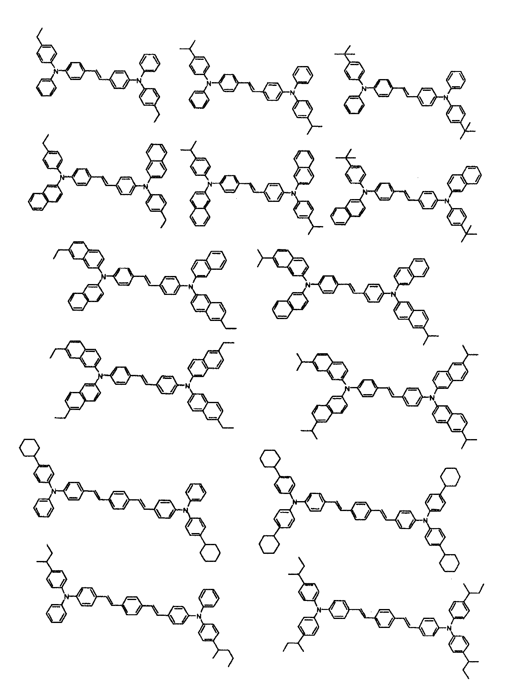
- The hole injecting/transporting layer(s) helps injection of the holes into the emitting layer and transports the holes to an emitting region. In the hole injecting/transporting layer(s), the hole mobility is large while the energy of ionization is typically small (5.5 eV or smaller). A material of the hole injecting/transporting layer(s) is preferably such a material that transports the holes to the emitting layer with a lower field intensity, and more preferably such a material that transports the holes with the hole mobility of at least 10-4 cm2/Vs when the exemplary electrical field of 104 to 106 V/cm is applied.
- In the organic electroluminescence device according to the present embodiment, the hole injecting layer contains poly(alkylene dioxythiophene) and at least one fluorine-containing colloid-forming polymer acid.
The poly(alkylene dioxythiophene) is poly(3,4-dioxythiophene).
The fluorine-containing colloid-forming polymer acid is a fluorine-containing polymer sulfonic acid, a fluorine-containing polymer carboxylic acid, a fluorine-containing polymer phosphoric acid, a fluorine-containing polymer acrylic acid or a mixture of the above.
The fluorine-containing colloid-forming polymer acid is preferably a perfluorinated polymer acid. - A colloid-forming polymer acid usable in implementing the present invention is insoluble in water. When dispersed in an aqueous medium, the colloid-forming polymer acid forms a colloid. A molecular weight of a polymer acid is typically in a range of approximately 10,000 to approximately 4,000,000. In one embodiment, the molecular weight of a polymer acid is in a range of approximately 100,000 to approximately 2,000,000. A diameter of a colloid particle is typically in a range of 2 nanometer (nm) to approximately 140 nm. In one embodiment, the diameter of a colloid particle is in a range of 2 nm to approximately 30 nm. Any polymer acid may be preferably used in implementing the present invention as long as the polymer acid forms a colloid when dispersed in water. In one embodiment, the colloid-forming polymer acid is a polymer sulfonic acid. Examples of another usable polymer acid are a polymer phosphoric acid, a polymer carboxylic acid and a polymer acrylic acid. Mixtures of the above polymer acids, an example of which is a mixture containing a polymer sulfonic acid, are also usable. In another embodiment, the colloid-forming polymer sulfonic acid is perfluorinated. In a still further embodiment, the colloid-forming polymer sulfonic acid is a perfluoro alkylene sulfonic acid.
- In a still further embodiment, the colloid-forming polymer acid is a highly-fluorinated sulfonate polymer (FSA polymer). "highly-fluorinated" means that: at least approximately 50% of the total halogens and hydrogen atoms contained in the polymer are substituted by fluorine atoms; at least approximately 75% thereof are substituted by fluorine atoms in one embodiment; and at least approximately 90% thereof are substituted by fluorine atoms in another embodiment. In one embodiment, the polymer is perfluorinated. A term "sulfonate functional group" herein means either one of a sulfonate group and a salt of a sulfonate group. In one embodiment, the term means either one of an alkali metal and an ammonium salt. The functional group is represented by a formula of -SO3X (where X represents a cation, which is also known as "counterion"). X may be H, Li, Na, K or N(R1)(R2)(R3)(R4), in which R1, R2, R3 and R4 may be the same or different from one another. In one embodiment, R1, R2, R3 and R4 are H, CH3 or C2H5. In another embodiment, X is H. In such an embodiment, the polymer is said to be in an "acid form". In addition, X may be multivalent as represented by an ion such as Ca++ and Al+++. When a multivalent counterion as generally represented by Mn+ is concerned, a person skilled in the art will clearly understand that the number of sulfonate functional group(s) per counterion is equal to the valence number "n" of the counterion.
- In one embodiment, the FSA polymer contains a polymer main chain in which a repeated side chain(s) having a cation-exchange group is bonded to a main chain. The polymer may be a homopolymer or a copolymer of plural monomers. The copolymer is typically formed from a non-functionalized monomer and a second monomer having a cation-exchange group or its precursor such as a sulfonyl fluoride group (-SO2F) that can be subsequently hydrolyzed to sulfonate functional group. For instance, a copolymer of a first fluorinated vinyl monomer and a second fluorinated vinyl monomer having a sulfonyl fluoride group (-SO2F) may be used as the copolymer. Examples of a monomer usable as the first monomer are tetrafluoroethylene (TFE), hexafluoropropylene, fluorinated vinyl, fluorinated vinylidene, trifluoroethylene, chlorotrifluoroethylene, perfluoro(alkyl vinyl ether) and a combination of the above monomers. The first monomer is preferably TFE.
- In another embodiment, a monomer usable as the second monomer may be fluorinated vinyl ether having a sulfonate functional group or a precursor group capable of providing a desirable side chain(s) to the polymer. An additional monomer such as ethylene, propylene and R-CH=CH2 (where R is a perfluorinated alkyl group having 1 to 10 carbon atoms) may be added into the above polymers as necessary. The polymer may be a copolymer that is herein called a random copolymer, i.e., a copolymer manufactured by polymerization where a relative concentration of the comonomer is kept as constant as possible so that a distribution of monomer units along the polymer chain consequently corresponds to relative concentrations and relative reactivity of the monomer units. A less random copolymer manufactured by changing the relative concentrations of monomers during polymerization is also usable. Such a polymer as disclosed in Patent Document 2, which is called a block copolymer, is also usable.
- According to one embodiment, the FSA polymer to be used in the present invention contains a highly-fluorinated carbon main chain and side chain(s) represented by a formula as follows while the carbon main chain may be perfluorinated in another embodiment:
-(O-CF2CFRf)a-O-CF2CFR'fSO3X
(In the formula: Rf and R'f are each selected from a group consisting of F, Cl and a perfluorinated alkyl group having 1 to 10 carbon atoms; "a" is any one of 0, 1 and 2; and X is any one of H, Li, Na, K and N(R1(R2)(R3)(R4), in which the R1, R2, R3 and R4 may be mutually the same or different, the R1, R2, R3 and R4 being H, CH3 or C2H5 in one embodiment). In another embodiment, the X is H. As described above, the X may also be multivalent. - In one embodiment, the FSA polymer contains such a polymer as disclosed in
US Patent No. 3,282,875 ,US Patent No. 4,358,545 andUS Patent No. 4,940,525 . A preferable example of the FSA polymer contains a perfluorocarbon main chain and a side chain(s) represented by a formula as follows:
-O-CF2CF(CF3)-O-CF2CF2SO3X
(where X is defined as above). The above type of the FSA polymer, which is disclosed inUS Patent No. 3,282,875 , can be manufactured by: copolymerizing tetrafluoroethylene (TFE) and perfluorinated vinyl ether CF2=CF-O-CF2CF(CF3)-O-CF2CF2SO2F (perfluoro(3,6-dioxa-4-methyl-7-octene sulfonyl fluoride)) (PDMOF); subsequently converting the sulfonyl fluoride group into a sulfonate group by hydrolysis; and converting the above into desirable ion form by ion exchange as necessary. Such a polymer as disclosed inUS Patent No. 4,358,545 andUS Patent No. 4,940,525 contains side chain(s) represented by -O-CF2CF2SO3X where X is defined as above. Such a polymer can be manufactured by: copolymerizing tetrafluoroethylene (TFE) and perfluorinated vinyl ether CF2=CF-O-CF2CF2SO2F (perfluoro(3-oxa-4-pentene sulfonyl fluoride)) (POPF); subsequently hydrolyzing the above; and further performing ion exchange as necessary. - In one embodiment, the FSA polymer to be used in the present invention typically has an ion-exchange ratio of less than approximately 33. The "ion-exchange ratio" or "IXR" herein is defined as the number of carbon atoms included in a polymer main chains in relation to a cation-exchange group. IXR may be changed within a range of less than approximately 33 to be suitable for a specific use. IXR is in a range of approximately 3 to 33 in one embodiment while in a range of approximately 8 to 23 in another embodiment.
- Cation-exchange capacity of the polymer is frequently represented in equivalent weight (EW). The equivalent weight (EW) herein is defined as a weight of a polymer in an acid form required for neutralizing 1 equivalent weight of sodium hydrate. When a polymer is a sulfonate polymer that has a perfluorocarbon main chain and side chain(s) of -O-CF2-CF(CF3)-O-CF2-CF2-SO3H (or a salt thereof), the IXR in the range of approximately 8 to 23 corresponds to an equivalent-weight range of approximately 750 to 1500 EW. The IXR of this polymer can be related to the equivalent weight by using a formula of 50 IXR + 344 = EW. Although the same IXR range may be used for, for instance, polymer(s) containing the side chain(s) of -O-CF2CF2SO3H (or a salt thereof) among the sulfonate polymers disclosed in
US Patent No. 4,358,545 andUS Patent No. 4,940,525 , the equivalent weights thereof are lowered by some degree due to lower molecular weights of monomer units containing cation-exchange groups. The preferable IXR range of approximately 8 to 23 corresponds to an equivalent-weight range of approximately 575 to 1325 EW. The IXR of this polymer can be related to the equivalent weight by using a formula of 50 + IXR 178 = EW. - The FSA polymer may be manufactured as a colloidal aqueous dispersion solution. The polymer may be a dispersion solution using another medium. Such medium are exemplarily water-soluble ether such as alcohol and tetrahydrofuran, a mixture of water-soluble ether and combinations thereof but are not limited to the above. In manufacturing a dispersion solution, the polymer may be used in acid form.
US Patent No. 4,433,082 ,US Patent No. 6,150,426 and International Publication No.03/006537 - An aqueous dispersion solution of a colloid-forming polymer acid such as the FSA polymer typically forms colloid of as small particle diameter as possible and has as small EW as possible, as long as stable colloid is formed.
- An aqueous dispersion solution of the FSA polymer is commercially available as Nafion (Registered Trademark) dispersion solution from E.I. du Pont de Nemours and Company (Wilmington, DE).
- The electron injecting/transporting layer may further be laminated between the organic emitting layer and the cathode. The electron injecting/transporting layer, which helps injection of the electron into the emitting layer, has a high electron mobility.
In the organic electroluminescence device, since emitted light is reflected by an electrode (the cathode, in this case), light directly provided through the anode and the light provided after being reflected by the electrode are known to interfere with each other. In order to efficiently utilize the interference, the thickness of the electron transporting layer is suitably selected from the range of several nanometers to several micrometers. However, especially when the thickness of the layer is large, the electron mobility is preferably at least 10-5 cm2/Vs or higher so as to prevent voltage rise when the electrical field of 104 to 106 V/cm is applied . - In the organic electroluminescence device according to the present embodiment, the electron transporting layer contains a compound having electron mobility of 1 x 10⁻⁴ to 1 x 10⁻² cm2/Vs at an electric field intensity of 2.5 x 10⁵V/cm. Particularly, the electron transporting layer preferably contains a nitrogen-containing heterocycle derivative represented by the following formula (1).
HAr-L-Ar1-Ar2 (1)
In the above formula (1): HAr represents a substituted or unsubstituted nitrogen-containing heterocycle group having 3 to 40 carbon atoms;
L represents a single bond, a substituted or unsubstituted arylene group having 6 to 60 carbon atoms, a substituted or unsubstituted heteroarylene group having 3 to 60 carbon atoms, or a substituted or unsubstituted fluorenylene group;
Ar1 represents a substituted or unsubstituted divalent aromatic hydrocarbon group having 6 to 60 carbon atoms; and
Ar2 represents a substituted or unsubstituted aryl group having 3 to 60 carbon atoms.
Examples of such a nitrogen-containing heterocycle derivative are shown below. However, the present invention is not limited to exemplification as follows. -

-

-


-


-


-

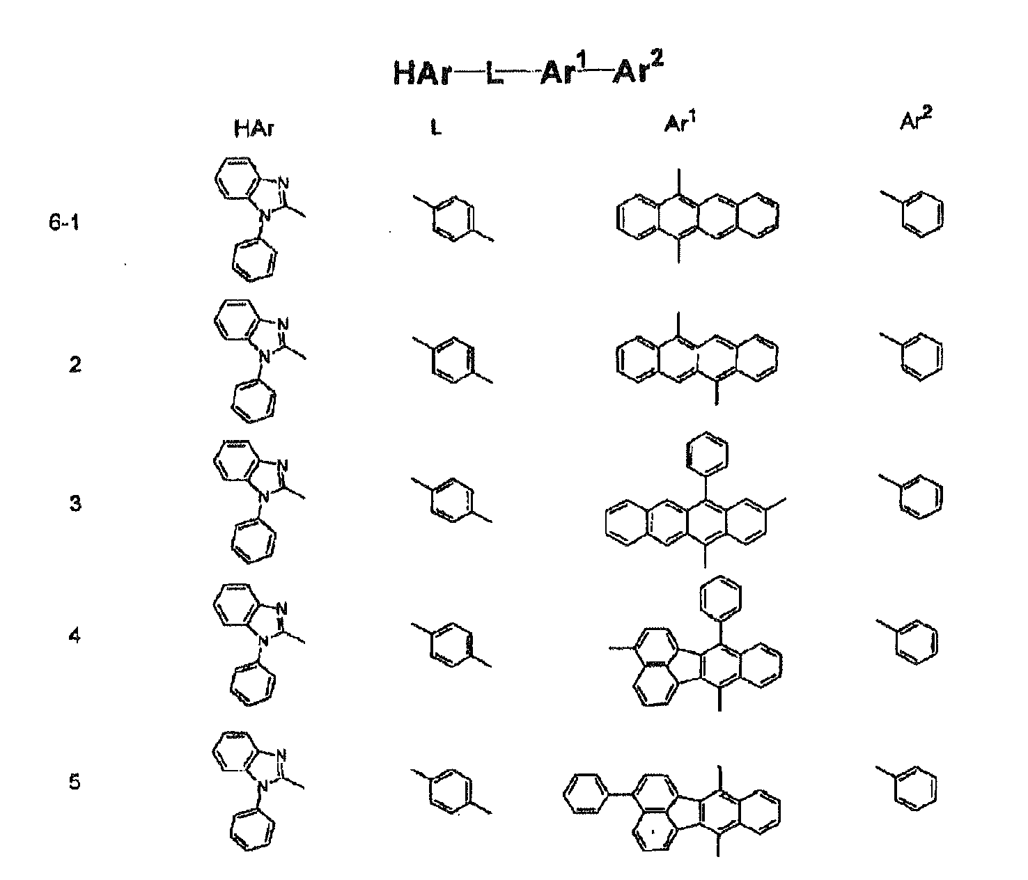
-

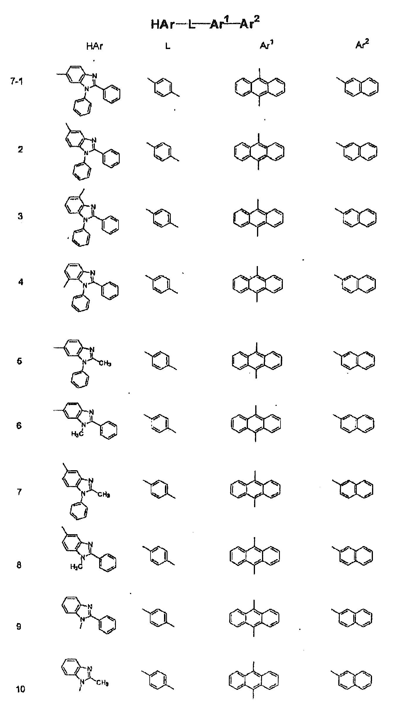
-


-


-


-


-


-


-


-


-


-


- As a preferred embodiment of the organic electroluminescence device, there is known a device containing a reductive dopant at a boundary between a region transporting the electron or the cathode and an organic layer. Here, the reductive dopant is defined as a substance capable of reducing an electron transporting compound. Thus, various substances having a certain level of reducibility can be used, preferable examples of which are at least one substance selected from a group consisting of: alkali metal, an oxide of the alkali metal, a halogenide of the alkali metal, an organic complex of the alkali metal, alkali earth metal, an oxide of the alkali earth metal, a halogenide of the alkali earth metal, an organic complex of the alkali earth metal, rare earth metal, an oxide of the rare earth metal, a halogenide of the rare earth metal and an organic complex of the rare earth metal.
- Specifically, reductive dopant is preferably a substance(s) having the work function of 2.9 eV or lower, which is exemplified by at least one alkali metal selected from a group consisting of Li (work function: 2.9 eV), Na (work function: 2.36 eV), K (work function: 2.28 eV), Rb (work function: 2.16 eV) and Cs (work function: 1.95 eV) or at least one alkali earth metal selected from a group consisting of Ca (work function: 2.9 eV), Sr (work function: 2 to 2.5 eV) and Ba (work function: 2.52 eV), and the substances having the work function of 2.9 eV or lower are particularly preferable. Among these, more preferable reductive dopant is at least one alkali metal selected from a group consisting of K, Rb and Cs, in which Rb and Cs are even more preferable and Cs is the most preferable. These alkali metals have particularly high reducibility, so that addition of a relatively small amount of these alkali metals to an electron injecting zone can enhance luminescence intensity and lifecycle of the organic electroluminescence device. In addition, as the reductive dopant having the work function of 2.9 eV or lower, a combination of two or more of these alkali metals is also preferable, and a combination including Cs is particularly preferable (e.g. combinations of Cs and Na, Cs and K, Cs and Rb or Cs, Na and K). The combinations including Cs can effectively exert the reducibility, so that the addition of such reductive dopant to the electron injecting zone can enhance the luminescence intensity and the lifecycle of the organic electroluminescence device.
- An electron injecting layer formed from an insulator or a semiconductor may be provided between the cathode and the organic layer. With the arrangement, leak of electric current can be effectively prevented and the electron injecting capability can be enhanced. As the insulator, it is preferable to use at least one metal compound selected from a group consisting of an alkali metal chalcogenide, an alkali earth metal chalcogenide, a halogenide of alkali metal and a halogenide of alkali earth metal. By forming the electron injecting layer from the alkali metal chalcogenide or the like, the electron injecting capability can preferably be further enhanced. Specifically, preferable examples of the alkali metal chalcogenide are Li2O, K2O, Na2S, Na2Se and Na2O, while preferable example of the alkali earth metal chalcogenide are CaO, BaO, SrO, BeO, BaS and CaSe. Preferable examples of the halogenide of the alkali metal are LiF, NaF, KF, LiCl, KCl and NaCl. Preferable examples of the halogenide of the alkali earth metal are fluorides such as CaF2, BaF2, SrF2, MgF2 and BeF2, and halogenides other than the fluoride.
Examples of the semiconductor for forming the electron transporting layer are one of or a combination of two or more of an oxide, a nitride or an oxidized nitride containing at least one element selected from a group consisting of Ba, Ca, Sr, Yb, Al, Ga, In, Li, Na, Cd, Mg, Si, Ta, Sb and Zn. An inorganic compound for forming the electron transporting layer is preferably a microcrystalline or amorphous semiconductor film. When the electron transporting layer is formed of such semiconductor film, more uniform thin film can be formed, thereby reducing pixel defects such as a dark spot. Examples of such an inorganic compound are the above-described alkali metal chalcogenide, alkali earth metal chalcogenide, halogenide of the alkali metal and halogenide of the alkali earth metal. - In order to inject the electrons into the electron inj ecting/transporting layer or the emitting layer, a material whose work function is small (4 eV or lower) is used as an electrode material for the cathode, examples of the material being metals, alloys, electrically conductive compounds and mixtures thereof. Examples of the electrode material are sodium, a sodium-potassium alloy, magnesium, lithium, a magnesium-silver alloy, aluminium/aluminium oxide, an aluminium-lithium alloy, indium, rare earth metal and the like.
The cathode may be made by forming a thin film from the electrode material by vapor deposition and sputtering.
When luminescence from the emitting layer is provided through the cathode, the cathode preferably transmits more than 10% of the luminescence.
The sheet resistance as the cathode is preferably several hundreds Ω/ square or lower, and the thickness of the film is typically in a range from 10 nm to 1 µm, preferably 50 to 200 nm. - Since the electrical field is applied to ultra thin films in the organic electroluminescence device, pixel defects resulted from leak or short circuit are likely to occur. In order to prevent such defects, it is preferable to interpose an insulating thin film layer between a pair of electrodes.
Examples of a material used for the insulating layer are aluminum oxide, lithium fluoride, lithium oxide, cesium fluoride, cesium oxide, magnesium oxide, magnesium fluoride, calcium oxide, calcium fluoride, aluminium nitride, titanium oxide, silicon oxide, germanium oxide, silicon nitride, boron nitride, molybdenum oxide, ruthenium oxide, vanadium oxide and the like.
Mixtures or laminates thereof may also be used. - The organic electroluminescence device can be manufactured by forming the anode, the emitting layer, the hole injecting layer (as necessary), the electron injecting layer (as necessary) and the cathode form the materials listed above by the above-described formation methods. The organic electroluminescence device can also be manufactured by forming the above elements in the inverse order of the above, namely from the cathode to the anode.
- The following is an example of a manufacturing method of the organic electroluminescence device in which the anode, the hole injecting layer, the emitting layer, the electron injecting layer and the cathode are sequentially formed on the light-transmissive substrate.
- A thin film is formed of the anode material on a suitable light-transmissive substrate by vapor deposition or sputtering such that the thickness of the thin film is 1 µm or smaller, preferably in a range from 10 nm to 200 nm, thereby forming the anode.
Then, the hole injecting layer is formed on the formed anode.
The hole injecting layer can be formed by vacuum deposition, spin coating, casting method, LB method or the like. The thickness of the hole injecting layer is suitably determined within a range of 5 nm to 5 µm. - Then, the emitting layer is formed on the hole injecting layer by forming a thin film from an organic luminescent material by a dry process represented by the vacuum deposition or a wet process such as spin coating and casting method.
- Then, the electron injecting layer is formed on the emitting layer.
The electron injecting layer may be exemplarily formed by vacuum deposition. - Lastly, the cathode is laminated on the electron injecting layer, whereby the organic electroluminescence device can be obtained.
The cathode can be formed from a metal by a method such as vapor deposition and sputtering.
In order to protect the organic layers deposited under the cathode from being damaged, the vacuum deposition is preferable. - The methods for forming each of the layers in the organic electroluminescence device are not particularly limited.
Conventional methods such as vacuum deposition and spin coating can be employed for forming the organic film layers. Specifically, the organic film layers may be formed by a conventional coating method such as vacuum deposition, molecular beam epitaxy (MBE method) and coating methods using a solution such as a dipping, spin coating, casting, bar coating, roll coating and ink jet printing.
Although the thickness of each organic layer of the organic electroluminescence device is not particularly limited, the thickness is generally preferably in a range of several nanometers to 1 µm because excessively-thinned film likely entails defects such as a pin hole while excessively-thickened film requires high voltage to be applied and deteriorates efficiency.
When a direct current is applied to the organic electroluminescence device, the luminescence can be observed by applying a voltage of 5 to 40V with the anode having the positive polarity and the cathode having the negative polarity. When the voltage is applied with the inversed polarity, no current flows, so that the luminescence is not generated. When an alternating current is applied, the uniform luminescence can be observed only when the anode has the positive polarity and the cathode has the negative polarity. A waveform of the alternating current to be applied may be suitably selected. - Example(s) of the present invention will be described.
- Electron mobility was measured with a time-of-flight measuring machine TOF-401 manufactured by Sumitomo Heavy Industries Advanced Machinery.
Using a translucent metal electrode (Al: 10nm) as the anode while using a transparent oxide electrode (ITO: 130nm) as the cathode, a sample was laminated on the machine by 3 µm so as to measure the mobility. The ITO substrate used as the cathode was cleaned in the same manner as in later-described Example 1. In addition, each material was laminated by vapor deposition as in Example 1.
The sample was set on a sample chamber of the time-of-flight measuring machine TOF-401, and the sample was connected to the anode and the cathode both by a gold-coated probe. Signal current was detected by observing terminal voltages of parallely-connected load resistors with an oscilloscope. - Observation of the signal current is conducted simultaneously with irradiation of laser beam. The current is decreased after some time has lapsed. The decrease in the current means that a sheet of electrons has reached the anode. The inflection time (movement time) is represented by tT.
Electron mobility µe is defined as in a following formula.
In the formula, "d" represents a film thickness of the sample while E represents an electric field intensity.
In general, the electron mobility depends on the electric field intensity. When the mobility is plotted with the square root of the electric field intensity, a linear shape is frequently observed. Accordingly, when the mobility is defined as a numeric value, conditions of the electric field intensity should be specified when the mobility is measured. A value when the electric field intensity was 2.5 x 10⁵ (V/cm) was used as the value of the mobility (cm2/Vs) herein. - 40g of a poly(3,4-ethylenedioxithiophene)/ polystyrene sulfonate solution with a concentration of 1.32% (manufactured by H.C. StarckGmbH, product name: Baytron™ P, TPAI4083, in which a mass ratio of PEDOT to PSS was 1: 6) was mixed with 9.96g of a solution prepared by dissolving Nafion™ in a mixture of lower aliphatic alcohol and water with a concentration of 5.30 mass% (a solution in which Nafion™ perfluorinated ion-exchange resin was dissolved in a mixture of lower aliphatic alcohol/H2O with a concentration of 5 mass%, CAS-No. 66796-30-3, Aldrich order No. 27,470-4, a verified solid content of 5.30 mass%). The mass ratio between PEDOT, PSS and Nafion™ was 1: 6: 7.
- A glass substrate (size: 25 mm x 75 mm x 1.1 mm thick) having an ITO transparent electrode (manufactured by Geomatics) was ultrasonic-cleaned in isopropyl alcohol for five minutes, and then UV/ozone-cleaned for 30 minutes.
A mixture of PEDOT and Nafion™ prepared as described above was applied on the substrate by spin coating to form a film of 50 nm. The layer serves as the hole injecting layer.
N,N,N',N'-tetra(4-biphenyl)-diamine biphenylene (hereinafter called, "TBDB layer") was deposited on the layer by vacuum deposition to form a film of 20nm. The layer serves as the hole transporting layer.
Then, the compounds AN-1 and BD-1 (mass ratio of AN-1 to BD-1 was 20: 1) were simultaneously deposited thereon to form an emitting layer of 40nm thickness.
An electron transporting material (ET-1, electron mobility: 1.1 x 10⁻⁴ cm2/Vs, hereinafter abbreviated as "ET film") was deposited on the film to form a film of 20nm thickness. The ET film serves as the electron transporting layer.
Subsequently, LiF was deposited thereon to form a film of 1nm thickness, such that 150nm thick Al was deposited on the LiF film to form a metal cathode, thereby providing an organic electroluminescence device. Luminous efficiency, voltage and chromaticity at 10mA/cm2 of the obtained organic electroluminescence device were measured. In addition, a room temperature when the initial luminescence intensity was 5000cd/m2 and time elapsed until a half-life of the luminescence intensity when the device was driven by DC constant current were measured. -


- In place of the mixture of PEDOT and Nafion™ described in the above Example 1, copper phthalocyanine (CuPc) was deposited to form a film of 100nm, and in place of the electron transporting material (ET), an aluminum quinolinol complex (Alq3, electron mobility: 5 x 10⁻⁶ cm2/Vs) was deposited to form a film of 20nm.
- In place of the electron transporting material (ET-1) described in the above Example 1, an aluminum quinolinol complex (Alq3) was deposited to form a film of 20nm.
- In place of the mixture of PEDOT and Nafion™ described in the above Example 1, copper phthalocyanine (CuPc) was deposited to form a film of 50nm.
- In place of the mixture of PEDOT and Nafion™ described in the above Example 1, PEDOT-PSS was deposited to form a film of 50nm.
- In place of the compounds AN-1 and BD-1 described in the above Example 1, compounds RH and RD as follows (weight ratio of RH: RD = 40: 0.4) were deposited to form an emitting layer of 40nm thickness.
-

- In place of the mixture of REDOT and Nafion™ described in the above Example 1, PEDOT-PSS was deposited to form a film of 50nm, and in place of the compounds AN-1 and BD-1, the compounds RH and RD (weight ratio of RH: RD = 40: 0.4) were deposited to form an emitting layer of 40nm thickness.
Evaluation results of the Example 1 and Comparatives 1 to 6 are shown in Table 1. -
[Table 1] Hole Injecting Layer Emitting Layer Electron Transporting Layer Voltage Efficiency Chromaticity Lifetime (V) (cd/A) (x,y) (h) Example 1 PEDOT:PSS: Nafion™ AN-1:BD-1 ET1 5.5 6.0 (0.14, 0.18) 500 Comparative 1 CuPc AN-1: BD-1 Alq 8.0 4.4 (0.14, 0.17) 300 Comparative 2 PEDOT:PSS: Nafion™ AN-1:BD-1 Alq 6.5 4.8 (0.14, 0.20) 300 Comparative 3 CuPc AN-1: BD-1 ET1 6.0 4.9 (0.14, 0.17) 100 Comparative 4 PEDOT:PSS AN-1: BD-1 ET1 5.9 4.6 (0.14, 0.18) 350 Comparative 5 PEDOT:PSS: Nafion™ RH:RD Alq 4.9 7.4 (0.65, 0.35) Comparative 6 PEDOT:PSS RH:RD Alq 5.1 6.9 (0.64, 0.35) - As is understood from Table 1, the blue-emitting organic electroluminescence device of Example 1 is much more excellent in driving voltage, luminous efficiency, chromatic purity and lifetime than the blue-emitting organic electroluminescence devices of Comparatives 1 to 4 arranged in the same manner as a conventional device.
In contrast, although the organic electroluminescence device of Comparative 1 exhibits the chromaticity of almost the same level as that of Example 1, the driving voltage required by Comparative 1 is high because its hole injecting layer is CuPc. In addition, since its electron transporting layer is made of an Alq complex whose electron mobility is low, Comparative 1 is inferior in luminous efficiency and lifetime. - The organic electroluminescence device of Comparative 2 requires lower driving voltage than that of Comparative 1 because its hole injecting layer uses the mixture of PEDOT and Nafion™ as in Example 1. However, since its electron transporting layer is an Alq complex whose electron mobility is low, the emitting region in the emitting layer is shifted toward the cathode. Thus, the value of chromaticity y-coordinate of Comparative 2 is large, and luminous efficiency and lifetime of Comparative 2 are inferior.
The organic electroluminescence device of Comparative 3 requires a lower driving voltage than that of Comparative 1 because its electron transporting layer is formed of ET1. However, since its hole injecting layer is CuPc, Comparative 3 exhibits much shorter lifetime. - In the organic electroluminescence device of Comparative 4, the hole injecting layer only contains the mixture of PEDOT and PSS and does not contain Nafion™, Nafion™, which is a perfluorinated polymer, contains a lot of fluorine. Thus, a hole injecting layer containing Nafion™ exhibits lower refractivity. Example 1, where the hole injecting layer containing Nafion™ was used, employs a structure of a high reflectivity layer (emitting layer + hole transporting layer) / a low reflectivity layer (hole injecting layer) / a high reflectivity layer (ITO), thereby increasing optical interference modes and enhancing light-extraction efficiency of blue-emitting wavelength. As a consequence, luminous efficiency is enhanced. On the other hand, Comparative 4, where the hole injecting layer does not contain Nafion™, hardly produces the above effects, thereby exhibiting lower luminous efficiency.
- Comparatives 5 and 6 show a difference between the hole injecting layers with and without Nafion™ in a red-emitting organic electroluminescence device. Compared as the luminous efficiency of Comparative 6 that does not contain Nafion™, Comparative 5 containing Nafion™ exhibits merely slightly-improved luminous efficiency. Materials used for the emitting layer and the hole transporting layer (i.e., low-molecular material), which generally exhibits high reflectivity in a blue short-wavelength region, exhibits lower and lower reflectivity as the wavelength becomes longer than the blue region. The transparent conductive material used for anode exhibits a similar tendency. On the other hand, reflectivity of polymer materials for hole injecting used in Example 1 and Comparatives 2 to 6 is less dependant on the wavelength. Accordingly, a reflectivity difference between the emitting layer, the hole transporting layer and ITO and the hole injecting layer in the red-emitting wavelength region is smaller than the reflectivity difference in the blue-emitting wavelength region, such that the light-extraction efficiency is less improved. Thus, the presence of Nafion™ is less effective on such a red-emitting device.
- This invention can be used as an organic electroluminescence device containing mixed color for a display.
Claims (11)
- An organic electroluminescence device, comprising an anode, a hole injecting layer, an emitting layer, an electron transporting layer and a cathode in this order, wherein
the hole injecting layer comprises: substituted or unsubstituted poly(alkylene dioxythiophene); and a fluorine-containing colloid-forming polymer acid, and
the electron transporting layer comprises a compound having electron mobility of 1.0 x 10⁻⁴cm2/Vs or more at an electric field intensity of 2.5 x 10⁵V/cm. - The organic electroluminescence device according to Claim 1, wherein the electron transporting layer comprises a nitrogen-containing heterocycle derivative represented by a formula (1) as follows,
HAr-L-Ar1Ar2 (1)
(where: HAr represents a substituted or unsubstituted nitrogen-containing heterocycle group having 3 to 40 carbon atoms;
L represents a single bond, a substituted or unsubstituted arylene group having 6 to 60 carbon atoms, a substituted or unsubstituted heteroarylene group having 3 to 60 carbon atoms, or a substituted or unsubstituted fluorenylene group;
Ar1 represents a substituted or unsubstituted divalent aromatic hydrocarbon group having 6 to 60 carbon atoms; and
Ar2 represents a substituted or unsubstituted aryl group having 3 to 60 carbon atoms.) - The organic electroluminescence device according to Claim 1 or 2, wherein
the emitting layer comprises a host and a dopant, and
the host is formed of a material having a molecular weight of 4000 or less. - The organic electroluminescence device according to Claim 3, wherein the host comprises a fused-ring compound having at least three rings.
- The organic electroluminescence device according to Claim 4, wherein the fused-ring compound having at least three rings is an anthracene derivative.
- The organic electroluminescence device according to Claim 5, wherein the anthracene derivative is represented by a formula (2) as follows,

Ar' represents a substituted or unsubstituted aromatic group having 6 to 50 carbon atoms forming the aromatic ring;
X1 to X3 each represent a substituted or unsubstituted aromatic group having 6 to 50 carbon atoms forming the aromatic ring, a substituted or unsubstituted aromatic heterocyclic group having 5 to 50, a substituted or unsubstituted alkyl group having 1 to 50 carbon atoms, a substituted or unsubstituted alkoxy group having 1 to 50 carbon atoms, a substituted or unsubstituted aralkyl group having 6 to 50 carbon atoms, a substituted or unsubstituted aryloxy group having 5 to 50 carbon atoms, a substituted or unsubstituted arylthio group having 5 to 50 carbon atoms, a substituted or unsubstituted alkoxycarbonyl group having 1 to 50 carbon atoms, a carboxyl group, a halogen group, a cyano group, a nitro group and a hydroxyl group;
a, b and c are each an integer in a range of 0 to 4, a plurality of X1 being mutually the same or different when a is 2 or more, a plurality of X2 being mutually the same or different when b is 2 or more, a plurality of X3 being mutually the same or different when c is 2 or more; and
n is an integer in a range of 1 to 3 while m is 0 or 1, a plurality of such structures shown in the brackets [ ] as represented by a formula below being mutually the same or different when n is 2 or more.)
- The organic electroluminescence device according to Claim 5, wherein the anthracene derivative is an asymmetric monoanthracene derivative represented by a formula (3) as follows,

R1 to R10 are each a hydrogen atom, a substituted or unsubstituted aromatic ring group having 6 to 50 carbon atoms forming the aromatic ring, a substituted or unsubstituted aromatic heterocycle group having 5 to 50 atoms forming the aromatic ring, a substituted or unsubstituted alkyl group having 1 to 50 carbon atoms, a substituted or unsubstituted cycloalkyl group, a substituted or unsubstituted alkoxy group having 1 to 50 carbon atoms, a substituted or unsubstituted aralkyl group having 6 to 50 carbon atoms, a substituted or unsubstituted aryloxy group having 5 to 50 atoms forming the aromatic ring, a substituted or unsubstituted arylthio group having 5 to 50 atoms forming the aromatic ring, a substituted or unsubstituted alkoxycarbonyl group having 1 to 50 carbon atoms, substituted or unsubstituted silyl group, a carboxyl group, a halogen atom, a cyano group, a nitro group and a hydroxy group.) - The organic electroluminescence device according to Claim 5, wherein the anthracene derivative is represented by a formula (4) as follows,

X1 and X2 are each a substituted or unsubstituted aromatic group having 6 to 50 carbon atoms forming the aromatic ring, a substituted or unsubstituted aromatic heterocycle group having 5 to 50, a substituted or unsubstituted alkyl group having 1 to 50 carbon atoms, a substituted or unsubstituted alkoxy group having 1 to 50 carbon atoms, a substituted or unsubstituted aralkyl group having 6 to 50 carbon atoms, a substituted or unsubstituted aryloxy group having 5 to 50 carbon atoms, a substituted or unsubstituted arylthio group having 5 to 50 carbon atoms, a substituted or unsubstituted alkoxycarbonyl group having 1 to 50 carbon atoms, a carboxyl group, a halogen group, a cyano group, a nitro group and hydroxyl group; and
a and b are each an integer in a range of 0 to 4, a plurality of X1 being mutually the same or different when a is 2 or more, a plurality of X2 being mutually the same or different when b is 2 or more.) - The organic electroluminescence device according to any one of Claims 1 to 8, wherein the substituted or unsubstituted poly(alkylene dioxythiophene) is poly(3,4-ethylenedioxithiophene).
- The organic electroluminescence device according to any one of Claims 1 to 9, wherein the fluorine-containing colloid-forming polymer acid is selected from a group consisting of a fluorine-containing polymer sulfonic acid, a fluorine-containing polymer carboxylic acid, a fluorine-containing polymer phosphoric acid, a fluorine-containing polymer acrylic acid and a mixture of the acids.
- The organic electroluminescence device according to any one of Claims 1 to 10, wherein the fluorine-containing colloid-forming polymer acid is a perfluorinated polymer sulfonic acid.
Applications Claiming Priority (2)
| Application Number | Priority Date | Filing Date | Title |
|---|---|---|---|
| JP2007050857 | 2007-02-28 | ||
| PCT/JP2008/052873 WO2008105294A1 (en) | 2007-02-28 | 2008-02-20 | Organic el device |
Publications (2)
| Publication Number | Publication Date |
|---|---|
| EP2124270A1 true EP2124270A1 (en) | 2009-11-25 |
| EP2124270A4 EP2124270A4 (en) | 2010-08-25 |
Family
ID=39721129
Family Applications (1)
| Application Number | Title | Priority Date | Filing Date |
|---|---|---|---|
| EP08711679A Withdrawn EP2124270A4 (en) | 2007-02-28 | 2008-02-20 | ORGANIC ELECTROLUMINESCENCE DEVICE |
Country Status (6)
| Country | Link |
|---|---|
| US (1) | US20090167156A1 (en) |
| EP (1) | EP2124270A4 (en) |
| JP (1) | JPWO2008105294A1 (en) |
| KR (1) | KR20090128427A (en) |
| TW (1) | TW200848489A (en) |
| WO (1) | WO2008105294A1 (en) |
Cited By (2)
| Publication number | Priority date | Publication date | Assignee | Title |
|---|---|---|---|---|
| EP3104428A1 (en) * | 2009-06-12 | 2016-12-14 | Idemitsu Kosan Co., Ltd | Organic electroluminescence device |
| US10950805B2 (en) | 2017-05-19 | 2021-03-16 | Semiconductor Energy Laboratory Co., Ltd. | Electronic device, light-emitting device, electronic appliance, and lighting device |
Families Citing this family (31)
| Publication number | Priority date | Publication date | Assignee | Title |
|---|---|---|---|---|
| US20100295445A1 (en) * | 2009-05-22 | 2010-11-25 | Idemitsu Kosan Co., Ltd. | Organic electroluminescent device |
| US9153790B2 (en) * | 2009-05-22 | 2015-10-06 | Idemitsu Kosan Co., Ltd. | Organic electroluminescent device |
| DE102009041289A1 (en) * | 2009-09-16 | 2011-03-17 | Merck Patent Gmbh | Organic electroluminescent device |
| DE102009053191A1 (en) * | 2009-11-06 | 2011-05-12 | Merck Patent Gmbh | Materials for electronic devices |
| TW201229003A (en) * | 2010-12-17 | 2012-07-16 | Du Pont | Anthracene derivative compounds for electronic applications |
| WO2012083301A1 (en) * | 2010-12-17 | 2012-06-21 | E. I. Du Pont De Nemours And Company | Anthracene derivative compounds for electronic applications |
| KR101831015B1 (en) | 2011-01-20 | 2018-02-21 | 이데미쓰 고산 가부시키가이샤 | Organic electroluminescent element |
| TWI644463B (en) * | 2012-10-26 | 2018-12-11 | 黑拉耶烏斯貴金屬公司 | Transparent layer with high conductivity and high performance in OLEDs and manufacturing method thereof |
| KR102002025B1 (en) * | 2012-12-24 | 2019-07-19 | 에스에프씨주식회사 | Antracene derivatives having heteroaryl substituted naphthyl group and organic light-emitting diode including the same |
| KR101492527B1 (en) * | 2013-01-25 | 2015-02-12 | 에스에프씨 주식회사 | Organic light-emitting diode including aryl substituted antracene derivatives |
| JP6142213B2 (en) | 2013-07-11 | 2017-06-07 | 株式会社Joled | ORGANIC EL ELEMENT AND METHOD FOR PRODUCING ORGANIC EL ELEMENT |
| JP6286943B2 (en) * | 2013-08-28 | 2018-03-07 | セイコーエプソン株式会社 | LIGHT EMITTING DEVICE AND ELECTRONIC DEVICE |
| JP6359256B2 (en) * | 2013-09-25 | 2018-07-18 | 出光興産株式会社 | ORGANIC ELECTROLUMINESCENT ELEMENT AND ELECTRONIC DEVICE |
| JP6548359B2 (en) * | 2014-05-12 | 2019-07-24 | キヤノン株式会社 | Organic light emitting device |
| WO2017043731A1 (en) * | 2015-09-07 | 2017-03-16 | 엘지전자 주식회사 | Method for cancelling self-interference by apparatus that uses fdr scheme |
| KR102563713B1 (en) | 2017-04-26 | 2023-08-07 | 오티아이 루미오닉스 인크. | Methods of patterning the coating of a surface and apparatus comprising the patterned coating |
| CN117715451A (en) | 2017-09-12 | 2024-03-15 | 株式会社半导体能源研究所 | Light-emitting element, light-emitting device, electronic apparatus, and lighting device |
| JP2019114780A (en) * | 2017-12-22 | 2019-07-11 | 株式会社半導体エネルギー研究所 | Electronic device, light emitting device, light emitting apparatus, electronic device, and lighting device |
| US11751415B2 (en) | 2018-02-02 | 2023-09-05 | Oti Lumionics Inc. | Materials for forming a nucleation-inhibiting coating and devices incorporating same |
| KR102866258B1 (en) | 2018-05-17 | 2025-09-29 | 가부시키가이샤 한도오따이 에네루기 켄큐쇼 | Organic compounds, light-emitting elements, light-emitting devices, electronic devices, lighting devices, and electronic devices |
| KR20250079071A (en) | 2018-06-06 | 2025-06-04 | 가부시키가이샤 한도오따이 에네루기 켄큐쇼 | Light emitting device, display device, and electronic device |
| CN113302181A (en) | 2018-11-16 | 2021-08-24 | 株式会社半导体能源研究所 | Organic compound, EL device, light-emitting device, electronic apparatus, lighting device, and electronic device |
| CN113412438A (en) | 2019-02-06 | 2021-09-17 | 株式会社半导体能源研究所 | Light-emitting device, light-emitting apparatus, electronic apparatus, display apparatus, and lighting apparatus |
| KR20250160226A (en) | 2019-03-07 | 2025-11-11 | 오티아이 루미오닉스 인크. | Materials for forming a nucleation-inhibiting coating and devices incorporating same |
| US11903232B2 (en) | 2019-03-07 | 2024-02-13 | Semiconductor Energy Laboratory Co., Ltd. | Light-emitting device comprising charge-generation layer between light-emitting units |
| KR102919127B1 (en) | 2019-03-07 | 2026-01-29 | 가부시키가이샤 한도오따이 에네루기 켄큐쇼 | luminescent device |
| JP7555600B2 (en) | 2019-04-18 | 2024-09-25 | オーティーアイ ルミオニクス インコーポレーテッド | Materials for forming nucleation-inhibiting coatings and devices incorporating same - Patents.com |
| JP7576337B2 (en) | 2019-05-08 | 2024-11-01 | オーティーアイ ルミオニクス インコーポレーテッド | Materials for forming nucleation-inhibiting coatings and devices incorporating same - Patents.com |
| JP7609606B2 (en) | 2019-11-08 | 2025-01-07 | 株式会社半導体エネルギー研究所 | Light-emitting device, electronic device and lighting device |
| US12113279B2 (en) | 2020-09-22 | 2024-10-08 | Oti Lumionics Inc. | Device incorporating an IR signal transmissive region |
| US11985841B2 (en) | 2020-12-07 | 2024-05-14 | Oti Lumionics Inc. | Patterning a conductive deposited layer using a nucleation inhibiting coating and an underlying metallic coating |
Family Cites Families (41)
| Publication number | Priority date | Publication date | Assignee | Title |
|---|---|---|---|---|
| BE566401A (en) | 1957-04-10 | 1900-01-01 | ||
| US3282875A (en) | 1964-07-22 | 1966-11-01 | Du Pont | Fluorocarbon vinyl ether polymers |
| US4358545A (en) | 1980-06-11 | 1982-11-09 | The Dow Chemical Company | Sulfonic acid electrolytic cell having flourinated polymer membrane with hydration product less than 22,000 |
| US4356429A (en) * | 1980-07-17 | 1982-10-26 | Eastman Kodak Company | Organic electroluminescent cell |
| US4433082A (en) | 1981-05-01 | 1984-02-21 | E. I. Du Pont De Nemours And Company | Process for making liquid composition of perfluorinated ion exchange polymer, and product thereof |
| US4940525A (en) | 1987-05-08 | 1990-07-10 | The Dow Chemical Company | Low equivalent weight sulfonic fluoropolymers |
| JP3228502B2 (en) * | 1996-10-08 | 2001-11-12 | 出光興産株式会社 | Organic electroluminescence device |
| EP0932646B1 (en) | 1996-10-15 | 2001-07-25 | E.I. Du Pont De Nemours And Company | Compositions containing particles of highly fluorinated ion exchange polymer |
| JP3525034B2 (en) * | 1997-07-31 | 2004-05-10 | 出光興産株式会社 | Organic electroluminescence device |
| TW521537B (en) * | 1998-05-08 | 2003-02-21 | Idemitsu Kosan Co | Organic electroluminescence element |
| DE19841803A1 (en) | 1998-09-12 | 2000-03-16 | Bayer Ag | Organic electroluminescent device, i.e. light-emitting diode, has hole-injecting layer of polymeric organic conductor formed by coating from solution or from sub-micron dispersion |
| US6465115B2 (en) * | 1998-12-09 | 2002-10-15 | Eastman Kodak Company | Electroluminescent device with anthracene derivatives hole transport layer |
| JP4040249B2 (en) * | 2000-11-16 | 2008-01-30 | 富士フイルム株式会社 | Light emitting element |
| KR100424090B1 (en) | 2001-06-25 | 2004-03-22 | 삼성에스디아이 주식회사 | A hole transport layer for electroluminescent device, an electrroluminescent device using the same, and the method thereof |
| US6986963B2 (en) * | 2001-12-14 | 2006-01-17 | Ut-Battelle Llc | Metallization of bacterial cellulose for electrical and electronic device manufacture |
| JP4363050B2 (en) | 2002-01-31 | 2009-11-11 | 住友化学株式会社 | Organic electroluminescence device |
| JP2003229277A (en) * | 2002-02-04 | 2003-08-15 | Matsushita Electric Ind Co Ltd | Light emitting device material, light emitting device and device using the same |
| JP4646494B2 (en) * | 2002-04-11 | 2011-03-09 | 出光興産株式会社 | Novel nitrogen-containing heterocyclic derivative and organic electroluminescence device using the same |
| WO2004018587A1 (en) * | 2002-08-23 | 2004-03-04 | Idemitsu Kosan Co., Ltd. | Organic electroluminescence device and anthracene derivative |
| DE60322923D1 (en) | 2002-09-24 | 2008-09-25 | Du Pont | WATER DISPERSIBLE POLYTHIOPHENE MANUFACTURES |
| AU2003279014A1 (en) | 2002-09-24 | 2004-04-19 | E.I. Du Pont De Nemours And Company | Water dispersible polyanilines made with polymeric acid colloids for electronics applications |
| KR101020350B1 (en) | 2003-03-13 | 2011-03-08 | 이데미쓰 고산 가부시키가이샤 | Novel nitrogen-containing heterocyclic derivatives and organic electroluminescent devices using the same |
| US7056601B2 (en) * | 2003-10-24 | 2006-06-06 | Eastman Kodak Company | OLED device with asymmetric host |
| KR101156241B1 (en) * | 2003-12-01 | 2012-06-13 | 이데미쓰 고산 가부시키가이샤 | Asymmetric monoanthracene derivative, material for organic electroluminescent device and organic electroluminescent device utilizing the same |
| US20050175861A1 (en) | 2004-02-10 | 2005-08-11 | H.C. Starck Gmbh | Polythiophene compositions for improving organic light-emitting diodes |
| DE102004006583A1 (en) * | 2004-02-10 | 2005-09-01 | H.C. Starck Gmbh | Polythiophene formulations for improving organic light-emitting diodes |
| KR20060135801A (en) * | 2004-03-05 | 2006-12-29 | 이데미쓰 고산 가부시키가이샤 | Organic electroluminescent element and organic electroluminescent display |
| WO2005091684A1 (en) * | 2004-03-19 | 2005-09-29 | Idemitsu Kosan Co., Ltd. | Organic electroluminescent device |
| JP4621201B2 (en) * | 2004-03-25 | 2011-01-26 | 出光興産株式会社 | Organic electroluminescence device |
| KR101110890B1 (en) * | 2004-04-02 | 2012-03-13 | 이데미쓰 고산 가부시키가이샤 | Organic electroluminescence element having two electroluminescent layers through electron barrier layer |
| WO2006046441A1 (en) * | 2004-10-29 | 2006-05-04 | Idemitsu Kosan Co., Ltd. | Aromatic amine compound and organic electroluminescent device using same |
| WO2006070712A1 (en) * | 2004-12-28 | 2006-07-06 | Idemitsu Kosan Co., Ltd. | Luminescent ink composition for organic electroluminescent device |
| US7670506B1 (en) * | 2004-12-30 | 2010-03-02 | E. I. Du Pont De Nemours And Company | Photoactive compositions for liquid deposition |
| CN101094828A (en) * | 2005-01-05 | 2007-12-26 | 出光兴产株式会社 | Aromatic amine derivative and organic electroluminescent device using same |
| JP2006190759A (en) * | 2005-01-05 | 2006-07-20 | Idemitsu Kosan Co Ltd | Organic electroluminescence device |
| WO2006103848A1 (en) * | 2005-03-25 | 2006-10-05 | Idemitsu Kosan Co., Ltd. | Aromatic amine derivative and organic electroluminescent element employing the same |
| KR100696505B1 (en) * | 2005-03-31 | 2007-03-19 | 삼성에스디아이 주식회사 | Organic electroluminescent device and manufacturing method thereof |
| JP5317386B2 (en) * | 2005-08-05 | 2013-10-16 | 出光興産株式会社 | Nitrogen-containing heterocyclic derivative and organic electroluminescence device using the same |
| US9666826B2 (en) * | 2005-11-30 | 2017-05-30 | Global Oled Technology Llc | Electroluminescent device including an anthracene derivative |
| US20070252517A1 (en) * | 2006-04-27 | 2007-11-01 | Eastman Kodak Company | Electroluminescent device including an anthracene derivative |
| JP2008166629A (en) * | 2006-12-29 | 2008-07-17 | Idemitsu Kosan Co Ltd | Organic EL material-containing solution, organic EL material synthesis method, compound synthesized by this synthesis method, organic EL material thin film formation method, organic EL material thin film, organic EL element |
-
2008
- 2008-02-20 JP JP2009501199A patent/JPWO2008105294A1/en active Pending
- 2008-02-20 KR KR1020097020002A patent/KR20090128427A/en not_active Withdrawn
- 2008-02-20 EP EP08711679A patent/EP2124270A4/en not_active Withdrawn
- 2008-02-20 WO PCT/JP2008/052873 patent/WO2008105294A1/en not_active Ceased
- 2008-02-26 TW TW097106644A patent/TW200848489A/en unknown
- 2008-02-26 US US12/037,511 patent/US20090167156A1/en not_active Abandoned
Cited By (3)
| Publication number | Priority date | Publication date | Assignee | Title |
|---|---|---|---|---|
| EP3104428A1 (en) * | 2009-06-12 | 2016-12-14 | Idemitsu Kosan Co., Ltd | Organic electroluminescence device |
| US10950805B2 (en) | 2017-05-19 | 2021-03-16 | Semiconductor Energy Laboratory Co., Ltd. | Electronic device, light-emitting device, electronic appliance, and lighting device |
| US12022725B2 (en) | 2017-05-19 | 2024-06-25 | Semiconductor Energy Laboratory Co., Ltd. | Electronic device, light-emitting device, electronic appliance, and lighting device |
Also Published As
| Publication number | Publication date |
|---|---|
| WO2008105294A1 (en) | 2008-09-04 |
| US20090167156A1 (en) | 2009-07-02 |
| EP2124270A4 (en) | 2010-08-25 |
| TW200848489A (en) | 2008-12-16 |
| KR20090128427A (en) | 2009-12-15 |
| JPWO2008105294A1 (en) | 2010-06-03 |
Similar Documents
| Publication | Publication Date | Title |
|---|---|---|
| US20090167156A1 (en) | Organic electroluminescence device | |
| TWI500196B (en) | Organic light emitting device and method of producing the same | |
| JP5324217B2 (en) | Conductive polymer composition | |
| TWI495707B (en) | The organic light emitting diode and manufacturing method thereof | |
| KR101422864B1 (en) | Organic electroluminescent device using heterocyclic-containing arylamine derivative | |
| CN101595532B (en) | Buffer compositions | |
| JP4915650B2 (en) | Organic electroluminescence device | |
| JP4915913B2 (en) | Organic electroluminescence device | |
| US20150137100A1 (en) | Organic Electroluminescent Device | |
| TW200305630A (en) | Organic light emitting diode devices with improved operational stability | |
| JP2010534739A (en) | Aqueous dispersion of conductive polymer containing inorganic nanoparticles | |
| JP2002038140A (en) | Organic luminescent layer and electroluminescent device | |
| KR20080080383A (en) | Organic light emitting device | |
| EP1755362B1 (en) | Organic el device | |
| JP2014169418A (en) | Ink for charge transport membrane, aromatic oligo iodonium salt usable to charge transport membrane, and method for producing charge transport membrane using the ink for charge transport membrane | |
| IL166738A (en) | Polythiophene formulations for improving organic light-emitting diodes | |
| TW201030085A (en) | Electrically conductive polymer compositions | |
| JP5211043B2 (en) | Manufacturing method of organic light emitting diode | |
| US20040146744A1 (en) | Material for an electroluminescence element and electroluminescence element using the same | |
| JP2010092940A (en) | Organic electroluminescent element | |
| CN101351851A (en) | Cationic compositions of electrically conducting polymers doped with fully-fluorination acid polymerization | |
| KR101314912B1 (en) | Electroluminescent materials and devices | |
| US20070018568A1 (en) | Organic electroluminescent device | |
| JP2000106277A (en) | Organic electroluminescent device | |
| KR101258701B1 (en) | Organic electroluminescent polymer having arylamine unit containing 9'-aryl-fluoren-9'-yl group and organic electroluminescent device manufactured using the same |
Legal Events
| Date | Code | Title | Description |
|---|---|---|---|
| PUAI | Public reference made under article 153(3) epc to a published international application that has entered the european phase |
Free format text: ORIGINAL CODE: 0009012 |
|
| 17P | Request for examination filed |
Effective date: 20090916 |
|
| AK | Designated contracting states |
Kind code of ref document: A1 Designated state(s): AT BE BG CH CY CZ DE DK EE ES FI FR GB GR HR HU IE IS IT LI LT LU LV MC MT NL NO PL PT RO SE SI SK TR |
|
| DAX | Request for extension of the european patent (deleted) | ||
| A4 | Supplementary search report drawn up and despatched |
Effective date: 20100726 |
|
| RIC1 | Information provided on ipc code assigned before grant |
Ipc: H01L 51/50 20060101AFI20080915BHEP Ipc: H05B 33/14 20060101ALI20100720BHEP |
|
| STAA | Information on the status of an ep patent application or granted ep patent |
Free format text: STATUS: THE APPLICATION HAS BEEN WITHDRAWN |
|
| 18W | Application withdrawn |
Effective date: 20100830 |