EP2124263B1 - Reflection type optical sensor device - Google Patents
Reflection type optical sensor device Download PDFInfo
- Publication number
- EP2124263B1 EP2124263B1 EP09160742.4A EP09160742A EP2124263B1 EP 2124263 B1 EP2124263 B1 EP 2124263B1 EP 09160742 A EP09160742 A EP 09160742A EP 2124263 B1 EP2124263 B1 EP 2124263B1
- Authority
- EP
- European Patent Office
- Prior art keywords
- light source
- optical sensor
- sensor device
- reflection type
- type optical
- Prior art date
- Legal status (The legal status is an assumption and is not a legal conclusion. Google has not performed a legal analysis and makes no representation as to the accuracy of the status listed.)
- Not-in-force
Links
Images


Classifications
-
- H—ELECTRICITY
- H10—SEMICONDUCTOR DEVICES; ELECTRIC SOLID-STATE DEVICES NOT OTHERWISE PROVIDED FOR
- H10H—INORGANIC LIGHT-EMITTING SEMICONDUCTOR DEVICES HAVING POTENTIAL BARRIERS
- H10H29/00—Integrated devices, or assemblies of multiple devices, comprising at least one light-emitting semiconductor element covered by group H10H20/00
- H10H29/10—Integrated devices comprising at least one light-emitting semiconductor component covered by group H10H20/00
-
- H—ELECTRICITY
- H10—SEMICONDUCTOR DEVICES; ELECTRIC SOLID-STATE DEVICES NOT OTHERWISE PROVIDED FOR
- H10F—INORGANIC SEMICONDUCTOR DEVICES SENSITIVE TO INFRARED RADIATION, LIGHT, ELECTROMAGNETIC RADIATION OF SHORTER WAVELENGTH OR CORPUSCULAR RADIATION
- H10F55/00—Radiation-sensitive semiconductor devices covered by groups H10F10/00, H10F19/00 or H10F30/00 being structurally associated with electric light sources and electrically or optically coupled thereto
- H10F55/20—Radiation-sensitive semiconductor devices covered by groups H10F10/00, H10F19/00 or H10F30/00 being structurally associated with electric light sources and electrically or optically coupled thereto wherein the electric light source controls the radiation-sensitive semiconductor devices, e.g. optocouplers
- H10F55/25—Radiation-sensitive semiconductor devices covered by groups H10F10/00, H10F19/00 or H10F30/00 being structurally associated with electric light sources and electrically or optically coupled thereto wherein the electric light source controls the radiation-sensitive semiconductor devices, e.g. optocouplers wherein the radiation-sensitive devices and the electric light source are all semiconductor devices
- H10F55/255—Radiation-sensitive semiconductor devices covered by groups H10F10/00, H10F19/00 or H10F30/00 being structurally associated with electric light sources and electrically or optically coupled thereto wherein the electric light source controls the radiation-sensitive semiconductor devices, e.g. optocouplers wherein the radiation-sensitive devices and the electric light source are all semiconductor devices formed in, or on, a common substrate
-
- H—ELECTRICITY
- H10—SEMICONDUCTOR DEVICES; ELECTRIC SOLID-STATE DEVICES NOT OTHERWISE PROVIDED FOR
- H10F—INORGANIC SEMICONDUCTOR DEVICES SENSITIVE TO INFRARED RADIATION, LIGHT, ELECTROMAGNETIC RADIATION OF SHORTER WAVELENGTH OR CORPUSCULAR RADIATION
- H10F77/00—Constructional details of devices covered by this subclass
- H10F77/40—Optical elements or arrangements
- H10F77/413—Optical elements or arrangements directly associated or integrated with the devices, e.g. back reflectors
-
- H—ELECTRICITY
- H01—ELECTRIC ELEMENTS
- H01S—DEVICES USING THE PROCESS OF LIGHT AMPLIFICATION BY STIMULATED EMISSION OF RADIATION [LASER] TO AMPLIFY OR GENERATE LIGHT; DEVICES USING STIMULATED EMISSION OF ELECTROMAGNETIC RADIATION IN WAVE RANGES OTHER THAN OPTICAL
- H01S5/00—Semiconductor lasers
- H01S5/005—Optical components external to the laser cavity, specially adapted therefor, e.g. for homogenisation or merging of the beams or for manipulating laser pulses, e.g. pulse shaping
-
- H—ELECTRICITY
- H01—ELECTRIC ELEMENTS
- H01S—DEVICES USING THE PROCESS OF LIGHT AMPLIFICATION BY STIMULATED EMISSION OF RADIATION [LASER] TO AMPLIFY OR GENERATE LIGHT; DEVICES USING STIMULATED EMISSION OF ELECTROMAGNETIC RADIATION IN WAVE RANGES OTHER THAN OPTICAL
- H01S5/00—Semiconductor lasers
- H01S5/02—Structural details or components not essential to laser action
- H01S5/026—Monolithically integrated components, e.g. waveguides, monitoring photo-detectors, drivers
- H01S5/0262—Photo-diodes, e.g. transceiver devices, bidirectional devices
-
- H—ELECTRICITY
- H01—ELECTRIC ELEMENTS
- H01S—DEVICES USING THE PROCESS OF LIGHT AMPLIFICATION BY STIMULATED EMISSION OF RADIATION [LASER] TO AMPLIFY OR GENERATE LIGHT; DEVICES USING STIMULATED EMISSION OF ELECTROMAGNETIC RADIATION IN WAVE RANGES OTHER THAN OPTICAL
- H01S5/00—Semiconductor lasers
- H01S5/10—Construction or shape of the optical resonator, e.g. extended or external cavity, coupled cavities, bent-guide, varying width, thickness or composition of the active region
- H01S5/18—Surface-emitting [SE] lasers, e.g. having both horizontal and vertical cavities
- H01S5/183—Surface-emitting [SE] lasers, e.g. having both horizontal and vertical cavities having only vertical cavities, e.g. vertical cavity surface-emitting lasers [VCSEL]
-
- H—ELECTRICITY
- H10—SEMICONDUCTOR DEVICES; ELECTRIC SOLID-STATE DEVICES NOT OTHERWISE PROVIDED FOR
- H10H—INORGANIC LIGHT-EMITTING SEMICONDUCTOR DEVICES HAVING POTENTIAL BARRIERS
- H10H20/00—Individual inorganic light-emitting semiconductor devices having potential barriers, e.g. light-emitting diodes [LED]
- H10H20/80—Constructional details
- H10H20/84—Coatings, e.g. passivation layers or antireflective coatings
- H10H20/841—Reflective coatings, e.g. dielectric Bragg reflectors
-
- H—ELECTRICITY
- H10—SEMICONDUCTOR DEVICES; ELECTRIC SOLID-STATE DEVICES NOT OTHERWISE PROVIDED FOR
- H10H—INORGANIC LIGHT-EMITTING SEMICONDUCTOR DEVICES HAVING POTENTIAL BARRIERS
- H10H20/00—Individual inorganic light-emitting semiconductor devices having potential barriers, e.g. light-emitting diodes [LED]
- H10H20/80—Constructional details
- H10H20/85—Packages
- H10H20/855—Optical field-shaping means, e.g. lenses
Definitions
- the present invention relates to a reflection type optical sensor device, and more particularly, to a reflection type optical sensor device that may integrate, on a single chip, a semiconductor light source and a photo-detection element that are used for a reflection type optical sensor device, in order to more accurately detect the light.
- a reflection type optical sensor includes a light emitter and a light receiver on the same side of an object for detection. The existence of the object may be detected when the light emitted from the light emitter is reflected from the surface of the object and is received by the optical receiver.
- Known reflection type optical sensors include a light-emitting diode and an optical receiver installed within a cavity.
- the light of the luminescent diode may cause an inaccurate detection due to its low intensity and excessive crosstalk.
- a reflection type optical sensor using a vertical cavity surface emitting laser is currently being used instead of the luminescent diode.
- VCSEL vertical cavity surface emitting laser
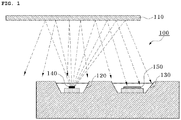
- FIG. 1 is a diagram illustrating a reflection type optical sensor device according to a related art.
- a known patent applying the reflection type optical sensor device of FIG. 1 disclosed is the Korean Patent Publication No. 10-2007-0088573 , titled “combined laser transmitter and photo-detector receiver package”.
- the known reflection type optical sensor device 100 includes a reflection type sensor package with a first cavity 120 and a second cavity 130 in order to detect the existence and absence of an object 110.
- a VCSEL 140 is located within the first cavity 120
- an optical receiver 150 is located within the second cavity 130.
- the optical receiver 150 is constructed to receive at least one portion of the light that is emitted from the VCSEL 140 and is reflected from the object 110. When the reflected light exceeds a predetermined threshold, it is determined that the object 110 exists.
- the light reflected from an object is not inclined to only one direction. Therefore, in the case of a known method where an optical receiver is provided in one direction only, it may cause an inaccurate detection.
- the volume of the reflection type optical sensor device may be enlarged and thus may be inapplicable.
- the present invention has been finalized in order to solve the above-described problem, and thus provides a reflection type optical sensor device where a semiconductor light source with a light emitting region and a photo-detection element with a light receiving region are integrated on a single chip.
- a reflection type optical sensor device as disclosed in claim 1, including: a semiconductor light source being formed by providing a light emitting region on a predetermined region of a substrate; and a photo-detection element being integrated on the same substrate as the substrate where the semiconductor light source is formed, to surround an outer circumferential surface of the semiconductor light source, and including a light receiving region, wherein, when the light emitted from the semiconductor light source is reflected by an external object, the photo-detection element detects the light to sense the object.
- a blocking layer is further provided in a predetermined region between the outer circumferential surface of the semiconductor light source and the photo-detection element.
- the semiconductor light sources may emit the light from a side opposite the substrate using a top emission scheme.
- the semiconductor light source may emit the light through a bottom surface of the substrate.
- a microlens may be further provided in a light emitting path of the semiconductor light source, and the micro lens may be integrated in an upper portion of the semiconductor light source.
- a microlens may be further provided in a light emitting path of the semiconductor light source, and the micro lens may be integrated in a bottom surface of the substrate where the semiconductor light source is formed.
- the semiconductor light source may include a first distributed Bragg reflector, the light emitting region, and a second distributed Bragg reflector from the substrate.
- the photo-detection element may include the first distributed Bragg reflector, the light receiving region, and the second distributed Bragg reflector from the substrate.
- a semiconductor light source with a light emitting region and a photo-detection element with a light receiving region is located on a single chip to thereby minimize the volume in the reflection type optical sensor device.
- the photo-detection element is provided to surround an outer circumferential surface of the semiconductor light source and thus may more accurately detect the light.
- FIG. 2A is a plan view for describing a reflection type optical sensor device according to an exemplary embodiment of the present invention
- FIG. 2B is a cross-sectional view cut along the I-I' line of FIG. 2A .
- the reflection type optical sensor device includes a semiconductor light source 210 and a photo-detection element 220.
- the semiconductor light source 210 and the photo-detection element 220 are provided on the same substrate.
- the photo-detection element 220 surrounds an outer circumferential surface of the semiconductor light source 210.
- a blocking layer B is further provided within a predetermined space formed between the outer circumferential surface of the semiconductor light source 210 and the photo-detection element 220 in order to block a spontaneous emission light emitted from the semiconductor light source 210.
- the light emitted from the semiconductor light source 210 may include the spontaneous emission light and a stimulated emission light.
- the semiconductor light source 210 uses, for example, a semiconductor laser and the like, most of the light may be the stimulated emission light and thus progress into the vertical direction, but the spontaneous emission light may also exist to some extents.
- the blocking layer B needs to be additionally provided.
- the blocking layer B may use, for example, a metal capable of absorbing the light, a polymer with a very weak permeability, and the like.
- the reflection type optical sensor device may include, for example, a substrate 230, a first distributed Bragg reflector (DBR) 240, n-type ohmic contact layers 250 and 250', active layers (that is, a light emitting region and light receiving regions) 260 and 260', p-type ohmic contact layers 270 and 270', and second DBRs 280 and 280'.
- DBR distributed Bragg reflector
- the reflection type optical sensor device includes a polymer layer P that is formed using a scheme of exposing an opening of the emitted light and an opening of received light to thereby cover the entire structure of the reflection type optical sensor device, for example, by applying a resin such as polyimide and the like to the entire structure of the reflection type optical sensor device.
- the substrate 230 may use, as a semiconductor substrate, an n-type semiconductor substrate, preferably, for example, a GaAs or InP based compound semiconductor.
- the type of substrate 230 is not particularly limited thereto.
- a glass substrate, a sapphire substrate, and the like may be used for the substrate 230.
- the first DBR 240, and the second DBRs 280 and 280' may be provided so that at least two material layers with a different refractive index, for example, a material layer with a high refractive index and a material layer with a low refractive index may be alternatively layered while having a predetermined thickness.
- the above first DBR 240 and the second DBRs 280 and 280' may adjust, for example, a reflection characteristic so that the light reflected from the light emitting region 260 may progress into an upper portion d or a lower portion of the first DBR 240 and the second DBRs 280 and 280'.
- first DBR 240 and the second DBRs 280 and 280' may adjust an amount of light emitted through the upper portion or the lower portion by adjusting a reflection ratio through an addition to or a subtraction from the number of layers.
- the light emitting region 260 denotes a region where a light emission occurs according to a recombination of electrons and holes that are supplied from a positive electrode and a negative electrode, respectively.
- the light emitting region 260 may be, for example, a bulk type, a semiconductor quantum well, a quantum dot, and the like.
- n-type electrodes 295 and 295', p-type electrodes 296 and 296', and the blocking layers B are provided in a predetermined region of the polymer layer P, through a metal depositing process, a patterning process, and the like, after a selective etching process.
- the substrate 230 for example, the n-type semiconductor substrate may be prepared by sequentially layering the first DRB 240, the n-type ohmic contact layers 250 and 250', the active layers (that is, the light emitting region and the light receiving region) 260 and 260', the p-type ohmic contact layers 270 and 270', and the second DBRs 280 and 280'.
- the second DBRs 280 and 280' may be selectively etched from an upper portion of the second DBRs 280 and 280'.
- the p-type ohmic contact layers 270 and 270', and the active layers 260 and 260' may be selectively etched.
- the n-type ohmic contact layers 250 and 250', and the first DBR 240 may be selectively etched.
- the polymer layer P may be formed using a scheme of exposing an opening of light emission and an opening of light receiving from the entire structure manufactured as above to thereby cover the entire structure of the reflection type optical sensor device, for example, by applying a resin such as polyimide and the like to the entire structure of the reflection type optical sensor device.
- the reflection type optical sensor device according to an embodiment of the present invention is completed.
- the semiconductor light source 210 and the photo-detection element 220 are integrated on a single chip. Unlike the related art shown in FIG. 1 , no cavity exists between the semiconductor light source 210 and the photo-detection element 220.
- the photo-detection element 220 surrounds the outer circumferential surface of the semiconductor light source 210, and thus may more effectively detect the light reflected from an object.
- the semiconductor light source 210 may be configured using a top emission scheme, that is, a scheme of emitting the light from a side opposite the substrate 230, or a scheme of emitting the light through bottom surface of the substrate 230.
- FIG. 3A is a plan view for describing a reflection type optical sensor device according to another exemplary embodiment of the present invention
- FIG. 3B is a cross-sectional view cut along the II-II' line of FIG. 3A .
- the reflection type optical sensor device may include a first DBR 240, n-type ohmic contact layers 250 and 250', active layers (that is, a light emitting region and light receiving regions) 260 and 260', p-type ohmic contact layers 270 and 270', second DBRs 280 and 280', n-type electrodes 295 and 295', p-type electrodes 296 and 296', and blocking layers B that are provided on a substrate 230, for example, an n-type semiconductor substrate.
- the reflection type optical sensor device further includes a polymer layer P that is formed using a scheme of exposing an opening of light emission and an opening of light receiving to thereby cover the entire structure of the reflection type optical sensor device, for example, by applying a resin such as polyimide and the like to the entire structure of the reflection type optical sensor device.
- a micro lens L is integrated in an upper portion of the semiconductor light source 210 as shown in FIGS. 3A and 3B .
- the micro lens L may be selectively integrated in the upper portion of the semiconductor light source 210, which may be easily performed in the manufacturing operation of the reflection type optical sensor. Also, the manufacturing method of the micro lens L is not particularly limited and thus may be performed using various types of schemes.
- the micro lens L may be manufactured using a method disclosed in Korean Patent Publication No. 10-2006-0043912 , titled “Method for Manufacturing Micro Lens Integrated Optoelectronic Device", or Korean Patent Publication No. 10-2007-0055764 , titled “Method for Fabricating Micro-lens and Micro-lens Integrated Optoelectronic Devices Using Selective Etch of Compound Semiconductor", filed by the same inventor of this invention.
- the first DBR 240, the n-type ohmic contact layers 250 and 250', the active layers (that is, the light emitting region and the light receiving region) 260 and 260', the p-type ohmic contact layers 270 and 270', and the second DBRs 280 and 280' may be sequentially layered on the substrate 230, for example, the n-type semiconductor substrate as shown in FIG. 3B .
- a probable compound semiconductor oxide layer 310 is formed in order to manufacture the micro lens L, for example, while gradually increasing a ratio of aluminum.
- portions 320 and 330 may function as a lens to form the micro lens L.
- a focal distance of the micro lens L may be changed by adjusting, for example, an oxidization time, a temperature, a growth condition of a possible oxide layer, and the like.
- FIG. 4A is a plan view for describing a reflection type optical sensor device according to still another exemplary embodiment of the present invention
- FIG. 4B is a cross-sectional view cut along the III-III' line of FIG. 4A .
- the reflection type optical sensor device may include a first DBR 240, n-type ohmic contact layers 250 and 250', active layers (that is, a light emitting region and light receiving regions) 260 and 260', p-type ohmic contact layers 270 and 270', second DBRs 280 and 280', n-type electrodes 295 and 295', p-type electrodes 296 and 296', and blocking layers B that are provided on a substrate 230, for example, an n-type semiconductor substrate.
- the reflection type optical sensor device further includes a polymer layer P that is formed using a scheme of exposing an opening of emitted light and an opening of received light to thereby cover the entire structure of the reflection type optical sensor device, for example, by applying a resin such as polyimide and the like to the entire structure of the reflection type optical sensor device.
- a micro lens L is integrated in a lower portion of the substrate 230 as shown in FIGS. 4A and 4B .
- FIGS. 4A and 4B The above structure shown in FIGS. 4A and 4B is different from the structure of the reflection type optical sensor device described above with reference to FIGS. 3A and 3B .
- the micro lens L is provided in the upper portion of the semiconductor light source 210 in FIGS. 3A and 3B , whereas the micro lens L is provided in the lower portion of the substrate 230, that is, the lower portion of the substrate 230 where the semiconductor light source 210 is formed in FIGS. 4A and 4B .
- FIGS. 2A to 3B illustrate a case where the light emitted from the semiconductor light source 210 is emitted from a side opposite the substrate 230.
- FIGS. 4A and 4B illustrate a case where the light emitted from the semiconductor light source 210 is emitted through a bottom surface of the substrate 230.
- the semiconductor light source 210 of FIGS. 4A and 4B has a structural difference from the semiconductor light source 210 of FIGS. 2A through 3B in order to emit the light through the bottom surface of the substrate 230.
- the first DBR 240 and the second DBRs 280 and 280' may adjust each reflection characteristic so that the light emitted from the light emitting region 260 may progress into the lower portion of the substrate 230.
- a scheme of forming the micro lens L in the lower portion of the substrate 230 may use, for example, a reflow scheme, and the like.
- a desired size of a cylindrical photoresist pattern may be formed in the lower portion of the substrate 230, for example, using a photo lithography scheme, and the like.
- the cylindrical photoresist pattern when heated and is reflowed, the cylindrical photoresist may become thinner while approaching an edge region from a central axis due to a surface tension and thereby may be changed into a convex lens having a radius of curvature.
- the micro lens L may be formed in a predetermined region of the lower portion of the substrate 230, that is, in the lower portion of the substrate 230 corresponding to where the semiconductor light source 210 is formed.
- the emitted light is enabled to progress via the micro lens L. Through this, it is possible to decrease a beam divergence.
Landscapes
- Photo Coupler, Interrupter, Optical-To-Optical Conversion Devices (AREA)
- Semiconductor Lasers (AREA)
- Optical Head (AREA)
- Light Receiving Elements (AREA)
- Led Device Packages (AREA)
Description
- The present invention relates to a reflection type optical sensor device, and more particularly, to a reflection type optical sensor device that may integrate, on a single chip, a semiconductor light source and a photo-detection element that are used for a reflection type optical sensor device, in order to more accurately detect the light.
- Generally, a reflection type optical sensor includes a light emitter and a light receiver on the same side of an object for detection. The existence of the object may be detected when the light emitted from the light emitter is reflected from the surface of the object and is received by the optical receiver.
- Known reflection type optical sensors include a light-emitting diode and an optical receiver installed within a cavity. However, the light of the luminescent diode may cause an inaccurate detection due to its low intensity and excessive crosstalk.
- Accordingly, a reflection type optical sensor using a vertical cavity surface emitting laser (VCSEL) is currently being used instead of the luminescent diode.
-
FIG. 1 is a diagram illustrating a reflection type optical sensor device according to a related art. As a known patent applying the reflection type optical sensor device ofFIG. 1 , disclosed is the Korean Patent Publication No.10-2007-0088573 - Referring to
FIG. 1 , the known reflection typeoptical sensor device 100 includes a reflection type sensor package with afirst cavity 120 and asecond cavity 130 in order to detect the existence and absence of anobject 110. In order to emit the light, aVCSEL 140 is located within thefirst cavity 120, and anoptical receiver 150 is located within thesecond cavity 130. - In this instance, the
optical receiver 150 is constructed to receive at least one portion of the light that is emitted from the VCSEL 140 and is reflected from theobject 110. When the reflected light exceeds a predetermined threshold, it is determined that theobject 110 exists. - The light reflected from an object is not inclined to only one direction. Therefore, in the case of a known method where an optical receiver is provided in one direction only, it may cause an inaccurate detection.
- Also, in the known method of separately providing a light emitter and an optical receiver, when a reflection type optical sensor device is installed in a compact portable device such as a mobile phone and the like, the volume of the reflection type optical sensor device may be enlarged and thus may be inapplicable.
- The present invention has been finalized in order to solve the above-described problem, and thus provides a reflection type optical sensor device where a semiconductor light source with a light emitting region and a photo-detection element with a light receiving region are integrated on a single chip.
- According to an aspect of the present invention, there is provided a reflection type optical sensor device as disclosed in claim 1, including: a semiconductor light source being formed by providing a light emitting region on a predetermined region of a substrate; and a photo-detection element being integrated on the same substrate as the substrate where the semiconductor light source is formed, to surround an outer circumferential surface of the semiconductor light source, and including a light receiving region, wherein, when the light emitted from the semiconductor light source is reflected by an external object, the photo-detection element detects the light to sense the object.
- In this instance, a blocking layer is further provided in a predetermined region between the outer circumferential surface of the semiconductor light source and the photo-detection element.
- Also, the semiconductor light sources may emit the light from a side opposite the substrate using a top emission scheme.
- Also, the semiconductor light source may emit the light through a bottom surface of the substrate.
- Also, a microlens may be further provided in a light emitting path of the semiconductor light source, and the micro lens may be integrated in an upper portion of the semiconductor light source.
- Also, a microlens may be further provided in a light emitting path of the semiconductor light source, and the micro lens may be integrated in a bottom surface of the substrate where the semiconductor light source is formed.
- Also, the semiconductor light source may include a first distributed Bragg reflector, the light emitting region, and a second distributed Bragg reflector from the substrate. The photo-detection element may include the first distributed Bragg reflector, the light receiving region, and the second distributed Bragg reflector from the substrate.
- According to a reflection type optical sensor device of the present invention, a semiconductor light source with a light emitting region and a photo-detection element with a light receiving region is located on a single chip to thereby minimize the volume in the reflection type optical sensor device. Also, according to exemplary embodiments of the present invention, the photo-detection element is provided to surround an outer circumferential surface of the semiconductor light source and thus may more accurately detect the light.
-
-
FIG. 1 is a diagram illustrating a reflection type optical sensor device according to a related art; -
FIG. 2A is a plan view for describing a reflection type optical sensor device according to an exemplary embodiment of the present invention; -
FIG. 2B is a cross-sectional view cut along the I-I' line ofFIG. 2A ; -
FIG. 3A is a plan view for describing a reflection type optical sensor device according to another exemplary embodiment of the present invention; -
FIG. 3B is a cross-sectional view cut along the II-II' line ofFIG. 3A ; -
FIG. 4A is a plan view for describing a reflection type optical sensor device according to still another exemplary embodiment of the present invention; and -
FIG. 4B is a cross-sectional view cut along the III-III' line ofFIG. 4A . - Reference will now be made in detail to exemplary embodiments of the present invention, examples of which are illustrated in the accompanying drawings, wherein like reference numerals refer to like elements throughout. Exemplary embodiments are described below to explain the present invention by referring to the figures.
-
FIG. 2A is a plan view for describing a reflection type optical sensor device according to an exemplary embodiment of the present invention, andFIG. 2B is a cross-sectional view cut along the I-I' line ofFIG. 2A . - Referring to
FIG. 2A , the reflection type optical sensor device according to an exemplary embodiment of the present invention includes asemiconductor light source 210 and a photo-detection element 220. - In
FIG. 2A , thesemiconductor light source 210 and the photo-detection element 220 are provided on the same substrate. The photo-detection element 220 surrounds an outer circumferential surface of thesemiconductor light source 210. - In this instance, a blocking layer B is further provided within a predetermined space formed between the outer circumferential surface of the
semiconductor light source 210 and the photo-detection element 220 in order to block a spontaneous emission light emitted from thesemiconductor light source 210. - Specifically, the light emitted from the
semiconductor light source 210 may include the spontaneous emission light and a stimulated emission light. When thesemiconductor light source 210 uses, for example, a semiconductor laser and the like, most of the light may be the stimulated emission light and thus progress into the vertical direction, but the spontaneous emission light may also exist to some extents. - In this instance, when the spontaneous emission light enters a predetermined portion of the photo-
detection element 220, noise may occur. Accordingly, there is a need to prevent the spontaneous emission light from entering the photo-detection element 220. For this, the blocking layer B needs to be additionally provided. - The blocking layer B may use, for example, a metal capable of absorbing the light, a polymer with a very weak permeability, and the like.
- Referring to
FIG. 2B , the reflection type optical sensor device according to an exemplary embodiment of the present invention may include, for example, asubstrate 230, a first distributed Bragg reflector (DBR) 240, n-type ohmic contact layers 250 and 250', active layers (that is, a light emitting region and light receiving regions) 260 and 260', p-type ohmic contact layers 270 and 270', and second DBRs 280 and 280'. - Also, the reflection type optical sensor device includes a polymer layer P that is formed using a scheme of exposing an opening of the emitted light and an opening of received light to thereby cover the entire structure of the reflection type optical sensor device, for example, by applying a resin such as polyimide and the like to the entire structure of the reflection type optical sensor device.
- Here, the
substrate 230 may use, as a semiconductor substrate, an n-type semiconductor substrate, preferably, for example, a GaAs or InP based compound semiconductor. - Also, when the reflection type optical sensor device according to an embodiment of the present invention is applicable, the type of
substrate 230 is not particularly limited thereto. When necessary, for example, a glass substrate, a sapphire substrate, and the like may be used for thesubstrate 230. - The
first DBR 240, and the second DBRs 280 and 280' may be provided so that at least two material layers with a different refractive index, for example, a material layer with a high refractive index and a material layer with a low refractive index may be alternatively layered while having a predetermined thickness. - The above
first DBR 240 and the second DBRs 280 and 280' may adjust, for example, a reflection characteristic so that the light reflected from thelight emitting region 260 may progress into an upper portion d or a lower portion of thefirst DBR 240 and the second DBRs 280 and 280'. - Also, the
first DBR 240 and the second DBRs 280 and 280' may adjust an amount of light emitted through the upper portion or the lower portion by adjusting a reflection ratio through an addition to or a subtraction from the number of layers. - The
light emitting region 260 denotes a region where a light emission occurs according to a recombination of electrons and holes that are supplied from a positive electrode and a negative electrode, respectively. Thelight emitting region 260 may be, for example, a bulk type, a semiconductor quantum well, a quantum dot, and the like. - Finally, n-
type electrodes 295 and 295', p-type electrodes 296 and 296', and the blocking layers B are provided in a predetermined region of the polymer layer P, through a metal depositing process, a patterning process, and the like, after a selective etching process. - Hereinafter, an example of a method for manufacturing a reflection type optical sensor device according to an embodiment of the present invention will be described in detail with reference to
FIG. 2B . - Referring to
FIG. 2B , thesubstrate 230, for example, the n-type semiconductor substrate may be prepared by sequentially layering thefirst DRB 240, the n-type ohmic contact layers 250 and 250', the active layers (that is, the light emitting region and the light receiving region) 260 and 260', the p-type ohmic contact layers 270 and 270', and the second DBRs 280 and 280'. - Next, the second DBRs 280 and 280' may be selectively etched from an upper portion of the second DBRs 280 and 280'. The p-type ohmic contact layers 270 and 270', and the
active layers 260 and 260' may be selectively etched. Next, the n-type ohmic contact layers 250 and 250', and thefirst DBR 240 may be selectively etched. - Next, the polymer layer P may be formed using a scheme of exposing an opening of light emission and an opening of light receiving from the entire structure manufactured as above to thereby cover the entire structure of the reflection type optical sensor device, for example, by applying a resin such as polyimide and the like to the entire structure of the reflection type optical sensor device.
- Next, when a predetermined region of the polymer layer P is selectively etched and then the n-
type electrodes 295 and 295', the p-type electrodes 296 and 296', and the blocking layers B are formed through the metal depositing process and the patterning process, then the reflection type optical sensor device according to an embodiment of the present invention is completed. - In the reflection type optical sensor device constructed as above, the
semiconductor light source 210 and the photo-detection element 220 are integrated on a single chip. Unlike the related art shown inFIG. 1 , no cavity exists between thesemiconductor light source 210 and the photo-detection element 220. - Also, the photo-
detection element 220 surrounds the outer circumferential surface of thesemiconductor light source 210, and thus may more effectively detect the light reflected from an object. - In this instance, the
semiconductor light source 210 may be configured using a top emission scheme, that is, a scheme of emitting the light from a side opposite thesubstrate 230, or a scheme of emitting the light through bottom surface of thesubstrate 230. -
FIG. 3A is a plan view for describing a reflection type optical sensor device according to another exemplary embodiment of the present invention, andFIG. 3B is a cross-sectional view cut along the II-II' line ofFIG. 3A . - Referring to
FIGS. 3A and 3B , the reflection type optical sensor device according to another exemplary embodiment of the present invention may include afirst DBR 240, n-type ohmic contact layers 250 and 250', active layers (that is, a light emitting region and light receiving regions) 260 and 260', p-type ohmic contact layers 270 and 270',second DBRs 280 and 280', n-type electrodes 295 and 295', p-type electrodes 296 and 296', and blocking layers B that are provided on asubstrate 230, for example, an n-type semiconductor substrate. - Also, the reflection type optical sensor device further includes a polymer layer P that is formed using a scheme of exposing an opening of light emission and an opening of light receiving to thereby cover the entire structure of the reflection type optical sensor device, for example, by applying a resin such as polyimide and the like to the entire structure of the reflection type optical sensor device.
- Describing the difference between the reflection type optical sensor device according to another exemplary embodiment of the present invention and the reflection type optical sensor device described above with reference to
FIGS. 2A and 2B , a micro lens L is integrated in an upper portion of thesemiconductor light source 210 as shown inFIGS. 3A and 3B . - In this instance, the micro lens L may be selectively integrated in the upper portion of the
semiconductor light source 210, which may be easily performed in the manufacturing operation of the reflection type optical sensor. Also, the manufacturing method of the micro lens L is not particularly limited and thus may be performed using various types of schemes. - For example, the micro lens L may be manufactured using a method disclosed in Korean Patent Publication No.
10-2006-0043912 10-2007-0055764 - Further, with reference to the method disclosed in Korean Patent Publication No.
10-2006-0043912 first DBR 240, the n-type ohmic contact layers 250 and 250', the active layers (that is, the light emitting region and the light receiving region) 260 and 260', the p-type ohmic contact layers 270 and 270', and the second DBRs 280 and 280' may be sequentially layered on thesubstrate 230, for example, the n-type semiconductor substrate as shown inFIG. 3B . - Next, a probable compound
semiconductor oxide layer 310 is formed in order to manufacture the micro lens L, for example, while gradually increasing a ratio of aluminum. - Next, when the oxidization is performed at a high temperature, a
portion 320 where the ratio of aluminum is high may be oxidized whereby a refractive index decreases. Aportion 330 where the ratio of aluminum is low may remain in an original compound semiconductor state and thereby have a high refractive index. As a result,portions - In this instance, a focal distance of the micro lens L may be changed by adjusting, for example, an oxidization time, a temperature, a growth condition of a possible oxide layer, and the like.
-
FIG. 4A is a plan view for describing a reflection type optical sensor device according to still another exemplary embodiment of the present invention, andFIG. 4B is a cross-sectional view cut along the III-III' line ofFIG. 4A . - Referring to
FIGS. 4A and 4B , the reflection type optical sensor device according to still another exemplary embodiment of the present invention may include afirst DBR 240, n-type ohmic contact layers 250 and 250', active layers (that is, a light emitting region and light receiving regions) 260 and 260', p-type ohmic contact layers 270 and 270',second DBRs 280 and 280', n-type electrodes 295 and 295', p-type electrodes 296 and 296', and blocking layers B that are provided on asubstrate 230, for example, an n-type semiconductor substrate. - Also, the reflection type optical sensor device further includes a polymer layer P that is formed using a scheme of exposing an opening of emitted light and an opening of received light to thereby cover the entire structure of the reflection type optical sensor device, for example, by applying a resin such as polyimide and the like to the entire structure of the reflection type optical sensor device.
- Describing the difference between the reflection type optical sensor device according to still another exemplary embodiment of the present invention and the reflection type optical sensor device described above with reference to
FIGS. 2A and 2B , a micro lens L is integrated in a lower portion of thesubstrate 230 as shown inFIGS. 4A and 4B . - The above structure shown in
FIGS. 4A and 4B is different from the structure of the reflection type optical sensor device described above with reference toFIGS. 3A and 3B . - Specifically, the micro lens L is provided in the upper portion of the
semiconductor light source 210 inFIGS. 3A and 3B , whereas the micro lens L is provided in the lower portion of thesubstrate 230, that is, the lower portion of thesubstrate 230 where thesemiconductor light source 210 is formed inFIGS. 4A and 4B . -
FIGS. 2A to 3B illustrate a case where the light emitted from thesemiconductor light source 210 is emitted from a side opposite thesubstrate 230.FIGS. 4A and 4B illustrate a case where the light emitted from thesemiconductor light source 210 is emitted through a bottom surface of thesubstrate 230. - Accordingly, the
semiconductor light source 210 ofFIGS. 4A and 4B has a structural difference from thesemiconductor light source 210 ofFIGS. 2A through 3B in order to emit the light through the bottom surface of thesubstrate 230. - For example, the
first DBR 240 and the second DBRs 280 and 280' may adjust each reflection characteristic so that the light emitted from thelight emitting region 260 may progress into the lower portion of thesubstrate 230. - A scheme of forming the micro lens L in the lower portion of the
substrate 230 may use, for example, a reflow scheme, and the like. - In order to form the micro lens L in the lower portion of the
substrate 230 through the reflow scheme, a desired size of a cylindrical photoresist pattern may be formed in the lower portion of thesubstrate 230, for example, using a photo lithography scheme, and the like. - Next, when the cylindrical photoresist pattern is heated and is reflowed, the cylindrical photoresist may become thinner while approaching an edge region from a central axis due to a surface tension and thereby may be changed into a convex lens having a radius of curvature.
- Next, when the photoresist in the lens form is etched using a mask, for example, a dry etching scheme, and the like, the micro lens L may be formed in a predetermined region of the lower portion of the
substrate 230, that is, in the lower portion of thesubstrate 230 corresponding to where thesemiconductor light source 210 is formed. - When the light emitted from the
light emitting region 260 of thesemiconductor light source 210 is emitted through an opening, the emitted light is enabled to progress via the micro lens L. Through this, it is possible to decrease a beam divergence.
Claims (6)
- A reflection type optical sensor device comprising:a semiconductor light source (210) being formed by providing a light emitting region (260) on a predetermined region of a substrate (230); anda photo-detection element (220) being integrated on the same substrate as the substrate where the semiconductor light source is formed, to surround an outer circumferential surface of the semiconductor light source, and including a light receiving region (260') a light blocking layer (B) and a polymer layer (P) which are formed within a space between the semiconductor light source and the photo-detection element, wherein the blocking layer and the polymer fill the space,wherein, when the light emitted from the semiconductor light source is reflected by an external object, the photo-detection element detects the light to sense the object.
- The reflection type optical sensor device of claim 1, wherein the semiconductor light sources emits the light from a side opposite the substrate using a top emission scheme.
- The reflection type optical sensor device of claim 1, wherein the semiconductor light source emits the light through a bottom surface of the substrate.
- The reflection type optical sensor device of claim 1, wherein a micro lens (L) is further provided in a light emitting path of the semiconductor light source, and the micro lens is integrated in an upper portion of the semiconductor light source.
- The reflection type optical sensor device of claim 1, wherein a micro lens is further provided in a light emitting path of the semiconductor light source, and the micro lens (L) is integrated in a lower portion of the substrate where the semiconductor light source is formed.
- The reflection type optical sensor device of claim 1, wherein:the semiconductor light source comprises a first distributed Bragg reflector (240), the light emitting region (260), and a second distributed Bragg reflector (280) from the substrate, andthe photo-detection element comprises the first distributed Bragg reflector (240), the light receiving region (260'), and the second distributed Bragg reflector (280') from the substrate.
Applications Claiming Priority (1)
| Application Number | Priority Date | Filing Date | Title |
|---|---|---|---|
| KR1020080047166A KR101360294B1 (en) | 2008-05-21 | 2008-05-21 | A reflection type optics sensor device |
Publications (3)
| Publication Number | Publication Date |
|---|---|
| EP2124263A2 EP2124263A2 (en) | 2009-11-25 |
| EP2124263A3 EP2124263A3 (en) | 2012-11-07 |
| EP2124263B1 true EP2124263B1 (en) | 2017-05-03 |
Family
ID=41056976
Family Applications (1)
| Application Number | Title | Priority Date | Filing Date |
|---|---|---|---|
| EP09160742.4A Not-in-force EP2124263B1 (en) | 2008-05-21 | 2009-05-20 | Reflection type optical sensor device |
Country Status (4)
| Country | Link |
|---|---|
| US (1) | US7982226B2 (en) |
| EP (1) | EP2124263B1 (en) |
| JP (1) | JP5175243B2 (en) |
| KR (1) | KR101360294B1 (en) |
Families Citing this family (26)
| Publication number | Priority date | Publication date | Assignee | Title |
|---|---|---|---|---|
| US8395226B2 (en) * | 2009-01-27 | 2013-03-12 | Insiava (Pty) Limited | Microchip-based MOEMS and waveguide device |
| DE112011105262B4 (en) * | 2011-05-19 | 2025-10-16 | OSRAM Opto Semiconductors Gesellschaft mit beschränkter Haftung | Optoelectronic device and method for producing optoelectronic devices |
| US8796724B2 (en) | 2011-12-20 | 2014-08-05 | Todd W Hodrinsky | Light emitting systems and methods |
| JP6006108B2 (en) * | 2012-12-20 | 2016-10-12 | 株式会社アルファ | Optical sensor unit |
| US9018645B2 (en) * | 2013-08-29 | 2015-04-28 | Stmicroelectronics Pte Ltd | Optoelectronics assembly and method of making optoelectronics assembly |
| JP6550381B2 (en) | 2013-10-16 | 2019-07-24 | コーニンクレッカ フィリップス エヌ ヴェKoninklijke Philips N.V. | Compact laser device |
| US20150330897A1 (en) * | 2014-05-14 | 2015-11-19 | Semiconductor Components Industries, Llc | Image sensor and method for measuring refractive index |
| JP6380973B2 (en) * | 2014-06-16 | 2018-08-29 | 日東電工株式会社 | Optical sensor |
| EP3176888A1 (en) * | 2015-12-03 | 2017-06-07 | Koninklijke Philips N.V. | Sensor chip |
| JP6786798B2 (en) * | 2015-12-22 | 2020-11-18 | 株式会社リコー | Optical sensor, optical inspection device, and optical characteristic detection method |
| US11031751B2 (en) * | 2016-08-10 | 2021-06-08 | Hamamatsu Photonics K.K. | Light-emitting device |
| JP6747910B2 (en) * | 2016-08-10 | 2020-08-26 | 浜松ホトニクス株式会社 | Light emitting device |
| US10734786B2 (en) | 2016-09-07 | 2020-08-04 | Hamamatsu Photonics K.K. | Semiconductor light emitting element and light emitting device including same |
| US11646546B2 (en) | 2017-03-27 | 2023-05-09 | Hamamatsu Photonics K.K. | Semiconductor light emitting array with phase modulation regions for generating beam projection patterns |
| US11637409B2 (en) | 2017-03-27 | 2023-04-25 | Hamamatsu Photonics K.K. | Semiconductor light-emitting module and control method therefor |
| JP6959042B2 (en) | 2017-06-15 | 2021-11-02 | 浜松ホトニクス株式会社 | Light emitting device |
| US10928438B2 (en) | 2017-07-20 | 2021-02-23 | International Business Machines Corporation | Embedded photodetector as device health monitor for hot carrier injection (HCI) in power semiconductors |
| US11626709B2 (en) | 2017-12-08 | 2023-04-11 | Hamamatsu Photonics K.K. | Light-emitting device and production method for same |
| CN112272906B (en) | 2018-06-08 | 2024-03-15 | 浜松光子学株式会社 | Light-emitting element |
| US20200035862A1 (en) * | 2018-07-26 | 2020-01-30 | Bolb Inc. | Light-emitting device with optical power readout |
| US10811400B2 (en) * | 2018-09-28 | 2020-10-20 | Apple Inc. | Wafer level optical module |
| US12074408B2 (en) * | 2019-10-01 | 2024-08-27 | Meta Platforms Technologies, Llc | Vertical cavity surface-emitting laser (VCSEL) with a light barrier |
| EP3901612B1 (en) * | 2020-04-23 | 2024-06-12 | Sensirion AG | Integrated particulate matter sensor with cavity |
| TWI865899B (en) | 2022-08-02 | 2024-12-11 | 鴻海精密工業股份有限公司 | Micro led display device |
| CN115064564A (en) * | 2022-08-02 | 2022-09-16 | 鸿海精密工业股份有限公司 | Micro light-emitting diode display device |
| US12399340B2 (en) | 2022-10-27 | 2025-08-26 | Sensirion Ag | Optical component, optoelectronic module and method of manufacture |
Family Cites Families (19)
| Publication number | Priority date | Publication date | Assignee | Title |
|---|---|---|---|---|
| JPS5440907B1 (en) * | 1969-06-02 | 1979-12-05 | ||
| DE2425855C2 (en) * | 1974-05-28 | 1982-09-23 | Licentia Patent-Verwaltungs-Gmbh, 6000 Frankfurt | Photoelectric reading unit for reading optically scannable documents |
| JPS5967671A (en) * | 1982-10-12 | 1984-04-17 | Nec Corp | Light emitting light receiving element |
| JPS59129467A (en) * | 1983-01-14 | 1984-07-25 | Toshiba Corp | Composite optical semiconductor element |
| JPS61265742A (en) * | 1985-05-20 | 1986-11-25 | Nippon Telegr & Teleph Corp <Ntt> | Optical head |
| JPH0758767B2 (en) * | 1988-10-17 | 1995-06-21 | 沖電気工業株式会社 | Perfect contact image sensor |
| JP2879971B2 (en) * | 1990-11-30 | 1999-04-05 | 株式会社日立製作所 | Light emitting and receiving composite element |
| JP3122710B2 (en) * | 1995-03-10 | 2001-01-09 | オリンパス光学工業株式会社 | Surface emitting semiconductor laser and optical encoder using the same |
| KR100259490B1 (en) * | 1995-04-28 | 2000-06-15 | 윤종용 | Photodetector integrated surface light laser and optical pickup device using same |
| JPH0945995A (en) * | 1995-07-26 | 1997-02-14 | Sony Corp | Optical device |
| JPH0983084A (en) * | 1995-09-19 | 1997-03-28 | Olympus Optical Co Ltd | Semiconductor laser |
| US5648979A (en) * | 1995-12-29 | 1997-07-15 | Samsung Electronics Co. Ltd. | Assembly of VCSEL light source and VCSEL optical detector |
| JP3002180B1 (en) | 1998-07-13 | 2000-01-24 | 松下電子工業株式会社 | Optical semiconductor device |
| JP2002374039A (en) * | 2001-02-27 | 2002-12-26 | Ricoh Co Ltd | Optical transmitting / receiving system and optical communication system |
| KR100657252B1 (en) * | 2000-01-20 | 2006-12-14 | 삼성전자주식회사 | Near-field recording and reproducing optical head and its manufacturing method |
| JP2001155366A (en) | 2000-10-04 | 2001-06-08 | Hitachi Ltd | Optical head and method of manufacturing optical head |
| JP2004235190A (en) * | 2003-01-28 | 2004-08-19 | Sony Corp | Optical semiconductor device |
| JP2005064183A (en) | 2003-08-11 | 2005-03-10 | Murata Mfg Co Ltd | Reflecting sensor |
| US7489401B2 (en) * | 2004-03-01 | 2009-02-10 | National Institute Of Advanced Industrial Science And Technology | Device for detecting emission light of micro-object |
-
2008
- 2008-05-21 KR KR1020080047166A patent/KR101360294B1/en not_active Expired - Fee Related
-
2009
- 2009-05-19 US US12/468,664 patent/US7982226B2/en not_active Expired - Fee Related
- 2009-05-20 EP EP09160742.4A patent/EP2124263B1/en not_active Not-in-force
- 2009-05-21 JP JP2009122952A patent/JP5175243B2/en not_active Expired - Fee Related
Non-Patent Citations (1)
| Title |
|---|
| None * |
Also Published As
| Publication number | Publication date |
|---|---|
| EP2124263A2 (en) | 2009-11-25 |
| JP5175243B2 (en) | 2013-04-03 |
| EP2124263A3 (en) | 2012-11-07 |
| US7982226B2 (en) | 2011-07-19 |
| JP2009283941A (en) | 2009-12-03 |
| KR20090121057A (en) | 2009-11-25 |
| US20090289266A1 (en) | 2009-11-26 |
| KR101360294B1 (en) | 2014-02-11 |
Similar Documents
| Publication | Publication Date | Title |
|---|---|---|
| EP2124263B1 (en) | Reflection type optical sensor device | |
| US7085300B2 (en) | Integral vertical cavity surface emitting laser and power monitor | |
| US8243767B2 (en) | Vertical-cavity surface-emitting laser (VCSEL) device and the method of manufacturing thereof | |
| KR102113257B1 (en) | Apparatus of outputting directional light and light interconnection system having the same | |
| JP2006049829A (en) | Surface emitting semiconductor laser and manufacturing method of the same | |
| KR20190008562A (en) | A light emitting diode (LED) with integrated photodetectors for in situ real-time intensity monitoring, | |
| TWI645637B (en) | Vertical cavity surface emitting laser and method for fabricating the same | |
| CN100407525C (en) | Surface emitting semiconductor laser and manufacturing method thereof | |
| JP6206669B2 (en) | Surface emitting semiconductor laser, surface emitting semiconductor laser array, method for manufacturing surface emitting semiconductor laser, surface emitting semiconductor laser device, optical transmission device, and information processing device | |
| US7871841B2 (en) | Method for manufacturing semiconductor light-emitting device | |
| KR20010045739A (en) | Surface emitting laser with a monolithically integrated monitor photdetector | |
| CN113764977B (en) | Vertical Cavity Surface Emitting Laser with Integrated Photodiode | |
| TWM588387U (en) | Electrically pumped photonic crystal surface-emitting laser element with light detection structure | |
| US20240204479A1 (en) | Vertical cavity surface emitting laser (vcsel), laser sensor and method of producing a vcsel | |
| US12034271B2 (en) | Optoelectronic semiconductor device with first and second optoelectronic elements | |
| JP4019284B2 (en) | Surface emitting device and method for manufacturing the same | |
| KR102569495B1 (en) | A surface-emitting laser device and light emitting device including the same | |
| KR102563217B1 (en) | A surface-emitting laser device and light emitting device including the same | |
| KR102645382B1 (en) | A surface-emitting laser device and light emitting device including the same | |
| KR102504307B1 (en) | A surface-emitting laser device, light emitting device including the same and manufacturing method of the same | |
| KR100821359B1 (en) | Optical steering sensor device and optical module using same | |
| KR20220041215A (en) | Optoelectronic semiconductor chip comprising contact element and method of manufacturing optoelectronic semiconductor chip | |
| US6621844B1 (en) | Buried oxide photonic device with large contact and precise aperture | |
| CN115799994A (en) | Light emitting device | |
| CN119866427A (en) | VCSEL element, sensor device, electronic device and user interface |
Legal Events
| Date | Code | Title | Description |
|---|---|---|---|
| PUAI | Public reference made under article 153(3) epc to a published international application that has entered the european phase |
Free format text: ORIGINAL CODE: 0009012 |
|
| 17P | Request for examination filed |
Effective date: 20090520 |
|
| AK | Designated contracting states |
Kind code of ref document: A2 Designated state(s): AT BE BG CH CY CZ DE DK EE ES FI FR GB GR HR HU IE IS IT LI LT LU LV MC MK MT NL NO PL PT RO SE SI SK TR |
|
| PUAL | Search report despatched |
Free format text: ORIGINAL CODE: 0009013 |
|
| AK | Designated contracting states |
Kind code of ref document: A3 Designated state(s): AT BE BG CH CY CZ DE DK EE ES FI FR GB GR HR HU IE IS IT LI LT LU LV MC MK MT NL NO PL PT RO SE SI SK TR |
|
| RIC1 | Information provided on ipc code assigned before grant |
Ipc: H01L 31/173 20060101AFI20120928BHEP Ipc: H01L 31/0232 20060101ALI20120928BHEP Ipc: H01S 5/026 20060101ALN20120928BHEP Ipc: H01L 27/15 20060101ALI20120928BHEP |
|
| GRAP | Despatch of communication of intention to grant a patent |
Free format text: ORIGINAL CODE: EPIDOSNIGR1 |
|
| INTG | Intention to grant announced |
Effective date: 20170207 |
|
| GRAS | Grant fee paid |
Free format text: ORIGINAL CODE: EPIDOSNIGR3 |
|
| GRAA | (expected) grant |
Free format text: ORIGINAL CODE: 0009210 |
|
| AK | Designated contracting states |
Kind code of ref document: B1 Designated state(s): AT BE BG CH CY CZ DE DK EE ES FI FR GB GR HR HU IE IS IT LI LT LU LV MC MK MT NL NO PL PT RO SE SI SK TR |
|
| REG | Reference to a national code |
Ref country code: GB Ref legal event code: FG4D |
|
| REG | Reference to a national code |
Ref country code: AT Ref legal event code: REF Ref document number: 890862 Country of ref document: AT Kind code of ref document: T Effective date: 20170515 Ref country code: CH Ref legal event code: EP |
|
| REG | Reference to a national code |
Ref country code: IE Ref legal event code: FG4D |
|
| REG | Reference to a national code |
Ref country code: DE Ref legal event code: R096 Ref document number: 602009045802 Country of ref document: DE |
|
| REG | Reference to a national code |
Ref country code: NL Ref legal event code: MP Effective date: 20170503 |
|
| REG | Reference to a national code |
Ref country code: AT Ref legal event code: MK05 Ref document number: 890862 Country of ref document: AT Kind code of ref document: T Effective date: 20170503 |
|
| REG | Reference to a national code |
Ref country code: LT Ref legal event code: MG4D |
|
| PG25 | Lapsed in a contracting state [announced via postgrant information from national office to epo] |
Ref country code: HR Free format text: LAPSE BECAUSE OF FAILURE TO SUBMIT A TRANSLATION OF THE DESCRIPTION OR TO PAY THE FEE WITHIN THE PRESCRIBED TIME-LIMIT Effective date: 20170503 Ref country code: LT Free format text: LAPSE BECAUSE OF FAILURE TO SUBMIT A TRANSLATION OF THE DESCRIPTION OR TO PAY THE FEE WITHIN THE PRESCRIBED TIME-LIMIT Effective date: 20170503 Ref country code: GR Free format text: LAPSE BECAUSE OF FAILURE TO SUBMIT A TRANSLATION OF THE DESCRIPTION OR TO PAY THE FEE WITHIN THE PRESCRIBED TIME-LIMIT Effective date: 20170804 Ref country code: ES Free format text: LAPSE BECAUSE OF FAILURE TO SUBMIT A TRANSLATION OF THE DESCRIPTION OR TO PAY THE FEE WITHIN THE PRESCRIBED TIME-LIMIT Effective date: 20170503 Ref country code: FI Free format text: LAPSE BECAUSE OF FAILURE TO SUBMIT A TRANSLATION OF THE DESCRIPTION OR TO PAY THE FEE WITHIN THE PRESCRIBED TIME-LIMIT Effective date: 20170503 Ref country code: AT Free format text: LAPSE BECAUSE OF FAILURE TO SUBMIT A TRANSLATION OF THE DESCRIPTION OR TO PAY THE FEE WITHIN THE PRESCRIBED TIME-LIMIT Effective date: 20170503 Ref country code: NO Free format text: LAPSE BECAUSE OF FAILURE TO SUBMIT A TRANSLATION OF THE DESCRIPTION OR TO PAY THE FEE WITHIN THE PRESCRIBED TIME-LIMIT Effective date: 20170803 |
|
| PG25 | Lapsed in a contracting state [announced via postgrant information from national office to epo] |
Ref country code: NL Free format text: LAPSE BECAUSE OF FAILURE TO SUBMIT A TRANSLATION OF THE DESCRIPTION OR TO PAY THE FEE WITHIN THE PRESCRIBED TIME-LIMIT Effective date: 20170503 Ref country code: BG Free format text: LAPSE BECAUSE OF FAILURE TO SUBMIT A TRANSLATION OF THE DESCRIPTION OR TO PAY THE FEE WITHIN THE PRESCRIBED TIME-LIMIT Effective date: 20170803 Ref country code: IS Free format text: LAPSE BECAUSE OF FAILURE TO SUBMIT A TRANSLATION OF THE DESCRIPTION OR TO PAY THE FEE WITHIN THE PRESCRIBED TIME-LIMIT Effective date: 20170903 Ref country code: LV Free format text: LAPSE BECAUSE OF FAILURE TO SUBMIT A TRANSLATION OF THE DESCRIPTION OR TO PAY THE FEE WITHIN THE PRESCRIBED TIME-LIMIT Effective date: 20170503 Ref country code: SE Free format text: LAPSE BECAUSE OF FAILURE TO SUBMIT A TRANSLATION OF THE DESCRIPTION OR TO PAY THE FEE WITHIN THE PRESCRIBED TIME-LIMIT Effective date: 20170503 Ref country code: PL Free format text: LAPSE BECAUSE OF FAILURE TO SUBMIT A TRANSLATION OF THE DESCRIPTION OR TO PAY THE FEE WITHIN THE PRESCRIBED TIME-LIMIT Effective date: 20170503 |
|
| REG | Reference to a national code |
Ref country code: CH Ref legal event code: PL |
|
| PG25 | Lapsed in a contracting state [announced via postgrant information from national office to epo] |
Ref country code: RO Free format text: LAPSE BECAUSE OF FAILURE TO SUBMIT A TRANSLATION OF THE DESCRIPTION OR TO PAY THE FEE WITHIN THE PRESCRIBED TIME-LIMIT Effective date: 20170503 Ref country code: SK Free format text: LAPSE BECAUSE OF FAILURE TO SUBMIT A TRANSLATION OF THE DESCRIPTION OR TO PAY THE FEE WITHIN THE PRESCRIBED TIME-LIMIT Effective date: 20170503 Ref country code: CZ Free format text: LAPSE BECAUSE OF FAILURE TO SUBMIT A TRANSLATION OF THE DESCRIPTION OR TO PAY THE FEE WITHIN THE PRESCRIBED TIME-LIMIT Effective date: 20170503 Ref country code: EE Free format text: LAPSE BECAUSE OF FAILURE TO SUBMIT A TRANSLATION OF THE DESCRIPTION OR TO PAY THE FEE WITHIN THE PRESCRIBED TIME-LIMIT Effective date: 20170503 Ref country code: DK Free format text: LAPSE BECAUSE OF FAILURE TO SUBMIT A TRANSLATION OF THE DESCRIPTION OR TO PAY THE FEE WITHIN THE PRESCRIBED TIME-LIMIT Effective date: 20170503 |
|
| REG | Reference to a national code |
Ref country code: DE Ref legal event code: R097 Ref document number: 602009045802 Country of ref document: DE |
|
| REG | Reference to a national code |
Ref country code: IE Ref legal event code: MM4A |
|
| PG25 | Lapsed in a contracting state [announced via postgrant information from national office to epo] |
Ref country code: CH Free format text: LAPSE BECAUSE OF NON-PAYMENT OF DUE FEES Effective date: 20170531 Ref country code: LI Free format text: LAPSE BECAUSE OF NON-PAYMENT OF DUE FEES Effective date: 20170531 Ref country code: IT Free format text: LAPSE BECAUSE OF FAILURE TO SUBMIT A TRANSLATION OF THE DESCRIPTION OR TO PAY THE FEE WITHIN THE PRESCRIBED TIME-LIMIT Effective date: 20170503 |
|
| PLBE | No opposition filed within time limit |
Free format text: ORIGINAL CODE: 0009261 |
|
| STAA | Information on the status of an ep patent application or granted ep patent |
Free format text: STATUS: NO OPPOSITION FILED WITHIN TIME LIMIT |
|
| PG25 | Lapsed in a contracting state [announced via postgrant information from national office to epo] |
Ref country code: LU Free format text: LAPSE BECAUSE OF NON-PAYMENT OF DUE FEES Effective date: 20170520 |
|
| 26N | No opposition filed |
Effective date: 20180206 |
|
| GBPC | Gb: european patent ceased through non-payment of renewal fee |
Effective date: 20170803 |
|
| REG | Reference to a national code |
Ref country code: BE Ref legal event code: MM Effective date: 20170531 |
|
| PG25 | Lapsed in a contracting state [announced via postgrant information from national office to epo] |
Ref country code: IE Free format text: LAPSE BECAUSE OF NON-PAYMENT OF DUE FEES Effective date: 20170520 |
|
| REG | Reference to a national code |
Ref country code: FR Ref legal event code: ST Effective date: 20180418 |
|
| PG25 | Lapsed in a contracting state [announced via postgrant information from national office to epo] |
Ref country code: SI Free format text: LAPSE BECAUSE OF FAILURE TO SUBMIT A TRANSLATION OF THE DESCRIPTION OR TO PAY THE FEE WITHIN THE PRESCRIBED TIME-LIMIT Effective date: 20170503 |
|
| PG25 | Lapsed in a contracting state [announced via postgrant information from national office to epo] |
Ref country code: GB Free format text: LAPSE BECAUSE OF NON-PAYMENT OF DUE FEES Effective date: 20170803 |
|
| PG25 | Lapsed in a contracting state [announced via postgrant information from national office to epo] |
Ref country code: BE Free format text: LAPSE BECAUSE OF NON-PAYMENT OF DUE FEES Effective date: 20170531 Ref country code: FR Free format text: LAPSE BECAUSE OF NON-PAYMENT OF DUE FEES Effective date: 20170703 |
|
| PG25 | Lapsed in a contracting state [announced via postgrant information from national office to epo] |
Ref country code: MT Free format text: LAPSE BECAUSE OF NON-PAYMENT OF DUE FEES Effective date: 20170520 |
|
| PGFP | Annual fee paid to national office [announced via postgrant information from national office to epo] |
Ref country code: DE Payment date: 20180806 Year of fee payment: 10 |
|
| PG25 | Lapsed in a contracting state [announced via postgrant information from national office to epo] |
Ref country code: MC Free format text: LAPSE BECAUSE OF FAILURE TO SUBMIT A TRANSLATION OF THE DESCRIPTION OR TO PAY THE FEE WITHIN THE PRESCRIBED TIME-LIMIT Effective date: 20170503 Ref country code: HU Free format text: LAPSE BECAUSE OF FAILURE TO SUBMIT A TRANSLATION OF THE DESCRIPTION OR TO PAY THE FEE WITHIN THE PRESCRIBED TIME-LIMIT; INVALID AB INITIO Effective date: 20090520 |
|
| PG25 | Lapsed in a contracting state [announced via postgrant information from national office to epo] |
Ref country code: CY Free format text: LAPSE BECAUSE OF NON-PAYMENT OF DUE FEES Effective date: 20170503 |
|
| PG25 | Lapsed in a contracting state [announced via postgrant information from national office to epo] |
Ref country code: MK Free format text: LAPSE BECAUSE OF FAILURE TO SUBMIT A TRANSLATION OF THE DESCRIPTION OR TO PAY THE FEE WITHIN THE PRESCRIBED TIME-LIMIT Effective date: 20170503 |
|
| REG | Reference to a national code |
Ref country code: DE Ref legal event code: R119 Ref document number: 602009045802 Country of ref document: DE |
|
| PG25 | Lapsed in a contracting state [announced via postgrant information from national office to epo] |
Ref country code: TR Free format text: LAPSE BECAUSE OF FAILURE TO SUBMIT A TRANSLATION OF THE DESCRIPTION OR TO PAY THE FEE WITHIN THE PRESCRIBED TIME-LIMIT Effective date: 20170503 |
|
| PG25 | Lapsed in a contracting state [announced via postgrant information from national office to epo] |
Ref country code: DE Free format text: LAPSE BECAUSE OF NON-PAYMENT OF DUE FEES Effective date: 20191203 |
|
| PG25 | Lapsed in a contracting state [announced via postgrant information from national office to epo] |
Ref country code: PT Free format text: LAPSE BECAUSE OF FAILURE TO SUBMIT A TRANSLATION OF THE DESCRIPTION OR TO PAY THE FEE WITHIN THE PRESCRIBED TIME-LIMIT Effective date: 20170503 |