EP2120124A1 - Circuit for generating a temperature-compensated voltage reference, in particular for applications with supply voltages lower than 1V - Google Patents
Circuit for generating a temperature-compensated voltage reference, in particular for applications with supply voltages lower than 1V Download PDFInfo
- Publication number
- EP2120124A1 EP2120124A1 EP08425331A EP08425331A EP2120124A1 EP 2120124 A1 EP2120124 A1 EP 2120124A1 EP 08425331 A EP08425331 A EP 08425331A EP 08425331 A EP08425331 A EP 08425331A EP 2120124 A1 EP2120124 A1 EP 2120124A1
- Authority
- EP
- European Patent Office
- Prior art keywords
- voltage
- circuit
- temperature
- transistor
- band gap
- Prior art date
- Legal status (The legal status is an assumption and is not a legal conclusion. Google has not performed a legal analysis and makes no representation as to the accuracy of the status listed.)
- Granted
Links
Images



Classifications
-
- G—PHYSICS
- G05—CONTROLLING; REGULATING
- G05F—SYSTEMS FOR REGULATING ELECTRIC OR MAGNETIC VARIABLES
- G05F3/00—Non-retroactive systems for regulating electric variables by using an uncontrolled element, or an uncontrolled combination of elements, such element or such combination having self-regulating properties
- G05F3/02—Regulating voltage or current
- G05F3/08—Regulating voltage or current wherein the variable is DC
- G05F3/10—Regulating voltage or current wherein the variable is DC using uncontrolled devices with non-linear characteristics
- G05F3/16—Regulating voltage or current wherein the variable is DC using uncontrolled devices with non-linear characteristics being semiconductor devices
- G05F3/20—Regulating voltage or current wherein the variable is DC using uncontrolled devices with non-linear characteristics being semiconductor devices using diode- transistor combinations
- G05F3/30—Regulators using the difference between the base-emitter voltages of two bipolar transistors operating at different current densities
Definitions
- the present invention relates to a circuit for generating a temperature-compensated voltage reference.
- the invention relates to a circuit of the type comprising at least one current reference, inserted between a first and a second voltage reference and including an operational amplifier, having in turn a first and a second input terminal connected to an input stage essentially comprising a generator circuit of a current proportional to the temperature by means of at least one first bipolar transistor, as well as a current mirror connected to the first supply voltage reference and inserted between the first and the second input terminal of the operational amplifier and an output terminal of the circuit suitable for supplying this temperature-compensated voltage reference.
- the invention particularly, but not exclusively, relates to a generator circuit of a voltage of the Band Gap type and the following description is made with reference to this field of application by way of illustration only.
- circuits supply, in particular, at least one electric quantity having a high accuracy and stability that can be used in general as reference in several circuit blocks, such as for example, analogue/digital converters, voltage regulators, detection and/or measurement circuits, etc.
- a voltage reference should thus be strong for the applications it is intended for and in particular be characterised by a good thermal stability and by a good noise rejection, so as to supply a constant output voltage value independent from the variations of the supply voltage and of the working temperature of the integrated circuit comprising it.
- circuits are commonly used generating a voltage reference of the Band Gap type, or more simply Band Gap generators, wherein, essentially, the potential jump of the silicon prohibited band (about 1.1 eV) is exploited for generating an accurate voltage reference independent from the working temperature.
- a voltage (VBE) is to be compensated which decreases with the absolute temperature, i.e. it is CTAT (Complementary To Absolute Temperature) with a corrective coefficient (nVT) which is proportional to the absolute temperature or PTAT (Proportional To Absolute Temperature).
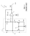
- this Figure 1 shows a generator 1 of a Band Gap voltage reference VBG.
- This generator 1 comprises an operational amplifier 2 inserted between a first and a second voltage reference, in particular a supply voltage reference VDD and a ground GND.
- the operational amplifier 2 has a first input terminal T1, in particular an inverting one (-), and a second input terminal T2, in particular a non inverting one (+), as well as an output terminal, corresponding to the output terminal OUT of the generator 1, where the Band Gap voltage reference VBG is supplied.
- the generator 1 also comprises a bipolar stage 3 inserted between the output terminal OUT of the operational amplifier 2 and the ground GND and comprising a first Q1 and a second bipolar transistor Q2, as well as a first R1, a second R2 and a third resistive element R3.
- the first bipolar transistor Q1 is inserted between the second input terminal T2 of the operational amplifier 2 and the ground GND and has a control or base terminal connected to the base terminal of the second bipolar transistor Q2 and both connected to ground (both the bipolar transistors are diode-connected).
- the bipolar transistor Q2 is also connected, through the first resistive element R1, to the first input terminal T1 of the operational amplifier 2 as well as to the ground GND.
- the second input terminal T2 of the operational amplifier 2 is also feedback connected to its output terminal OUT, by means of the second resistive element R2 and the first input terminal T1 of the operational amplifier 2 is similarly feedback connected to its output terminal OUT, by means of the third resistive element R3.
- the operational amplifier 2 performs the double function of realising a current proportional to the thermal voltage VT and of ensuring the output supply of a Band Gap voltage reference VBG with low impedance, which is desirable, when the generator 1 should supply current.
- V BG V EB ⁇ 1 + R 3 R 1 ⁇ V T ⁇ ln R 3 R 2 ⁇ k V EB1 being the voltage between the base and emitter terminals of the first bipolar transistor Q1 and R1, R2, R3 the resistive values of the first, second and third resistive elements.
- the minimum value of the supply voltage reference VDD of the generator 1 under examination depends on the effective physical realisation of the operational amplifier 2, but it results in any case limited below by the reference voltage value calculated for having a null variation at the environment temperature, equal to about 1.26V, as above indicated.
- the generator 1 realised by means of the operational amplifier 2 and shown in Figure 1 cannot thus be used in applications having supply voltages lower than about 1.3V.
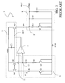
- the generator 5 also comprises an operational amplifier 2 having a first input terminal T1, in particular an inverting one (-), and a second input terminal T2, in particular a non inverting one (+), as well as an output terminal OUT.
- the generator 5 further comprises an input stage 6 inserted between the input terminals, T1 and T2, of the operational amplifier 2 and the ground GND, in turn including a first Q1 and a second bipolar transistor Q2, as well as a first R1, a second R2 and a third resistive element R3.
- the first bipolar transistor Q1 is inserted, in series with the first resistive element R1, between the first input terminal T1 of the operational amplifier 2 and the ground GND and has a control or base terminal connected to the ground GND.
- the second bipolar transistor Q2 is in turn inserted, in series with the second and the third resistive element R2, R3, between the second input terminal T2 of the operational amplifier 2 and the ground GND and has a control or base terminal connected to the ground GND.
- the generator 5 also comprises a current mirror 7, inserted between the supply voltage reference VDD and an inner circuit node X' and connected to the input terminals T1, T2 of the operational amplifier 2, as well as with its output terminal OUT and including a first, a second and a third MOS transistor, M 1, M2 and M3 as well as a first capacitor C1.
- the first MOS transistor M1 is inserted between the supply voltage reference VDD and the first input terminal T1 of the operational amplifier 2 and has a control or gate terminal connected to the control or gate terminal of the second MOS transistor M2, and both connected to the output terminal OUT of the operational amplifier, the second MOS transistor M2 being in turn inserted between the supply voltage reference VDD and the second input terminal T2 of the operational amplifier 2.
- the third MOS transistor M3 is inserted between the supply voltage reference VDD and the inner circuit node X' and has the control or gate terminal connected to the output terminal OUT of the operational amplifier 2 as well as with the bulk terminal of the second MOS transistor M2.
- the first capacitor C1 of the current mirror 7 is inserted between the supply voltage reference VDD and the output terminal OUT of the operational amplifier 2.
- the current mirror 7 is able to supply the inner circuit node X' with a value of current IP1 proportional to the current flowing in the first bipolar transistor Q1 of the input stage 6.
- the generator 5 also comprises an output stage 8 inserted between the inner circuit node X' and the ground GND and connected to the output terminal OUT' of the generator 5 and comprising a third bipolar transistor Q3, a fourth and a fifth resistive element R4 and R5 and a second capacitor C2.
- the fourth resistive element R4 and the third bipolar transistor Q3 are inserted, in series with each other, between the inner circuit node X' and the ground GND, the third bipolar transistor Q3 also having a control or base terminal in turn connected to the ground GND.
- the fifth resistive element R5 and the second capacitor C2 are inserted, in parallel to each other, between the inner circuit node X' and the ground GND.
- resistive elements R1 and R3 are suitable for ensuring that signals at the input of the operational amplifiers 2 are adequate also at high temperatures, when the voltage value between the base and emitter terminals V EB of the bipolar transistors is low.
- the differential pair with which the operational amplifier is realised should be of the n-channel type since a pair of p-channel transistors would be off for values of the supply voltage below about 1.4V.
- the resistive elements R1 and R3 put in series with the bipolar transistors Q1 and Q2 have exactly the function of allowing a correct operation range at the input terminals T1 and T2 of the operational amplifier 2, substantially increasing by a certain amount the voltage value at the input terminals T1 and T2 of the operational amplifier 2, since the voltage VBE of these bipolar transistors Q1 and Q2 at high temperatures decreases too much for ensuring the turn-on of the n-channel transistors.
- a generator 5 is obtained able to offer good performances down to values of the supply voltage equal to about 1.1V.
- the technical problem underlying the present invention is that of providing a generator circuit of a voltage reference independent from the temperature and having such structural and functional characteristics as to allow to overcome the limits and the drawbacks still affecting the generators realised according to the prior art and in particular, in the case of applications with low values of the supply voltage, to ensure that the voltage value applied to the input terminals of the operational amplifier contained in the Band Gap generator is enough to ensure the turn-on of its input n-channel pair.
- the solution idea underlying the present invention is that of suitably and dynamically driving the control terminals of bipolar transistors connected to the input terminals of the operational amplifier of the Band Gap generator contained in the generator circuit of a temperature-compensated voltage reference so as to maintain a voltage value applied across this operational amplifier as constant as possible when the temperature varies, thus obtaining a correct common mode voltage range applied to these input terminals and thus a correct operation of its input n-channel pair for very low values, in particular lower than 1V, of the supply voltage.
- the invention advantageously provides the generation of a base biasing voltage which depends on the temperature in an inverse way with respect to the base-emitter voltage of the bipolar transistors connected to the input terminals of the operational amplifier of the Band Gap circuit and is summed thereto to compensate its variations with the temperature and obtain at the input terminals of this operational amplifier a voltage having a suitable value in the whole temperature range.
- the problem is also solved by a method for generating a temperature-compensated voltage reference of the previously indicated type defined by the characterising part of claim 12.
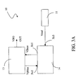
- a circuit generating a temperature-compensated voltage reference in particular using a Band Gap voltage, is schematically and globally indicated with 10, hereafter simply indicated as generator 10.
- the generator 10 essentially comprises a generator circuit 13 of a Band Gap voltage VBG, indicated as Band Gap circuit 13.
- the Band Gap circuit 13 essentially comprises an operational amplifier having at least one first and one second bipolar transistor connected to the input terminals of this operational amplifier and an output terminal OUT. It is also known that this operational amplifier comprises, connected to these input terminals, a pair of differential MOS n-channel transistors.
- the Band Gap circuit 13 is connected, in correspondence with a first and a second control node, Xc1 and Xc2, with a control block 14.
- the control block 14 is suitable for imposing, in correspondence with the first control node Xc1, a first biasing voltage value VBase on the base terminals of the bipolar transistors of the Band Gap circuit 13, in particular, such a voltage value that, added to the voltage value between the base and emitter terminals, V BE , of these bipolar transistors, an adequate common mode voltage is obtained being able to ensure the correct operation of the operational amplifier comprised in the Band Gap circuit 13 and in particular the turn-on of its differential pair of input n-channel MOS transistors.
- control block 14 receives, in correspondence with the second control node Xc2, a second biasing voltage value Vpbias.
- Vpbias a biasing voltage value having at least one component which increases with the temperature T to compensate the variations of the voltage between the base and emitter terminals V BE .
- an amount is deducted constant with the temperature T to add a fix base to the voltage value as obtained and thus suitably fix the common mode voltage level at the input terminals of the operational amplifier.
- the generator 10 also comprises a reference block 11 connected to a third control node Xc3 of the control block 14 and supplying it with a voltage value constant with the temperature, Viref.
- the reference block 11 generates a current value constant with the temperature, Iref, starting from the value of the Band Gap voltage VBG generated by the Band Gap circuit 13, which is mirrored through a reference voltage Viref.
- the reference block 11 is inserted between a first and a second voltage reference, in particular a supply voltage reference VDD and a ground GND and includes a current reference 12 in turn essentially including an operational amplifier OTA (transconductance amplifier).
- OTA transconductance amplifier
- the operational amplifier OTA has a first input terminal, in particular an inverting one (-), and a second input terminal, in particular a non inverting one (+) as well as an output terminal connected to a first inner circuit node X1.
- the second input terminal of the operational amplifier OTA is suitably connected to the output terminal OUT of the Band Gap circuit 13 and receives therefrom the Band Gap voltage VBG.
- the current reference 12 further comprises a first and a second MOS transistor, M1 and M2, and a first resistive element R1.
- the first MOS transistor M1 is inserted between the supply voltage reference VDD and the first input terminal of the operational amplifier OTA and has a control or gate terminal connected to the first inner circuit node X1, as well as to a control or gate terminal of the second MOS transistor M2, in turn inserted between the supply voltage reference VDD and a second inner circuit node X2.
- the first resistive element R1 is in turn connected between the first inner circuit node X1 and the ground GND.
- the reference block 11 comprises a third MOS transistor M3 inserted between the second inner circuit node X2 at the output of the current reference 12 and the ground GND and having a control or gate terminal diode-connected to the second inner circuit node X2.
- the third MOS transistor M3 realises a mirror of a reference current Iref which mirrors a reference current Iref flowing in the first resistive element R1 and converts it into the reference voltage value Viref, supplying it to the third control node Xc3 of the control block 14.
- this reference current Iref is obtained starting from the Band Gap voltage VBG on a resistance R1 and is thus stable in temperature.
- the first and second transistors M1 and M2 are PMOS transistors and the third transistor M3 is an NMOS transistor.
- the generator 10 according to the invention is shown in greater detail in Figure 4 and in particular the Band Gap circuit 13, controlled by the control block 14.
- the generator 10 thus comprises the Band Gap circuit 13 connected to the control block 14 in correspondence with the first and second control nodes, Xc1 and Xc2, as well as to the reference block 11 in correspondence with the third control node Xc3.
- the Band Gap circuit 13 comprises an operational amplifier OA1 having a first input terminal T1, in particular an inverting one (-) and a second input terminal T2, in particular a non inverting one (+), as well as an output terminal Tout.
- first and second input terminals, T1 and T2 are connected, as seen in relation with the prior art, to an input stage 15 comprising a first and a second bipolar transistor, Q1 and Q2, and a second resistive element R2.
- the first bipolar transistor Q1 is inserted between the second input terminal T2 of the operational amplifier OA1 and the ground GND and has a control or base terminal connected, in correspondence with the first control node Xc1, to the control or base terminal of the second bipolar transistor Q2.
- the second resistive element R2 and the second bipolar transistor Q2 are inserted, in series with each other, between the first input terminal T1 of the operational amplifier OA1 and the ground GND.
- the common base terminals of the first and second bipolar transistors, Q1 and Q2, of the input stage 15 are connected to the control block 14 and receive therefrom the first biasing voltage value VBase.
- the Band Gap circuit 13 comprises a current mirror 16 connected to the input and output terminals of the operational amplifier OA1 and comprising a first, a second, a third and a fourth mirror MOS transistor, MS1, MS2, MS3 and MS4.
- the first mirror MOS transistor MS1 is inserted between the supply voltage reference VDD and a third inner circuit node X3 and has a control or gate terminal connected to the output terminal Tout of the operational amplifier OA1 and to the control or gate terminal of the second mirror MOS transistor MS2, in turn inserted between the supply voltage reference VDD and the output terminal OUT of the Band Gap circuit 13, corresponding to the output terminal of the generator 10.
- the third and fourth mirror MOS transistors MS3 and MS4 are inserted between the supply voltage reference VDD and the second and first input terminals T2 and T1 of the operational amplifier OA1, respectively, and have respective control or gate terminal connected to each other and to the output terminal Tout of the operational amplifier OA1.
- the mirror transistors MS1, MS2, MS3 and MS4 are PMOS transistors.
- the Band Gap circuit 13 comprises an output stage 17 connected to the output terminal OUT.
- the output stage 17 comprises in turn a third bipolar transistor Q3 inserted between the third inner circuit node X3 and the ground GND and having the control or base terminal connected to the ground GND, as well as a resistive divider 18 including a first resistive element R1' connected between the third inner circuit node X3 and the output terminal OUT and a second resistive element R2' connected between the output terminal OUT and the ground GND.
- the output stage 17, and in particular the resistive divider 18, allows to fix the value of the Band Gap voltage VBG obtained at the output terminal OUT to the desired value, for example equal to 0.65V.
- the common base terminal of the bipolar transistors Q1 and Q2 is connected to the first control node Xc1 of the control block 14 suitable for imposing a first biasing voltage value VBase, in particular, such a voltage value that, added to the voltage value between the base and emitter terminals, V BE , of these bipolar transistors, an adequate common mode voltage is obtained being able to ensure the correct operation of the operational amplifier OA1, in particular suitable for ensuring the turn-on of the pair of input n-channel MOS transistors of this operational amplifier OA1.
- VBase a first biasing voltage value
- control block 14 is inserted between the supply voltage reference VDD and the ground GND and has an input terminal in correspondence with the third control node Xc3 and an output terminal in correspondence with the first control node Xc1.
- the control block 14 comprises a first and a second MOS transistor, M5 and M6, inserted, in series with each other, between the supply voltage reference VDD and the first control node Xc1 and interconnected in correspondence with a fourth inner circuit node X4, as well as a third and a fourth MOS transistor, M10 and M7, inserted, in series with each other, between the supply voltage reference VDD and a fifth inner circuit node X5.
- the first transistor M5 is a PMOS transistor and has a control or gate terminal connected, in correspondence with the terminal Tout, which is the output terminal of the operational amplifier OA1 of Figure 4 , with the control or gate terminal of the third transistor M10, also a PMOS transistor.
- the second transistor M6 is an NMOS transistor and has a control or gate terminal connected to the control or gate terminal of the fourth transistor M7, also an NMOS transistor and diode-connected.
- the control block 14 further comprises a fifth and a sixth MOS transistor, M8 and M9, inserted, in parallel to each other, between the first control node Xc1 and the ground GND.
- the fifth transistor M8 is an NMOS transistor and has a control or gate terminal connected to the fourth inner circuit node X4
- the sixth transistor M9 is an NMOS transistor and has a control or gate terminal connected to the third control node Xc3.
- the control block 14 also comprises a seventh MOS transistor M11 and a resistive element R3 inserted, in parallel to each other, between the fifth inner circuit node X5 and the ground GND.
- the seventh transistor M11 is an NMOS transistor having a control or gate terminal connected to the third control node Xc3.
- control block 14 receives on the third control node Xc3 a reference voltage value Viref supplied by the reference block 11.
- the control block 14 supplies to the first control node Xc 1 a first biasing voltage value VBase equal to the voltage value VSource being at the fifth inner circuit node X5 and equal to:
- a current Iptat flows equal to ⁇ Veb/R2, ⁇ Veb being the difference between the two base-emitter voltages Veb of the two bipolar transistors Q1 and Q2 of the input stage 15, which is divided into a first current proportional to the reference current Iref which flows in the branch comprising the seventh transistor M11 and a second current Ir which flows in the branch comprising the resistive element R3.
- a current flows proportional to the reference current Iref.
- the sizes of the seventh transistor M11 are chosen so as to be equal to n times those of the sixth transistor M9, n being a suitably chosen multiplicative parameter.
- Vcommon Veb + ⁇ Veb * R ⁇ 3 / R ⁇ 2 - n * VBG * R ⁇ 3 / R ⁇ 1 being
- Veb the voltage value between the emitter and base terminals of the first bipolar transistor Q1 of the input stage 15 and ⁇ Veb the difference between the two base-emitter voltages Veb of the two bipolar transistors Q1 and Q2 of the input stage 15;
- VBG the Band Gap voltage value supplied by the Band Gap circuit 13;
- R1 the resistive value of the resistive element of the reference block 11;
- R2 the resistive value of the resistive element connected to the second bipolar transistor Q2 in the input stage 15; and R3 the resistive value of the resistive element of the control block 14.
- control block 14 allows to obtain a resulting voltage given by a first component which decreases with the temperature T (Veb) and by a second component which increases with the temperature T ( ⁇ Veb*(R3/R2)), which compensates the variations of the first component, components from which a third component constant with the temperature T (n*VBG*(R3/R1)) is deducted.
- the third component allows to add a fix base to the voltage value obtained and thus to suitably fix the common mode level at the input terminals of the operational amplifier.
- FIG. 6 The overall scheme of the generator 10 according to the invention is shown in Figure 6 , where, by way of simplicity, the illustration of the reference block 11 has been omitted and where a sixth inner circuit node X6 has been further indicated corresponding to the common gate terminals of the transistors M6 and M7.
- the generator 10 then supplies a Band Gap voltage VBG reference sufficiently independent from the temperature and operating with supply voltages below 1V.
- the invention also relates to a method for generating a temperature-compensated voltage reference VBG starting from a Band Gap voltage obtained by a Band Gap circuit 13 comprising an operational amplifier OA1 having the input terminals connected to at least one first and one second bipolar transistor, Q1 and Q2.
- the method thus comprises the steps of:
- the driving step provides that the control block 14 imposes to the base terminal of the first bipolar transistor Q1 a biasing voltage value VBase comprising at least one voltage component which increases with the temperature ( ⁇ Veb*(R3/R2) to compensate the variations of the voltage (VBE) inversely proportional to the temperature obtained between the base and emitter terminals VBE of the first bipolar transistor Q1.
- VBase biasing voltage value
- VBE voltage component which increases with the temperature ( ⁇ Veb*(R3/R2) to compensate the variations of the voltage (VBE) inversely proportional to the temperature obtained between the base and emitter terminals VBE of the first bipolar transistor Q1.
- the driving step of the base terminal of the first bipolar transistor Q1 further generates a third subtractive component of the biasing voltage value constant with the temperature (n*VBG*(R3/R1) and able to add a fix base to the voltage value obtained and thus a degree of freedom for the fixing of the common mode value at the input terminals of the operational amplifier.
- the proposed generator 10 finds particular application in the memories for Smart Cards and the invention also relates to a memory for Smart card of the type comprising at least one generator 10 of a temperature-compensated voltage reference as above described.
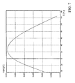
- Figure 7 shows an analysis in temperature of the generator 10 according to the invention simulated with a supply voltage equal to 0.9V and making the temperature vary from -40 °C to 125 °C.
- the global variation of the Band Gap voltage VBG in the whole temperature range as considered is lower than 3mV.
- Figure 8 reports a rejection analysis on the supply or PSRR (Power Supply Rejection Ratio) of the generator 10 carried out with a supply voltage equal to 0.9V. It then occurs that the generator 10 according to the invention ensures a PSRR value of about 65 dB at low frequencies and a worse case of about 31 dB at a frequency of 50 kHz.
- PSRR Power Supply Rejection Ratio
- the generator 10 according to the invention has the following advantages:
- the proposed implementation of the circuit according to the invention also takes into due consideration the area occupation, parameter that becomes more and more important when the technology evolves.
Landscapes
- Engineering & Computer Science (AREA)
- Microelectronics & Electronic Packaging (AREA)
- Physics & Mathematics (AREA)
- Power Engineering (AREA)
- Nonlinear Science (AREA)
- Electromagnetism (AREA)
- General Physics & Mathematics (AREA)
- Radar, Positioning & Navigation (AREA)
- Automation & Control Theory (AREA)
- Control Of Electrical Variables (AREA)
- Amplifiers (AREA)
Abstract
Description
- The present invention relates to a circuit for generating a temperature-compensated voltage reference.
- More specifically, the invention relates to a circuit of the type comprising at least one current reference, inserted between a first and a second voltage reference and including an operational amplifier, having in turn a first and a second input terminal connected to an input stage essentially comprising a generator circuit of a current proportional to the temperature by means of at least one first bipolar transistor, as well as a current mirror connected to the first supply voltage reference and inserted between the first and the second input terminal of the operational amplifier and an output terminal of the circuit suitable for supplying this temperature-compensated voltage reference.
- The invention particularly, but not exclusively, relates to a generator circuit of a voltage of the Band Gap type and the following description is made with reference to this field of application by way of illustration only.
- As it is well known, the circuits for the generation of a voltage reference, also simply indicated as voltage references, are widely used in the integrated circuits for the most varied needs.
- These circuits supply, in particular, at least one electric quantity having a high accuracy and stability that can be used in general as reference in several circuit blocks, such as for example, analogue/digital converters, voltage regulators, detection and/or measurement circuits, etc.
- A voltage reference should thus be strong for the applications it is intended for and in particular be characterised by a good thermal stability and by a good noise rejection, so as to supply a constant output voltage value independent from the variations of the supply voltage and of the working temperature of the integrated circuit comprising it.
- To this purpose, circuits are commonly used generating a voltage reference of the Band Gap type, or more simply Band Gap generators, wherein, essentially, the potential jump of the silicon prohibited band (about 1.1 eV) is exploited for generating an accurate voltage reference independent from the working temperature.
- In particular, such a Band Gap generator arises from the realisation that a voltage VBG almost independent from the working temperature can be obtained in a simple way by means of a bipolar transistor by implementing the following equation:

- In fact, as it is well known, the voltage VBE between base and emitter of a bipolar transistor decreases when the temperature increases (∼-2.2mV/°C @ T=300°K), while the thermal voltage VT is proportional to the temperature itself. In other words, a voltage (VBE) is to be compensated which decreases with the absolute temperature, i.e. it is CTAT (Complementary To Absolute Temperature) with a corrective coefficient (nVT) which is proportional to the absolute temperature or PTAT (Proportional To Absolute Temperature).
- To obtain a voltage reference independent from the temperature it is necessary to determine the value of the parameter n for which the derivative of the Band Gap voltage VBG, with respect to the temperature, is equal to zero considering a temperature T=T* equal to a desired working temperature. For example if a null variation of the Band Gap voltage reference VBG is to be obtained at the temperature of 27°C, a value of about 1.26V for VBG is found, the voltage VBE being at environment temperature equal to about 0.6V and the parameter n equal to about 26.
- It is also known that a Band Gap generator can be realised in full CMOS technology realising the bipolar transistors by means of parasite diodes. A possible implementation using an operational amplifier is shown in
Figure 1 . - In particular, this
Figure 1 shows agenerator 1 of a Band Gap voltage reference VBG. Thisgenerator 1 comprises anoperational amplifier 2 inserted between a first and a second voltage reference, in particular a supply voltage reference VDD and a ground GND. - The
operational amplifier 2 has a first input terminal T1, in particular an inverting one (-), and a second input terminal T2, in particular a non inverting one (+), as well as an output terminal, corresponding to the output terminal OUT of thegenerator 1, where the Band Gap voltage reference VBG is supplied. - The
generator 1 also comprises abipolar stage 3 inserted between the output terminal OUT of theoperational amplifier 2 and the ground GND and comprising a first Q1 and a second bipolar transistor Q2, as well as a first R1, a second R2 and a third resistive element R3. - More in particular, the first bipolar transistor Q1 is inserted between the second input terminal T2 of the
operational amplifier 2 and the ground GND and has a control or base terminal connected to the base terminal of the second bipolar transistor Q2 and both connected to ground (both the bipolar transistors are diode-connected). The bipolar transistor Q2 is also connected, through the first resistive element R1, to the first input terminal T1 of theoperational amplifier 2 as well as to the ground GND. - The second input terminal T2 of the
operational amplifier 2 is also feedback connected to its output terminal OUT, by means of the second resistive element R2 and the first input terminal T1 of theoperational amplifier 2 is similarly feedback connected to its output terminal OUT, by means of the third resistive element R3. - It is to be noted that the
operational amplifier 2 performs the double function of realising a current proportional to the thermal voltage VT and of ensuring the output supply of a Band Gap voltage reference VBG with low impedance, which is desirable, when thegenerator 1 should supply current. - Thanks to the presence of the
operational amplifier 2 it is possible to assume that the voltage values on its input terminals T1 and T2 are identical (V+=V-), by putting AE2=kAE1, AE2, AE1 being the areas of the emitter terminals of the first and second bipolar transistors Q1 and Q2, respectively and k being a suitable project parameter calculated to obtain the desired temperature compensation. - Observing moreover that R2*IC1=R3*IC2, R2 and R3 being the resistive values of the second and third resistive elements R2 and R3, respectively, and IC1, IC2 the collector currents of the first and second bipolar transistors Q1 and Q2, respectively, the following is obtained:

- Wherefrom the expression of the Band Gap voltage reference VBG is easily derived:

- It is to be noted that the minimum value of the supply voltage reference VDD of the
generator 1 under examination depends on the effective physical realisation of theoperational amplifier 2, but it results in any case limited below by the reference voltage value calculated for having a null variation at the environment temperature, equal to about 1.26V, as above indicated. - The
generator 1 realised by means of theoperational amplifier 2 and shown inFigure 1 cannot thus be used in applications having supply voltages lower than about 1.3V. - It is also possible to modify the
generator 1 to adapt it to applications with supply voltage lower than 1.3V and to obtain thegenerator 5 shown inFigure 2 , also inserted between a first and a second voltage reference, in particular a supply voltage reference VDD and a ground GND and having an output terminal OUT' where the Band Gap voltage reference VBG is supplied. - The
generator 5 also comprises anoperational amplifier 2 having a first input terminal T1, in particular an inverting one (-), and a second input terminal T2, in particular a non inverting one (+), as well as an output terminal OUT. - The
generator 5 further comprises aninput stage 6 inserted between the input terminals, T1 and T2, of theoperational amplifier 2 and the ground GND, in turn including a first Q1 and a second bipolar transistor Q2, as well as a first R1, a second R2 and a third resistive element R3. - More in particular, the first bipolar transistor Q1 is inserted, in series with the first resistive element R1, between the first input terminal T1 of the
operational amplifier 2 and the ground GND and has a control or base terminal connected to the ground GND. - Similarly, the second bipolar transistor Q2 is in turn inserted, in series with the second and the third resistive element R2, R3, between the second input terminal T2 of the
operational amplifier 2 and the ground GND and has a control or base terminal connected to the ground GND. - The
generator 5 also comprises acurrent mirror 7, inserted between the supply voltage reference VDD and an inner circuit node X' and connected to the input terminals T1, T2 of theoperational amplifier 2, as well as with its output terminal OUT and including a first, a second and a third MOS transistor,M 1, M2 and M3 as well as a first capacitor C1. - More in particular, the first MOS transistor M1 is inserted between the supply voltage reference VDD and the first input terminal T1 of the
operational amplifier 2 and has a control or gate terminal connected to the control or gate terminal of the second MOS transistor M2, and both connected to the output terminal OUT of the operational amplifier, the second MOS transistor M2 being in turn inserted between the supply voltage reference VDD and the second input terminal T2 of theoperational amplifier 2. Similarly the third MOS transistor M3 is inserted between the supply voltage reference VDD and the inner circuit node X' and has the control or gate terminal connected to the output terminal OUT of theoperational amplifier 2 as well as with the bulk terminal of the second MOS transistor M2. - Finally, the first capacitor C1 of the
current mirror 7 is inserted between the supply voltage reference VDD and the output terminal OUT of theoperational amplifier 2. - In this way, the
current mirror 7 is able to supply the inner circuit node X' with a value of current IP1 proportional to the current flowing in the first bipolar transistor Q1 of theinput stage 6. - The
generator 5 also comprises anoutput stage 8 inserted between the inner circuit node X' and the ground GND and connected to the output terminal OUT' of thegenerator 5 and comprising a third bipolar transistor Q3, a fourth and a fifth resistive element R4 and R5 and a second capacitor C2. - More in particular, the fourth resistive element R4 and the third bipolar transistor Q3 are inserted, in series with each other, between the inner circuit node X' and the ground GND, the third bipolar transistor Q3 also having a control or base terminal in turn connected to the ground GND. Similarly, the fifth resistive element R5 and the second capacitor C2 are inserted, in parallel to each other, between the inner circuit node X' and the ground GND.
- It is to be noted that the voltage values on the input terminals T1 and T2 of the
operational amplifier 2 being equal (V+=V-) and having:
- AE2, AE1 the areas of the emitter terminals of the first and second bipolar transistors Q1 and Q2, respectively, of the
input stage 6 and n a suitable multiplicative coefficient calculated to obtain the desired compensation in temperature, - R1, R3 the resistance values of the first and of the second resistive element of the
input stage 6, and - IP, IP1 the current values flowing in the first bipolar transistor Q1 of the
input stage 6 and in correspondence with the inner circuit node X' at the output of thecurrent mirror 7, respectively, and k1 a suitable multiplicative coefficient introduced by the dimensional ratio of thetransistors M 1 and M3 of thiscurrent mirror 7
with simple mathematical passages, it is possible to obtain the following expression of the Band Gap voltage reference VBG:
- R2 the resistance value of the second resistive element of the
input stage 6, - R4, R5 the resistance values of the fourth and fifth resistive elements of the
output stage 8, - VEB3 the voltage value between the base and emitter terminals of the third bipolar transistor Q3 of the
output stage 8; and - IS1, IS2 the inverse saturation current values of the first and second bipolar transistors Q1 and Q2, respectively.
- R2 the resistance value of the second resistive element of the
- It thus occurs that the resistive elements R1 and R3 are suitable for ensuring that signals at the input of the
operational amplifiers 2 are adequate also at high temperatures, when the voltage value between the base and emitter terminals VEB of the bipolar transistors is low. - In fact, it is to be noted that the differential pair with which the operational amplifier is realised (not shown in the figure), for applications with low supply voltage values, should be of the n-channel type since a pair of p-channel transistors would be off for values of the supply voltage below about 1.4V. The resistive elements R1 and R3 put in series with the bipolar transistors Q1 and Q2 have exactly the function of allowing a correct operation range at the input terminals T1 and T2 of the
operational amplifier 2, substantially increasing by a certain amount the voltage value at the input terminals T1 and T2 of theoperational amplifier 2, since the voltage VBE of these bipolar transistors Q1 and Q2 at high temperatures decreases too much for ensuring the turn-on of the n-channel transistors. - In this way, a
generator 5 is obtained able to offer good performances down to values of the supply voltage equal to about 1.1V. - However, for lower supply voltage values, and especially at low temperatures, when the voltage value between the base and emitter terminals VEB of the bipolar transistors is high, it immediately occurs that the first and the second MOS transistors M1 and M2 of the
current mirror 7 operate with a very low voltage value between the source and drain terminals Vds, and in particular quite different from the voltage value between the source and drain terminals Vds of the third MOS transistor M3, this latter voltage being considered constant for the whole temperature range. - These different operative conditions cause mirroring errors of the currents, which result in a bad behaviour of the
generator 5 when the temperature varies. - The technical problem underlying the present invention is that of providing a generator circuit of a voltage reference independent from the temperature and having such structural and functional characteristics as to allow to overcome the limits and the drawbacks still affecting the generators realised according to the prior art and in particular, in the case of applications with low values of the supply voltage, to ensure that the voltage value applied to the input terminals of the operational amplifier contained in the Band Gap generator is enough to ensure the turn-on of its input n-channel pair.
- The solution idea underlying the present invention is that of suitably and dynamically driving the control terminals of bipolar transistors connected to the input terminals of the operational amplifier of the Band Gap generator contained in the generator circuit of a temperature-compensated voltage reference so as to maintain a voltage value applied across this operational amplifier as constant as possible when the temperature varies, thus obtaining a correct common mode voltage range applied to these input terminals and thus a correct operation of its input n-channel pair for very low values, in particular lower than 1V, of the supply voltage.
- More in particular, the invention advantageously provides the generation of a base biasing voltage which depends on the temperature in an inverse way with respect to the base-emitter voltage of the bipolar transistors connected to the input terminals of the operational amplifier of the Band Gap circuit and is summed thereto to compensate its variations with the temperature and obtain at the input terminals of this operational amplifier a voltage having a suitable value in the whole temperature range.
- On the basis of this solution idea the technical problem is solved by a generator circuit of a temperature-compensated voltage reference of the previously indicated type defined by the characterising part of
claim 1. - The problem is also solved by a method for generating a temperature-compensated voltage reference of the previously indicated type defined by the characterising part of
claim 12. - The characteristics and advantages of the circuit and of the method according to the invention will be apparent from the following description given by way of indicative and non limiting example with reference to the annexed drawings.
- In these drawings:
-
Figure 1 schematically shows a possible circuit implementation of a generation circuit of a Band Gap voltage reference realised according to the prior art; -
Figure 2 schematically shows a further embodiment of a generator circuit of a Band Gap voltage reference realised according to the prior art and suitable for applications with low supply voltages; -
Figure 3A schematically shows a circuit for generating a temperature compensated voltage reference realised according to the invention; -
Figure 3B schematically but in further detail shows the circuit ofFigure 3A ; -
Figure 4 schematically and in further detail shows the circuit ofFigure 3A ; -
Figure 5 schematically shows a detail of the circuit ofFigure 3A ; -
Figure 6 schematically shows a possible circuit implementation of the generator circuit of a temperature-compensated voltage reference according to the invention; and -
Figure 7 shows the pattern of the temperature-compensated voltage reference obtained by the generation circuit according to the invention when the temperature varies; -
Figure 8 shows the rejection analysis on the supply or PSRR (Power Supply Rejection Ratio) of the generation circuit according to the invention carried out with a supply voltage equal to 0.9V. - With reference to these figures, and in particular to
Figure 3A , a circuit generating a temperature-compensated voltage reference, in particular using a Band Gap voltage, is schematically and globally indicated with 10, hereafter simply indicated asgenerator 10. - The
generator 10 essentially comprises agenerator circuit 13 of a Band Gap voltage VBG, indicated asBand Gap circuit 13. As seen in relation to the prior art, theBand Gap circuit 13 essentially comprises an operational amplifier having at least one first and one second bipolar transistor connected to the input terminals of this operational amplifier and an output terminal OUT. It is also known that this operational amplifier comprises, connected to these input terminals, a pair of differential MOS n-channel transistors. - Advantageously according to the invention, the
Band Gap circuit 13 is connected, in correspondence with a first and a second control node, Xc1 and Xc2, with acontrol block 14. In particular, thecontrol block 14 is suitable for imposing, in correspondence with the first control node Xc1, a first biasing voltage value VBase on the base terminals of the bipolar transistors of theBand Gap circuit 13, in particular, such a voltage value that, added to the voltage value between the base and emitter terminals, VBE, of these bipolar transistors, an adequate common mode voltage is obtained being able to ensure the correct operation of the operational amplifier comprised in theBand Gap circuit 13 and in particular the turn-on of its differential pair of input n-channel MOS transistors. Moreover, thecontrol block 14 receives, in correspondence with the second control node Xc2, a second biasing voltage value Vpbias. As it will be clear hereafter in the description, advantageously according to the invention, thecontrol block 14 imposes a biasing voltage value having at least one component which increases with the temperature T to compensate the variations of the voltage between the base and emitter terminals VBE. Moreover, advantageously according to the invention, from the sum of these voltages, an amount is deducted constant with the temperature T to add a fix base to the voltage value as obtained and thus suitably fix the common mode voltage level at the input terminals of the operational amplifier. - Advantageously according to the invention, the
generator 10 also comprises areference block 11 connected to a third control node Xc3 of thecontrol block 14 and supplying it with a voltage value constant with the temperature, Viref. - In a preferred embodiment of the invention, the
reference block 11 generates a current value constant with the temperature, Iref, starting from the value of the Band Gap voltage VBG generated by theBand Gap circuit 13, which is mirrored through a reference voltage Viref. - In this case, as schematically shown in
Figure 3B , thereference block 11 is inserted between a first and a second voltage reference, in particular a supply voltage reference VDD and a ground GND and includes acurrent reference 12 in turn essentially including an operational amplifier OTA (transconductance amplifier). - The operational amplifier OTA has a first input terminal, in particular an inverting one (-), and a second input terminal, in particular a non inverting one (+) as well as an output terminal connected to a first inner circuit node X1. The second input terminal of the operational amplifier OTA is suitably connected to the output terminal OUT of the
Band Gap circuit 13 and receives therefrom the Band Gap voltage VBG. - In particular, the
current reference 12 further comprises a first and a second MOS transistor, M1 and M2, and a first resistive element R1. The first MOS transistor M1 is inserted between the supply voltage reference VDD and the first input terminal of the operational amplifier OTA and has a control or gate terminal connected to the first inner circuit node X1, as well as to a control or gate terminal of the second MOS transistor M2, in turn inserted between the supply voltage reference VDD and a second inner circuit node X2. The first resistive element R1 is in turn connected between the first inner circuit node X1 and the ground GND. - Moreover, the
reference block 11 comprises a third MOS transistor M3 inserted between the second inner circuit node X2 at the output of thecurrent reference 12 and the ground GND and having a control or gate terminal diode-connected to the second inner circuit node X2. In this way, the third MOS transistor M3 realises a mirror of a reference current Iref which mirrors a reference current Iref flowing in the first resistive element R1 and converts it into the reference voltage value Viref, supplying it to the third control node Xc3 of thecontrol block 14. - It is to be noted that this reference current Iref is obtained starting from the Band Gap voltage VBG on a resistance R1 and is thus stable in temperature.
- In the embodiment shown in
Figure 3B , the first and second transistors M1 and M2 are PMOS transistors and the third transistor M3 is an NMOS transistor. - The
generator 10 according to the invention is shown in greater detail inFigure 4 and in particular theBand Gap circuit 13, controlled by thecontrol block 14. - As previously seen, the
generator 10 thus comprises theBand Gap circuit 13 connected to thecontrol block 14 in correspondence with the first and second control nodes, Xc1 and Xc2, as well as to thereference block 11 in correspondence with the third control node Xc3. - The
Band Gap circuit 13 comprises an operational amplifier OA1 having a first input terminal T1, in particular an inverting one (-) and a second input terminal T2, in particular a non inverting one (+), as well as an output terminal Tout. - More in particular, the first and second input terminals, T1 and T2, are connected, as seen in relation with the prior art, to an
input stage 15 comprising a first and a second bipolar transistor, Q1 and Q2, and a second resistive element R2. The first bipolar transistor Q1 is inserted between the second input terminal T2 of the operational amplifier OA1 and the ground GND and has a control or base terminal connected, in correspondence with the first control node Xc1, to the control or base terminal of the second bipolar transistor Q2. Moreover, the second resistive element R2 and the second bipolar transistor Q2 are inserted, in series with each other, between the first input terminal T1 of the operational amplifier OA1 and the ground GND. - Advantageously according to the invention, the common base terminals of the first and second bipolar transistors, Q1 and Q2, of the
input stage 15 are connected to thecontrol block 14 and receive therefrom the first biasing voltage value VBase. - Further, the
Band Gap circuit 13 comprises acurrent mirror 16 connected to the input and output terminals of the operational amplifier OA1 and comprising a first, a second, a third and a fourth mirror MOS transistor, MS1, MS2, MS3 and MS4. - In particular, the first mirror MOS transistor MS1 is inserted between the supply voltage reference VDD and a third inner circuit node X3 and has a control or gate terminal connected to the output terminal Tout of the operational amplifier OA1 and to the control or gate terminal of the second mirror MOS transistor MS2, in turn inserted between the supply voltage reference VDD and the output terminal OUT of the
Band Gap circuit 13, corresponding to the output terminal of thegenerator 10. Similarly, the third and fourth mirror MOS transistors MS3 and MS4 are inserted between the supply voltage reference VDD and the second and first input terminals T2 and T1 of the operational amplifier OA1, respectively, and have respective control or gate terminal connected to each other and to the output terminal Tout of the operational amplifier OA1. In the embodiment shown inFigure 4 , the mirror transistors MS1, MS2, MS3 and MS4 are PMOS transistors. - Moreover, the
Band Gap circuit 13 comprises anoutput stage 17 connected to the output terminal OUT. In particular, theoutput stage 17 comprises in turn a third bipolar transistor Q3 inserted between the third inner circuit node X3 and the ground GND and having the control or base terminal connected to the ground GND, as well as aresistive divider 18 including a first resistive element R1' connected between the third inner circuit node X3 and the output terminal OUT and a second resistive element R2' connected between the output terminal OUT and the ground GND. - It is to be underlined that the
output stage 17, and in particular theresistive divider 18, allows to fix the value of the Band Gap voltage VBG obtained at the output terminal OUT to the desired value, for example equal to 0.65V. - It is obviously possible to consider other configurations for the
output stage 17, in particular with the third bipolar transistor Q3 inserted in series with the first resistive element R1' between the output terminal OUT and the ground GND, in parallel with the second resistive element R2'. - As previously said, advantageously according to the invention, the common base terminal of the bipolar transistors Q1 and Q2 is connected to the first control node Xc1 of the
control block 14 suitable for imposing a first biasing voltage value VBase, in particular, such a voltage value that, added to the voltage value between the base and emitter terminals, VBE, of these bipolar transistors, an adequate common mode voltage is obtained being able to ensure the correct operation of the operational amplifier OA1, in particular suitable for ensuring the turn-on of the pair of input n-channel MOS transistors of this operational amplifier OA1. - It is in fact to be remembered that the common mode voltage applied to the input terminals of the operational amplifier OA1 should differ as little as possible with respect to the Band Gap output voltage VBG for consequently reducing the systematic error introduced by the
current mirror 16, in particular comprising MOS transistors of the P type, due to the so called Early effect. - This nullifying effect of the current mirror is obtained, advantageously according to the invention, by the
control block 14 shown in greater detail inFigure 5 . - In particular, the
control block 14 is inserted between the supply voltage reference VDD and the ground GND and has an input terminal in correspondence with the third control node Xc3 and an output terminal in correspondence with the first control node Xc1. - The
control block 14 comprises a first and a second MOS transistor, M5 and M6, inserted, in series with each other, between the supply voltage reference VDD and the first control node Xc1 and interconnected in correspondence with a fourth inner circuit node X4, as well as a third and a fourth MOS transistor, M10 and M7, inserted, in series with each other, between the supply voltage reference VDD and a fifth inner circuit node X5. - More in particular, the first transistor M5 is a PMOS transistor and has a control or gate terminal connected, in correspondence with the terminal Tout, which is the output terminal of the operational amplifier OA1 of
Figure 4 , with the control or gate terminal of the third transistor M10, also a PMOS transistor. Moreover, the second transistor M6 is an NMOS transistor and has a control or gate terminal connected to the control or gate terminal of the fourth transistor M7, also an NMOS transistor and diode-connected. - The
control block 14 further comprises a fifth and a sixth MOS transistor, M8 and M9, inserted, in parallel to each other, between the first control node Xc1 and the ground GND. In particular, the fifth transistor M8 is an NMOS transistor and has a control or gate terminal connected to the fourth inner circuit node X4, while the sixth transistor M9 is an NMOS transistor and has a control or gate terminal connected to the third control node Xc3. - The
control block 14 also comprises a seventh MOS transistor M11 and a resistive element R3 inserted, in parallel to each other, between the fifth inner circuit node X5 and the ground GND. In particular, the seventh transistor M11 is an NMOS transistor having a control or gate terminal connected to the third control node Xc3. - As previously seen, the
control block 14 receives on the third control node Xc3 a reference voltage value Viref supplied by thereference block 11. - Advantageously according to the invention, the
control block 14 supplies to the first control node Xc 1 a first biasing voltage value VBase equal to the voltage value VSource being at the fifth inner circuit node X5 and equal to:
- In fact, it is immediate to verify that, in the branch comprising the transistors M7 and M10, a current Iptat flows equal to ΔVeb/R2, ΔVeb being the difference between the two base-emitter voltages Veb of the two bipolar transistors Q1 and Q2 of the
input stage 15, which is divided into a first current proportional to the reference current Iref which flows in the branch comprising the seventh transistor M11 and a second current Ir which flows in the branch comprising the resistive element R3. Moreover, also in the branch comprising the sixth transistor M9 a current flows proportional to the reference current Iref. The value of the first current Iref is obtained by thereference block 11 starting from the Band Gap voltage VBG and is equal to Iref = VBG/R1, R1 being the resistive element of thecurrent reference 12 shown inFigure 3B . - Advantageously, the sizes of the seventh transistor M11 are chosen so as to be equal to n times those of the sixth transistor M9, n being a suitably chosen multiplicative parameter.
- In this way, the common mode voltage Vcommon applied to the input terminals T1 and T2 of the
operational amplifier 12 is given by
- Veb the voltage value between the emitter and base terminals of the first bipolar transistor Q1 of the
input stage 15 and ΔVeb the difference between the two base-emitter voltages Veb of the two bipolar transistors Q1 and Q2 of theinput stage 15;
VBG the Band Gap voltage value supplied by theBand Gap circuit 13;
R1 the resistive value of the resistive element of thereference block 11;
R2 the resistive value of the resistive element connected to the second bipolar transistor Q2 in theinput stage 15; and
R3 the resistive value of the resistive element of thecontrol block 14. - In other words, advantageously according to the invention, the
control block 14 allows to obtain a resulting voltage given by a first component which decreases with the temperature T (Veb) and by a second component which increases with the temperature T (ΔVeb*(R3/R2)), which compensates the variations of the first component, components from which a third component constant with the temperature T (n*VBG*(R3/R1)) is deducted. In particular, the third component allows to add a fix base to the voltage value obtained and thus to suitably fix the common mode level at the input terminals of the operational amplifier. - The overall scheme of the
generator 10 according to the invention is shown inFigure 6 , where, by way of simplicity, the illustration of thereference block 11 has been omitted and where a sixth inner circuit node X6 has been further indicated corresponding to the common gate terminals of the transistors M6 and M7. - Advantageously according to the invention, as above explained, the
generator 10 then supplies a Band Gap voltage VBG reference sufficiently independent from the temperature and operating with supply voltages below 1V. - The invention also relates to a method for generating a temperature-compensated voltage reference VBG starting from a Band Gap voltage obtained by a
Band Gap circuit 13 comprising an operational amplifier OA1 having the input terminals connected to at least one first and one second bipolar transistor, Q1 and Q2. - The method thus comprises the steps of:
- generating a first component of the temperature-compensated voltage reference which decreases with the temperature, as base-emitter voltage of one of said bipolar transistors, in particular of the first bipolar transistor Q1;
- driving the base terminal of the first bipolar transistor Q1 by applying the biasing voltage value VBase supplied by the
control block 14 connected to this base terminal; and - obtaining the temperature-compensated voltage value VBG on the output terminal OUT of the
generator 10. - Suitably, the driving step provides that the
control block 14 imposes to the base terminal of the first bipolar transistor Q1 a biasing voltage value VBase comprising at least one voltage component which increases with the temperature (ΔVeb*(R3/R2) to compensate the variations of the voltage (VBE) inversely proportional to the temperature obtained between the base and emitter terminals VBE of the first bipolar transistor Q1. In this way, as previously explained, the turn-on of the pair of n-channel input transistors of the operational amplifier OA1 is ensured. - Advantageously according to the invention, the driving step of the base terminal of the first bipolar transistor Q1 further generates a third subtractive component of the biasing voltage value constant with the temperature (n*VBG*(R3/R1) and able to add a fix base to the voltage value obtained and thus a degree of freedom for the fixing of the common mode value at the input terminals of the operational amplifier.
- The proposed
generator 10 finds particular application in the memories for Smart Cards and the invention also relates to a memory for Smart card of the type comprising at least onegenerator 10 of a temperature-compensated voltage reference as above described. - The results of experimental tests carried out by the Applicant are shown in
Figures 7 and8 . - In particular,
Figure 7 shows an analysis in temperature of thegenerator 10 according to the invention simulated with a supply voltage equal to 0.9V and making the temperature vary from -40 °C to 125 °C. - As it can be noted, the global variation of the Band Gap voltage VBG in the whole temperature range as considered is lower than 3mV.
-
Figure 8 reports a rejection analysis on the supply or PSRR (Power Supply Rejection Ratio) of thegenerator 10 carried out with a supply voltage equal to 0.9V. It then occurs that thegenerator 10 according to the invention ensures a PSRR value of about 65 dB at low frequencies and a worse case of about 31 dB at a frequency of 50 kHz. - In conclusion, the
generator 10 according to the invention has the following advantages: - ensures a correct operation of the current reference also with supply voltages lower than 1V;
- ensures a high rejection to the noise at the supply reference;
- has good performances in terms of sensitivity to the variation of the supply voltage and of the temperature; and
- offers a good compensation in temperature of the voltage value as obtained.
- Suitably, the proposed implementation of the circuit according to the invention also takes into due consideration the area occupation, parameter that becomes more and more important when the technology evolves.
Claims (15)
said first transistor (M5) having a control terminal connected to a control terminal of said third transistor (M10) and said second transistor (M6) having a control terminal connected to a control terminal of said fourth transistor (M7), in turn diode-connected, said common control terminals of said first and third transistors (M5, M10) being connected to the output terminal (Tout) of said operational amplifier (OA1).
said driving step providing that said control block (14) imposes to said base terminal of said first bipolar transistor (Q1) a biasing voltage value (VBase) comprising at least said voltage component which increases with the temperature for compensating the variations of said first voltage component (VBE) proportional to the temperature obtained between the base and emitter terminals (VBE) of said first bipolar transistor (Q1) and ensure the turn-on of a pair of input transistors of said operational amplifier (OA1).
Priority Applications (3)
| Application Number | Priority Date | Filing Date | Title |
|---|---|---|---|
| EP08425331.9A EP2120124B1 (en) | 2008-05-13 | 2008-05-13 | Circuit for generating a temperature-compensated voltage reference, in particular for applications with supply voltages lower than 1V |
| US12/464,481 US8120415B2 (en) | 2008-05-13 | 2009-05-12 | Circuit for generating a temperature-compensated voltage reference, in particular for applications with supply voltages lower than 1V |
| CN200910140925.5A CN101615050B (en) | 2008-05-13 | 2009-05-13 | Circuit for generating a temperature-compensated voltage reference, in particular for applications with supply voltages lower than 1V |
Applications Claiming Priority (1)
| Application Number | Priority Date | Filing Date | Title |
|---|---|---|---|
| EP08425331.9A EP2120124B1 (en) | 2008-05-13 | 2008-05-13 | Circuit for generating a temperature-compensated voltage reference, in particular for applications with supply voltages lower than 1V |
Publications (2)
| Publication Number | Publication Date |
|---|---|
| EP2120124A1 true EP2120124A1 (en) | 2009-11-18 |
| EP2120124B1 EP2120124B1 (en) | 2014-07-09 |
Family
ID=39925062
Family Applications (1)
| Application Number | Title | Priority Date | Filing Date |
|---|---|---|---|
| EP08425331.9A Active EP2120124B1 (en) | 2008-05-13 | 2008-05-13 | Circuit for generating a temperature-compensated voltage reference, in particular for applications with supply voltages lower than 1V |
Country Status (3)
| Country | Link |
|---|---|
| US (1) | US8120415B2 (en) |
| EP (1) | EP2120124B1 (en) |
| CN (1) | CN101615050B (en) |
Cited By (6)
| Publication number | Priority date | Publication date | Assignee | Title |
|---|---|---|---|---|
| WO2018015791A1 (en) * | 2016-07-22 | 2018-01-25 | CSEM Centre Suisse d'Electronique et de Microtechnique SA - Recherche et Développement | Compensation device for compensating pvt variations of an analog and/or digital circuit |
| CN108376010A (en) * | 2018-01-30 | 2018-08-07 | 深圳市明柏集成电路有限公司 | A kind of low temp rising high precision current source suitable for arbitrary resistance type |
| CN110377094A (en) * | 2019-05-17 | 2019-10-25 | 东南大学 | A kind of Low Drift Temperature extremely low power dissipation linear voltage regulator |
| CN112393814A (en) * | 2020-10-27 | 2021-02-23 | 北京智芯微电子科技有限公司 | Wide-range temperature calculation method and system, temperature sensor and temperature measurement method |
| CN113741613A (en) * | 2021-09-26 | 2021-12-03 | 电子科技大学 | Zero-temperature-adjustable ACOT charging current circuit |
| CN114356019A (en) * | 2022-01-04 | 2022-04-15 | 电子科技大学 | A Low Mismatch High Precision Voltage Reference Source |
Families Citing this family (22)
| Publication number | Priority date | Publication date | Assignee | Title |
|---|---|---|---|---|
| US8536854B2 (en) * | 2010-09-30 | 2013-09-17 | Cirrus Logic, Inc. | Supply invariant bandgap reference system |
| CN102236359B (en) * | 2010-02-22 | 2015-07-29 | 塞瑞斯逻辑公司 | Not with the bandgap reference system of power source change |
| TWI405068B (en) * | 2010-04-08 | 2013-08-11 | Princeton Technology Corp | Voltage and current generator with an approximately zero temperature coefficient |
| CN102122190B (en) * | 2010-12-30 | 2014-05-28 | 钜泉光电科技(上海)股份有限公司 | Voltage reference source circuit and method for generating voltage reference source |
| JP5996283B2 (en) * | 2012-06-07 | 2016-09-21 | ルネサスエレクトロニクス株式会社 | Semiconductor device provided with voltage generation circuit |
| GB2521416B (en) * | 2013-12-19 | 2017-02-01 | Cirrus Logic Int Semiconductor Ltd | Biasing circuitry for MEMS transducers |
| CN105549675B (en) * | 2015-12-22 | 2017-01-18 | 上海贝岭股份有限公司 | Temperature regulation amplifying circuit |
| DE102016125775A1 (en) * | 2016-12-28 | 2018-06-28 | Epcos Ag | Bandgap reference circuit and method for providing a reference voltage |
| US10042380B1 (en) | 2017-02-08 | 2018-08-07 | Macronix International Co., Ltd. | Current flattening circuit, current compensation circuit and associated control method |
| CN106873704B (en) * | 2017-02-21 | 2018-08-17 | 深圳市爱协生科技有限公司 | Reference voltage source and its positive temperature coefficient voltage generation circuit |
| CN109753104B (en) * | 2017-11-03 | 2021-08-13 | 朋程科技股份有限公司 | Switching circuit with temperature compensation mechanism and regulator using the same |
| CN110460307B (en) * | 2019-07-31 | 2023-07-14 | 华南理工大学 | A Temperature Adaptive FBAR Oscillating Circuit |
| EP3812873B1 (en) * | 2019-10-24 | 2025-02-26 | NXP USA, Inc. | Voltage reference generation with compensation for temperature variation |
| US11068011B2 (en) * | 2019-10-30 | 2021-07-20 | Taiwan Semiconductor Manufacturing Company Ltd. | Signal generating device and method of generating temperature-dependent signal |
| US11656646B2 (en) * | 2020-07-20 | 2023-05-23 | Macronix International Co., Ltd. | Managing reference voltages in memory systems |
| IT202100030134A1 (en) * | 2021-11-29 | 2023-05-29 | St Microelectronics Srl | Digital-to-analog converter circuit |
| CN116192133A (en) * | 2021-11-29 | 2023-05-30 | 意法半导体股份有限公司 | Digital-to-analog converter circuit |
| CN114185390A (en) * | 2021-12-08 | 2022-03-15 | 杭州海康威视数字技术股份有限公司 | Band-gap reference voltage source circuit, integrated circuit and electronic equipment |
| CN114115422B (en) * | 2021-12-10 | 2023-10-20 | 河南省科学院集成电路研究所 | Band gap reference circuit |
| JP7490165B2 (en) * | 2022-06-01 | 2024-05-24 | 三菱電機株式会社 | Bandgap Power Supply Circuit |
| CN117850519A (en) * | 2022-10-06 | 2024-04-09 | 意法半导体股份有限公司 | Voltage regulator circuit and corresponding device |
| CN119126910B (en) * | 2024-11-15 | 2025-02-18 | 深圳市微源半导体股份有限公司 | Constant current source circuit and electronic equipment |
Citations (5)
| Publication number | Priority date | Publication date | Assignee | Title |
|---|---|---|---|---|
| US20050194957A1 (en) * | 2004-03-04 | 2005-09-08 | Analog Devices, Inc. | Curvature corrected bandgap reference circuit and method |
| US20070030050A1 (en) * | 2005-08-08 | 2007-02-08 | Samsung Electro-Mechanics Co., Ltd. | Temperature compensated bias source circuit |
| US20070080741A1 (en) | 2005-10-06 | 2007-04-12 | Kok-Soon Yeo | Bandgap reference voltage circuit |
| US20070176591A1 (en) * | 2006-01-30 | 2007-08-02 | Nec Electronics Corporation | Voltage reference circuit compensated for non-linearity in temperature characteristic of diode |
| US20080042736A1 (en) | 2006-05-31 | 2008-02-21 | Hynix Semiconductor Inc. | Temperature dependent internal voltage generator |
Family Cites Families (2)
| Publication number | Priority date | Publication date | Assignee | Title |
|---|---|---|---|---|
| US6529066B1 (en) * | 2000-02-28 | 2003-03-04 | National Semiconductor Corporation | Low voltage band gap circuit and method |
| US7253598B1 (en) * | 2005-05-16 | 2007-08-07 | National Semiconductor Corporation | Bandgap reference designs with stacked diodes, integrated current source and integrated sub-bandgap reference |
-
2008
- 2008-05-13 EP EP08425331.9A patent/EP2120124B1/en active Active
-
2009
- 2009-05-12 US US12/464,481 patent/US8120415B2/en active Active
- 2009-05-13 CN CN200910140925.5A patent/CN101615050B/en active Active
Patent Citations (5)
| Publication number | Priority date | Publication date | Assignee | Title |
|---|---|---|---|---|
| US20050194957A1 (en) * | 2004-03-04 | 2005-09-08 | Analog Devices, Inc. | Curvature corrected bandgap reference circuit and method |
| US20070030050A1 (en) * | 2005-08-08 | 2007-02-08 | Samsung Electro-Mechanics Co., Ltd. | Temperature compensated bias source circuit |
| US20070080741A1 (en) | 2005-10-06 | 2007-04-12 | Kok-Soon Yeo | Bandgap reference voltage circuit |
| US20070176591A1 (en) * | 2006-01-30 | 2007-08-02 | Nec Electronics Corporation | Voltage reference circuit compensated for non-linearity in temperature characteristic of diode |
| US20080042736A1 (en) | 2006-05-31 | 2008-02-21 | Hynix Semiconductor Inc. | Temperature dependent internal voltage generator |
Non-Patent Citations (1)
| Title |
|---|
| DAI Y ET AL: "Threshold voltage based CMOS voltage reference", IEE PROCEEDINGS: CIRCUITS DEVICES AND SYSTEMS, INSTITUTION OF ELECTRICAL ENGINEERS, STENVENAGE, GB, vol. 151, no. 1, 26 January 2004 (2004-01-26), pages 58 - 62, XP006021288, ISSN: 1350-2409 * |
Cited By (10)
| Publication number | Priority date | Publication date | Assignee | Title |
|---|---|---|---|---|
| WO2018015791A1 (en) * | 2016-07-22 | 2018-01-25 | CSEM Centre Suisse d'Electronique et de Microtechnique SA - Recherche et Développement | Compensation device for compensating pvt variations of an analog and/or digital circuit |
| US11012067B2 (en) | 2016-07-22 | 2021-05-18 | CSEM Centre Suisse d'Electronique et de Microtechnique SA—Recherche et Développement | Compensation device for compensating PVT variations of an analog and/or digital circuit |
| CN108376010A (en) * | 2018-01-30 | 2018-08-07 | 深圳市明柏集成电路有限公司 | A kind of low temp rising high precision current source suitable for arbitrary resistance type |
| CN110377094A (en) * | 2019-05-17 | 2019-10-25 | 东南大学 | A kind of Low Drift Temperature extremely low power dissipation linear voltage regulator |
| CN112393814A (en) * | 2020-10-27 | 2021-02-23 | 北京智芯微电子科技有限公司 | Wide-range temperature calculation method and system, temperature sensor and temperature measurement method |
| CN112393814B (en) * | 2020-10-27 | 2023-06-02 | 北京智芯微电子科技有限公司 | Wide-range temperature calculation method, wide-range temperature calculation system, temperature sensor and temperature measurement method |
| CN113741613A (en) * | 2021-09-26 | 2021-12-03 | 电子科技大学 | Zero-temperature-adjustable ACOT charging current circuit |
| CN113741613B (en) * | 2021-09-26 | 2022-05-17 | 电子科技大学 | Zero-temperature-adjustable ACOT charging current circuit |
| CN114356019A (en) * | 2022-01-04 | 2022-04-15 | 电子科技大学 | A Low Mismatch High Precision Voltage Reference Source |
| CN114356019B (en) * | 2022-01-04 | 2022-10-04 | 电子科技大学 | Low-mismatch high-precision reference voltage source |
Also Published As
| Publication number | Publication date |
|---|---|
| US20090284304A1 (en) | 2009-11-19 |
| US8120415B2 (en) | 2012-02-21 |
| EP2120124B1 (en) | 2014-07-09 |
| CN101615050A (en) | 2009-12-30 |
| CN101615050B (en) | 2015-02-11 |
Similar Documents
| Publication | Publication Date | Title |
|---|---|---|
| EP2120124B1 (en) | Circuit for generating a temperature-compensated voltage reference, in particular for applications with supply voltages lower than 1V | |
| EP1769301B1 (en) | A proportional to absolute temperature voltage circuit | |
| CN100527040C (en) | Bandgap voltage reference circuit and method for producing a temperature curvature corrected voltage reference | |
| JP4817825B2 (en) | Reference voltage generator | |
| CN100409571C (en) | Temperature Stable Oscillator Circuit | |
| US7750728B2 (en) | Reference voltage circuit | |
| US7710096B2 (en) | Reference circuit | |
| US8212606B2 (en) | Apparatus and method for offset drift trimming | |
| US4603291A (en) | Nonlinearity correction circuit for bandgap reference | |
| US9372496B2 (en) | Electronic device and method for generating a curvature compensated bandgap reference voltage | |
| US10712763B2 (en) | Sub-bandgap reference voltage source | |
| CN101419478B (en) | Fiducial reference source circuit with gap and design method | |
| US20080265860A1 (en) | Low voltage bandgap reference source | |
| US6680643B2 (en) | Bandgap type reference voltage source with low supply voltage | |
| KR100721736B1 (en) | Constant-current circuit and system power source using this constant-current circuit | |
| CN101183272A (en) | Systems, devices and methods involving bandgap circuits | |
| US20060006858A1 (en) | Method and apparatus for generating n-order compensated temperature independent reference voltage | |
| US20100164465A1 (en) | Low voltage bandgap reference circuit | |
| US7719341B2 (en) | MOS resistor with second or higher order compensation | |
| CN116301178B (en) | Band gap reference circuit and chip | |
| US9304528B2 (en) | Reference voltage generator with op-amp buffer | |
| CN102183990A (en) | Circuit for generating a reference electrical quantity | |
| US12259743B2 (en) | Bandgap reference circuit with trimming circuit | |
| JP2912366B1 (en) | Constant voltage circuit | |
| US20250147536A1 (en) | Voltage reference circuit, integrated circuit, and method for generating a reference voltage |
Legal Events
| Date | Code | Title | Description |
|---|---|---|---|
| PUAI | Public reference made under article 153(3) epc to a published international application that has entered the european phase |
Free format text: ORIGINAL CODE: 0009012 |
|
| AK | Designated contracting states |
Kind code of ref document: A1 Designated state(s): AT BE BG CH CY CZ DE DK EE ES FI FR GB GR HR HU IE IS IT LI LT LU LV MC MT NL NO PL PT RO SE SI SK TR |
|
| AX | Request for extension of the european patent |
Extension state: AL BA MK RS |
|
| RAP1 | Party data changed (applicant data changed or rights of an application transferred) |
Owner name: STMICROELECTRONICS SRL |
|
| 17P | Request for examination filed |
Effective date: 20100517 |
|
| 17Q | First examination report despatched |
Effective date: 20100622 |
|
| AKX | Designation fees paid |
Designated state(s): DE FR GB IT |
|
| RAP1 | Party data changed (applicant data changed or rights of an application transferred) |
Owner name: STMICROELECTRONICS SRL |
|
| GRAP | Despatch of communication of intention to grant a patent |
Free format text: ORIGINAL CODE: EPIDOSNIGR1 |
|
| INTG | Intention to grant announced |
Effective date: 20140129 |
|
| RIN1 | Information on inventor provided before grant (corrected) |
Inventor name: GRASSO, ROSARIO ROBERTO Inventor name: MICCICHE, MARIO Inventor name: CONTE, ANTONINO |
|
| GRAS | Grant fee paid |
Free format text: ORIGINAL CODE: EPIDOSNIGR3 |
|
| GRAA | (expected) grant |
Free format text: ORIGINAL CODE: 0009210 |
|
| AK | Designated contracting states |
Kind code of ref document: B1 Designated state(s): DE FR GB IT |
|
| REG | Reference to a national code |
Ref country code: GB Ref legal event code: FG4D |
|
| REG | Reference to a national code |
Ref country code: DE Ref legal event code: R096 Ref document number: 602008033187 Country of ref document: DE Effective date: 20140814 |
|
| REG | Reference to a national code |
Ref country code: DE Ref legal event code: R097 Ref document number: 602008033187 Country of ref document: DE |
|
| PG25 | Lapsed in a contracting state [announced via postgrant information from national office to epo] |
Ref country code: IT Free format text: LAPSE BECAUSE OF FAILURE TO SUBMIT A TRANSLATION OF THE DESCRIPTION OR TO PAY THE FEE WITHIN THE PRESCRIBED TIME-LIMIT Effective date: 20140709 |
|
| PLBE | No opposition filed within time limit |
Free format text: ORIGINAL CODE: 0009261 |
|
| STAA | Information on the status of an ep patent application or granted ep patent |
Free format text: STATUS: NO OPPOSITION FILED WITHIN TIME LIMIT |
|
| 26N | No opposition filed |
Effective date: 20150410 |
|
| GBPC | Gb: european patent ceased through non-payment of renewal fee |
Effective date: 20150513 |
|
| REG | Reference to a national code |
Ref country code: FR Ref legal event code: PLFP Year of fee payment: 9 |
|
| PG25 | Lapsed in a contracting state [announced via postgrant information from national office to epo] |
Ref country code: GB Free format text: LAPSE BECAUSE OF NON-PAYMENT OF DUE FEES Effective date: 20150513 |
|
| REG | Reference to a national code |
Ref country code: FR Ref legal event code: PLFP Year of fee payment: 10 |
|
| REG | Reference to a national code |
Ref country code: DE Ref legal event code: R082 Ref document number: 602008033187 Country of ref document: DE Representative=s name: SCHMITT-NILSON SCHRAUD WAIBEL WOHLFROM PATENTA, DE |
|
| REG | Reference to a national code |
Ref country code: FR Ref legal event code: PLFP Year of fee payment: 11 |
|
| PGFP | Annual fee paid to national office [announced via postgrant information from national office to epo] |
Ref country code: FR Payment date: 20190419 Year of fee payment: 12 |
|
| PG25 | Lapsed in a contracting state [announced via postgrant information from national office to epo] |
Ref country code: FR Free format text: LAPSE BECAUSE OF NON-PAYMENT OF DUE FEES Effective date: 20200531 |
|
| PGFP | Annual fee paid to national office [announced via postgrant information from national office to epo] |
Ref country code: DE Payment date: 20250423 Year of fee payment: 18 |