EP2120123A1 - Slew rate control - Google Patents
Slew rate control Download PDFInfo
- Publication number
- EP2120123A1 EP2120123A1 EP08305162A EP08305162A EP2120123A1 EP 2120123 A1 EP2120123 A1 EP 2120123A1 EP 08305162 A EP08305162 A EP 08305162A EP 08305162 A EP08305162 A EP 08305162A EP 2120123 A1 EP2120123 A1 EP 2120123A1
- Authority
- EP
- European Patent Office
- Prior art keywords
- voltage
- output
- coupled
- current
- output stage
- Prior art date
- Legal status (The legal status is an assumption and is not a legal conclusion. Google has not performed a legal analysis and makes no representation as to the accuracy of the status listed.)
- Withdrawn
Links
- 238000000034 method Methods 0.000 claims abstract description 7
- 239000003990 capacitor Substances 0.000 claims description 21
- 230000001276 controlling effect Effects 0.000 description 10
- 230000003071 parasitic effect Effects 0.000 description 3
- 230000000694 effects Effects 0.000 description 2
- 101150004367 Il4i1 gene Proteins 0.000 description 1
- 230000001154 acute effect Effects 0.000 description 1
- 230000003321 amplification Effects 0.000 description 1
- 230000003247 decreasing effect Effects 0.000 description 1
- 238000003199 nucleic acid amplification method Methods 0.000 description 1
- 230000001105 regulatory effect Effects 0.000 description 1
- 239000000758 substrate Substances 0.000 description 1
- 230000001052 transient effect Effects 0.000 description 1
Images




Classifications
-
- G—PHYSICS
- G05—CONTROLLING; REGULATING
- G05F—SYSTEMS FOR REGULATING ELECTRIC OR MAGNETIC VARIABLES
- G05F1/00—Automatic systems in which deviations of an electric quantity from one or more predetermined values are detected at the output of the system and fed back to a device within the system to restore the detected quantity to its predetermined value or values, i.e. retroactive systems
- G05F1/10—Regulating voltage or current
- G05F1/46—Regulating voltage or current wherein the variable actually regulated by the final control device is DC
-
- H—ELECTRICITY
- H03—ELECTRONIC CIRCUITRY
- H03K—PULSE TECHNIQUE
- H03K17/00—Electronic switching or gating, i.e. not by contact-making and –breaking
- H03K17/16—Modifications for eliminating interference voltages or currents
- H03K17/161—Modifications for eliminating interference voltages or currents in field-effect transistor switches
- H03K17/165—Modifications for eliminating interference voltages or currents in field-effect transistor switches by feedback from the output circuit to the control circuit
- H03K17/166—Soft switching
-
- H—ELECTRICITY
- H03—ELECTRONIC CIRCUITRY
- H03K—PULSE TECHNIQUE
- H03K17/00—Electronic switching or gating, i.e. not by contact-making and –breaking
- H03K17/22—Modifications for ensuring a predetermined initial state when the supply voltage has been applied
- H03K17/223—Modifications for ensuring a predetermined initial state when the supply voltage has been applied in field-effect transistor switches
-
- H—ELECTRICITY
- H03—ELECTRONIC CIRCUITRY
- H03K—PULSE TECHNIQUE
- H03K17/00—Electronic switching or gating, i.e. not by contact-making and –breaking
- H03K17/08—Modifications for protecting switching circuit against overcurrent or overvoltage
- H03K17/082—Modifications for protecting switching circuit against overcurrent or overvoltage by feedback from the output to the control circuit
- H03K17/0822—Modifications for protecting switching circuit against overcurrent or overvoltage by feedback from the output to the control circuit in field-effect transistor switches
Definitions
- the present invention concerns voltage regulators and amplifiers, in particular the controlling of output slew rates of such circuits.
- FIG 1 an example of a voltage regulator is shown.
- An operational amplifier 1 drives an output pMOS transistor PM1 which has its source connected to a high supply rail, VDD, and its drain connected to an output pad 2, the voltage at which is henceforth referred to as 'V OUT '.
- the source of transistor PM1 is connected to a negative supply VSS via a resistor bridge composed of two resistors, R1 and R2.
- the non-inverting input of the operational amplifier 1 is connected to the common point between the two resistors R1, R2 so as to form a feedback loop which sets the closed loop gain of amplification circuit comprising the operational amplifier 1 and the resistors R1, R2.
- Transistor PM1 is designed to provide sufficient current for the requirements of all the other circuits connected to the output pad 2 and so is generally a large transistor.
- the output pad 2 is connected via a capacitor C1 to the negative supply VSS.
- the capacitor C1 When the regulator is powered up, the capacitor C1 is charged. Since this capacitor has to be large enough to smooth the regulated supply effectively and transistor PM1 has a high current supplying capability, the current drawn by the charging will be significant and can cause a number of problems including electromagnetic interference and transient drops in power supply voltage.
- Fig 1 also shows, as disclosed in French patent application 2872305 , a solution for controlling the slew rate at the regulator output during power-up.
- the operational amplifier 1 receives its inverting input via a selector 3.
- the selector 3 connects a voltage ramp generator 4 (VRAMP) to provide voltage VREFIN.
- VRAMP voltage ramp generator 4
- the selector 3 automatically connects a voltage reference 5 (VREF) to provide voltage VREFIN.
- the rise time of the ramp generator which determines the slew rate of the regulator output, is chosen so as to avoid the problems described above.
- the differentiator comprises:
- a circuit further comprising:
- a circuit further comprising:
- a circuit further comprising:
- a circuit to which a slew rate limiting circuit is coupled having an output slew rate less than 10,000 volts per second.
- a portable electronic equipment comprising a circuit according to an embodiment.
- a method of controlling the output slew rate of an output stage of a circuit comprising the steps of:
- a method wherein the step of limiting the slew rate of the voltage applied to the controlling node of the output stage is achieved by supplying a current to the controlling node of the output stage in a manner proportional to the differentiated value.
- the step of differentiating the measured voltage is achieved by differentiating the measured voltage to produce a current and multiplying the current by a predetermined value.
- Fig 2 shows a low drop-out regulator, or LDO, including an embodiment of a slew rate control circuit 8.
- a differentiator 10 has an input receiving the output of the voltage regulator, V OUT , and drives the gate of a second pMOS transistor PM2.
- Transistor PM2 has its source connected to the gate of transistor PM1 and its drain connected to the positive supply VDD.
- the operational amplifier 1 receives its inverting input from a voltage reference 11 (VREF) which incorporates circuitry for providing multiple reference voltages in order to provide voltage scaling.
- VREF voltage reference 11
- the circuitry for providing multiple reference voltages is here represented as a selector though other solutions are possible.
- FIG 3 shows the general principles of the operation of an embodiment in terms of the variation with time of voltages and currents.
- Voltage VREFIN is increased at start-up t0 and at a later time t1 during voltage scaling.
- V OUT-A designates the voltage V OUT which would occur in a voltage regulator implemented without the embodiment.
- the output voltage exhibits high slew rates 22 at start-up and during voltage scaling.
- the high slew rates 22 of voltage V OUT-A result in large peaks 23 in the current I OUT-A flowing from VDD, through transistor PM1, into capacitor C1.
- the voltage differentiator 10 reduces the voltage V GPM2 at the gate of transistor PM2, in a manner substantially like that shown, in response to changes in voltage V OUT at t0 and t1.
- Transistor PM2 takes control of the voltage of the gate of transistor PM1 from operational amplifier 1 and operational amplifier 1 acts as a current sink for transistor PM2.
- the voltage on the gate, more precisely the gate-substrate voltage, of transistor PM1 is thus limited which results in a limitation of the drain current of transistor PM1 flowing into capacitor C1. This means that the output voltage varies slower, substantially as shown by V OUT . As a consequence, the peaks 24 of current I OUT drawn from supply VDD are reduced.
- Fig 4 shows another LDO with an embodiment where voltage scaling is performed differently than in Fig 2 .
- the resistor bridge, R1 and R2 is replaced by a multi-tap resistor bridge R3 having a number of intermediate taps and the reference voltage to operational amplifier 1 is provided by a fixed voltage reference 5 (VREF).
- One of the intermediate taps of the multi-tap resistor bridge R3 is connected to the non-inverting input of the operational amplifier 1 so as to set the gain of the operational amplifier 1.
- the gain of the operational amplifier 1 can be varied so as to obtain a variation of voltage VOUT, i.e. voltage scaling, without changing the voltage VREFIN.
- Fig 5 shows an exemplary differentiator, usable in an embodiment.
- a current mirror 30 (current mirror 1:n)
- a capacitor C2 To the gate of transistor PM2 is connected an output branch 33 of the current mirror 30.
- the change of voltage V OUT is converted into a current I1 by capacitor C2 and fed into the input branch 32 of the current mirror 30 which, in turn, multiplies it by a predetermined ratio to create a current I2.
- current I2 is greater than current Iref, the voltage at the gate of transistor PM2 is reduced and transistor PM2 is turned on accordingly.
- Iref is the current supplied by the current source 31 and n is the ratio of the current mirror 30.
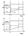
- Fig 6 shows a parasitic effect due to the fact that whenever the voltage Vout starts to change, the current mirror 30 does not operate until the voltage on the input branch 32 of the current mirror 30 reaches a certain value. For example, at start up t0, the voltage VREFIN increases rapidly. The slew rate control circuitry does not start to operate and voltage V GPM2 does not start to drop until time t1 when the voltage V OUT and hence the voltage on the input branch 32 of the current mirror 30 have reached approximately one nMOS transistor threshold voltage above the negative supply VSS. This manifests itself as a sharp rise 42, or step, of voltage V OUT followed by a controlled ramp when the voltage V OUT has reached a sufficient level for the current mirror 30 to operate and control the slew rate.
- a multiple-output current mirror 50 comprises a current reference 500 (Iref) and two current sources, 501 and 31.
- the current reference 500 from which is drawn a current Iref, is coupled to current sources 501 and 31 so that they supply currents Iref x n3 and Iref x n4 respectively, where n3 and n4 are factors determined by the transistor geometries.
- Current source 501 is connected between positive supply VDD and the input branch 32 of the current mirror 30.
- Current source 31 is coupled between supply VDD and a node coupled to both the output branch 33 of current mirror 30 and a controlling node of transistor PM2.
- Current source 501 supplies current to the input branch 32 of current mirror 30.
- the current mirror is biased, i.e. the voltage on the input branch 32 is at least one nMOS threshold voltage above the negative supply VSS. Therefore it can operate without needing the biasing via capacitor C2, and in theory, the control of the slew rate of voltage V OUT can start immediately as voltage V OUT starts to change. In fact, there is still a slight delay in the slew rate control caused by the response time of the current mirror, and a small step still occurs.
- Fig 8 represents the variation with time of voltages and currents during start-up when an embodiment is used with the elements shown in Fig 7 .
- the voltage VREFIN is increased at start-up t0. Because the control of the slew rate starts much earlier, there is a substantially smaller step 71 in the voltage V OUT . Thus, the voltage V GPM2 is reduced very soon after t0.
- Capacitor C2 is connected via a first switch SW1 to the input branch 32 of the current mirror 30 and via a second switch SW2 to supply VDD.
- the first switch SW1 Before the power-up phase, the first switch SW1 is open and the second switch SW2 is closed, thus capacitor C2 is charged up to positive supply VDD.
- switch SW2 When the start-up phase is initiated, switch SW2 is opened and switch SW1 is closed, causing capacitor C2 to be discharged into the input branch 32 of the current mirror 30, which ensures sufficient current in the input branch 32 of current mirror 30. This permits the output branch 33 of current mirror 30 to sink current, thereby turning on transistor PM2 which then turns off completely transistor PM1. This has the effect that V OUT does not start to change immediately.
- capacitor C2 is discharged to a point where the voltage on the input branch 32 of current mirror 30 is approximately an nMOS threshold voltage above the negative supply VSS.
- the feedback loop of the slew rate control starts to work, transistor PM1 is turned on and voltage V OUT starts to change with slew rate controlled in the manner described above.
- the solution represented in Fig 9 suffers less from offsets in the currents caused by matching differences between components, however it works less well for voltage scaling than the solution represented in Fig 7 .
- the solution represented in Fig 7 works better during voltage scaling but requires more attention to component matching.
- FIG. 10 shows a battery powered mobile device containing a voltage regulator incorporating one of the embodiments.
- the mobile device has a battery 80 with its negative terminal connected to negative supply VSS and its positive terminal connected to a voltage regulator 81 (LDO+VREF+SRC) incorporating an embodiment.
- a voltage regulator 81 LDO+VREF+SRC
- the second plate of capacitor C1 is connected to negative supply VSS.
- the individual members of the plurality of electronic circuits 82 have their negative supply terminals coupled to the negative supply VSS.
- the positive terminal of the battery 80 may be connected to other circuits which are not shown here.
- the voltage regulator 81 may be implemented wholly or partially in integrated circuit form or as discrete components.
Landscapes
- Engineering & Computer Science (AREA)
- Physics & Mathematics (AREA)
- Electromagnetism (AREA)
- General Physics & Mathematics (AREA)
- Radar, Positioning & Navigation (AREA)
- Automation & Control Theory (AREA)
- Continuous-Control Power Sources That Use Transistors (AREA)
Abstract
The invention concerns a circuit comprising an output stage (PM1) and a differentiator coupled between an output (2) of the output stage and a control node of the output stage. The invention also concerns a method for controlling the slew rate of an output stage.
Description
- The present invention concerns voltage regulators and amplifiers, in particular the controlling of output slew rates of such circuits.
- The power supplies of electronic equipment, either mobile or fixed, are often not stable enough for the integrated circuits they supply to operate as required. Therefore voltage regulators are frequently used to provide stable voltages having reduced levels of the transients and other variations to other circuits.
- In
Fig 1 , an example of a voltage regulator is shown. Anoperational amplifier 1 drives an output pMOS transistor PM1 which has its source connected to a high supply rail, VDD, and its drain connected to anoutput pad 2, the voltage at which is henceforth referred to as 'VOUT'. The source of transistor PM1 is connected to a negative supply VSS via a resistor bridge composed of two resistors, R1 and R2. The non-inverting input of theoperational amplifier 1 is connected to the common point between the two resistors R1, R2 so as to form a feedback loop which sets the closed loop gain of amplification circuit comprising theoperational amplifier 1 and the resistors R1, R2. The above circuit can be seen as a voltage follower, where voltage VOUT tracks the voltage at the inverting input, henceforth referred to as 'VREFIN'. Transistor PM1 is designed to provide sufficient current for the requirements of all the other circuits connected to theoutput pad 2 and so is generally a large transistor. - The
output pad 2 is connected via a capacitor C1 to the negative supply VSS. - When the regulator is powered up, the capacitor C1 is charged. Since this capacitor has to be large enough to smooth the regulated supply effectively and transistor PM1 has a high current supplying capability, the current drawn by the charging will be significant and can cause a number of problems including electromagnetic interference and transient drops in power supply voltage.
- This problem is particularly acute in battery powered mobile devices, where the resultant charging currents, which are in the order of many tens or hundreds of milliamps, can cause significant drops in the voltage delivered by the battery.
-
Fig 1 also shows, as disclosed in French patent application2872305 operational amplifier 1 receives its inverting input via a selector 3. During the power-up phase, the selector 3 connects a voltage ramp generator 4 (VRAMP) to provide voltage VREFIN. When the steady-state voltage of the voltage regulator has been reached, the selector 3 automatically connects a voltage reference 5 (VREF) to provide voltage VREFIN. The rise time of the ramp generator, which determines the slew rate of the regulator output, is chosen so as to avoid the problems described above. - However, it is often required of voltage regulators that they be able to supply multiple steady-state voltages. Such changing of the output voltage of a regulator is called voltage scaling. Whenever the voltage is increased, a large current will be drawn, as during power-up, to charge the capacitor. Thus there is also a need for controlling the slew rate during voltage scaling.
- Controlling the slew rate during start-up and voltage scaling is achieved according to an embodiment by providing a circuit comprising:
- an output stage;
- a differentiator coupled between an output of the output stage and a control node of the output stage.
- According to an embodiment, there is provided a circuit wherein the differentiator comprises:
- a limiting transistor coupled between the control node of the output stage and a first supply voltage a current mirror having an output branch coupled to a control terminal of the limiting transistor;
- a capacitor having a first terminal coupled to the output of the output stage and a second terminal coupled to an input branch of the current mirror; and
- a first current source coupled between the first supply voltage and the control terminal of the limiting transistor.
- According to an embodiment, there is provided a circuit further comprising:
- a first switch coupled between the input branch of the current mirror and the second terminal of the capacitor; and
- a second switch coupled between the first supply voltage and the second terminal of the capacitor.
- According to an embodiment, there is provided a circuit further comprising:
- a second current source coupled between the first supply voltage and the input branch of the current mirror; and
- a current reference supplying a current reference value to first and second currents sources.
- According to an embodiment, there is provided a circuit further comprising:
- an amplifier having an output coupled to a control node of the output stage;
- a voltage reference coupled to an input of the operational amplifier; and
- a feedback loop from the output of the output stage to the input of the amplifier that permits the circuit to function as a voltage regulator.
- According to an embodiment, there is provided a circuit to which a slew rate limiting circuit is coupled having an output slew rate less than 10,000 volts per second.
- According to an embodiment, there is provided a portable electronic equipment comprising a circuit according to an embodiment.
- According to an embodiment, there is provided a method of controlling the output slew rate of an output stage of a circuit, comprising the steps of:
- measuring the voltage at the output of the output stage;
- differentiating the measured voltage to produce a differentiated value;
- limiting the slew rate of a voltage applied to a controlling node of the output stage, based on the differentiated value.
- According to an embodiment, there is provided a method wherein the step of limiting the slew rate of the voltage applied to the controlling node of the output stage is achieved by supplying a current to the controlling node of the output stage in a manner proportional to the differentiated value.
- According to an embodiment, there is provided a method wherein the step of differentiating the measured voltage is achieved by differentiating the measured voltage to produce a current and multiplying the current by a predetermined value.
- Various embodiments are shown in the accompanying drawings, wherein:
-
Figure 1 schematically represents a voltage regulator incorporating a solution for controlling the output slew rate during the power-up phase of the voltage regulator. -
Figure 2 schematically represents a voltage regulator incorporating an embodiment and a solution for performing voltage scaling. -
Figure 3 represents the operation of an embodiment in terms of the variation with time of certain voltages and currents. -
Figure 4 schematically represents a voltage regulator incorporating an embodiment. -
Figure 5 schematically represents a voltage differentiator used in embodiments, simplified to illustrate the principles of operation. -
Figure 6 represents the operation of the embodiment shown inFigure 5 in terms of the variation with time of certain voltages. -
Figure 7 schematically represents the voltage differentiator ofFig 4 with circuitry for improvement of the performance during the very early stages of power-up. -
Figure 8 represents the operation of the embodiment with the improvement shown inFigure 7 in terms of the variation with time of certain voltages. -
Figure 9 schematically represents the voltage differentiator ofFig 4 with alternative circuitry for improvement of the performance during the very early stages of power-up. -
Figure 10 schematically represents an implementation of a voltage regulator incorporating an embodiment in a battery powered mobile device containing a plurality of integrated circuits. - In the description below, certain elements of a voltage regulator are implemented as described in
Fig1 and are not described further and, throughout, same references designate same elements. -
Fig 2 shows a low drop-out regulator, or LDO, including an embodiment of a slew rate control circuit 8. Adifferentiator 10 has an input receiving the output of the voltage regulator, VOUT, and drives the gate of a second pMOS transistor PM2. Transistor PM2 has its source connected to the gate of transistor PM1 and its drain connected to the positive supply VDD. Theoperational amplifier 1 receives its inverting input from a voltage reference 11 (VREF) which incorporates circuitry for providing multiple reference voltages in order to provide voltage scaling. The circuitry for providing multiple reference voltages is here represented as a selector though other solutions are possible. -
Fig 3 shows the general principles of the operation of an embodiment in terms of the variation with time of voltages and currents. Voltage VREFIN is increased at start-up t0 and at a later time t1 during voltage scaling. VOUT-A designates the voltage VOUT which would occur in a voltage regulator implemented without the embodiment. As shown by VOUT-A, the output voltage exhibitshigh slew rates 22 at start-up and during voltage scaling. Thehigh slew rates 22 of voltage VOUT-A result inlarge peaks 23 in the current IOUT-A flowing from VDD, through transistor PM1, into capacitor C1. - However, in a voltage regulator implemented with an embodiment, the
voltage differentiator 10 reduces the voltage VGPM2 at the gate of transistor PM2, in a manner substantially like that shown, in response to changes in voltage VOUT at t0 and t1. - The effect is to switch on transistor PM2 in a manner proportional to the slew rate of voltage VOUT sensed by the
voltage differentiator 10. Transistor PM2 takes control of the voltage of the gate of transistor PM1 fromoperational amplifier 1 andoperational amplifier 1 acts as a current sink for transistor PM2. - The voltage on the gate, more precisely the gate-substrate voltage, of transistor PM1 is thus limited which results in a limitation of the drain current of transistor PM1 flowing into capacitor C1. This means that the output voltage varies slower, substantially as shown by VOUT. As a consequence, the
peaks 24 of current IOUT drawn from supply VDD are reduced. -
Fig 4 shows another LDO with an embodiment where voltage scaling is performed differently than inFig 2 . The resistor bridge, R1 and R2 is replaced by a multi-tap resistor bridge R3 having a number of intermediate taps and the reference voltage tooperational amplifier 1 is provided by a fixed voltage reference 5 (VREF). One of the intermediate taps of the multi-tap resistor bridge R3 is connected to the non-inverting input of theoperational amplifier 1 so as to set the gain of theoperational amplifier 1. By connecting the non-inverting input of theoperational amplifier 1 to a different intermediate tap of the multi-tap resistor bridge R3, the gain of theoperational amplifier 1 can be varied so as to obtain a variation of voltage VOUT, i.e. voltage scaling, without changing the voltage VREFIN. -
Fig 5 shows an exemplary differentiator, usable in an embodiment. Between theoutput pad 2 and aninput branch 32 of a current mirror 30 (current mirror 1:n), is connected a capacitor C2. To the gate of transistor PM2 is connected anoutput branch 33 of thecurrent mirror 30. Acurrent source 31, supplying a current Iref, is connected between the gate of transistor PM2 and supply VDD. - The change of voltage VOUT is converted into a current I1 by capacitor C2 and fed into the
input branch 32 of thecurrent mirror 30 which, in turn, multiplies it by a predetermined ratio to create a current I2. When current I2 is greater than current Iref, the voltage at the gate of transistor PM2 is reduced and transistor PM2 is turned on accordingly. - Referring back to
Fig 3 , whenever the voltage VOUT starts to change, the current I2 increases rapidly and voltage VGPM2 drops rapidly. This negative feedback loop then stabilizes to a stable state condition where I2 is equal to Iref and voltage VGPM2 and the slew rate of voltage VOUT are constant. Eventually voltage VOUT becomes close to its target value and transistor PM1 starts to be shut down. This reduces the slew rate which shuts down the slew rate control circuitry. Finallyoperational amplifier 1 takes control again and the voltage VOUT becomes constant, the slew rate control circuitry is shut off completely and voltage VGPM2 is close to the voltage at VDD. - The operation of this embodiment is described by the equations below;
- In the stable state condition, the current I1 is given by

- Via the
current mirror 30 we have
- Where Iref is the current supplied by the
current source 31 and n is the ratio of thecurrent mirror 30. - Thus we have

where SLR is the slew rate of VOUT. -
Fig 6 shows a parasitic effect due to the fact that whenever the voltage Vout starts to change, thecurrent mirror 30 does not operate until the voltage on theinput branch 32 of thecurrent mirror 30 reaches a certain value. For example, at start up t0, the voltage VREFIN increases rapidly. The slew rate control circuitry does not start to operate and voltage VGPM2 does not start to drop until time t1 when the voltage VOUT and hence the voltage on theinput branch 32 of thecurrent mirror 30 have reached approximately one nMOS transistor threshold voltage above the negative supply VSS. This manifests itself as asharp rise 42, or step, of voltage VOUT followed by a controlled ramp when the voltage VOUT has reached a sufficient level for thecurrent mirror 30 to operate and control the slew rate. -
Fig 7 shows a solution to overcome the above parasitic effect. A multiple-outputcurrent mirror 50 comprises a current reference 500 (Iref) and two current sources, 501 and 31. Thecurrent reference 500, from which is drawn a current Iref, is coupled tocurrent sources Current source 501 is connected between positive supply VDD and theinput branch 32 of thecurrent mirror 30.Current source 31 is coupled between supply VDD and a node coupled to both theoutput branch 33 ofcurrent mirror 30 and a controlling node of transistor PM2. -
Current source 501 supplies current to theinput branch 32 ofcurrent mirror 30. This means that the current mirror is biased, i.e. the voltage on theinput branch 32 is at least one nMOS threshold voltage above the negative supply VSS. Therefore it can operate without needing the biasing via capacitor C2, and in theory, the control of the slew rate of voltage VOUT can start immediately as voltage VOUT starts to change. In fact, there is still a slight delay in the slew rate control caused by the response time of the current mirror, and a small step still occurs. -
Fig 8 represents the variation with time of voltages and currents during start-up when an embodiment is used with the elements shown inFig 7 . - The voltage VREFIN is increased at start-up t0. Because the control of the slew rate starts much earlier, there is a substantially
smaller step 71 in the voltage VOUT. Thus, the voltage VGPM2 is reduced very soon after t0. - For the solution shown in
Fig 7 , the slew rate SLR of voltage VOUT is given by;
- One of ordinary skill will be able to choose numbers n3 and n4 along with the other components of the circuits so that the
current mirror 30 is correctly biased at start-up and can provide the desired slew rate limiting. -
Fig 9 shows another solution to the above parasitic effect. Capacitor C2 is connected via a first switch SW1 to theinput branch 32 of thecurrent mirror 30 and via a second switch SW2 to supply VDD. - Before the power-up phase, the first switch SW1 is open and the second switch SW2 is closed, thus capacitor C2 is charged up to positive supply VDD. When the start-up phase is initiated, switch SW2 is opened and switch SW1 is closed, causing capacitor C2 to be discharged into the
input branch 32 of thecurrent mirror 30, which ensures sufficient current in theinput branch 32 ofcurrent mirror 30. This permits theoutput branch 33 ofcurrent mirror 30 to sink current, thereby turning on transistor PM2 which then turns off completely transistor PM1. This has the effect that VOUT does not start to change immediately. - After a certain time, capacitor C2 is discharged to a point where the voltage on the
input branch 32 ofcurrent mirror 30 is approximately an nMOS threshold voltage above the negative supply VSS. At this point, the feedback loop of the slew rate control starts to work, transistor PM1 is turned on and voltage VOUT starts to change with slew rate controlled in the manner described above. - Once the steady state value of voltage VOUT has been reached the
current mirror 30 switches off and thecurrent source 31 turns off automatically. - The solution represented in
Fig 9 suffers less from offsets in the currents caused by matching differences between components, however it works less well for voltage scaling than the solution represented inFig 7 . The solution represented inFig 7 works better during voltage scaling but requires more attention to component matching. - The above description shows only embodiments that control the slew rate of increases of voltage VOUT. However, one ordinarily versed in the art will appreciate that an implementation which limits the slew rate when voltage VOUT is decreasing can be obtained by connecting an nMOS transistor device between the output of the
operational amplifier 1 and negative supply VSS or indeed connecting MOS transistor devices to both positive supply VDD and negative supply VSS to obtain control of the slew rate in both directions. -
Figure 10 shows a battery powered mobile device containing a voltage regulator incorporating one of the embodiments. Amongst other circuits, the mobile device has abattery 80 with its negative terminal connected to negative supply VSS and its positive terminal connected to a voltage regulator 81 (LDO+VREF+SRC) incorporating an embodiment. To the output of thevoltage regulator 81, are connected, firstly the first plate of a filter capacitor C1 and, secondly, the positive supply terminals of a plurality of electronic circuits 82 (IC1-ICn). The second plate of capacitor C1 is connected to negative supply VSS. - The individual members of the plurality of
electronic circuits 82 have their negative supply terminals coupled to the negative supply VSS. The positive terminal of thebattery 80 may be connected to other circuits which are not shown here. Thevoltage regulator 81 may be implemented wholly or partially in integrated circuit form or as discrete components. - The detailed description set forth above, with the appended drawings, is intended to provide a description of the preferred embodiments and features, and is not intended to represent the only form nor imply the only combination of the features. It is to be understood that the same function may be accomplished by different embodiments which are intended to be encompassed by the scope of the present invention. For instance, voltage regulators are discussed here in detail but this invention could be implemented with other circuits, for example, but not limited to, an amplifier, which has an output having to drive a load, in order to control the slew rates of that output whenever the voltage at that output is changed.
Claims (10)
- A circuit comprising:- an output stage (PM1);- a differentiator coupled between an output (2) of the output stage (PM1) and a control node of the output stage.
- A circuit according to claim 1 wherein said differentiator comprises:- a limiting transistor (PM2) coupled between the control node of said output stage (PM1) and a first supply voltage (VDD)a current mirror (30) having an output branch (33) coupled to a control terminal of said limiting transistor;- a capacitor (C2) having a first terminal coupled to the output (2) of the output stage (PM1) and a second terminal coupled to an input branch (32) of said current mirror (30); and- a first current source (31) coupled between the first supply voltage (VDD) and said control terminal of the limiting transistor (PM2).
- A circuit according to claim 2 further comprising:- a first switch (SW1) coupled between the input branch (32) of the current mirror (30) and the second terminal of the capacitor (C2); and- a second switch (SW2) coupled between the first supply voltage (VDD) and the second terminal of the capacitor (C2).
- A circuit according to claim 2 further comprising:- a second current source (501) coupled between the first supply voltage (VDD) and the input branch (32) of the current mirror (30); and- a current reference (500) supplying a current reference value to first and second currents sources.
- A circuit according to one of claims 1 to 4 further comprising:- an amplifier (1) having an output coupled to a control node of said output stage (PM1);- a voltage reference (VREF) coupled to an input of said operational amplifier (1); and- a feedback loop from the output (2) of the output stage (PM1) to said input of the amplifier (1) that permits the circuit to function as a voltage regulator.
- A circuit to which a slew rate limiting circuit (10, PM2) according to one of claims 1 to 6 is coupled having an output slew rate less than 10,000 volts per second.
- A portable electronic equipment comprising a circuit according to one of claims 1 to 6.
- A method of controlling the output slew rate of an output stage of a circuit, comprising the steps of:- measuring the voltage at the output (2) of the output stage (PM1);- differentiating the measured voltage to produce a differentiated value;- limiting the slew rate of a voltage applied to a controlling node of said output stage (PM1), based on said differentiated value.
- A method according to claim 8 wherein the step of limiting the slew rate of the voltage applied to said controlling node of the output stage (PM1) is achieved by supplying a current to said controlling node of the output stage in a manner proportional to the differentiated value.
- A method according to claim 9 wherein the step of differentiating the measured voltage is achieved by differentiating the measured voltage to produce a current and multiplying the current by a predetermined value.
Priority Applications (1)
| Application Number | Priority Date | Filing Date | Title |
|---|---|---|---|
| EP08305162A EP2120123A1 (en) | 2008-05-12 | 2008-05-12 | Slew rate control |
Applications Claiming Priority (1)
| Application Number | Priority Date | Filing Date | Title |
|---|---|---|---|
| EP08305162A EP2120123A1 (en) | 2008-05-12 | 2008-05-12 | Slew rate control |
Publications (1)
| Publication Number | Publication Date |
|---|---|
| EP2120123A1 true EP2120123A1 (en) | 2009-11-18 |
Family
ID=39758447
Family Applications (1)
| Application Number | Title | Priority Date | Filing Date |
|---|---|---|---|
| EP08305162A Withdrawn EP2120123A1 (en) | 2008-05-12 | 2008-05-12 | Slew rate control |
Country Status (1)
| Country | Link |
|---|---|
| EP (1) | EP2120123A1 (en) |
Cited By (14)
| Publication number | Priority date | Publication date | Assignee | Title |
|---|---|---|---|---|
| CN102789256A (en) * | 2012-08-29 | 2012-11-21 | 上海宏力半导体制造有限公司 | Low-pressure-difference linear stabilizer |
| CN103163928A (en) * | 2011-12-19 | 2013-06-19 | 凹凸电子(武汉)有限公司 | Circuit and method for providing a reference signal |
| US20130222028A1 (en) * | 2012-02-24 | 2013-08-29 | Qualcomm Incorporated | Method and apparatus for load switch controller |
| CN103399607A (en) * | 2013-07-29 | 2013-11-20 | 电子科技大学 | High-PSR (high power supply rejection) low-dropout regulator with slew rate enhancement circuit integrated thereto |
| CN103412602A (en) * | 2013-08-27 | 2013-11-27 | 吴小刚 | Non-capacitive low-dropout linear voltage regulator |
| CN103592989A (en) * | 2012-08-16 | 2014-02-19 | 成都锐成芯微科技有限责任公司 | Low quiescent dissipation rapid transient response non-output capacitance LDO (low drop out regulator) circuit |
| CN103729003A (en) * | 2012-10-15 | 2014-04-16 | 上海聚纳科电子有限公司 | Low drop-out linear regulated power supply without off-chip capacitor |
| CN104950976A (en) * | 2015-05-20 | 2015-09-30 | 泰斗微电子科技有限公司 | Voltage stabilizing circuit based on slew rate increasing |
| US9294078B1 (en) | 2014-09-09 | 2016-03-22 | Reescale Semiconductor,Inc. | Voltage-driver circuit with dynamic slew rate control |
| US9331568B2 (en) | 2012-03-15 | 2016-05-03 | Qualcomm Incorporated | Method and apparatus for load switch controller with tracking to support DDR termination |
| US9385587B2 (en) | 2013-03-14 | 2016-07-05 | Sandisk Technologies Llc | Controlled start-up of a linear voltage regulator where input supply voltage is higher than device operational voltage |
| CN107315441A (en) * | 2017-07-03 | 2017-11-03 | 电子科技大学 | Low pressure difference linear voltage regulator on a kind of piece with fast transient response |
| CN108919872A (en) * | 2018-06-25 | 2018-11-30 | 北京集创北方科技股份有限公司 | Low pressure difference linear voltage regulator and its method for stabilizing voltage |
| CN114089802A (en) * | 2021-11-30 | 2022-02-25 | 荣耀终端有限公司 | Power supply circuit, terminal device and voltage control method |
Citations (5)
| Publication number | Priority date | Publication date | Assignee | Title |
|---|---|---|---|---|
| EP0508171A1 (en) * | 1991-04-11 | 1992-10-14 | Siemens Aktiengesellschaft | Switching mode power output stage for inductive loads |
| JPH07135452A (en) * | 1993-11-11 | 1995-05-23 | Nec Corp | Current comparator |
| EP0926826A1 (en) * | 1997-12-18 | 1999-06-30 | ABB Research Ltd. | Method and device in power transistor |
| US6040686A (en) * | 1999-01-07 | 2000-03-21 | Linear Technology Corporation | Low noise step-down switching regulator circuits with programmable slew rate limiter and methods of use |
| FR2872305A1 (en) | 2004-06-24 | 2005-12-30 | St Microelectronics Sa | METHOD FOR CONTROLLING THE OPERATION OF A LOW VOLTAGE DROP REGULATOR AND CORRESPONDING INTEGRATED CIRCUIT |
-
2008
- 2008-05-12 EP EP08305162A patent/EP2120123A1/en not_active Withdrawn
Patent Citations (5)
| Publication number | Priority date | Publication date | Assignee | Title |
|---|---|---|---|---|
| EP0508171A1 (en) * | 1991-04-11 | 1992-10-14 | Siemens Aktiengesellschaft | Switching mode power output stage for inductive loads |
| JPH07135452A (en) * | 1993-11-11 | 1995-05-23 | Nec Corp | Current comparator |
| EP0926826A1 (en) * | 1997-12-18 | 1999-06-30 | ABB Research Ltd. | Method and device in power transistor |
| US6040686A (en) * | 1999-01-07 | 2000-03-21 | Linear Technology Corporation | Low noise step-down switching regulator circuits with programmable slew rate limiter and methods of use |
| FR2872305A1 (en) | 2004-06-24 | 2005-12-30 | St Microelectronics Sa | METHOD FOR CONTROLLING THE OPERATION OF A LOW VOLTAGE DROP REGULATOR AND CORRESPONDING INTEGRATED CIRCUIT |
Non-Patent Citations (1)
| Title |
|---|
| J WEBSTER: "Wiley Encyclopedia of Electrical and Electronics Engineering", 1999, JOHN WILEY & SONS, INC, XP002496975 * |
Cited By (24)
| Publication number | Priority date | Publication date | Assignee | Title |
|---|---|---|---|---|
| CN103163928A (en) * | 2011-12-19 | 2013-06-19 | 凹凸电子(武汉)有限公司 | Circuit and method for providing a reference signal |
| CN103163928B (en) * | 2011-12-19 | 2015-03-11 | 凹凸电子(武汉)有限公司 | Circuit and method for providing a reference signal |
| US20130222028A1 (en) * | 2012-02-24 | 2013-08-29 | Qualcomm Incorporated | Method and apparatus for load switch controller |
| US9312835B2 (en) * | 2012-02-24 | 2016-04-12 | Qualcomm, Inc | Load switch controller with slew rate control |
| US9331568B2 (en) | 2012-03-15 | 2016-05-03 | Qualcomm Incorporated | Method and apparatus for load switch controller with tracking to support DDR termination |
| CN103592989B (en) * | 2012-08-16 | 2016-08-24 | 成都锐成芯微科技有限责任公司 | The OCL output capacitance-less LDO circuit of low speed paper tape reader static power disspation fast transient response |
| CN103592989A (en) * | 2012-08-16 | 2014-02-19 | 成都锐成芯微科技有限责任公司 | Low quiescent dissipation rapid transient response non-output capacitance LDO (low drop out regulator) circuit |
| CN102789256B (en) * | 2012-08-29 | 2016-03-23 | 上海华虹宏力半导体制造有限公司 | Low pressure difference linear voltage regulator |
| CN102789256A (en) * | 2012-08-29 | 2012-11-21 | 上海宏力半导体制造有限公司 | Low-pressure-difference linear stabilizer |
| CN103729003A (en) * | 2012-10-15 | 2014-04-16 | 上海聚纳科电子有限公司 | Low drop-out linear regulated power supply without off-chip capacitor |
| CN103729003B (en) * | 2012-10-15 | 2016-03-09 | 上海聚纳科电子有限公司 | Without the low pressure difference linearity source of stable pressure of the outer electric capacity of sheet |
| US9385587B2 (en) | 2013-03-14 | 2016-07-05 | Sandisk Technologies Llc | Controlled start-up of a linear voltage regulator where input supply voltage is higher than device operational voltage |
| CN103399607A (en) * | 2013-07-29 | 2013-11-20 | 电子科技大学 | High-PSR (high power supply rejection) low-dropout regulator with slew rate enhancement circuit integrated thereto |
| CN103399607B (en) * | 2013-07-29 | 2015-09-02 | 电子科技大学 | The high PSR low pressure difference linear voltage regulator of integrated slew rate enhancing circuit |
| CN103412602A (en) * | 2013-08-27 | 2013-11-27 | 吴小刚 | Non-capacitive low-dropout linear voltage regulator |
| US9294078B1 (en) | 2014-09-09 | 2016-03-22 | Reescale Semiconductor,Inc. | Voltage-driver circuit with dynamic slew rate control |
| CN104950976A (en) * | 2015-05-20 | 2015-09-30 | 泰斗微电子科技有限公司 | Voltage stabilizing circuit based on slew rate increasing |
| CN107315441A (en) * | 2017-07-03 | 2017-11-03 | 电子科技大学 | Low pressure difference linear voltage regulator on a kind of piece with fast transient response |
| CN108919872A (en) * | 2018-06-25 | 2018-11-30 | 北京集创北方科技股份有限公司 | Low pressure difference linear voltage regulator and its method for stabilizing voltage |
| WO2020001271A1 (en) * | 2018-06-25 | 2020-01-02 | 北京集创北方科技股份有限公司 | Low dropout regulator and voltage stabilization method therefor |
| KR20200014388A (en) * | 2018-06-25 | 2020-02-10 | 칩원 테크놀로지(베이징) 컴퍼니 리미티드 | Low Voltage Drop Regulator and Its Voltage Stabilization Method |
| CN108919872B (en) * | 2018-06-25 | 2020-06-09 | 北京集创北方科技股份有限公司 | Low dropout linear regulator and voltage stabilizing method thereof |
| US11061422B2 (en) | 2018-06-25 | 2021-07-13 | Chipone Technology (Beijing) Co., Ltd. | Low dropout linear regulator and voltage stabilizing method therefor |
| CN114089802A (en) * | 2021-11-30 | 2022-02-25 | 荣耀终端有限公司 | Power supply circuit, terminal device and voltage control method |
Similar Documents
| Publication | Publication Date | Title |
|---|---|---|
| US7199565B1 (en) | Low-dropout voltage regulator with a voltage slew rate efficient transient response boost circuit | |
| EP2527946B1 (en) | Current limitation for low dropout (LDO) voltage regulator | |
| US9223329B2 (en) | Low drop out voltage regulator with operational transconductance amplifier and related method of generating a regulated voltage | |
| US6208127B1 (en) | Methods and apparatus to predictably change the output voltage of regulators | |
| US10459470B2 (en) | Voltage regulator and method for providing an output voltage with reduced voltage ripple | |
| EP2846213B1 (en) | Method and apparatus for limiting startup inrush current for low dropout regulator | |
| EP1378808B1 (en) | LDO regulator with wide output load range and fast internal loop | |
| US6388433B2 (en) | Linear regulator with low overshooting in transient state | |
| US8598861B2 (en) | Circuit and method for providing a reference signal | |
| US8334681B2 (en) | Domino voltage regulator (DVR) | |
| US8217638B1 (en) | Linear regulation for use with electronic circuits | |
| US7615977B2 (en) | Linear voltage regulator and method of limiting the current in such a regulator | |
| EP2551743B1 (en) | Low-dropout regulator and method for voltage regulation | |
| JP5008472B2 (en) | Voltage regulator | |
| US7969127B1 (en) | Start-up circuit for a shunt regulator | |
| US11435768B2 (en) | N-channel input pair voltage regulator with soft start and current limitation circuitry | |
| EP0846996A1 (en) | Power transistor control circuit for a voltage regulator | |
| TW200525868A (en) | Power supply apparatus capable of supplying a stable converted voltage | |
| US8129962B2 (en) | Low dropout voltage regulator with clamping | |
| CN116360535A (en) | Integrated User Programmable Slew Rate Controlled Soft Starter for LDOs | |
| US20070210726A1 (en) | Current limiting circuit | |
| CN114995564B (en) | Starting circuit, starting method and electronic equipment | |
| CN108459644B (en) | Low dropout voltage stabilizer and method of operation | |
| US11709515B1 (en) | Voltage regulator with n-type power switch | |
| CN116185113A (en) | Soft start circuit, low dropout linear regulator, chip and electronic equipment |
Legal Events
| Date | Code | Title | Description |
|---|---|---|---|
| PUAI | Public reference made under article 153(3) epc to a published international application that has entered the european phase |
Free format text: ORIGINAL CODE: 0009012 |
|
| AK | Designated contracting states |
Kind code of ref document: A1 Designated state(s): AT BE BG CH CY CZ DE DK EE ES FI FR GB GR HR HU IE IS IT LI LT LU LV MC MT NL NO PL PT RO SE SI SK TR |
|
| AX | Request for extension of the european patent |
Extension state: AL BA MK RS |
|
| AKX | Designation fees paid | ||
| REG | Reference to a national code |
Ref country code: DE Ref legal event code: 8566 |
|
| STAA | Information on the status of an ep patent application or granted ep patent |
Free format text: STATUS: THE APPLICATION IS DEEMED TO BE WITHDRAWN |
|
| 18D | Application deemed to be withdrawn |
Effective date: 20100519 |