EP2118900B1 - Sram with elastic power supply for improved read and write margins - Google Patents
Sram with elastic power supply for improved read and write margins Download PDFInfo
- Publication number
- EP2118900B1 EP2118900B1 EP08728583A EP08728583A EP2118900B1 EP 2118900 B1 EP2118900 B1 EP 2118900B1 EP 08728583 A EP08728583 A EP 08728583A EP 08728583 A EP08728583 A EP 08728583A EP 2118900 B1 EP2118900 B1 EP 2118900B1
- Authority
- EP
- European Patent Office
- Prior art keywords
- power supply
- supply line
- memory device
- reference voltage
- sram
- Prior art date
- Legal status (The legal status is an assumption and is not a legal conclusion. Google has not performed a legal analysis and makes no representation as to the accuracy of the status listed.)
- Active
Links
Images

Classifications
-
- G—PHYSICS
- G11—INFORMATION STORAGE
- G11C—STATIC STORES
- G11C11/00—Digital stores characterised by the use of particular electric or magnetic storage elements; Storage elements therefor
- G11C11/21—Digital stores characterised by the use of particular electric or magnetic storage elements; Storage elements therefor using electric elements
- G11C11/34—Digital stores characterised by the use of particular electric or magnetic storage elements; Storage elements therefor using electric elements using semiconductor devices
- G11C11/40—Digital stores characterised by the use of particular electric or magnetic storage elements; Storage elements therefor using electric elements using semiconductor devices using transistors
- G11C11/41—Digital stores characterised by the use of particular electric or magnetic storage elements; Storage elements therefor using electric elements using semiconductor devices using transistors forming static cells with positive feedback, i.e. cells not needing refreshing or charge regeneration, e.g. bistable multivibrator or Schmitt trigger
- G11C11/413—Auxiliary circuits, e.g. for addressing, decoding, driving, writing, sensing, timing or power reduction
- G11C11/417—Auxiliary circuits, e.g. for addressing, decoding, driving, writing, sensing, timing or power reduction for memory cells of the field-effect type
- G11C11/419—Read-write [R-W] circuits
-
- G—PHYSICS
- G11—INFORMATION STORAGE
- G11C—STATIC STORES
- G11C11/00—Digital stores characterised by the use of particular electric or magnetic storage elements; Storage elements therefor
- G11C11/21—Digital stores characterised by the use of particular electric or magnetic storage elements; Storage elements therefor using electric elements
- G11C11/34—Digital stores characterised by the use of particular electric or magnetic storage elements; Storage elements therefor using electric elements using semiconductor devices
- G11C11/40—Digital stores characterised by the use of particular electric or magnetic storage elements; Storage elements therefor using electric elements using semiconductor devices using transistors
- G11C11/41—Digital stores characterised by the use of particular electric or magnetic storage elements; Storage elements therefor using electric elements using semiconductor devices using transistors forming static cells with positive feedback, i.e. cells not needing refreshing or charge regeneration, e.g. bistable multivibrator or Schmitt trigger
- G11C11/413—Auxiliary circuits, e.g. for addressing, decoding, driving, writing, sensing, timing or power reduction
- G11C11/417—Auxiliary circuits, e.g. for addressing, decoding, driving, writing, sensing, timing or power reduction for memory cells of the field-effect type
-
- G—PHYSICS
- G11—INFORMATION STORAGE
- G11C—STATIC STORES
- G11C5/00—Details of stores covered by group G11C11/00
- G11C5/14—Power supply arrangements, e.g. power down, chip selection or deselection, layout of wirings or power grids, or multiple supply levels
- G11C5/147—Voltage reference generators, voltage or current regulators; Internally lowered supply levels; Compensation for voltage drops
Definitions
- Static random access memory (SRAM) cells can be implemented using cross- coupled logic gates which maintain logic states representing data values. Ideally, SRAM cells should hold their stored logic states despite possible changes in voltage, temperature, or other operating conditions. Unfortunately, existing SRAM cell designs often fail to provide high degrees of read stability.
- the internal nodes of the SRAM cell may be vulnerable to read disturbance.
- the internal SRAM nodes may be inadvertently charged through the access transistors to rise above a trip voltage of the SRAM cell, thereby causing the SRAM cell to inadvertently switch logic states.
- the Static Noise Margin is a "figure of merit" which measures read stability and read margin. See Benton H. Calhoun and Anantha Chandrakasan, Analyzing Static Noise Margin for Subthreshold SRAM in 65nm CMOS, http://www-mtl.mit.edu/researchgroups/icsystems/pubs/conferences/2005/bcalhoun_esscirc2005_pap er.pdf (September 2005 ). See also Evert Seevinck, Frans J. List, Jan Lohstroh, Static- Noise Margin Analysis of MOS SRAM Cells, IEEE JOURNAL OF SOLID-STATE CIRCUITS, Vol. SC-22, No. 5, pp. 748-754 (October 1987 ).
- a designer can reduce the ratio between the sizes of the NMOS driver transistor and the NMOS pass transistor in a SRAM cell.
- the variation from the desired ratio between the driver and the pass transistor can be significant.
- the variation from the desired ratio can be as large as 10:1.
- an additional pair of PMOS transistors is added to the SRAM cell so that the overall ratio of the PMOS transistors to the NMOS transistors in the SRAM cell is minimized.
- the additional pair of PMOS transistors also makes the SNM curve symmetrical, resulting in a wider "eye.” This approach tries to minimize the variation in size ratio between the NMOS driver and pass transistors by counter-balancing voltages in the SRAM cell.
- adding a pair of PMOS transistors alleviates the problem slightly, such an approach has its own drawbacks. The PMOS transistors eventually get so strong that they pull nodes in the SRAM cell high when they should not be pulled high, leading to poor read stability.
- US 7,092,280 discloses a CMOS static random access memory (SRAM) array with dynamically asymmetric cells, an integrated circuit (IC) chip including the SRAM and a method of accessing data in the SRAM.
- SRAM static random access memory
- IC integrated circuit
- Each column of cells is connected to a pair of column supply lines supplying power to the column.
- a higher voltage is applied to one column supply line in each pair of the columns being accessed to unbalance cells in the columns being accessed. Unbalanced cells become asymmetric during accesses and the supply imbalance favors the data state being written/read.
- An embodiment of the invention enables an increase read stability, decrease read disturbance, improve the SNM, and improve read margin for an SRAM memory cell.
- An embodiment of this invention provides a memory device that includes: a reference voltage; a first and a second power supply line; a static random access memory (SRAM) cell with cross-coupled first and second logic gates, with the first power supply line and the second power supply line respectively supplying the first and the second logic gates; and an elastic power header device provides, during a write operation of the first SRAM cell, different power levels on the first power supply line and the second power supply line and that provides, during a read operation, a programmable resistance in the first power supply line and the second power supply line.
- SRAM static random access memory
- an elastic power header device that provides a memory device with a first and second power supply lines.
- the elastic power device includes: (1) a first path having first and second power differences between a reference voltage and, respectively, the first and second power supply lines; (2) second and third paths that are coupled between the reference voltage and, respectively, the first and second power supply lines wherein, during a write operation, resistance in either the second path or the third path is varied to provide a power difference between the first and second power supply lines; and (3) fourth and fifth paths that are coupled between the reference voltage and, respectively, the first and second power supply lines wherein, during a read operation, a programmable resistance is provided in a selected one of the fourth path or the fifth path.
- Various embodiments of this invention include methods of operating the above or similar memory devices, and computer-readable media that use hardware description languages (HDLs) to describe the above or similar memory devices.
- HDLs hardware description languages
- FIG. 1 is a conceptual block diagram showing circuit 100, in which a number of SRAM cells are connected to an elastic power header device, in accordance with one embodiment of the invention.
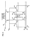
- FIG. 2 shows circuit 200, which implements an SRAM cell suitable for use as any of SRAM cells 110 of Figure 1 , in accordance with an embodiment of the invention.
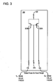
- FIG. 3 illustrates circuit 300, which implements an elastic power header device in accordance with an embodiment of the invention.
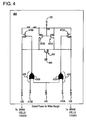
- FIG. 4 illustrates circuit 400, which may be also be used to implement elastic power header device 180 of Figure 1 , in accordance with another embodiment of the invention.
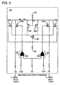
- FIG. 5 illustrates circuit 500, which implements elastic power header device 180 of Figure 1 , in accordance with another embodiment of the invention.
- Figure 6 shows circuit 600, which provides a low-going pulse, which may be used to provide write enable signal 425 during a read or write operation in elastic power header circuit 180 of Figure 1 , in accordance with an embodiment of the invention.
- Figure 7 illustrates an example of a content-addressable memory (CAM) cell that may be implemented using the SRAM cell circuits disclosed above.
- CAM content-addressable memory
- an elastic power header device improves the read margin and read stability of a memory cell, such as an SRAM cell.
- an elastic power header device described herein acts as a programmable resistance to allow the power supply lines to reach a voltage equal to a desired reference voltage, without experiencing a threshold drop. Therefore, an elastic power header device of the present invention provides additional flexibility in both read margin and read stability. The additional flexibility may also be varied with an adjustment voltage, which can be used to fine-tune and control the read margin.
- Figure 1 is a conceptual block diagram showing circuit 100, in which a number of SRAM cells 110 are connected to elastic power header device 180, in accordance with an embodiment of the invention.
- elastic power header device 180 Several possible circuit implementations for elastic power header device 180 are illustrated in Figs. 3 through 5 , as further described herein.
- SRAM cells 110 are each connected to power supply lines 125 and 135.
- each of SRAM cells 110 may be implemented by cross-coupled logic gates (e.g., cross-coupled inverters).
- Elastic power header device 180 may also act as "split power switch” that provide voltages of power supply lines 125 and 135 from power supply voltage 120 ("V dd ")
- Split power switches are discussed, for example, in U.S. patent application, entitled “Split Power Switch for Memory Cells" ("Copending Application"), serial no. 60/888,006, filed on February 2, 2007 .
- voltages of power supply lines 125 and 135 are slightly different, to facilitate writing into an SRAM cell.
- the disclosure of the Copending Application is hereby incorporated by reference to provide background for the split power technique.
- Elastic power header device 180 selectively adjusts the voltages provided to power supply lines 125 and 135, in response to one or more control signals 150.
- elastic power header device 180 may be configured to provide substantially reference voltage 120 during a read operation, while allowing the voltage of one of power supply lines 125 and 135 to fall during an appropriate write operation of SRAM cells 110.
- SRAM cells 110 are shown in Figure 1 as a single column of memory cells connected to a single split power switch 140, it is understood that Figure 1 is merely illustrative.
- additional groups of SRAM cells 110 connect to power supply lines 125 and 135, and additional elastic power header devices 180 may be used to provide power to these additional groups of SRAM cells.
- the additional SRAM cells may share power supply lines 125 and 135 under control by a single elastic power header device 180.
- the single column of memory cells may be split into multiple sub-columns, each sub-column having its own power supply lines 125 and 135 but sharing the same bit line.
- bit lines 270 and 280 are connected with each of SRAM cells 110-1 through 110-N.
- SRAM cells 110-1 through 110-N may share bitlines 270 and 280.
- bit lines may not be shared by all of SRAM cells 110-1 through 110-N.
- a first set of bit lines may be provided to SRAM cells 110-1 and 110-2, and a second set of bit lines may be provided to SRAM cell 110-N.
- SRAM cells 110-1 and 110-2 may use bit lines separate from those used by SRAM cell 110-N.
- any desired combination of shared and/or unshared bit lines may be used.
- FIG. 2 shows circuit 200, which implements an SRAM cell that is suitable for use as any of SRAM cells 110 of Figure 1 , in accordance with an embodiment of the invention.
- circuit 200 includes cross-coupled inverters 225 and 245 implemented by PMOS transistors 210 and 230 and NMOS transistors 220 and 240, respectively.
- PMOS transistor 210 connects to power supply line 135, while PMOS transistor 230 connects to power supply line 125.
- NMOS transistors 220 and 240 each connect to reference voltage 295 ("V ss ") which may correspond, for example, to ground.
- Figure 2 further shows that n-well and p-well voltages 205 and 215 (labeled V nw and V pw , respectively), each may differ from either reference voltage 120 or reference voltage 295.
- the n-well voltage 205 must be greater than or equal to the maximum of power supply lines 125 or 135.
- the n-well voltage is often the same line as reference voltage 120 ("V dd ").
- the n-well voltage 205 is not the same line as either power supply lines 125 or 135, but it may happen to have the same voltage as power supply lines 125 or 135.
- Access or pass transistors 250 and 260 connect to word line 290 and bit lines 270 and 280, and internal nodes 255 and 265, respectively.
- elastic power header device 180 provides that the voltage of each of power supply lines 125 and 135 is approximately reference voltage 120.
- elastic power header device 180 maintains each of power supply lines 125 and 135 at approximately reference voltage 120.
- bit lines 270 and 280 are precharged to an intermediate voltage, and word line 290 may then be set to a logic high voltage, so that access transistors 250 and 260 becomes conducting to allow inverters 225 and 245 to drive the stored logic values at nodes 255 and 265 to bit lines 270 and 280.
- elastic power header device 180 permits the voltage of power supply line 125 to fall below reference voltage 120, while maintaining the voltage of power supply line 135 at approximately reference voltage 120.
- nodes 255 and 265 are initially at logic low and logic high, respectively.
- NMOS transistor 220 and PMOS transistor 230 are conducting, while PMOS transistors 210 and NMOS transistor 240 are non-conducting.
- bit lines 270 and 280 are driven to logic high and logic low, respectively, by appropriate write circuitry (not shown), as word line 290 is driven to logic high to turn on access transistors 250 and 260. Accordingly, bit line 280 pulls node 265 down from logic high to logic low. Because PMOS transistor 230 is initially conducting, its current acts to pull up the voltage at node 265. However, with power supply line 125 falling below reference voltage 120, resulting in less current flowing in transistor 230 than would otherwise flow, bit line 280 can more rapidly turn on PMOS transistor 210 which, in turn, turns on NMOS transistor 240 to pull down node 265. By maintaining the voltage of power supply line 135 approximately at reference voltage 120, transistor 210 allows the voltage at node 255 to be more rapidly pulled up.
- writing the opposite logic state i.e., to bring node 255 to logic low and node 265 to logic high
- writing the opposite logic state may be facilitated by allowing power supply line 135 to fall below reference voltage 120, while maintaining power supply line 125 at approximately reference voltage 120.
- FIG 3 illustrates circuit 300, which implements an elastic power header device (e.g., elastic power header device 180 of Figure 1 ), in accordance with an embodiment of the invention.
- Circuit 300 improves read margin.
- Circuit 300 includes resistive transistors 320A and 320B, which connect reference voltage 120 to power supply lines 125 (labeled “levdd”) and 135 (labeled “rivdd”), respectively.
- Transistors 320A and 320B are shown in Figure 3 as being implemented by PMOS transistors.
- Adjustment voltage 345 (labeled "vref"), provided at the gate electrodes of resistive transistors 320A and 302B, adjusts the effective resistance of transistors 320A and 320B.
- adjustment voltage 345 (1) may be fixed at a predetermined voltage, (2) may be a dynamically adjusted voltage, or (3) may be controlled by a thermal-sensing self-calibration circuit to automatically adjust to a proper voltage.
- resistive transistors 320A and 320B When maintained in the linear region, resistive transistors 320A and 320B can each pull power supply lines 125 and 135 to reference voltage 120. Within this region, the adjustment voltage 345 flexibly fine-tunes main resistive transistors 320A and 320B to be as close to reference voltage 120 as desired, taking into consideration the current drawn by the switching SRAM cell, thereby achieving improved read margin and increased read stability. Adjustment voltage 345 may also be used effectively to improve write margin in a write operation, as illustrated by Figure 5 .
- FIG. 4 illustrates circuit 400, which may be also be used to implement elastic power header device 180 of Figure 1 , in accordance with another embodiment of the invention. Circuit 400 improves write margin.
- Circuit 400 receives write data signals 410A (labeled “blb”) and 410B (labeled “bl”), and a write enable signal 425 (labeled "wyb”).
- Signals 410A, 410B and 425 selectively adjusts the voltages at power supply lines 125 and 135 through logic circuit 490, which includes NOR gates 430A and 430B.
- NOR gates 430A and 430B controls gate electrodes of transistors 470A and 470B.
- Transistors 450A, 450B, 470A and 470B connect power supply lines 125 and 135, respectively, to reference voltage 120.
- Each of transistors 470A and 470B selectively provides reference voltage 120 to power supply lines 125 and 135, respectively, in response to signals 410A-B and 425.
- NOR gate 430A provides a logic low output value, except when write data signal 410A and write enable signal 425 are both at logic low.
- NOR gate 430B provides a logic low output, except when write data signal 410B and write enable signal 425 are both at logic low.
- both transistors 470A and 470B remain turned on except during write operations, at which time one turns off to permit the voltage of one of power supply lines 125 or 135 to drop.
- write enable signal 425 is at logic high, so that transistors 470A and 470B are both conducting to maintain power supply lines 125 and 135 at reference voltage 120.
- Circuit 400 also includes clamper transistors 450A and 450B, shown in Figure 4 as being implemented by NMOS transistors. As shown in Figure 4 , the gate and drain terminals of clamper transistors 450A and 450B connect to reference voltage 120, so that power supply lines 125 and 135 are maintained approximately at reference voltage 120 minus a threshold voltage. Accordingly, clamper transistors 450A and 450B each maintain a minimum voltage at the corresponding one of power supply lines 125 and 135, when transistors 470A or 470B is turned off in response to signals 410A, 410B and 425.
- write data signals 410A and 410B are implemented as complementary signals during a write operation (when write enable signal 425 is at logic low), only one of transistors 470A and 470B is conducting.
- write data signal 410A is at logic high (write data signal 410B is at logic low) value in a write operation
- NOR gate 430A provides a logic low value to maintain transistor 470A conducting, while switching off transistor 470B.
- power supply line 125 remains at substantially reference voltage 120, while power supply line 135 falls to reference voltage 120 minus the threshold voltage of transistor 450B.
- the voltage difference in power supply lines 125 and 135 facilitates the write operation in the selected memory cell.
- Circuit 400 also includes weak keeper transistor 460 having its gate electrode controlled by reference voltage 495, which may be the ground reference in this embodiment.
- weak keeper transistor 460 provides a weak current flowing between power supply lines 125 and 135 to limit the voltage difference between power supply lines 125 and 135, in response to leakage currents in SRAM circuit 200.
- FIG. 5 illustrates circuit 500, which implements elastic power header device 180 of Figure 1 , in accordance with another embodiment of the invention.
- Circuit 500 improves both read margin and write margin.
- circuit 500 includes, in addition to the elements of circuit 400 of Figure 4 , additional resistive transistors 520A and 520B (shown implemented by PMOS transistors) are respectively provided across reference voltage 120 and a corresponding one of power supply lines 125 and 135.
- additional resistive transistors 520A and 520B shown implemented by PMOS transistors
- like elements in circuits 400 and 500 are provided the same reference numerals.
- circuit 500 behaves substantially the same as circuit 400.
- Such an adjustment voltage may be provided during a write operation so that, as explained above, circuit 500 may improve write margin in the same manner as circuit 400.
- the adjustment voltage 545 is set so that resistive transistors 520A and 520B are turned on in the linear region, during a read operation, while at the same time signals 410A, 410B and 425 are kept at logic low, then circuit 500 operates similar to circuit 300, i.e., with the benefit of an improved read margin.
- circuit 500 provides both improved read margin and improved write margin.
- Circuit 600 which provides a low-going pulse, which may be used to provide write enable signal 425 a logic low state of sufficient duration during a read or write operation in elastic power header circuit 180 of Figure 1 , in accordance with an embodiment of the invention.
- Circuit 600 includes a delay element block 620 implemented by appropriate circuitry to delay the input signal, so that, for a brief time period, because of inverter 640, a high-going signal transition at input terminal 610 causes output terminal 660 of NAND gate 650 to go to logic low. At other times, inverter 640 ensures that output terminal 660 of NAND gate 650 is at logic high.
- Embodiments incorporating various features disclosed herein may be implemented in embedded or standalone SRAM memory devices, caches, register files, multi-port memories, translation lookaside buffers (TLBS), content-addressable memories (CAMS), ternary CAMS (TCAMS), or other appropriate devices to operate at lower voltages as compared to traditional six transistor SRAM cells.
- TLBS translation lookaside buffers
- CAMS content-addressable memories
- TCAMS ternary CAMS
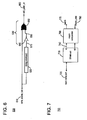
- FIG. 7 illustrates an example of a content-addressable memory (CAM) cell that may be implemented using the SRAM cell circuits disclosed above.
- CAM memory device 700 includes SRAM cell 710 and match comparator 760.
- SRAM cell 710 may be implemented, for example, by circuit 200 of Figure 2 .
- SRAM cell 710 includes a read/write port 720 implemented, for example, by access transistors 250 and 260 of circuit 200.
- a logic state and its complement stored in SRAM cell 710 are provided to match comparator 760 (e.g., as bit lines 270 and 280of circuit 200).
- Match comparator 760 compares a data value received at match-data port 780 against the value stored in SRAM cell 710.to provide an output value for match signal 770.
- the elastic power header device includes transistors and an adjustable bias to mimic a programmable resistor. Adjustment can be continuously adjustable or step-wise adjustable.
- the adjustment bias can also be either an adjustable current or an adjustable voltage, even though it will be referred to as an adjustment voltage hereafter.
- This transistor and adjustment voltage combination is utilized in an SRAM cell for read operations.
- a transistor can be held to operate at an adjustable strength such as in linear or saturation region by an adjustment voltage. This in turn varies the resistance in the transistor and allows the voltage on a power supply line to approximate a reference voltage, for instance, V dd .
- the resistance of the elastic power header device can also be made programmable. Properties of the elastic power header device may be programmed before processing, or set "on-the-fly.” This implementation improves the read margin of the SRAM cell.
- the elastic power header device includes actual programmable resistors, instead of transistors, which have resistance values that may be varied in a SRAM cell during a read. The read margin of the SRAM cell is thereby improved.
- the elastic power header device includes transistors and a logic circuit used during a write operation.
- the transistors and the logic circuit act like a switch to affect the relative resistances in split-power lines. In this manner, the write operation is optimally performed, thereby improving the write margin of the SRAM cell.
- the elastic power header device includes transistors, an adjustment voltage, and a logic circuit to be used during both a read operation and a write operation. In this manner, the elastic power header device improves both the read margin and the write margin of the SRAM cell.
- the elastic power header device splits the power supply into two power supply lines using a programmable resistor to control the effective resistances in the split power lines.
- One advantage of such an elastic power header device is improved read margin achieved by improving read stability, reducing read disturbance and improving SNM.
- the elastic power header device also improves both the read and write margin of the SRAM cell simultaneously.
- the elastic power header device in accordance with the various embodiments described herein may be used with SRAM cells providing multiple bidirectional or unidirectional read or write ports.
- a positive reference voltage 120 has been described herein, the techniques of the invention are equally applicable when applied to a negative reference voltage (e.g., ground).
- a negative reference voltage e.g., ground
- the embodiments of the invention, including the various circuits for implementing elastic power header device 180 described herein can provide reliable voltage operation ranges for the connected SRAM cells, despite possible variations in individual circuit components.
- HDL hardware description language
- Applicable HDLs include those at the layout, circuit netlist, register transfer, and/or schematic capture levels. Examples of HDLs include, but are not limited to: GDS II and OASIS (layout level); various SPICE languages, and IBIS (circuit netlist level); Verilog and VHDL (register transfer level); and Virtuoso custom design language and Design Architecture-IC custom design language (schematic capture level). HDL descriptions may also be used for a variety of purposes, including but not limited to layout, behavior, logic and circuit design verification, modeling and/or simulation.
Landscapes
- Engineering & Computer Science (AREA)
- Power Engineering (AREA)
- Microelectronics & Electronic Packaging (AREA)
- Computer Hardware Design (AREA)
- Static Random-Access Memory (AREA)
- Semiconductor Memories (AREA)
- Electronic Switches (AREA)
- Keying Circuit Devices (AREA)
- Synchronisation In Digital Transmission Systems (AREA)
- Inks, Pencil-Leads, Or Crayons (AREA)
- Electrophonic Musical Instruments (AREA)
Abstract
Description
- This application claims the benefit of
U.S. Nonprovisional Patent Application No. 11/932,967 filed on October 31, 2007 U.S. Nonprovisional Patent Application No. 11/938,196 filed on November 9, 2007 U.S. Provisional Patent Application No. 60/888,006 filed on February 2, 2007 U.S. Nonprovisional Patent Application No. 11/932,555 filed on October 31, 2007 U.S. Nonprovisional Patent Application No. 11/932,643 filed on October 31, 2007 - Static random access memory (SRAM) cells can be implemented using cross- coupled logic gates which maintain logic states representing data values. Ideally, SRAM cells should hold their stored logic states despite possible changes in voltage, temperature, or other operating conditions. Unfortunately, existing SRAM cell designs often fail to provide high degrees of read stability.
- As SRAM cell operating voltages are reduced, the internal nodes of the SRAM cell may be vulnerable to read disturbance. For example, during a read operation, the internal SRAM nodes may be inadvertently charged through the access transistors to rise above a trip voltage of the SRAM cell, thereby causing the SRAM cell to inadvertently switch logic states.
- The Static Noise Margin (SNM) is a "figure of merit" which measures read stability and read margin. See Benton H. Calhoun and Anantha Chandrakasan, Analyzing Static Noise Margin for Subthreshold SRAM in 65nm CMOS, http://www-mtl.mit.edu/researchgroups/icsystems/pubs/conferences/2005/bcalhoun_esscirc2005_pap er.pdf (September 2005). See also Evert Seevinck, Frans J. List, Jan Lohstroh, Static- Noise Margin Analysis of MOS SRAM Cells, IEEE JOURNAL OF SOLID-STATE CIRCUITS, Vol. SC-22, No. 5, pp. 748-754 (October 1987).
- Essentially, designers aim for the most symmetrical SNM curve that is possible, with the widest "eye." The "eye" is the gap between the lowest logic high and the highest logic low voltages that form the SNM curve. A symmetrical SNM curve with a wide "eye" represents strong read stability, optimal read margin, and minimal read disturbance. Conversely, an asymmetrical graph with a reduced eye represents low read stability, minimal read margin, and high read disturbance. Therefore, to improve read margin, a designer's goal is to achieve a symmetrical SNM curve with the widest eye possible.
- To minimize read disturbance, increase read stability, improve read margin, and improve the SNM, a designer can reduce the ratio between the sizes of the NMOS driver transistor and the NMOS pass transistor in a SRAM cell. However, when NMOS transistors are manufactured in a modern manufacturing process (e.g. a 65 nm process), the variation from the desired ratio between the driver and the pass transistor can be significant. For example, in NMOS transistors manufactured in a 65 nm process, the variation from the desired ratio can be as large as 10:1. These large variations lead to differences in resistance, channel length, threshold voltage, and other device characteristics. Large variations in size ratios and device characteristics are a major cause of low read stability.
- In one approach to reduce read disturbance, improve read stability, and increase read margin, an additional pair of PMOS transistors is added to the SRAM cell so that the overall ratio of the PMOS transistors to the NMOS transistors in the SRAM cell is minimized. The additional pair of PMOS transistors also makes the SNM curve symmetrical, resulting in a wider "eye." This approach tries to minimize the variation in size ratio between the NMOS driver and pass transistors by counter-balancing voltages in the SRAM cell. Although adding a pair of PMOS transistors alleviates the problem slightly, such an approach has its own drawbacks. The PMOS transistors eventually get so strong that they pull nodes in the SRAM cell high when they should not be pulled high, leading to poor read stability.
- In another approach to reduce read disturbance and improve read stability, the variations in device characteristics are reduced by a "Dual Stress Layer" in selected transistors (e.g. a pass gate transistor) of a SRAM cell. See Shou-Gwo Wuu, Jin- Yuan Lee, Dun-Nian Yaung, Jeng-Han Lee,
U.S. Patent No. 6,635,936 ("SRAM Layout for Relaxing Mechanical Stress in Shallow Trench Isolation Technology"); Mark Craig, Karsten Wieczorek, Manfred Horstmann,WO/2007/018780 ("SRAM Devices Utilizing Tensile-Stressed Strain Films"). However, this approach restricts the variations in device characteristics only from a device physics perspective. This approach does not address the larger problem of voltage and size ratio variance in a SRAM cell that leads to read instability, higher read disturbance, and a lower SNM. - As can be seen, both adding a pair of PMOS transistors and a solution aimed at altering the device characteristics of SRAM transistors are problematic.
[009A]US 7,092,280 discloses a CMOS static random access memory (SRAM) array with dynamically asymmetric cells, an integrated circuit (IC) chip including the SRAM and a method of accessing data in the SRAM. Each column of cells is connected to a pair of column supply lines supplying power to the column. During each SRAM access, a higher voltage is applied to one column supply line in each pair of the columns being accessed to unbalance cells in the columns being accessed. Unbalanced cells become asymmetric during accesses and the supply imbalance favors the data state being written/read. - [009B] The invention is defmed in the claims.
- An embodiment of the invention enables an increase read stability, decrease read disturbance, improve the SNM, and improve read margin for an SRAM memory cell. An embodiment of this invention provides a memory device that includes: a reference voltage; a first and a second power supply line; a static random access memory (SRAM) cell with cross-coupled first and second logic gates, with the first power supply line and the second power supply line respectively supplying the first and the second logic gates; and an elastic power header device provides, during a write operation of the first SRAM cell, different power levels on the first power supply line and the second power supply line and that provides, during a read operation, a programmable resistance in the first power supply line and the second power supply line.
- Further to meet this need, other embodiments of this invention provide an elastic power header device that provides a memory device with a first and second power supply lines. The elastic power device includes: (1) a first path having first and second power differences between a reference voltage and, respectively, the first and second power supply lines; (2) second and third paths that are coupled between the reference voltage and, respectively, the first and second power supply lines wherein, during a write operation, resistance in either the second path or the third path is varied to provide a power difference between the first and second power supply lines; and (3) fourth and fifth paths that are coupled between the reference voltage and, respectively, the first and second power supply lines wherein, during a read operation, a programmable resistance is provided in a selected one of the fourth path or the fifth path.
- Various embodiments of this invention include methods of operating the above or similar memory devices, and computer-readable media that use hardware description languages (HDLs) to describe the above or similar memory devices.
-
Figure 1 is a conceptual blockdiagram showing circuit 100, in which a number of SRAM cells are connected to an elastic power header device, in accordance with one embodiment of the invention. -
Figure 2 showscircuit 200, which implements an SRAM cell suitable for use as any ofSRAM cells 110 ofFigure 1 , in accordance with an embodiment of the invention. -
Figure 3 illustratescircuit 300, which implements an elastic power header device in accordance with an embodiment of the invention. -
Figure 4 illustratescircuit 400, which may be also be used to implement elasticpower header device 180 ofFigure 1 , in accordance with another embodiment of the invention. -
Figure 5 illustratescircuit 500, which implements elasticpower header device 180 ofFigure 1 , in accordance with another embodiment of the invention. -
Figure 6 showscircuit 600, which provides a low-going pulse, which may be used to provide write enablesignal 425 during a read or write operation in elasticpower header circuit 180 ofFigure 1 , in accordance with an embodiment of the invention. -
Figure 7 illustrates an example of a content-addressable memory (CAM) cell that may be implemented using the SRAM cell circuits disclosed above. - To allow cross-referencing among the figures, like elements in the figures are provided like reference numerals.
- In accordance with the present invention, an elastic power header device improves the read margin and read stability of a memory cell, such as an SRAM cell. In particular, an elastic power header device described herein acts as a programmable resistance to allow the power supply lines to reach a voltage equal to a desired reference voltage, without experiencing a threshold drop. Therefore, an elastic power header device of the present invention provides additional flexibility in both read margin and read stability. The additional flexibility may also be varied with an adjustment voltage, which can be used to fine-tune and control the read margin.
-
Figure 1 is a conceptual blockdiagram showing circuit 100, in which a number ofSRAM cells 110 are connected to elasticpower header device 180, in accordance with an embodiment of the invention. Several possible circuit implementations for elasticpower header device 180 are illustrated inFigs. 3 through 5 , as further described herein. - In
Figure 1 ,SRAM cells 110 are each connected topower supply lines SRAM cells 110 may be implemented by cross-coupled logic gates (e.g., cross-coupled inverters). Elasticpower header device 180 may also act as "split power switch" that provide voltages ofpower supply lines 60/888,006, filed on February 2, 2007 power supply lines - Elastic
power header device 180 selectively adjusts the voltages provided topower supply lines power header device 180 may be configured to provide substantially referencevoltage 120 during a read operation, while allowing the voltage of one ofpower supply lines SRAM cells 110. - Although
SRAM cells 110 are shown inFigure 1 as a single column of memory cells connected to a single split power switch 140, it is understood thatFigure 1 is merely illustrative. In a typical implementation, additional groups ofSRAM cells 110 connect topower supply lines power header devices 180 may be used to provide power to these additional groups of SRAM cells. Alternatively, the additional SRAM cells may sharepower supply lines power header device 180. Furthermore, the single column of memory cells may be split into multiple sub-columns, each sub-column having its ownpower supply lines - As also shown in
Fig. 1 ,bit lines -
Figure 2 showscircuit 200, which implements an SRAM cell that is suitable for use as any ofSRAM cells 110 ofFigure 1 , in accordance with an embodiment of the invention. As shown inFigure 2 ,circuit 200 includes cross-coupled inverters 225 and 245 implemented byPMOS transistors NMOS transistors PMOS transistor 210 connects topower supply line 135, whilePMOS transistor 230 connects topower supply line 125.NMOS transistors Figure 2 further shows that n-well and p-well voltages 205 and 215 (labeled Vnw and Vpw, respectively), each may differ from eitherreference voltage 120 orreference voltage 295. The n-well voltage 205 must be greater than or equal to the maximum ofpower supply lines well voltage 205 is not the same line as eitherpower supply lines power supply lines - Access or pass
transistors word line 290 andbit lines internal nodes circuit 200, to maintain a stored logic state, elasticpower header device 180 provides that the voltage of each ofpower supply lines reference voltage 120. During a read operation, elasticpower header device 180 maintains each ofpower supply lines reference voltage 120. During a read operation,bit lines word line 290 may then be set to a logic high voltage, so thataccess transistors nodes lines - During a write operation, to allow a logic state represented by a higher voltage ("logic high") to be establish in node 255 (relative to the voltage representing the opposite logic state ("logic low") to be established in node 265), elastic
power header device 180 permits the voltage ofpower supply line 125 to fall belowreference voltage 120, while maintaining the voltage ofpower supply line 135 at approximatelyreference voltage 120. In this example,nodes NMOS transistor 220 andPMOS transistor 230 are conducting, whilePMOS transistors 210 andNMOS transistor 240 are non-conducting. During the write operation,bit lines word line 290 is driven to logic high to turn onaccess transistors bit line 280 pullsnode 265 down from logic high to logic low. BecausePMOS transistor 230 is initially conducting, its current acts to pull up the voltage atnode 265. However, withpower supply line 125 falling belowreference voltage 120, resulting in less current flowing intransistor 230 than would otherwise flow,bit line 280 can more rapidly turn onPMOS transistor 210 which, in turn, turns onNMOS transistor 240 to pull downnode 265. By maintaining the voltage ofpower supply line 135 approximately atreference voltage 120,transistor 210 allows the voltage atnode 255 to be more rapidly pulled up. - Selectively reducing the voltage at
power supply line 125 during a write operation does not degrade the switch points of inverters 225 and 245. Even thoughPMOS transistor 230 on the side of the SRAM cell being pulled to logic low continues to operate in a linear mode (e.g., operating substantially as a resistor), the supply voltage atpower supply line 135 is not reduced. As a result, a sufficient write current is provided to turn onNMOS transistor 240 to rapidly lower the voltage of node below the switch point of the inverter to properly regenerate a newly logic state incircuit 200. - As one would learn from the above description, writing the opposite logic state (i.e., to bring
node 255 to logic low andnode 265 to logic high) may be facilitated by allowingpower supply line 135 to fall belowreference voltage 120, while maintainingpower supply line 125 at approximatelyreference voltage 120. -
Figure 3 illustratescircuit 300, which implements an elastic power header device (e.g., elasticpower header device 180 ofFigure 1 ), in accordance with an embodiment of the invention.Circuit 300 improves read margin.Circuit 300 includesresistive transistors reference voltage 120 to power supply lines 125 (labeled "levdd") and 135 (labeled "rivdd"), respectively.Transistors Figure 3 as being implemented by PMOS transistors. Adjustment voltage 345 (labeled "vref"), provided at the gate electrodes ofresistive transistors 320A and 302B, adjusts the effective resistance oftransistors - When maintained in the linear region,
resistive transistors power supply lines reference voltage 120. Within this region, theadjustment voltage 345 flexibly fine-tunes mainresistive transistors reference voltage 120 as desired, taking into consideration the current drawn by the switching SRAM cell, thereby achieving improved read margin and increased read stability.Adjustment voltage 345 may also be used effectively to improve write margin in a write operation, as illustrated byFigure 5 . -
Figure 4 illustratescircuit 400, which may be also be used to implement elasticpower header device 180 ofFigure 1 , in accordance with another embodiment of the invention.Circuit 400 improves write margin. -
Circuit 400 receiveswrite data signals 410A (labeled "blb") and 410B (labeled "bl"), and a write enable signal 425 (labeled "wyb").Signals power supply lines logic circuit 490, which includes NORgates gates transistors -
Transistors power supply lines voltage 120. Each oftransistors reference voltage 120 topower supply lines signals 410A-B and 425. - In
Figure 4 , NORgate 430A provides a logic low output value, except whenwrite data signal 410A and write enablesignal 425 are both at logic low. Similarly, NORgate 430B provides a logic low output, except when write data signal 410B and write enablesignal 425 are both at logic low. Thus, bothtransistors power supply lines signal 425 is at logic high, so thattransistors power supply lines reference voltage 120. -
Circuit 400 also includesclamper transistors Figure 4 as being implemented by NMOS transistors. As shown inFigure 4 , the gate and drain terminals ofclamper transistors voltage 120, so thatpower supply lines reference voltage 120 minus a threshold voltage. Accordingly,clamper transistors power supply lines transistors signals - If
write data signals signal 425 is at logic low), only one oftransistors gate 430A provides a logic low value to maintaintransistor 470A conducting, while switching offtransistor 470B. As a result,power supply line 125 remains at substantially referencevoltage 120, whilepower supply line 135 falls to referencevoltage 120 minus the threshold voltage oftransistor 450B. As described above, the voltage difference inpower supply lines -
Circuit 400 also includesweak keeper transistor 460 having its gate electrode controlled byreference voltage 495, which may be the ground reference in this embodiment. As a result,weak keeper transistor 460 provides a weak current flowing betweenpower supply lines power supply lines SRAM circuit 200. -
Figure 5 illustratescircuit 500, which implements elasticpower header device 180 ofFigure 1 , in accordance with another embodiment of the invention.Circuit 500 improves both read margin and write margin. As shown inFigure 5 ,circuit 500 includes, in addition to the elements ofcircuit 400 ofFigure 4 , additionalresistive transistors reference voltage 120 and a corresponding one ofpower supply lines circuits - When
adjustment voltage 495 is provided such thatresistive transistors circuit 500 behaves substantially the same ascircuit 400. Such an adjustment voltage may be provided during a write operation so that, as explained above,circuit 500 may improve write margin in the same manner ascircuit 400. However, if the adjustment voltage 545 is set so thatresistive transistors same time signals circuit 500 operates similar tocircuit 300, i.e., with the benefit of an improved read margin. Outside of the read and write operations,transistor power supply lines voltage 120 to ensure that the stored value in the SRAM cells maintain a high immunity to noise. In this manner,circuit 500 provides both improved read margin and improved write margin. -
Figure 6 showscircuit 600, which provides a low-going pulse, which may be used to provide write enable signal 425 a logic low state of sufficient duration during a read or write operation in elasticpower header circuit 180 ofFigure 1 , in accordance with an embodiment of the invention.Circuit 600 includes a delay element block 620 implemented by appropriate circuitry to delay the input signal, so that, for a brief time period, because ofinverter 640, a high-going signal transition atinput terminal 610 causesoutput terminal 660 ofNAND gate 650 to go to logic low. At other times,inverter 640 ensures thatoutput terminal 660 ofNAND gate 650 is at logic high. - Embodiments incorporating various features disclosed herein may be implemented in embedded or standalone SRAM memory devices, caches, register files, multi-port memories, translation lookaside buffers (TLBS), content-addressable memories (CAMS), ternary CAMS (TCAMS), or other appropriate devices to operate at lower voltages as compared to traditional six transistor SRAM cells. Such features can be particularly advantageous for mobile, portable, or ultra-low voltage devices in which lower supply voltages may advantageously permit longer battery life and/or use time.
-
Figure 7 illustrates an example of a content-addressable memory (CAM) cell that may be implemented using the SRAM cell circuits disclosed above. InFigure 7 ,CAM memory device 700 includesSRAM cell 710 andmatch comparator 760.SRAM cell 710 may be implemented, for example, bycircuit 200 ofFigure 2 . As shown inFigure 7 ,SRAM cell 710 includes a read/write port 720 implemented, for example, byaccess transistors circuit 200. A logic state and its complement stored inSRAM cell 710 are provided to match comparator 760 (e.g., asbit lines 270 and 280of circuit 200).Match comparator 760 compares a data value received at match-data port 780 against the value stored in SRAM cell 710.to provide an output value formatch signal 770. - In one embodiment of the invention, the elastic power header device includes transistors and an adjustable bias to mimic a programmable resistor. Adjustment can be continuously adjustable or step-wise adjustable. The adjustment bias can also be either an adjustable current or an adjustable voltage, even though it will be referred to as an adjustment voltage hereafter. This transistor and adjustment voltage combination is utilized in an SRAM cell for read operations. A transistor can be held to operate at an adjustable strength such as in linear or saturation region by an adjustment voltage. This in turn varies the resistance in the transistor and allows the voltage on a power supply line to approximate a reference voltage, for instance, Vdd. The resistance of the elastic power header device can also be made programmable. Properties of the elastic power header device may be programmed before processing, or set "on-the-fly." This implementation improves the read margin of the SRAM cell.
- In another embodiment, the elastic power header device includes actual programmable resistors, instead of transistors, which have resistance values that may be varied in a SRAM cell during a read. The read margin of the SRAM cell is thereby improved.
- In another embodiment, the elastic power header device includes transistors and a logic circuit used during a write operation. The transistors and the logic circuit act like a switch to affect the relative resistances in split-power lines. In this manner, the write operation is optimally performed, thereby improving the write margin of the SRAM cell.
- In another embodiment of the present invention, the elastic power header device includes transistors, an adjustment voltage, and a logic circuit to be used during both a read operation and a write operation. In this manner, the elastic power header device improves both the read margin and the write margin of the SRAM cell.
- According to another embodiment of the invention, the elastic power header device splits the power supply into two power supply lines using a programmable resistor to control the effective resistances in the split power lines. One advantage of such an elastic power header device is improved read margin achieved by improving read stability, reducing read disturbance and improving SNM. The elastic power header device also improves both the read and write margin of the SRAM cell simultaneously.
- Additional embodiments of the invention provide elastic power header devices in other devices, such as flash memories, to the extent that this invention helps with problems seen in practice. These and other features and advantages of the invention will be more readily apparent from the detailed description of the embodiments set forth below taken in conjunction with the accompanying drawings.
- The elastic power header device in accordance with the various embodiments described herein may be used with SRAM cells providing multiple bidirectional or unidirectional read or write ports. In addition, although a
positive reference voltage 120 has been described herein, the techniques of the invention are equally applicable when applied to a negative reference voltage (e.g., ground). Advantageously, the embodiments of the invention, including the various circuits for implementing elasticpower header device 180 described herein can provide reliable voltage operation ranges for the connected SRAM cells, despite possible variations in individual circuit components. - As known by one of ordinary skill in the art, this invention, including any logic circuit or transistor circuit, may be modeled, generated, or both by computer based on a description of the hardware expressed in the syntax and the semantics of a hardware description language (HDL). Such HDL descriptions are often stored on a computer readable medium. Applicable HDLs include those at the layout, circuit netlist, register transfer, and/or schematic capture levels. Examples of HDLs include, but are not limited to: GDS II and OASIS (layout level); various SPICE languages, and IBIS (circuit netlist level); Verilog and VHDL (register transfer level); and Virtuoso custom design language and Design Architecture-IC custom design language (schematic capture level). HDL descriptions may also be used for a variety of purposes, including but not limited to layout, behavior, logic and circuit design verification, modeling and/or simulation.
- Aspects of the subject matter described herein are set out in the following numbered clauses:
- 1. A memory device comprising:
- a first power supply line;
- a second power supply line;
a static random access memory (SRAM) cell comprising a first logic gate and a second logic gate that are cross-coupled, wherein the first power supply line supplies the first logic gate, and the second power supply line supplies the second logic gate; and - an elastic power header device connected between a reference voltage and each one of the first power supply line and the second power supply line wherein the elastic power header device is configured to provide, during a write operation of the first SRAM cell, different power supply levels on the first power supply line and the second power supply line and is configured to provide, during a read operation, a first resistance in the first power supply line and a second resistance in the second power supply line.
- 2. The memory device of clause 1, wherein at least one of the first and second resistances comprise a programmable resistance.
- 3. The memory device of clause 1 wherein, during the write operation, the first power supply line has a different voltage level than the second power supply line.
- 4. The memory device of clause 1 wherein, during the write operation, the first power supply line has a different current flow than the second power supply line.
- 5. The memory device of clause 1 wherein, during the write operation, which of the first and the second power supply lines has a higher power supply level is determined by the value of the data bit being written.
- 6. The memory device of clause 1 wherein, during the read operation, the first resistance and the second resistance are substantially equal, whereby a difference in power supply levels between the first power supply line and the second power supply line depends on the current drawn from each power supply line.
- 7. The memory device of clause 1 wherein, during the write operation, the different power supply levels are provided by a variable resistance in a selected one of the power supply lines to facilitate writing into the first SRAM cell.
- 8. The memory device of clause 1, wherein the different power supply levels between the first power supply line and the second power supply line during the write operation corresponds to a threshold voltage drop across a transistor.
- 9. The memory device of clause 1, further comprising a keeper circuit for limiting the difference between the first power supply line and the second power supply line.
- 10. The memory device of clause 1, wherein the memory device is configured for use in at least one of: an embedded SRAM memory device, a standalone SRAM memory device, a cache, a register file, a multi-port memory, a translation lookaside buffer, a content-addressable memory, or a ternary content-addressable memory.
- 11. A memory device comprising:
- a first power supply line;
- a second power supply line;
- a static random access memory (SRAM) cell comprising a first logic gate and a second logic gate that are cross-coupled, wherein the first power supply line supplies the first logic gate, and the second power supply line supplies the second logic gate; and
- an elastic power header device connected between a reference voltage and each one of the first power supply line and the second power supply line wherein the elastic power header device is configured to provide, during a read operation, a first resistance in the first power supply line and a second resistance in the second power supply line.
- 12. The memory device of clause 11, wherein at least one of the first and second resistances comprise a transistor.
- 13. A method for achieving improved read and write margins in a memory device comprising a first power supply line, a second power supply line, and a first logic gate and a second logic gate that are cross-coupled, the method comprising:
- maintaining, during a read operation of the memory device, a resistance in each one of the first power supply line and the second power supply line to provide a power supply level greater than a predetermined value; and
- varying, during a write operation of the memory device, a resistance in a selected one of the first power supply line and the second power supply line to provide a power supply level difference between the first power supply line and the second power supply line.
- 14. The method of clause 13, wherein the resistance comprises a programmable resistance.
- 15. The method of clause 13, wherein the power supply level comprises a voltage.
- 16. The method of clause 13, wherein the power supply level comprises a current,
- 17. The method of clause 13, further comprising varying a conductance of a transistor connected between a reference voltage and the selected one of the first power supply line and the second power supply line.
- 18. The method of clause 13, further comprising equalizing the first power supply line and the second power supply line at a time when neither of the read or the write operations is occurring.
- 19. A method for achieving improved read margin in a memory device comprising a first power supply line, a second power supply line, and a first logic gate and a second logic gate that are cross-coupled, the method comprising:
- maintaining, during a read operation of the memory device, a resistance in each one of the first power supply line and the second power supply line; and
- providing a power supply level to a selected one of the first power supply line and the second power supply line greater than a predetermined value.
- 20. The method of clause 19, further comprising controlling a device configured to achieve a resistance.
- 21. An elastic power header device for providing a first power supply line and a second power supply line in a split power fashion to a memory device, comprising:
- a first conductive path, coupled between a reference voltage and both the first power supply line and the second power supply line, configured to provide a first power supply level difference between the reference voltage and each one of the first power supply line and the second power supply line;
- a second conductive path, coupled between the reference voltage and the first power supply line;
- a third conductive path, coupled between the reference voltage and the second power supply line, wherein, in response to a read operation, a resistance in a selected one of the second conductive path or the third conductive path is kept within a predetermined range of values during a write operation to provide a power supply level difference between the first power supply line and the second power supply line;
- a fourth conductive path, coupled between the reference voltage and the first power supply line; and
- a fifth conductive path, coupled between the reference voltage and the second power supply line wherein, in response to a write operation, the resistance in a selected one of the fourth and the fifth conductive paths is varied to provide a resistance.
- 22. The elastic power header device of clause 21, wherein the resistance comprises a programmable resistance.
- 23. The elastic power header device of clause 21, wherein the first to fifth conductive paths each comprise a transistor.
- 24. The elastic power header device of clause 21, wherein the fourth and fifth conductive paths are attenuated during a write operation.
- 25. The elastic power header device of clause 21, wherein the second and the third conductive paths are attenuated during a read operation.
- 26. An elastic power header device for providing a first power supply line and a second power supply line in a split power fashion to a memory device, comprising:
- a first conductive path coupled between the reference voltage and the first power supply line; and
- a second conductive path coupled between the reference voltage and the second power supply line; wherein, in response to a read operation, the relative resistance between the first conductive path and the second conductive path is kept within a predetermined range of values.
- 27. A computer-readable medium that includes a description of a circuit that implements an elastic power header device which includes a first power supply line and a second power supply line organized in a split power fashion in a memory device, where the circuit is adapted for use with a processor that executes operations that represent instructions, the instructions comprising:
- configuring a first conductive path coupled between a reference voltage and both the first power supply line and the second power supply line, configured to provide a first voltage between the reference voltage and each one of the first power supply line and the second power supply line;
- configuring a second conductive path, coupled between the reference voltage and the first power supply line;
- configuring a third conductive path, coupled between the reference voltage and the second power supply line, wherein, in response to a read operation, a resistance in a selected one of the second conductive path or the third conductive path is kept within a predetermined range of values during a write operation to provide a power supply level difference between the first power supply line and the second power supply line;
- configuring a fourth conductive path, coupled between the reference voltage and the first power supply line to provide a resistance in the first power supply line in response to a write operation; and
- configuring a fifth conductive path, coupled between the reference voltage and the second power supply line to provide the resistance in the second power supply line in response to a write operation.
- 28. The computer-readable medium as in clause 27, wherein the first to fifth conductive paths each comprise a device controlled to operate at an adjustable strength during a read operation.
- 29. A computer-readable medium that includes a description of a circuit that implements an elastic power header device which includes a first power supply line and a second power supply line organized in a split power fashion in a memory device, where the circuit is adapted for use with a processor that executes operations that represent instructions, the instructions comprising:
- a first conductive path coupled between the reference voltage and the first power supply line; and
- a second conductive path coupled between the reference voltage and the second power supply line;
- wherein, in response to a read operation, the relative resistance between the first conductive path and the second conductive path is kept within a predetermined range of values.
- 30. The computer-readable medium as in clause 29, wherein the first to fifth conductive paths each comprise a device controlled to operate at an adjustable strength during a read operation.
- 31. A computer readable medium that includes a description of a memory device, where the memory device comprises:
- a first power supply line;
- a second power supply line;
- a static random access memory (SRAM) cell comprising a first logic gate and a second logic gate that are cross-coupled, wherein the first power supply line supplies the first logic gate, and the second power supply line supplies the second logic gate; and
- an elastic power header device connected between the reference voltage and each one of the first power supply line and the second power supply line wherein the elastic power header device is configured to provide, during a write operation of the first SRAM cell, different power supply levels on the first power supply line and the second power supply line and is configured to provide, during a read operation, a first resistance in the first power supply line and a second resistance in the second power supply line.
- 32. The computer-readable medium as in clause 31, wherein at least one of the first and second resistances comprise a programmable resistance.
- 33. A computer-readable medium that includes a description of a memory device, where the memory device comprises:
- a first power supply line;
- a second power supply line;
- a static random access memory (SRAM) cell comprising a first logic gate and a second logic gate that are cross-coupled, wherein the first power supply line supplies the first logic gate, and the second power supply line supplies the second logic gate; and
- an elastic power header device connected between the reference voltage and each one of the first power supply line and the second power supply line wherein the elastic power header device is configured to provide, during a read operation, a first resistance in the first power supply line and a second resistance in the second power supply line.
- 34. The computer-readable medium as in clause 33, wherein at least one of the first and second resistances comprise a programmable resistance.
- 35. A memory device comprising:
- means for providing a reference voltage;
- means for configuring a first power supply line and a second power supply line, and means for connecting a static random access memory (SRAM) cell comprising a first logic gate and a second logic gate that are cross-coupled, wherein the first power supply line supplies the first logic gate, and the second power supply line supplies the second logic gates; and
- means for providing elastic power connected between the reference voltage and each one of the first power supply line and the second power supply line providing, during a write operation of the first SRAM cell, different power supply levels on the first power supply line and the second power supply line and, during a read operation, providing a first resistance in the first power supply line and a second resistance in the second power supply line.
- 36. A memory device comprising:
- means for providing a reference voltage;
- means for configuring a first power supply line and a second power supply line, and means for connecting a static random access memory (SRAM) cell comprising a first logic gate and a second logic gate that are cross-coupled, wherein the first power supply line supplies the first logic gate, and the second power supply line supplies the second logic gate; and
- means for providing elastic power connected between the reference voltage and each one of the first power supply line and the second power supply line providing, during a read operation, a first resistance in the first power supply line and a second resistance in the second power supply line.
- The foregoing disclosure is not intended to limit the invention to the precise forms or particular fields of use disclosed. Various alternate embodiments, variations or modifications to the invention are possible within the scope of the invention in light of the disclosure. The invention is set forth in the following claims.
Claims (13)
- A memory device comprising:a first power supply line (125);a second power supply line (135);a static random access memory -SRAM- cell (110) comprising a first logic gate (230) and a second logic gate (210) that are cross-coupled, wherein the first power supply line supplies the first logic gate, and the second power supply line supplies the second logic gate; anda power header device (180; 400; 500) configured to selectively vary power supply levels, the power header device being connected between a reference voltage (120) and each one of the first power supply line and the second power supply line,wherein the power header device is configured to provide, during a write operation of the SRAM cell, different power supply levels on the first power supply line and the second power supply line, characterized in that the power header device is configured to provide, during a read operation, a first resistance (470A) in the first power supply line and a second resistance (470B) in the second power supply line, the first and second resistances being substantially equal; andwherein the power header device comprises a logic circuit (490) configured to receive one or more write data signals (410A, 410B) and a write enable signal (425) and to provide an output dependent on the levels of the write data signal(s) and the write enable signal for selectively varying the power supply levels on the first supply line and the second power supply line.
- The memory device of claim 1, wherein at least one of the first and second resistances comprise a programmable resistance.
- The memory device of claim 1, wherein, during the write operation, the first power supply line has at least one of a different voltage level than the second power supply line or a different current flow than the second power supply line.
- The memory device of claim 1, wherein, during the write operation, which of the first and the second power supply lines has a higher power supply level is determined by the value of the data bit being written.
- The memory device of claim 1, wherein, during the read operation, a difference in power supply levels between the first power supply line and the second power supply line depends on the current drawn from each power supply line.
- The memory device of claim 1, wherein, during the write operation, the different power supply levels are provided by a variable resistance in a selected one of the power supply lines to facilitate writing into the first SRAM cell.
- The memory device of claim 1, wherein the different power supply levels between the first power supply line and the second power supply line during the write operation corresponds to a threshold voltage drop across a transistor.
- The memory device of claim 1, further comprising a keeper circuit for limiting the difference between the first power supply line and the second power supply line.
- The memory device of claim 1, wherein the memory device is configured for use in at least one of: an embedded SRAM memory device, a standalone SRAM memory device, a cache, a register file, a multi-port memory, a translation lookaside buffer, a content-addressable memory, or a ternary content-addressable memory.
- The memory device of claim 1, wherein at least one of the first and second resistances comprise a transistor.
- The memory device of claim 1, wherein comprises:a first conductive path, coupled between a reference voltage and both the first power supply line and the second power supply line, configured to provide the first power supply level difference between the reference voltage and each one of the first power supply line and the second power supply line;a second conductive path, coupled between the reference voltage and the first power supply line;a third conductive path, coupled between the reference voltage and the second power supply line, wherein, in response to a read operation, a resistance in a selected one of the second conductive path or the third conductive path is kept within a predetermined range of values during a write operation to provide a power supply level difference between the first power supply line and the second power supply line;a fourth conductive path, coupled between the reference voltage and the first power supply line; anda fifth conductive path, coupled between the reference voltage and the second power supply line wherein, in response to a write operation, the resistance in a selected one of the fourth and the fifth conductive paths is varied to provide a resistance.
- The memory device of claim 1, wherein the power header device comprises:a first conductive path coupled between the reference voltage and the first power supply line; anda second conductive path coupled between the reference voltage and the second power supply line; wherein, in response to a read operation, the relative resistance between the first conductive path and the second conductive path is kept within a predetermined range of values.
- A method for achieving improved read margin in the memory device of any one of claims 1 to 12, the method comprising:maintaining, during a read operation of the memory device, a substantially equal resistance in each one of the first power supply line and the second power supply line to provide a power supply level greater than a predetermined value; andvarying, during a write operation of the memory device, a resistance in a selected one of the first power supply line and the second power supply line to provide a power supply level difference between the first power supply line and the second power supply line, wherein the varying comprises:receiving a write data signal and a write enable signal at the logic circuit; andthe logic circuit selectively providing an output for varying the power supply levels on the first power supply line and on the second power supply line based on upon the levels of the write data signal and the write enable signal.
Applications Claiming Priority (6)
| Application Number | Priority Date | Filing Date | Title |
|---|---|---|---|
| US88800607P | 2007-02-02 | 2007-02-02 | |
| US11/932,555 US7952910B2 (en) | 2007-02-02 | 2007-10-31 | Memory device with split power switch |
| US11/932,967 US7672187B2 (en) | 2007-02-02 | 2007-10-31 | Elastic power for read and write margins |
| US11/932,643 US20080266995A1 (en) | 2007-02-02 | 2007-10-31 | Method of selectively powering memory device |
| US11/938,196 US7869263B2 (en) | 2007-02-02 | 2007-11-09 | Elastic power for read margin |
| PCT/US2008/052496 WO2008097783A2 (en) | 2007-02-02 | 2008-01-30 | Elastic power for read and write margins |
Publications (3)
| Publication Number | Publication Date |
|---|---|
| EP2118900A2 EP2118900A2 (en) | 2009-11-18 |
| EP2118900A4 EP2118900A4 (en) | 2010-04-21 |
| EP2118900B1 true EP2118900B1 (en) | 2011-08-17 |
Family
ID=39676026
Family Applications (2)
| Application Number | Title | Priority Date | Filing Date |
|---|---|---|---|
| EP08728581.3A Active EP2118717B1 (en) | 2007-02-02 | 2008-01-30 | Memory device with split power switch and related methods |
| EP08728583A Active EP2118900B1 (en) | 2007-02-02 | 2008-01-30 | Sram with elastic power supply for improved read and write margins |
Family Applications Before (1)
| Application Number | Title | Priority Date | Filing Date |
|---|---|---|---|
| EP08728581.3A Active EP2118717B1 (en) | 2007-02-02 | 2008-01-30 | Memory device with split power switch and related methods |
Country Status (5)
| Country | Link |
|---|---|
| US (4) | US7952910B2 (en) |
| EP (2) | EP2118717B1 (en) |
| AT (1) | ATE521067T1 (en) |
| TW (2) | TWI394173B (en) |
| WO (2) | WO2008097783A2 (en) |
Families Citing this family (24)
| Publication number | Priority date | Publication date | Assignee | Title |
|---|---|---|---|---|
| JP2007193928A (en) * | 2005-12-19 | 2007-08-02 | Matsushita Electric Ind Co Ltd | Semiconductor memory device |
| US7570537B2 (en) * | 2007-07-12 | 2009-08-04 | Sun Microsystems, Inc. | Memory cells with power switch circuit for improved low voltage operation |
| TWI399748B (en) * | 2009-01-15 | 2013-06-21 | Univ Hsiuping Sci & Tech | Dual port sram having a lower power voltage in writing operation |
| KR101034616B1 (en) * | 2009-11-30 | 2011-05-12 | 주식회사 하이닉스반도체 | Sense Amplifiers and Semiconductor Memory Devices |
| US8320203B2 (en) * | 2010-03-26 | 2012-11-27 | Intel Corporation | Method and system to lower the minimum operating voltage of register files |
| JP2012038401A (en) | 2010-08-11 | 2012-02-23 | Elpida Memory Inc | Semiconductor device and power supply control method for semiconductor device |
| US8427896B1 (en) | 2011-11-15 | 2013-04-23 | International Business Machines Corporation | Dynamic wordline assist scheme to improve performance tradeoff in SRAM |
| US8729908B2 (en) | 2012-02-29 | 2014-05-20 | International Business Machines Corporation | Static noise margin monitoring circuit and method |
| TWI494945B (en) * | 2012-03-29 | 2015-08-01 | Nat Univ Chung Cheng | Single-ended read random access memory device |
| US9317087B2 (en) * | 2012-04-26 | 2016-04-19 | Ravindraraj Ramaraju | Memory column drowsy control |
| US9019751B2 (en) | 2013-03-01 | 2015-04-28 | Qualcomm Incorporated | Process tolerant circuits |
| US9627038B2 (en) * | 2013-03-15 | 2017-04-18 | Intel Corporation | Multiport memory cell having improved density area |
| TWI562163B (en) * | 2013-07-04 | 2016-12-11 | United Microelectronics Corp | Memory cell array |
| US9105355B2 (en) * | 2013-07-04 | 2015-08-11 | United Microelectronics Corporation | Memory cell array operated with multiple operation voltage |
| TWI528361B (en) * | 2013-12-10 | 2016-04-01 | 智原科技股份有限公司 | Static memory cell |
| US9595307B2 (en) | 2014-05-22 | 2017-03-14 | Samsung Electronics Co., Ltd. | Volatile memory device and system-on-chip including the same |
| US9570155B2 (en) | 2015-06-09 | 2017-02-14 | Globalfoundries Inc. | Circuit to improve SRAM stability |
| US10049724B2 (en) * | 2016-06-07 | 2018-08-14 | Intel Corporation | Aging tolerant register file |
| US9922701B2 (en) * | 2016-08-08 | 2018-03-20 | Taiwan Semiconductor Manufacturing Company Limited | Pre-charging bit lines through charge-sharing |
| US10236036B2 (en) * | 2017-05-09 | 2019-03-19 | Micron Technology, Inc. | Sense amplifier signal boost |
| US11133039B2 (en) * | 2018-10-12 | 2021-09-28 | Taiwan Semiconductor Manufacturing Company, Ltd. | Power switch control in a memory device |
| US11967365B2 (en) * | 2019-06-11 | 2024-04-23 | Arm Limited | Bitcell architecture with time-multiplexed ports |
| US12482520B2 (en) * | 2022-11-23 | 2025-11-25 | The Trustees Of Columbia University In The City Of New York | 6T-SRAM-based digital computing-in-memory circuits supporting flexible input dimension |
| KR20240111461A (en) | 2023-01-10 | 2024-07-17 | 삼성전자주식회사 | Memory cell array of static random access memory and static random access memory including the same |
Family Cites Families (23)
| Publication number | Priority date | Publication date | Assignee | Title |
|---|---|---|---|---|
| US4686391A (en) | 1986-05-08 | 1987-08-11 | Genrad, Inc. | Fast-acting comparison circuit |
| JPH07111824B2 (en) * | 1986-12-15 | 1995-11-29 | 株式会社東芝 | Semiconductor memory |
| KR0136074B1 (en) * | 1992-09-11 | 1998-06-01 | 세키자와 스토무 | MOS-type SRAM with improved soft error resistance, high potential supply voltage drop detection circuit, complementary signal transition detection circuit and semiconductor device with improved internal signal time margin |
| US5870331A (en) | 1997-09-26 | 1999-02-09 | Advanced Micro Devices, Inc. | Application-specific SRAM memory cell for low voltage, high speed operation |
| JP3183245B2 (en) * | 1998-03-06 | 2001-07-09 | 日本電気株式会社 | Semiconductor storage device |
| US6117722A (en) * | 1999-02-18 | 2000-09-12 | Taiwan Semiconductor Manufacturing Company | SRAM layout for relaxing mechanical stress in shallow trench isolation technology and method of manufacture thereof |
| KR100346832B1 (en) * | 2000-01-12 | 2002-08-03 | 삼성전자 주식회사 | Static random access memory device and manufacturing method thereof |
| US6801994B2 (en) * | 2000-12-20 | 2004-10-05 | Microsoft Corporation | Software management systems and methods for automotive computing devices |
| JP2003045187A (en) * | 2001-08-02 | 2003-02-14 | Mitsubishi Electric Corp | Semiconductor storage device |
| JP4030383B2 (en) | 2002-08-26 | 2008-01-09 | 株式会社ルネサステクノロジ | Semiconductor device and manufacturing method thereof |
| US6771095B1 (en) * | 2002-11-22 | 2004-08-03 | Analog Devices, Inc. | Level translating digital switch |
| JP3906166B2 (en) * | 2003-02-25 | 2007-04-18 | 株式会社東芝 | Semiconductor memory device |
| JP2004362695A (en) * | 2003-06-05 | 2004-12-24 | Renesas Technology Corp | Semiconductor storage |
| US7165165B2 (en) * | 2004-03-16 | 2007-01-16 | Intel Corporation | Anticipatory power control of memory |
| US7129765B2 (en) * | 2004-04-30 | 2006-10-31 | Xilinx, Inc. | Differential clock tree in an integrated circuit |
| US7092280B2 (en) * | 2004-11-22 | 2006-08-15 | International Business Machines Corp. | SRAM with dynamically asymmetric cell |
| JP4912016B2 (en) * | 2005-05-23 | 2012-04-04 | ルネサスエレクトロニクス株式会社 | Semiconductor memory device |
| US7403426B2 (en) | 2005-05-25 | 2008-07-22 | Intel Corporation | Memory with dynamically adjustable supply |
| US7060549B1 (en) | 2005-07-01 | 2006-06-13 | Advanced Micro Devices, Inc. | SRAM devices utilizing tensile-stressed strain films and methods for fabricating the same |
| JP5100035B2 (en) | 2005-08-02 | 2012-12-19 | ルネサスエレクトロニクス株式会社 | Semiconductor memory device |
| JP4929668B2 (en) * | 2005-10-12 | 2012-05-09 | 富士通セミコンダクター株式会社 | Semiconductor memory |
| US7376001B2 (en) * | 2005-10-13 | 2008-05-20 | International Business Machines Corporation | Row circuit ring oscillator method for evaluating memory cell performance |
| JP2007193928A (en) * | 2005-12-19 | 2007-08-02 | Matsushita Electric Ind Co Ltd | Semiconductor memory device |
-
2007
- 2007-10-31 US US11/932,555 patent/US7952910B2/en active Active
- 2007-10-31 US US11/932,643 patent/US20080266995A1/en not_active Abandoned
- 2007-10-31 US US11/932,967 patent/US7672187B2/en active Active
- 2007-11-09 US US11/938,196 patent/US7869263B2/en active Active
-
2008
- 2008-01-30 WO PCT/US2008/052496 patent/WO2008097783A2/en not_active Ceased
- 2008-01-30 WO PCT/US2008/052493 patent/WO2008097782A1/en not_active Ceased
- 2008-01-30 AT AT08728583T patent/ATE521067T1/en not_active IP Right Cessation
- 2008-01-30 EP EP08728581.3A patent/EP2118717B1/en active Active
- 2008-01-30 EP EP08728583A patent/EP2118900B1/en active Active
- 2008-02-01 TW TW097103973A patent/TWI394173B/en active
- 2008-02-01 TW TW097103958A patent/TWI389130B/en active
Also Published As
| Publication number | Publication date |
|---|---|
| TW200849271A (en) | 2008-12-16 |
| US20080186791A1 (en) | 2008-08-07 |
| EP2118717B1 (en) | 2013-08-21 |
| US7869263B2 (en) | 2011-01-11 |
| EP2118717A1 (en) | 2009-11-18 |
| ATE521067T1 (en) | 2011-09-15 |
| US20080273412A1 (en) | 2008-11-06 |
| US20080186795A1 (en) | 2008-08-07 |
| US7672187B2 (en) | 2010-03-02 |
| WO2008097783A2 (en) | 2008-08-14 |
| TW200847178A (en) | 2008-12-01 |
| TWI394173B (en) | 2013-04-21 |
| TWI389130B (en) | 2013-03-11 |
| US7952910B2 (en) | 2011-05-31 |
| WO2008097783A3 (en) | 2008-10-23 |
| US20080266995A1 (en) | 2008-10-30 |
| EP2118717A4 (en) | 2010-04-07 |
| EP2118900A4 (en) | 2010-04-21 |
| EP2118900A2 (en) | 2009-11-18 |
| WO2008097782A1 (en) | 2008-08-14 |
Similar Documents
| Publication | Publication Date | Title |
|---|---|---|
| US7672187B2 (en) | Elastic power for read and write margins | |
| US7872935B2 (en) | Memory cells with power switch circuit for improved low voltage operation | |
| Wang et al. | Sub-threshold design for ultra low-power systems | |
| TWI259939B (en) | A power gating structure with concurrent data retention and intermediate modes | |
| KR101601827B1 (en) | Improved low voltage write speed bitcell | |
| US9111606B2 (en) | Tracking bit cell | |
| US9349437B2 (en) | Memory cell having built-in read and write assist | |
| JP2005117037A (en) | Method of improving cache capacity of soi and bulk | |
| TWI700706B (en) | Memory device | |
| Yabuuchi et al. | 13.3 20nm High-density single-port and dual-port SRAMs with wordline-voltage-adjustment system for read/write assists | |
| JP2010272190A (en) | Semiconductor memory device | |
| US20090129191A1 (en) | Structure for SRAM voltage control for improved operational margins | |
| US20070211517A1 (en) | System and method for operating a memory circuit | |
| KR101705172B1 (en) | Semiconductor Memory Device | |
| US10482950B2 (en) | Static random access memory devices including a plurality of storage cells and a read/write circuit | |
| Mishra et al. | Static noise margin and power dissipation analysis of various SRAM topologies | |
| US7626853B1 (en) | Method of operating memory cell providing internal power switching | |
| Dhindsa et al. | A novel differential 9T cell SRAM with reduced sub threshold leakage power | |
| Zanjani et al. | A new subthreshold half-select free SRAM with dynamic feedback cut-off for low-power and high speed applications | |
| CN201910251U (en) | Memory unit circuit with self-adaptive leakage current cutting-off mechanism | |
| Karthika et al. | Power analysis of bit interleaving 9T SRAM array | |
| Tawfik et al. | Stability enhancement techniques for nanoscale SRAM circuits: A comparison | |
| Gomase et al. | Stability analysis of SRAM cell for energy reduction using deep sub micron technology | |
| Abu-Rahma et al. | Variation-Tolerant SRAM Write and Read Assist Techniques | |
| TW200419575A (en) | Low-power high-performance storage circuitry and related methods |
Legal Events
| Date | Code | Title | Description |
|---|---|---|---|
| PUAI | Public reference made under article 153(3) epc to a published international application that has entered the european phase |
Free format text: ORIGINAL CODE: 0009012 |
|
| 17P | Request for examination filed |
Effective date: 20090828 |
|
| AK | Designated contracting states |
Kind code of ref document: A2 Designated state(s): AT BE BG CH CY CZ DE DK EE ES FI FR GB GR HR HU IE IS IT LI LT LU LV MC MT NL NO PL PT RO SE SI SK TR |
|
| RIN1 | Information on inventor provided before grant (corrected) |
Inventor name: WENDELL, DENNIS Inventor name: LIU, JUN Inventor name: FUNG, DANIEL Inventor name: BHATIA, AJAY Inventor name: LIH, YOLIN Inventor name: BALASUBRAMANIAN, SHYAM |
|
| A4 | Supplementary search report drawn up and despatched |
Effective date: 20100318 |
|
| RIC1 | Information provided on ipc code assigned before grant |
Ipc: G11C 11/419 20060101AFI20100312BHEP |
|
| DAX | Request for extension of the european patent (deleted) | ||
| RIC1 | Information provided on ipc code assigned before grant |
Ipc: G11C 11/419 20060101AFI20110106BHEP |
|
| RTI1 | Title (correction) |
Free format text: SRAM WITH ELASTIC POWER SUPPLY FOR IMPROVED READ AND WRITE MARGINS |
|
| GRAP | Despatch of communication of intention to grant a patent |
Free format text: ORIGINAL CODE: EPIDOSNIGR1 |
|
| GRAS | Grant fee paid |
Free format text: ORIGINAL CODE: EPIDOSNIGR3 |
|
| GRAA | (expected) grant |
Free format text: ORIGINAL CODE: 0009210 |
|
| AK | Designated contracting states |
Kind code of ref document: B1 Designated state(s): AT BE BG CH CY CZ DE DK EE ES FI FR GB GR HR HU IE IS IT LI LT LU LV MC MT NL NO PL PT RO SE SI SK TR |
|
| REG | Reference to a national code |
Ref country code: GB Ref legal event code: FG4D |
|
| REG | Reference to a national code |
Ref country code: CH Ref legal event code: EP |
|
| REG | Reference to a national code |
Ref country code: IE Ref legal event code: FG4D |
|
| REG | Reference to a national code |
Ref country code: DE Ref legal event code: R096 Ref document number: 602008008946 Country of ref document: DE Effective date: 20111020 |
|
| RAP2 | Party data changed (patent owner data changed or rights of a patent transferred) |
Owner name: ORACLE AMERICA, INC. |
|
| REG | Reference to a national code |
Ref country code: NL Ref legal event code: VDEP Effective date: 20110817 Ref country code: GB Ref legal event code: 732E Free format text: REGISTERED BETWEEN 20111110 AND 20111116 |
|
| REG | Reference to a national code |
Ref country code: DE Ref legal event code: R082 Ref document number: 602008008946 Country of ref document: DE Representative=s name: WSL PATENTANWAELTE PARTNERSCHAFT MBB, DE Effective date: 20111020 Ref country code: DE Ref legal event code: R081 Ref document number: 602008008946 Country of ref document: DE Owner name: ORACLE AMERICA, INC., REDWOOD CITY, US Free format text: FORMER OWNER: MONTALVO SYSTEMS, INC., SANTA CLARA, CALIF., US Effective date: 20111020 |
|
| LTIE | Lt: invalidation of european patent or patent extension |
Effective date: 20110817 |
|
| PG25 | Lapsed in a contracting state [announced via postgrant information from national office to epo] |
Ref country code: NO Free format text: LAPSE BECAUSE OF FAILURE TO SUBMIT A TRANSLATION OF THE DESCRIPTION OR TO PAY THE FEE WITHIN THE PRESCRIBED TIME-LIMIT Effective date: 20111117 Ref country code: FI Free format text: LAPSE BECAUSE OF FAILURE TO SUBMIT A TRANSLATION OF THE DESCRIPTION OR TO PAY THE FEE WITHIN THE PRESCRIBED TIME-LIMIT Effective date: 20110817 Ref country code: LT Free format text: LAPSE BECAUSE OF FAILURE TO SUBMIT A TRANSLATION OF THE DESCRIPTION OR TO PAY THE FEE WITHIN THE PRESCRIBED TIME-LIMIT Effective date: 20110817 Ref country code: SE Free format text: LAPSE BECAUSE OF FAILURE TO SUBMIT A TRANSLATION OF THE DESCRIPTION OR TO PAY THE FEE WITHIN THE PRESCRIBED TIME-LIMIT Effective date: 20110817 Ref country code: IS Free format text: LAPSE BECAUSE OF FAILURE TO SUBMIT A TRANSLATION OF THE DESCRIPTION OR TO PAY THE FEE WITHIN THE PRESCRIBED TIME-LIMIT Effective date: 20111217 Ref country code: NL Free format text: LAPSE BECAUSE OF FAILURE TO SUBMIT A TRANSLATION OF THE DESCRIPTION OR TO PAY THE FEE WITHIN THE PRESCRIBED TIME-LIMIT Effective date: 20110817 Ref country code: PT Free format text: LAPSE BECAUSE OF FAILURE TO SUBMIT A TRANSLATION OF THE DESCRIPTION OR TO PAY THE FEE WITHIN THE PRESCRIBED TIME-LIMIT Effective date: 20111219 |
|
| REG | Reference to a national code |
Ref country code: AT Ref legal event code: MK05 Ref document number: 521067 Country of ref document: AT Kind code of ref document: T Effective date: 20110817 |
|
| PG25 | Lapsed in a contracting state [announced via postgrant information from national office to epo] |
Ref country code: GR Free format text: LAPSE BECAUSE OF FAILURE TO SUBMIT A TRANSLATION OF THE DESCRIPTION OR TO PAY THE FEE WITHIN THE PRESCRIBED TIME-LIMIT Effective date: 20111118 Ref country code: CY Free format text: LAPSE BECAUSE OF FAILURE TO SUBMIT A TRANSLATION OF THE DESCRIPTION OR TO PAY THE FEE WITHIN THE PRESCRIBED TIME-LIMIT Effective date: 20110817 Ref country code: PL Free format text: LAPSE BECAUSE OF FAILURE TO SUBMIT A TRANSLATION OF THE DESCRIPTION OR TO PAY THE FEE WITHIN THE PRESCRIBED TIME-LIMIT Effective date: 20110817 Ref country code: SI Free format text: LAPSE BECAUSE OF FAILURE TO SUBMIT A TRANSLATION OF THE DESCRIPTION OR TO PAY THE FEE WITHIN THE PRESCRIBED TIME-LIMIT Effective date: 20110817 Ref country code: LV Free format text: LAPSE BECAUSE OF FAILURE TO SUBMIT A TRANSLATION OF THE DESCRIPTION OR TO PAY THE FEE WITHIN THE PRESCRIBED TIME-LIMIT Effective date: 20110817 Ref country code: AT Free format text: LAPSE BECAUSE OF FAILURE TO SUBMIT A TRANSLATION OF THE DESCRIPTION OR TO PAY THE FEE WITHIN THE PRESCRIBED TIME-LIMIT Effective date: 20110817 |
|
| PG25 | Lapsed in a contracting state [announced via postgrant information from national office to epo] |
Ref country code: BE Free format text: LAPSE BECAUSE OF FAILURE TO SUBMIT A TRANSLATION OF THE DESCRIPTION OR TO PAY THE FEE WITHIN THE PRESCRIBED TIME-LIMIT Effective date: 20110817 |
|
| PG25 | Lapsed in a contracting state [announced via postgrant information from national office to epo] |
Ref country code: SK Free format text: LAPSE BECAUSE OF FAILURE TO SUBMIT A TRANSLATION OF THE DESCRIPTION OR TO PAY THE FEE WITHIN THE PRESCRIBED TIME-LIMIT Effective date: 20110817 Ref country code: CZ Free format text: LAPSE BECAUSE OF FAILURE TO SUBMIT A TRANSLATION OF THE DESCRIPTION OR TO PAY THE FEE WITHIN THE PRESCRIBED TIME-LIMIT Effective date: 20110817 |
|
| PG25 | Lapsed in a contracting state [announced via postgrant information from national office to epo] |
Ref country code: RO Free format text: LAPSE BECAUSE OF FAILURE TO SUBMIT A TRANSLATION OF THE DESCRIPTION OR TO PAY THE FEE WITHIN THE PRESCRIBED TIME-LIMIT Effective date: 20110817 Ref country code: HR Free format text: LAPSE BECAUSE OF FAILURE TO SUBMIT A TRANSLATION OF THE DESCRIPTION OR TO PAY THE FEE WITHIN THE PRESCRIBED TIME-LIMIT Effective date: 20111026 Ref country code: EE Free format text: LAPSE BECAUSE OF FAILURE TO SUBMIT A TRANSLATION OF THE DESCRIPTION OR TO PAY THE FEE WITHIN THE PRESCRIBED TIME-LIMIT Effective date: 20110817 Ref country code: IT Free format text: LAPSE BECAUSE OF FAILURE TO SUBMIT A TRANSLATION OF THE DESCRIPTION OR TO PAY THE FEE WITHIN THE PRESCRIBED TIME-LIMIT Effective date: 20110817 |
|
| PLBE | No opposition filed within time limit |
Free format text: ORIGINAL CODE: 0009261 |
|
| STAA | Information on the status of an ep patent application or granted ep patent |
Free format text: STATUS: NO OPPOSITION FILED WITHIN TIME LIMIT |
|
| PG25 | Lapsed in a contracting state [announced via postgrant information from national office to epo] |
Ref country code: DK Free format text: LAPSE BECAUSE OF FAILURE TO SUBMIT A TRANSLATION OF THE DESCRIPTION OR TO PAY THE FEE WITHIN THE PRESCRIBED TIME-LIMIT Effective date: 20110817 |
|
| 26N | No opposition filed |
Effective date: 20120521 |
|
| PG25 | Lapsed in a contracting state [announced via postgrant information from national office to epo] |
Ref country code: MC Free format text: LAPSE BECAUSE OF NON-PAYMENT OF DUE FEES Effective date: 20120131 |
|
| REG | Reference to a national code |
Ref country code: CH Ref legal event code: PL |
|
| REG | Reference to a national code |
Ref country code: DE Ref legal event code: R097 Ref document number: 602008008946 Country of ref document: DE Effective date: 20120521 |
|
| REG | Reference to a national code |
Ref country code: IE Ref legal event code: MM4A |
|
| PG25 | Lapsed in a contracting state [announced via postgrant information from national office to epo] |
Ref country code: LI Free format text: LAPSE BECAUSE OF NON-PAYMENT OF DUE FEES Effective date: 20120131 Ref country code: CH Free format text: LAPSE BECAUSE OF NON-PAYMENT OF DUE FEES Effective date: 20120131 |
|
| PG25 | Lapsed in a contracting state [announced via postgrant information from national office to epo] |
Ref country code: IE Free format text: LAPSE BECAUSE OF NON-PAYMENT OF DUE FEES Effective date: 20120130 |
|
| PG25 | Lapsed in a contracting state [announced via postgrant information from national office to epo] |
Ref country code: ES Free format text: LAPSE BECAUSE OF FAILURE TO SUBMIT A TRANSLATION OF THE DESCRIPTION OR TO PAY THE FEE WITHIN THE PRESCRIBED TIME-LIMIT Effective date: 20111128 |
|
| PG25 | Lapsed in a contracting state [announced via postgrant information from national office to epo] |
Ref country code: BG Free format text: LAPSE BECAUSE OF FAILURE TO SUBMIT A TRANSLATION OF THE DESCRIPTION OR TO PAY THE FEE WITHIN THE PRESCRIBED TIME-LIMIT Effective date: 20111117 |
|
| PG25 | Lapsed in a contracting state [announced via postgrant information from national office to epo] |
Ref country code: MT Free format text: LAPSE BECAUSE OF FAILURE TO SUBMIT A TRANSLATION OF THE DESCRIPTION OR TO PAY THE FEE WITHIN THE PRESCRIBED TIME-LIMIT Effective date: 20110817 |
|
| PG25 | Lapsed in a contracting state [announced via postgrant information from national office to epo] |
Ref country code: HR Free format text: LAPSE BECAUSE OF FAILURE TO SUBMIT A TRANSLATION OF THE DESCRIPTION OR TO PAY THE FEE WITHIN THE PRESCRIBED TIME-LIMIT Effective date: 20110817 |
|
| PG25 | Lapsed in a contracting state [announced via postgrant information from national office to epo] |
Ref country code: TR Free format text: LAPSE BECAUSE OF FAILURE TO SUBMIT A TRANSLATION OF THE DESCRIPTION OR TO PAY THE FEE WITHIN THE PRESCRIBED TIME-LIMIT Effective date: 20110817 |
|
| PG25 | Lapsed in a contracting state [announced via postgrant information from national office to epo] |
Ref country code: LU Free format text: LAPSE BECAUSE OF NON-PAYMENT OF DUE FEES Effective date: 20120130 |
|
| PG25 | Lapsed in a contracting state [announced via postgrant information from national office to epo] |
Ref country code: HU Free format text: LAPSE BECAUSE OF FAILURE TO SUBMIT A TRANSLATION OF THE DESCRIPTION OR TO PAY THE FEE WITHIN THE PRESCRIBED TIME-LIMIT Effective date: 20080130 |
|
| REG | Reference to a national code |
Ref country code: FR Ref legal event code: PLFP Year of fee payment: 9 |
|
| REG | Reference to a national code |
Ref country code: FR Ref legal event code: PLFP Year of fee payment: 10 |
|
| REG | Reference to a national code |
Ref country code: FR Ref legal event code: PLFP Year of fee payment: 11 |
|
| REG | Reference to a national code |
Ref country code: DE Ref legal event code: R082 Ref document number: 602008008946 Country of ref document: DE Representative=s name: DENDORFER & HERRMANN PATENTANWAELTE PARTNERSCH, DE Ref country code: DE Ref legal event code: R082 Ref document number: 602008008946 Country of ref document: DE Representative=s name: KELLER SCHNEIDER PATENTANWALTS GMBH, DE |
|
| P01 | Opt-out of the competence of the unified patent court (upc) registered |
Effective date: 20230523 |
|
| PGFP | Annual fee paid to national office [announced via postgrant information from national office to epo] |
Ref country code: GB Payment date: 20251211 Year of fee payment: 19 |
|
| PGFP | Annual fee paid to national office [announced via postgrant information from national office to epo] |
Ref country code: FR Payment date: 20251208 Year of fee payment: 19 |
|
| PGFP | Annual fee paid to national office [announced via postgrant information from national office to epo] |
Ref country code: DE Payment date: 20251203 Year of fee payment: 19 |
|
| REG | Reference to a national code |
Ref country code: DE Ref legal event code: R082 Ref document number: 602008008946 Country of ref document: DE Representative=s name: KELLER SCHNEIDER PATENTANWALTS GMBH, DE |