EP2116889A1 - Optical phase modulator - Google Patents
Optical phase modulator Download PDFInfo
- Publication number
- EP2116889A1 EP2116889A1 EP08711429A EP08711429A EP2116889A1 EP 2116889 A1 EP2116889 A1 EP 2116889A1 EP 08711429 A EP08711429 A EP 08711429A EP 08711429 A EP08711429 A EP 08711429A EP 2116889 A1 EP2116889 A1 EP 2116889A1
- Authority
- EP
- European Patent Office
- Prior art keywords
- optical
- electrode
- gap
- optical phase
- ground electrode
- Prior art date
- Legal status (The legal status is an assumption and is not a legal conclusion. Google has not performed a legal analysis and makes no representation as to the accuracy of the status listed.)
- Granted
Links
Images


Classifications
-
- G—PHYSICS
- G02—OPTICS
- G02F—OPTICAL DEVICES OR ARRANGEMENTS FOR THE CONTROL OF LIGHT BY MODIFICATION OF THE OPTICAL PROPERTIES OF THE MEDIA OF THE ELEMENTS INVOLVED THEREIN; NON-LINEAR OPTICS; FREQUENCY-CHANGING OF LIGHT; OPTICAL LOGIC ELEMENTS; OPTICAL ANALOGUE/DIGITAL CONVERTERS
- G02F1/00—Devices or arrangements for the control of the intensity, colour, phase, polarisation or direction of light arriving from an independent light source, e.g. switching, gating or modulating; Non-linear optics
- G02F1/01—Devices or arrangements for the control of the intensity, colour, phase, polarisation or direction of light arriving from an independent light source, e.g. switching, gating or modulating; Non-linear optics for the control of the intensity, phase, polarisation or colour
- G02F1/03—Devices or arrangements for the control of the intensity, colour, phase, polarisation or direction of light arriving from an independent light source, e.g. switching, gating or modulating; Non-linear optics for the control of the intensity, phase, polarisation or colour based on ceramics or electro-optical crystals, e.g. exhibiting Pockels effect or Kerr effect
- G02F1/035—Devices or arrangements for the control of the intensity, colour, phase, polarisation or direction of light arriving from an independent light source, e.g. switching, gating or modulating; Non-linear optics for the control of the intensity, phase, polarisation or colour based on ceramics or electro-optical crystals, e.g. exhibiting Pockels effect or Kerr effect in an optical waveguide structure
- G02F1/0356—Devices or arrangements for the control of the intensity, colour, phase, polarisation or direction of light arriving from an independent light source, e.g. switching, gating or modulating; Non-linear optics for the control of the intensity, phase, polarisation or colour based on ceramics or electro-optical crystals, e.g. exhibiting Pockels effect or Kerr effect in an optical waveguide structure controlled by a high-frequency electromagnetic wave component in an electric waveguide structure
-
- G—PHYSICS
- G02—OPTICS
- G02F—OPTICAL DEVICES OR ARRANGEMENTS FOR THE CONTROL OF LIGHT BY MODIFICATION OF THE OPTICAL PROPERTIES OF THE MEDIA OF THE ELEMENTS INVOLVED THEREIN; NON-LINEAR OPTICS; FREQUENCY-CHANGING OF LIGHT; OPTICAL LOGIC ELEMENTS; OPTICAL ANALOGUE/DIGITAL CONVERTERS
- G02F1/00—Devices or arrangements for the control of the intensity, colour, phase, polarisation or direction of light arriving from an independent light source, e.g. switching, gating or modulating; Non-linear optics
- G02F1/01—Devices or arrangements for the control of the intensity, colour, phase, polarisation or direction of light arriving from an independent light source, e.g. switching, gating or modulating; Non-linear optics for the control of the intensity, phase, polarisation or colour
- G02F1/03—Devices or arrangements for the control of the intensity, colour, phase, polarisation or direction of light arriving from an independent light source, e.g. switching, gating or modulating; Non-linear optics for the control of the intensity, phase, polarisation or colour based on ceramics or electro-optical crystals, e.g. exhibiting Pockels effect or Kerr effect
- G02F1/0305—Constructional arrangements
- G02F1/0316—Electrodes
-
- G—PHYSICS
- G02—OPTICS
- G02F—OPTICAL DEVICES OR ARRANGEMENTS FOR THE CONTROL OF LIGHT BY MODIFICATION OF THE OPTICAL PROPERTIES OF THE MEDIA OF THE ELEMENTS INVOLVED THEREIN; NON-LINEAR OPTICS; FREQUENCY-CHANGING OF LIGHT; OPTICAL LOGIC ELEMENTS; OPTICAL ANALOGUE/DIGITAL CONVERTERS
- G02F2203/00—Function characteristic
- G02F2203/50—Phase-only modulation
Definitions
- the present invention relates to an optical phase modulator.
- Japanese Patent Publication No. H2-269309A describes, in FIG. 9, that, in an amplitude modulator modulating the amplitude of incident light, a modulation voltage is impressed from asymmetric coplanar electrodes on a pair of branched waveguides of a Mach-Zehnder optical waveguide. In this type of electrodes, the respective widths of pair of gaps are different from each other.
- Japanese Patent Publication No. 2005-91698A describes that, in an amplitude modulator modulating the amplitude of incident light, a modulation voltage is impressed from asymmetric coplanar electrodes on a pair of branched waveguides of a Mach-Zehnder optical waveguide. As a result, electric field intensities applied to the pair of branched waveguide are made different from each other, resulting in difference in the phase shifts caused by the modulation between light beams propagating through the respective branched waveguides. An object thereof is to obtain, as a result, a chirp characteristic.
- Japanese Patent Publication No. 2004-219600A discloses that in CPW and ACPS Mach-Zehnder optical modulators, by setting a ratio of W/G, which is a ratio of the width W of a signal electrode to a gap G between a ground electrode and the signal electrode to 0.8 or more, and more preferably 2.5 or more, the electrode propagation loss can be reduced.
- the present inventor had tried to produce an optical phase modulator which is high in operation stability, and a drive voltage of which is low after impedance matching has been carried out.
- the optical phase modulator according to " Band Operation of Guided-Wave Light Modulators with Filter-Type Coplanar Electrodes", IEICE TRANS. ELECTRON., VOL. E78-C, No. 1, January 1995 , it is difficult to decrease the drive voltage after the characteristic impedance of the electrodes has been matched to the coaxial line.
- a desired chirp characteristic is obtained by making the respective gap widths of the electrodes different from each other, thereby making the electric field intensities applied to the respective branched waveguides different from each other, for modulating the optical amplitude.
- it is an amplitude modulator which is to control the chirp characteristic so as to attain a desired characteristic, and the concept of the control of the chirp quantity cannot be applied to the optical phase modulator in which the chirp quantity is fixed to infinity.
- ACPW electrodes are used, when the characteristic impedance is matched for the amplitude modulation, the drive voltage will increase compared with a case in which ordinary symmetric CPW electrodes are used.
- An optical phase modulator of the present invention comprises:
- the size G 1 of the first gap between the first ground electrode and the signal electrode is smaller than the size G 2 of the second gap between the second ground electrode and the signal electrode, and then, an optical waveguide is not provided in the second gap. Then, the phase of light propagating through the optical waveguide provided in the first gap is modulated by applying a modulation voltage on the first ground electrode and the signal electrode.
- the operation stability can be increased.
- the first gap width is made smaller than the second gap width, and the optical waveguide is provided in the narrower first gap and is not provided in the wider second gap. Since the first gap is narrower in width, the electric field intensity applied to the optical waveguide in the gap is large, and the drive voltage required for predetermined phase modulation decreases compared with a case of an ordinary symmetrical CPW electrodes. On the other hand, though the electric field intensity applied to the optical waveguide in the wider second gap becomes small, since the optical phase modulation is carried out, an optical waveguide is not formed in the second gap.
- the characteristic impedance of the electrodes can be increased thereby promoting the impedance matching.
- the electric field confinement can be increased, thereby realizing excellent radio frequency characteristics without ripples.
- the respective chirp optical amplitude modulators according to Japanese Patent Publication Nos. H2-269309A and 2005-91698A are modulators which provide the chirp characteristic by means of a difference in the phase shifts caused by the optical modulation between the gap narrower in width and the gap wider in width, due to the provided gap wider in width, the drive voltage required for the amplitude modulation increases. Moreover, unless one of the branched waveguides of the Mach-Zehnder optical waveguide is provided in the gap wider in width, the amplitude modulation cannot be carried out.
- the electrode gap 7 relatively narrower in width, since the electric field intensity applied to the optical waveguide is higher, though the drive voltage can be reduced, the characteristic impedance of the electrodes tends to decrease.
- the electrode gap 8 relatively wider in width does not modulate the light by the phase modulation, and tends to increase the characteristic impedance of the electrodes.
- the optical waveguide substrate 10 is joined to a support base 12 via a joining layer 11.
- a joining layer 11 As a result, even if the substrate 10 is thinned to 100 ⁇ m or less, for example, it is possible to prevent the substrate 10 from generating a crack while being handled.
- a material for constructing the substrate on which the optical waveguide and the electrodes are formed is a ferroelectric electro-optical material, preferably a single crystal.
- the crystal is not specifically limited as long as it can modulate light, and, lithium niobate, lithium tantalite, lithium niobate-lithium tantalite solid solution, potassium lithium niobate, KTP, GaAs and rock crystal can be examples thereof.
- a buffer layer is not provided between the optical waveguide substrate and the electrodes.
- G 1 is reduced extremely, if a buffer layer is present on the surface (under the electrodes) of the optical waveguide substrate, the distance between the modulation electrodes and the optical waveguide increases, the modulation electric field in the crosswise direction becomes very weak, and, as a result, even if G 1 is reduced, the drive voltage will not decrease, or, conversely, will increase. If there is no buffer layer, even if G 1 is reduced, the modulation electric field in the crosswise direction is efficiently impressed on the optical waveguide, and a lower drive voltage is realized for a narrower gap G 1 .
- the optical waveguide is formed in or on the substrate, and is preferably formed on the surface side of the substrate.
- the optical waveguide may be a ridge-type optical waveguide directly formed on the surface of the substrate, a ridge-type optical waveguide formed, via another layer, on the surface of the substrate, and an optical waveguide formed inside the substrate by an internal diffusion method or an ion exchange method such as titanium diffused optical waveguide, and a proton exchange optical waveguide.
- the electrodes are provided on the substrate surface side, the electrodes may be formed directly on the substrate surface, and may be formed on a buffer layer.
- the thickness thereof is preferably equal to or less than 300 ⁇ m.
- a material having a low dielectric loss (low tan ⁇ ) is preferably employed.
- Teflon and acryl adhesives can be exemplified.
- a glass adhesive, an epoxy adhesive, an inter-layer insulating material for semiconductor production, and a polyimide resin can be exemplified.
- the optical phase modulator according to the present invention implies an optical phase modulator which applies phase modulation to incident light, and extracts a phase-modulated signal from emitted light.
- the type thereof is not limited, and various phase modulation such as DQPSK and SSB can be used.
- an optical amplitude modulator using a Mach-Zehnder optical waveguide though the phase of light is modulated in respective branched waveguides, beams of emitted light of the respective branched waveguides are multiplexed, thereby determining whether value is 0 (zero) or 1 (one) according to the amplitude of the multiplexed light. This corresponds to modulation of the amplitude of the emitted light (multiplexed light), and thus, does not correspond to the optical phase modulator according to the present invention.
- the size G 1 of the first gap between the first ground electrode and the signal electrode is smaller than the size G 2 of the second gap between the second ground electrode and the signal electrode.
- the ratio of G 2 to G 1 (G 2 /G 1 ) is preferably equal to or more than 1.3, more preferably equal to or more than 2.0, and most preferably equal to or more than 3.0.
- G 1 is preferably 2 to 30 ⁇ m, and more preferably 8 to 18 ⁇ m.
- G 2 is preferably 3 to 200 ⁇ m, and more preferably 20 to 130 ⁇ m.
- the thickness of the substrate is equal to or less than 100 ⁇ m
- the substrate includes the support base, and the attachment layer that attaches the support base and the substrate to each other. This embodiment is shown in FIG. 2 .
- the optical phase modulator includes multiple optical phase modulation portions.
- the first ground electrode or the second ground electrode of one of the optical phase modulation portions preferably forms a common ground electrode along with the first ground electrode or the second ground electrode of a neighboring one of the optical phase modulation portions. It is possible to reduce the size necessary for the optical phase modulation portions by forming the common ground electrode in this form, thereby contributing to the downsizing of the chip.
- the width of the common ground electrode is preferably wider than the width of the respective signal electrodes of the respective optical phase modulators, thereby preventing influence from the neighboring optical phase modulation portion.
- the width of the common ground electrode is preferably 300 ⁇ m or less, more preferably 200 ⁇ m or less, and still more preferably 150 ⁇ m or less.
- the width of the common ground electrode is equal to the respective widths of the respective ground electrodes other than the common ground electrode. It should be noted that a manufacturing error is permitted on this occasion.
- the phases of the respective beams of light propagating through the multiple optical waveguides are modulated, the respective beams of modulated light are multiplexed, and information on the phase modulation is obtained from the multiplexed light.
- Respective beams of light propagating through the optical waveguides 9A and 9B are modulated by phase modulation by applying signal voltages between the signal electrodes 3A and 3B and the first ground electrodes 22 and 2A, thereby forming optical phase modulation portions A and B, respectively.
- Reference numeral 5 denotes power supply lines to the signal electrodes
- reference numeral 13 denotes a power supply line to the common ground electrode.
- the optical waveguide substrate 10 is joined to the support base 12 via the joining layer 11. As a result, even if the substrate 10 is thinned, it is possible to prevent the substrate 10 from generating a crack while being handled.
- FIG. 5 is a plan view schematically showing an optical modulator 21A according to a still another embodiment.
- the cross section thereof is similar to that shown in FIG. 4 .
- the optical modulator 21A is provided with the substrate 10 in a planar shape, for example.
- the signal electrodes 3A and 3B, a common ground electrode 22A, and second ground electrodes 4A and 4B are formed on the surface 10a of the substrate 10.
- the optical waveguides 9A and 9B are formed in the first gaps 7A and 7B, respectively.
- An optical waveguide is not formed in the second gaps 8A and 8B.
- the sizes (widths) of the second gaps 8A and 8B are larger than the sizes (widths) of the first gaps 7A and 7B, respectively.
- Respective beams of light propagating through the optical waveguides 9A and 9B are modulated by phase modulation by applying signal voltages between the signal electrodes 3A and 3B and the common ground electrode 22A, thereby forming the optical phase modulation portions A and B, respectively.
- Reference numeral 5 denotes the power supply lines to the signal electrodes
- reference numeral 13 denotes the power supply line to the common ground electrode.
- the optical waveguides form a Mach-Zehnder optical waveguide.
- light made incident from an incident portion 17 is branched in a branch portion 18, and branched beams of light are made incident to the respective optical waveguides 9A and 9B, and are independently modulated by the phase modulation.
- beams of modulated light after the phase modulation are multiplexed at a multiplexing portion 19, and multiplexed light is output from the modulator.
- Information on a phase-modulated signal is obtained from the output modulated light.
- phase modulation for the case in which the multiple optical phase modulation portions are used is not limited, and various phase modulation types such as DQPSK, SSB and DPSK may be employed.
- phase modulation types such as DQPSK, SSB and DPSK may be employed.
- the respective types of the modulation themselves are known.
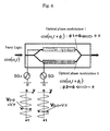
- FIG. 6 is a schematic diagram showing an optical phase modulator for DPSK.
- the DPSK modulation stands for "Differential Phase Shift Keying" modulation.
- an input signal 1 (voltages are 0 and V ⁇ ) is input to an input port 1.
- a signal of opposite polarity 2 (voltages are 0 and -V II ) of the input signal 1 is input to an input port 2.
- Optical signals output in both of the states are both in states in which the light intensity is at the maximum.
- respective beams of the emitted light from both of branched waveguides 9A and 9B intensify each other upon the interference, and the light intensity thus takes the maximum value after theinterference.
- the intensity of multiplexed light is represented by an equation 1.
- the phase difference between both the states is ⁇ radian, and the DPSK modulation is thus enabled.
- an input signal 1 (voltages are 0 and V II ) is input to the input port 1.
- a signal of opposite polarity 2 (voltages are 0 and -V II ) of the input signal 1 is input to an input port 2.
- Optical signals output in both of the states are both in states in which the light intensity is at the maximum.
- respective beams of the emitted light from both of branched waveguides 9A and 9B intensify each other upon the interference; the light intensity thus takes the maximum value after the interference.
- the phase difference is ⁇ radian, and the DPSK modulation is thus enabled.
- phase modulators in FIGS. 3 and 5 can be used for DQPSK (Differential Quadrature Phase Shift Keying) and SSB (Single Side Band amplitude modulation) in addition to DPSK.
- DQPSK Different Quadrature Phase Shift Keying
- SSB Single Side Band amplitude modulation
- the widths of the upper and lower ground electrodes (W GND2 and W GND3 ) and the width of the common ground electrode (W GND ) are preferably equal to each other (refer to FIG. 4 ).
- FIG. 7 is a plan view schematically showing an optical phase modulator 21B according to yet another embodiment. The cross section thereof is similar to that shown in FIG. 4 .
- the optical modulator 21B is provided with the substrate 10 in a planar shape, for example.
- the signal electrodes 3A and 3B, the common ground electrode 22, the first ground electrode 2A and second ground electrode 4A are formed on the surface 10a of the substrate 10.
- the optical waveguides 9A and 9B are formed in the first gaps 7A and 7B, respectively.
- An optical waveguide is not formed in the second gaps 8A and 8B.
- the sizes (widths) of the second gaps 8A and 8B are larger than the sizes (widths) of the first gaps 7A and 7B, respectively.
- Respective beams of light propagating through the optical waveguides 9A and 9B are modulated by phase modulation by applying signal voltages between the signal electrodes 3A and 3B and the respective ground electrodes, thereby forming optical phase modulation portions C and D, respectively.
- Reference numeral 5 denotes the power supply lines to the signal electrodes
- reference numeral 13 denotes the power supply line to the common ground electrode.
- a ratio W/G 1 of the width W of the signal electrode to the size G 1 of the first gap is equal to or more than 2.3.
- W/G 1 is more preferably equal to or more than 4.0.
- W/G 1 is preferable in terms of reduction of the electrode loss.
- W/G 1 is preferably equal to or less than 15.
- G 2 is preferably equal to or less than 1 mm, more preferably equal to or less than 500 microns, and still more preferably equal to or less than 150 microns.
- the optical phase modulator 1 as shown in FIGS. 1 and 2 was produced, and a phase modulation experiment was carried out. Sizes are set as follows (refer to FIG. 2 ).
- an X-cut lithium niobate substrate was used as the electric-optical substrate 10.
- the effective refractive index of microwave was 2.2, and the microwave and light are velocity-matched.
- the characteristic impedance was 43 ⁇ .
- the half-wave voltage V II decreased down to 3.3V when the interaction length of the electrodes was 32 mm.
- the optical phase modulator 21 as shown in FIGS. 3 and 4 was produced, and a phase modulation experiment was carried out. It should be noted that the following dimensions were set.
- the electric-optical substrate 1 an X-cut lithium niobate substrate was used. With this structure, the effective refractive index of microwave was 2.2, and the microwave and light are velocity-matched. The following data were obtained under these conditions.
- the LN substrate thickness Tsub was set to 7 ⁇ m, and the electrode gaps G 2 was variously changed.
- the electrode gaps G 2 were 40, 60, 90 and 150 ⁇ m
- the characteristic impedance Z were changed to 36, 39, 41 and 42 ⁇ , respectively.
- the characteristic impedance significantly increases by increasing the electrode gap G 2 .
- the LN substrate thickness Tsub was set to 4.5 ⁇ m, and the electrode gaps G 2 were variously changed.
- the characteristic impedance Z were changed to 45, 49, 51 and 52 ⁇ , respectively.
- the characteristic impedance significantly increases by increasing the electrode gap G 2 .
- the optical phase modulator 1 as shown in FIGS. 1 and 2 was produced, and a phase modulation experiment was carried out. Sizes are set as follows (refer to FIG. 2 ).
- the electrode loss can be especially reduced.
Landscapes
- Physics & Mathematics (AREA)
- Nonlinear Science (AREA)
- Electromagnetism (AREA)
- Chemical & Material Sciences (AREA)
- Engineering & Computer Science (AREA)
- Ceramic Engineering (AREA)
- Crystallography & Structural Chemistry (AREA)
- General Physics & Mathematics (AREA)
- Optics & Photonics (AREA)
- Optical Modulation, Optical Deflection, Nonlinear Optics, Optical Demodulation, Optical Logic Elements (AREA)
Abstract
Description
- The present invention relates to an optical phase modulator.
- "Band Operation of Guided-Wave Light Modulators with Filter-Type Coplanar Electrodes", IEICE TRANS. ELECTRON., VOL. E78-C, No. 1, January 1995 discloses a optical phase modulator using so-called ACPS electrodes. In this modulator, a channel optical waveguide is formed between a ground electrode and a signal electrode of the ACPS electrodes, and a voltage is impressed on the optical waveguide, thereby modulating the phase of propagating light.
- On the other hand, Japanese Patent Publication No.
H2-269309A - Japanese Patent Publication No.
2005-91698A - Japanese Patent Publication No.
2004-219600A - The present inventor had tried to produce an optical phase modulator which is high in operation stability, and a drive voltage of which is low after impedance matching has been carried out. For example, in the optical phase modulator according to "Band Operation of Guided-Wave Light Modulators with Filter-Type Coplanar Electrodes", IEICE TRANS. ELECTRON., VOL. E78-C, No. 1, January 1995, it is difficult to decrease the drive voltage after the characteristic impedance of the electrodes has been matched to the coaxial line. Further, since it does not have a structure as coplanar electrodes in which a signal electrode is arranged between ground electrodes, it has a defect that electric field confinement is weak, due to an discontinuous points in a bent portion of the signal electrode, a connection portion to a radio frequency coaxial cable, and the like, a radio frequency characteristic tends to show ripples.
- In the respective modulators according to Japanese Patent Publication Nos.
H2-269309A 2005-91698A - It is therefore an object of the present invention to provide an optical phase modulator which has high operation stability, and has a low drive voltage after the impedance has been matched.
- An optical phase modulator of the present invention comprises:
- a substrate comprising an electro-optical material;
- a signal electrode provided on the substrate;
- first and second ground electrodes provided on opposite sides of the signal electrode; and
- an optical phase modulation portion comprising an optical waveguide provided in a first gap between the first ground electrode and the signal electrode, wherein:
- a size G1 of the first gap between the first ground electrode and the signal electrode is smaller than a size G2 of a second gap between the second ground electrode and the signal electrode;
- an optical waveguide is not provided in the second gap; and
- a modulation voltage is applied on the first ground electrode and the signal electrode to modulate the phase of light propagating through the optical waveguide.
- According to the present invention, the size G1 of the first gap between the first ground electrode and the signal electrode is smaller than the size G2 of the second gap between the second ground electrode and the signal electrode, and then, an optical waveguide is not provided in the second gap. Then, the phase of light propagating through the optical waveguide provided in the first gap is modulated by applying a modulation voltage on the first ground electrode and the signal electrode.
- In this way, by providing the optical waveguide in the first gap, the operation stability can be increased. Then, the first gap width is made smaller than the second gap width, and the optical waveguide is provided in the narrower first gap and is not provided in the wider second gap. Since the first gap is narrower in width, the electric field intensity applied to the optical waveguide in the gap is large, and the drive voltage required for predetermined phase modulation decreases compared with a case of an ordinary symmetrical CPW electrodes. On the other hand, though the electric field intensity applied to the optical waveguide in the wider second gap becomes small, since the optical phase modulation is carried out, an optical waveguide is not formed in the second gap. Then, by providing the second gap wider in width, the characteristic impedance of the electrodes can be increased thereby promoting the impedance matching. Further, by providing the signal electrode between the two ground electrodes, the electric field confinement can be increased, thereby realizing excellent radio frequency characteristics without ripples.
- In the optical phase modulator described in "Band Operation of Guided-Wave Light Modulators with Filter-Type Coplanar Electrodes", IEICE TRANS. ELECTRON., VOL. E78-C, No. 1, January 1995, if the gap is increased for characteristic impedance matching, the drive voltage required for the phase modulation increases.
- Since the respective chirp optical amplitude modulators according to Japanese Patent Publication Nos.
H2-269309A 2005-91698A -
-
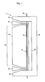
FIG. 1 is a plan view schematically showing anoptical phase modulator 1 according to an embodiment of the present invention; -
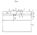
FIG. 2 is a cross sectional view of the optical phase modulator shown inFIG. 1 ; -
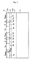
FIG. 3 is a plan view of anoptical phase modulator 21 according to another embodiment of the present invention; -
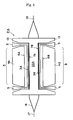
FIG. 4 is a cross sectional view of the optical phase modulators shown inFIGS. 3 ,5 and7 ; -
FIG. 5 is a plan view of anoptical phase modulator 21A according to a still another embodiment of the present invention; -
FIG. 6 is a schematic diagram describing the DPSK optical modulation; and -
FIG. 7 is a plan view of anoptical phase modulator 21B according to yet another embodiment of the present invention. - A more detailed description will now be given of the present invention properly referring to drawings.
-
FIG. 1 is a plan view schematically showing anoptical modulator 1 according to the present invention, andFIG. 2 is a cross sectional view thereof (hatching is omitted). Theoptical modulator 1 is provided with asubstrate 10 in a planar shape, for example. Asignal electrode 3, afirst ground electrode 2, and asecond ground electrode 4 are formed on asurface 10a of thesubstrate 10. An optical waveguide 9 is formed in afirst gap 7, and an optical waveguide is not formed in asecond gap 8. A size (width) of thesecond gap 8 is larger than a size (width) of thefirst gap 7. Light propagating through the optical waveguide 9 is modulated by phase modulation by applying a signal voltage between thesignal electrode 3 and thefirst ground electrode 2, thereby forming an optical phase modulation portionA. Reference numeral 5 denotes a power supply line to the signal electrode, andreference numeral 6 denotes a power supply line to the second ground electrode. - In the
electrode gap 7 relatively narrower in width, since the electric field intensity applied to the optical waveguide is higher, though the drive voltage can be reduced, the characteristic impedance of the electrodes tends to decrease. On the other hand, theelectrode gap 8 relatively wider in width does not modulate the light by the phase modulation, and tends to increase the characteristic impedance of the electrodes. - In the example shown in
FIG. 2 , theoptical waveguide substrate 10 is joined to asupport base 12 via a joining layer 11. As a result, even if thesubstrate 10 is thinned to 100 µm or less, for example, it is possible to prevent thesubstrate 10 from generating a crack while being handled. - According to the present invention, a material for constructing the substrate on which the optical waveguide and the electrodes are formed is a ferroelectric electro-optical material, preferably a single crystal. The crystal is not specifically limited as long as it can modulate light, and, lithium niobate, lithium tantalite, lithium niobate-lithium tantalite solid solution, potassium lithium niobate, KTP, GaAs and rock crystal can be examples thereof.
- A material for the ground electrodes and the signal electrode is not specifically limited as long as it presents a low resistance, and is excellent in impedance characteristic, and the ground electrodes and the signal electrode can be constructed by any material such as gold, silver and copper.
- According to a preferred embodiment, a buffer layer is not provided between the optical waveguide substrate and the electrodes. As a result, it is possible to further reduce the drive voltage required for the phase modulation of the light propagating through the optical waveguide. Especially, when G1 is reduced extremely, if a buffer layer is present on the surface (under the electrodes) of the optical waveguide substrate, the distance between the modulation electrodes and the optical waveguide increases, the modulation electric field in the crosswise direction becomes very weak, and, as a result, even if G1 is reduced, the drive voltage will not decrease, or, conversely, will increase. If there is no buffer layer, even if G1 is reduced, the modulation electric field in the crosswise direction is efficiently impressed on the optical waveguide, and a lower drive voltage is realized for a narrower gap G1.
- The optical waveguide is formed in or on the substrate, and is preferably formed on the surface side of the substrate. The optical waveguide may be a ridge-type optical waveguide directly formed on the surface of the substrate, a ridge-type optical waveguide formed, via another layer, on the surface of the substrate, and an optical waveguide formed inside the substrate by an internal diffusion method or an ion exchange method such as titanium diffused optical waveguide, and a proton exchange optical waveguide. Though the electrodes are provided on the substrate surface side, the electrodes may be formed directly on the substrate surface, and may be formed on a buffer layer.
- Though the type of an adhesive for adhering the substrate and the support base to each other is not specifically limited, the thickness thereof is preferably equal to or less than 300 µm. Moreover, for a low dielectric constant material used as the low dielectric constant layer, in terms of reduction of the propagation loss of a radio frequency modulated signal, a material having a low dielectric loss (low tanδ) is preferably employed. As the material with a low dielectric constant and a low dielectric loss as described above, Teflon and acryl adhesives can be exemplified. Moreover, as other low dielectric constant material, a glass adhesive, an epoxy adhesive, an inter-layer insulating material for semiconductor production, and a polyimide resin can be exemplified.
- The optical phase modulator according to the present invention implies an optical phase modulator which applies phase modulation to incident light, and extracts a phase-modulated signal from emitted light. Thus, as long as the optical phase modulator is intended for the phase modulation, the type thereof is not limited, and various phase modulation such as DQPSK and SSB can be used. In an optical amplitude modulator using a Mach-Zehnder optical waveguide, though the phase of light is modulated in respective branched waveguides, beams of emitted light of the respective branched waveguides are multiplexed, thereby determining whether value is 0 (zero) or 1 (one) according to the amplitude of the multiplexed light. This corresponds to modulation of the amplitude of the emitted light (multiplexed light), and thus, does not correspond to the optical phase modulator according to the present invention.
- According to the present invention, the size G1 of the first gap between the first ground electrode and the signal electrode is smaller than the size G2 of the second gap between the second ground electrode and the signal electrode. On this occasion, the ratio of G2 to G1 (G2/G1) is preferably equal to or more than 1.3, more preferably equal to or more than 2.0, and most preferably equal to or more than 3.0. Moreover, G1 is preferably 2 to 30 µm, and more preferably 8 to 18 µm. Moreover, G2 is preferably 3 to 200 µm, and more preferably 20 to 130 µm.
- According to a preferred embodiment, the thickness of the substrate is equal to or less than 100 µm, and the substrate includes the support base, and the attachment layer that attaches the support base and the substrate to each other. This embodiment is shown in
FIG. 2 . - Moreover, according to a preferred embodiment, the optical phase modulator includes multiple optical phase modulation portions. In this embodiment, the first ground electrode or the second ground electrode of one of the optical phase modulation portions preferably forms a common ground electrode along with the first ground electrode or the second ground electrode of a neighboring one of the optical phase modulation portions. It is possible to reduce the size necessary for the optical phase modulation portions by forming the common ground electrode in this form, thereby contributing to the downsizing of the chip.
- In this embodiment, the width of the common ground electrode is preferably wider than the width of the respective signal electrodes of the respective optical phase modulators, thereby preventing influence from the neighboring optical phase modulation portion. Moreover, though there is no upper limit for the width of the common ground electrode, in terms of the downsizing of the optical phase modulator chip, the width is preferably 300 µm or less, more preferably 200 µm or less, and still more preferably 150 µm or less.
- Moreover, according to a preferred embodiment, the width of the common ground electrode is equal to the respective widths of the respective ground electrodes other than the common ground electrode. It should be noted that a manufacturing error is permitted on this occasion.
- According to a preferred embodiment, the phases of the respective beams of light propagating through the multiple optical waveguides are modulated, the respective beams of modulated light are multiplexed, and information on the phase modulation is obtained from the multiplexed light.
-
FIG. 3 is a plan view schematically showing anoptical modulator 21 according to another embodiment, andFIG. 4 is a cross sectional view thereof (hatching is omitted). Theoptical modulator 21 is provided with thesubstrate 10 in a planar shape, for example.Signal electrodes common ground electrode 22, afirst ground electrode 2A, and asecond ground electrode 4A are formed on thesurface 10a of thesubstrate 10.Optical waveguides first gaps second gaps second gaps first gaps optical waveguides signal electrodes first ground electrodes Reference numeral 5 denotes power supply lines to the signal electrodes, andreference numeral 13 denotes a power supply line to the common ground electrode. - In the
electrode gaps electrode gaps - In the example shown in
FIG. 4 , theoptical waveguide substrate 10 is joined to thesupport base 12 via the joining layer 11. As a result, even if thesubstrate 10 is thinned, it is possible to prevent thesubstrate 10 from generating a crack while being handled. -
FIG. 5 is a plan view schematically showing anoptical modulator 21A according to a still another embodiment. The cross section thereof is similar to that shown inFIG. 4 . Theoptical modulator 21A is provided with thesubstrate 10 in a planar shape, for example. Thesignal electrodes common ground electrode 22A, andsecond ground electrodes surface 10a of thesubstrate 10. Theoptical waveguides first gaps second gaps second gaps first gaps optical waveguides signal electrodes common ground electrode 22A, thereby forming the optical phase modulation portions A and B, respectively.Reference numeral 5 denotes the power supply lines to the signal electrodes, andreference numeral 13 denotes the power supply line to the common ground electrode. - According to the present embodiment, the optical waveguides form a Mach-Zehnder optical waveguide. In other words, light made incident from an
incident portion 17 is branched in abranch portion 18, and branched beams of light are made incident to the respectiveoptical waveguides portion 19, and multiplexed light is output from the modulator. Information on a phase-modulated signal is obtained from the output modulated light. - The type of the phase modulation for the case in which the multiple optical phase modulation portions are used is not limited, and various phase modulation types such as DQPSK, SSB and DPSK may be employed. The respective types of the modulation themselves are known.
- For example,
FIG. 6 is a schematic diagram showing an optical phase modulator for DPSK. The DPSK modulation stands for "Differential Phase Shift Keying" modulation. First, an input signal 1 (voltages are 0 and Vπ) is input to aninput port 1. At the same time, a signal of opposite polarity 2 (voltages are 0 and -VII) of theinput signal 1 is input to aninput port 2. - As a result, the following two states arise:
- State 1: 0 V on the
input port 1, and 0 V on theinput port 2, and - State 2: VII V on the
input port 1, and -VII V on theinput port 2. - Optical signals output in both of the states are both in states in which the light intensity is at the maximum. In other words, respective beams of the emitted light from both of
branched waveguides equation 1. Then, the phase difference between both the states is π radian, and the DPSK modulation is thus enabled.
- On the other hand, a description will be given of a case in which the same signal (voltage: VII) is impressed on the two radio frequency input ports with reference to the modulator in
FIG. 5 as an example. Due to the difference in the electrode arrangement, the direction of the line of electric force applied to the optical waveguides is different from those of the case shown inFIG. 3 . - First, an input signal 1 (voltages are 0 and VII) is input to the
input port 1. At the same time, a signal of opposite polarity 2 (voltages are 0 and -VII) of theinput signal 1 is input to aninput port 2. - As a result, the following two states arise:
- State 1: 0V on the
input port 1, and 0V on theinput port 2, and - State 2: VII V on the
input port 1, and VII V on theinput port 2. - Optical signals output in both of the states are both in states in which the light intensity is at the maximum. In other words, respective beams of the emitted light from both of
branched waveguides - Obviously, the respective phase modulators in
FIGS. 3 and5 can be used for DQPSK (Differential Quadrature Phase Shift Keying) and SSB (Single Side Band amplitude modulation) in addition to DPSK. - When the common ground electrode is used, in terms of coinciding the drive voltages (half-wave voltages) for the two optical phase modulation portions, as describe before, the widths of the upper and lower ground electrodes (WGND2 and WGND3) and the width of the common ground electrode (WGND) are preferably equal to each other (refer to
FIG. 4 ). - Moreover, the phases of the respective beams of light propagating through multiple optical waveguides can be independently modulated.
FIG. 7 is a plan view schematically showing anoptical phase modulator 21B according to yet another embodiment. The cross section thereof is similar to that shown inFIG. 4 . Theoptical modulator 21B is provided with thesubstrate 10 in a planar shape, for example. Thesignal electrodes common ground electrode 22, thefirst ground electrode 2A andsecond ground electrode 4A are formed on thesurface 10a of thesubstrate 10. Theoptical waveguides first gaps second gaps second gaps first gaps optical waveguides signal electrodes Reference numeral 5 denotes the power supply lines to the signal electrodes, andreference numeral 13 denotes the power supply line to the common ground electrode. - Then, modulated light modulated by the optical phase modulation portion C is emitted from the
optical waveguide 9A, and the phase modulation signal is detected from the emitted light. Moreover, modulated light modulated by the optical phase modulation portion D is emitted from theoptical waveguide 9B, and the phase modulation signal is detected from the emitted light. - According to a preferred embodiment, a ratio W/G1 of the width W of the signal electrode to the size G1 of the first gap is equal to or more than 2.3. As a result, the electrode loss decreases significantly. In this respect, W/G1 is more preferably equal to or more than 4.0.
- A larger W/G1 is preferable in terms of reduction of the electrode loss. However, if W/G1 excessively increases, the device becomes large, the characteristic impedance decreases, and the perfect velocity matching between the lightwave and the microwave becomes difficult. Therefore, W/G1 is preferably equal to or less than 15.
- If G2 is excessively large, due to the asymmetry of the electrodes, ripples in terms of the radio frequency characteristics increases. Therefore, G2 is preferably equal to or less than 1 mm, more preferably equal to or less than 500 microns, and still more preferably equal to or less than 150 microns.
- The
optical phase modulator 1 as shown inFIGS. 1 and2 was produced, and a phase modulation experiment was carried out. Sizes are set as follows (refer toFIG. 2 ). - G1 = 16 µm, G2 = 92 µm, W = 38 µm, Tm = 20 µm,
- Tsub = 7.0 µm, Tad = 50 µm, and relative permittivity of the low dielectric constant layer 11: 4.0.
- As the electric-
optical substrate 10, an X-cut lithium niobate substrate was used. With this structure, the effective refractive index of microwave was 2.2, and the microwave and light are velocity-matched. The characteristic impedance was 43 Ω. Moreover, the half-wave voltage VII decreased down to 3.3V when the interaction length of the electrodes was 32 mm. - The
optical phase modulator 21 as shown inFIGS. 3 and4 was produced, and a phase modulation experiment was carried out. It should be noted that the following dimensions were set. - W = 40 µm, G1 = 16.5 µm, G2 = 90 µm,
- WGND = WGND2 = WGND3 = 100 µm, Tsub = 7 µm,
- electrode thickness Tm = 17 µm, and electrode interaction length L = 3.2 cm.
- As the electric-
optical substrate 1, an X-cut lithium niobate substrate was used. With this structure, the effective refractive index of microwave was 2.2, and the microwave and light are velocity-matched. The following data were obtained under these conditions. - Electrode conductor loss α = 0.33 dB•cm-1•GHz-1/2
- Characteristic impedance Z = 41 Ω
- Half wave voltage Vπ = 3.4 V
- Product of half wave voltage and interaction length VπL = 10.8 V•cm
- 3 dB band width ΔF3 dB = 25 GHz
- Dependency on the ground electrode width WGND was investigated in the second example. In other words, in
FIG. 4 , only WGND was variously changed. As a result, when the ground electrode widths WGND were 50, 150, 200 and 500 µm, the electrode propagation loss α were respectively 0.34, 0.32 and 0.31 dB•cm-1•GHz-1/2. Even when WGND is decreased down to approximately 50 µm, it is appreciated that the electrode propagation loss does not change so much. - Dependency on the electrode gap G1 was investigated in the second example. In other words, in
FIG. 4 , only the electrode gap G1 was variously changed. As a result, when the electrode gaps G1 were 20, 13.5 and 10 µm, the drive voltage VπL were respectively 12.7, 9.2 and 7.5 V•cm. In this way, the drive voltage is significantly reduced by reducing the gap G1. - Dependency on the electrode gap G2 was investigated in the second example. In other words, in
FIG. 4 , the LN substrate thickness Tsub was set to 7 µm, and the electrode gaps G2 was variously changed. As a result, when the electrode gaps G2 were 40, 60, 90 and 150 µm, the characteristic impedance Z were changed to 36, 39, 41 and 42 Ω, respectively. In other words, the characteristic impedance significantly increases by increasing the electrode gap G2. - Dependency on the ground electrode gap G2 was investigated in the second example. In other words, in
FIG. 4 , the LN substrate thickness Tsub was set to 4.5 µm, and the electrode gaps G2 were variously changed. As a result, when the electrode gaps G2 were 40, 60, 90 and 150 µm, the characteristic impedance Z were changed to 45, 49, 51 and 52 Ω, respectively. In other words, the characteristic impedance significantly increases by increasing the electrode gap G2. - Dependency on the center conductor width W was investigated in the second example. In other words, when W were changed to 20, 60 and 100 µm, the electrode propagation loss α were respectively 0.36, 0.30 and 0.28 dB•cm-1•GHz-1/2.
- The
optical phase modulator 1 as shown inFIGS. 1 and2 was produced, and a phase modulation experiment was carried out. Sizes are set as follows (refer toFIG. 2 ). - G1 = 13.5 µm, G2 = 70 µm, Tsub = 5.0 µm, Tad = 100 µm, and
- relative permittivity of the low dielectric constant layer 11: 4.0.
- As the electric-
optical substrate 10, an X-cut lithium niobate substrate was used. For this structure, detailed simulation was carried out using the FEM, and respective dimensional conditions which attain a state in which the microwave effective index is 2.2, and the characteristic impedance is approximately 45 Ω were searched for. It should be noted that the signal electrode width W and the electrode thickness Tm were changed. As a result, respective dimensional conditions shown in a Table 1 were obtained. Then, for the respective dimensional conditions shown in Table 1, the electrode propagation loss α was calculated, and shown in the Table 1.Table 1 W/G1 W Tm α 1 13.5 13 0.327 1.5 20.25 11.5 0.303 2 27 10.3 0.284 2.3 31.05 9.5 0.275 2.5 33.75 9.2 0.27 3 40.5 8.3 0.258 3.5 47.25 7.5 0.247 4 54 6.8 0.237 4.5 60.75 6.1 0.229 5 67.5 5.6 0.222 5.5 74.25 5 0.216 6 81 4.4 0.21 6.5 87.75 4 0.205 7 94.5 3.5 0.2 7.5 101.25 3 0.195 8 108 2.5 0.192 8.5 114.75 2.3 0.188 9 121.5 1.8 0.184 9.5 128.25 1.4 0.181 10 135 1.1 0.178 - The
optical phase modulator 1 as shown inFIGS. 1 and2 was produced, and a phase modulation experiment was carried out. Sizes are set as follows (refer toFIG. 2 ). - G1 = 16.5 µm, G2 = 90 µm, Tsub = 7.0 µm, Tad = 50 µm, and
- relative permittivity of the low dielectric constant layer 11: 4.0.
- As the electric-
optical substrate 10, an X-cut lithium niobate substrate was used. For this structure, detailed simulation was carried out using the FEM, and respective dimensional conditions which attain a state in which the microwave effective index is 2.2, and the characteristic impedance is approximately 45 Ω were searched for. It should be noted that the signal electrode width W and the electrode thickness Tm were changed. As a result, respective dimensional conditions shown in Table 2 were obtained. Then, for the respective dimensional conditions shown in Table 2, the electrode propagation loss α was calculated, and shown in the Table 2.Table 2 W/G W Tm α 1 16.5 20.0 0.265 1.5 24.75 18.3 0.246 2 33 16.9 0.232 2.3 37.95 16.2 0.225 2.5 41.25 15.7 0.221 3 49.5 14.6 0.212 3.5 57.75 13.7 0.204 4 66 13.0 0.197 4.5 74.25 12.0 0.191 5 82.5 11.2 0.185 5.5 90.75 10.5 0.18 6 99 9.8 0.176 6.5 107.25 9.2 0.171 7 115.5 8.6 0.167 7.5 123.75 8.1 0.164 8 132 7.6 0.16 8.5 140.25 7.1 0.157 9 148.5 6.6 0.154 9.5 156.75 6.2 0.152 10 165 5.7 0.149 11 181.5 4.7 0.145 12 198 3.8 0.141 13 214.5 3.0 0.138 14 231 2.4 0.135 15 247.5 1.6 0.133 - As shown in the Tables 1 and 2, when W/G1 is equal to or more than 2.3, and equal to or less than 15, and G2 is equal to or more than 2G1, and equal to or less than 1 mm, the electrode loss can be especially reduced.
Claims (9)
- An optical phase modulator comprising:a substrate comprising an electro-optical material;a signal electrode provided on the substrate;first and second ground electrodes provided on both sides of the signal electrode; andan optical phase modulation portion comprising an optical waveguide provided in a first gap between the first ground electrode and the signal electrode, wherein:a size G1 of the first gap between the first ground electrode and the signal electrode is smaller than a size G2 of a second gap between the second ground electrode and the signal electrode;an optical waveguide is not provided in the second gap; anda modulation voltage is applied on the first ground electrode and the signal electrode to modulate the phase of light propagating through the optical waveguide.
- The optical phase modulator of claim 1, further comprising a support base and a bonding layer bonding the support base and the substrate, wherein the substrate has a thickness equal to or less than 100 µm.
- The optical phase modulator of claim 1 or 2, comprising a plurality of the optical phase modulation portions.
- The optical phase modulator of claim 3, wherein either one of the first ground electrode and the second ground electrode of one of the plurality of optical phase modulation portions forms a common ground electrode along with either one of the first ground electrode and the second ground electrode of a neighboring one of the optical phase modulation portions.
- The optical phase modulator of claim 4, wherein the common ground electrode has a width equal to or more than the width of the signal electrode and equal to or less than 300 µm.
- The optical phase modulator of any one of claims 3 to 5, wherein the phases of the respective beams of light propagating through a plurality of the optical waveguides are independently modulated.
- The optical phase modulator of any one of claims 3 to 5, wherein the phases of the respective beams of light propagating through the plurality of optical waveguides are modulated, the respective beams of modulated light are multiplexed, and information on the phase modulation is obtained from the multiplexed light.
- The optical phase modulator of any one of claims 1 to 7, wherein a ratio W/G1 of a width W of the signal electrode to the size G1 of the first gap is equal to or more than 2.3.
- The optical phase modulator of any one of claims 1 to 8, wherein a ratio G2/G1 of the size G2 of the second gap to the size G1 of the first gap is equal to or more than 2.0.
Applications Claiming Priority (2)
| Application Number | Priority Date | Filing Date | Title |
|---|---|---|---|
| JP2007055261 | 2007-03-06 | ||
| PCT/JP2008/052605 WO2008108154A1 (en) | 2007-03-06 | 2008-02-12 | Optical phase modulator |
Publications (3)
| Publication Number | Publication Date |
|---|---|
| EP2116889A1 true EP2116889A1 (en) | 2009-11-11 |
| EP2116889A4 EP2116889A4 (en) | 2011-10-05 |
| EP2116889B1 EP2116889B1 (en) | 2014-08-06 |
Family
ID=39738051
Family Applications (1)
| Application Number | Title | Priority Date | Filing Date |
|---|---|---|---|
| EP08711429.4A Active EP2116889B1 (en) | 2007-03-06 | 2008-02-12 | Optical phase modulator |
Country Status (4)
| Country | Link |
|---|---|
| US (1) | US7869669B2 (en) |
| EP (1) | EP2116889B1 (en) |
| JP (1) | JP5171808B2 (en) |
| WO (1) | WO2008108154A1 (en) |
Cited By (1)
| Publication number | Priority date | Publication date | Assignee | Title |
|---|---|---|---|---|
| EP2876495A1 (en) * | 2013-11-25 | 2015-05-27 | Fraunhofer-Gesellschaft zur Förderung der angewandten Forschung e.V. | Electrical line arrangement |
Families Citing this family (16)
| Publication number | Priority date | Publication date | Assignee | Title |
|---|---|---|---|---|
| GB2493690B (en) * | 2011-05-20 | 2018-01-17 | Univ Surrey | Optical communication system |
| EP2843462A4 (en) * | 2012-04-27 | 2015-12-30 | Nec Corp | Mach-zehnder type optical modulator, optical transmitting/receiving system, and mach-zehnder type optical modulator control method |
| JP5812142B2 (en) | 2014-03-28 | 2015-11-11 | 住友大阪セメント株式会社 | Optical waveguide device module |
| JP6107868B2 (en) * | 2015-03-31 | 2017-04-05 | 住友大阪セメント株式会社 | Optical waveguide device |
| JP2018036398A (en) * | 2016-08-30 | 2018-03-08 | 株式会社フジクラ | Substrate type optical waveguide and substrate type optical modulator |
| JP2018036399A (en) | 2016-08-30 | 2018-03-08 | 株式会社フジクラ | Substrate type optical waveguide and substrate type optical modulator |
| CN107957629A (en) * | 2016-10-18 | 2018-04-24 | 天津领芯科技发展有限公司 | Wideband lithium niobate electrooptic modulator based on teflon material cushion |
| CN108020939A (en) * | 2016-10-31 | 2018-05-11 | 天津领芯科技发展有限公司 | A kind of LiNbO_3 film QPSK optical modulators and its manufacture method |
| JP6853213B2 (en) * | 2018-04-19 | 2021-03-31 | 日本電信電話株式会社 | Mach Zenda Modulator |
| US12282214B2 (en) | 2019-11-27 | 2025-04-22 | HyperLight Corporation | Thin film lithium niobate optical device having an engineered substrate for heterogeneous integration |
| US12656637B1 (en) | 2019-11-27 | 2026-06-16 | HyperLight Corporation | Lithium niobate photonic devices having engineered lithium niobate, silicon dioxide, and electrode extension thickness |
| US12601938B2 (en) | 2019-11-27 | 2026-04-14 | HyperLight Corporation | Electro-optic devices having closely spaced engineered electrodes |
| JP7701354B2 (en) * | 2019-11-27 | 2025-07-01 | ハイパーライト・コーポレーション | Electro-optical device having improved electrodes |
| CN115885208A (en) | 2020-06-02 | 2023-03-31 | 超光公司 | High Performance Optical Modulators and Drivers |
| US12416824B1 (en) * | 2022-02-03 | 2025-09-16 | National Technology & Engineering Solutions Of Sandia, Llc. | Ultraviolet and visible light integrated acousto-optic modulators |
| CN116699881A (en) * | 2022-02-25 | 2023-09-05 | 苏州极刻光核科技有限公司 | Electro-optic modulator |
Family Cites Families (13)
| Publication number | Priority date | Publication date | Assignee | Title |
|---|---|---|---|---|
| JP2679223B2 (en) | 1989-03-14 | 1997-11-19 | 富士通株式会社 | Optical modulation method and optical modulator |
| CA2011954C (en) | 1989-03-14 | 1994-02-22 | Fujitsu Limited | Optical modulator |
| US5050948A (en) * | 1990-08-23 | 1991-09-24 | Tektronix, Inc. | Traveling wave electro-optic modulator |
| JPH09211403A (en) * | 1996-02-01 | 1997-08-15 | Nippon Telegr & Teleph Corp <Ntt> | Light control element |
| JP3067760B1 (en) * | 1999-03-02 | 2000-07-24 | 住友大阪セメント株式会社 | Waveguide type optical device |
| US6449080B1 (en) | 2000-03-08 | 2002-09-10 | Jds Uniphase Corporation | Electro-optic modulator with enhanced bias stability |
| JP3362126B2 (en) | 2000-03-09 | 2003-01-07 | 住友大阪セメント株式会社 | Optical waveguide device |
| JP2004219600A (en) * | 2003-01-14 | 2004-08-05 | Ngk Insulators Ltd | Electrode for optical modulation and optical modulator |
| JP2005091698A (en) * | 2003-09-17 | 2005-04-07 | Ngk Insulators Ltd | Optical modulator |
| US7324257B2 (en) * | 2004-07-27 | 2008-01-29 | Jds Uniphase Corporation | Low bias drift modulator with buffer layer |
| JP2007133135A (en) * | 2005-11-10 | 2007-05-31 | Ngk Insulators Ltd | Optical waveguide device |
| JP2007139958A (en) * | 2005-11-16 | 2007-06-07 | Ngk Insulators Ltd | Optical waveguide device |
| JP2009145816A (en) * | 2007-12-18 | 2009-07-02 | Ngk Insulators Ltd | Optical modulator |
-
2008
- 2008-02-12 EP EP08711429.4A patent/EP2116889B1/en active Active
- 2008-02-12 JP JP2009502499A patent/JP5171808B2/en active Active
- 2008-02-12 WO PCT/JP2008/052605 patent/WO2008108154A1/en not_active Ceased
-
2009
- 2009-07-28 US US12/510,535 patent/US7869669B2/en active Active
Cited By (3)
| Publication number | Priority date | Publication date | Assignee | Title |
|---|---|---|---|---|
| EP2876495A1 (en) * | 2013-11-25 | 2015-05-27 | Fraunhofer-Gesellschaft zur Förderung der angewandten Forschung e.V. | Electrical line arrangement |
| WO2015075259A1 (en) * | 2013-11-25 | 2015-05-28 | Fraunhofer-Gesellschaft zur Förderung der angewandten Forschung e.V. | Electrical line arrangement |
| US10216014B2 (en) | 2013-11-25 | 2019-02-26 | Fraunhofer-Gesellschaft zur Förderung der angewandten Forschung e.V. | Electrical line arrangement |
Also Published As
| Publication number | Publication date |
|---|---|
| US7869669B2 (en) | 2011-01-11 |
| US20090290830A1 (en) | 2009-11-26 |
| JP5171808B2 (en) | 2013-03-27 |
| EP2116889B1 (en) | 2014-08-06 |
| EP2116889A4 (en) | 2011-10-05 |
| JPWO2008108154A1 (en) | 2010-06-10 |
| WO2008108154A1 (en) | 2008-09-12 |
Similar Documents
| Publication | Publication Date | Title |
|---|---|---|
| EP2116889B1 (en) | Optical phase modulator | |
| US7447389B2 (en) | Optical modulator | |
| US7689067B2 (en) | Nested modulator | |
| US10018888B2 (en) | Advanced techniques for improving high-efficiency optical modulators | |
| US7502530B2 (en) | Optical waveguide devices and traveling wave type optical modulators | |
| US6522793B1 (en) | Low voltage electro-optic modulator with integrated driver | |
| US9568751B2 (en) | Optical control device | |
| US7643708B2 (en) | Optical modulator | |
| EP2133733A1 (en) | Light control element | |
| JP2003066394A (en) | Coplanar integrated optical waveguide electro-optic modulator | |
| US20220163827A1 (en) | Optical device, optical communication apparatus, and manufacturing method of the optical device | |
| US20060120654A1 (en) | Optical modulators | |
| JP2009053444A (en) | Optical waveguide element | |
| WO2015151978A1 (en) | Light-control element | |
| US7460739B2 (en) | Lithium niobate optical modulator | |
| JP5229378B2 (en) | Optical waveguide device | |
| US20070081766A1 (en) | Optical waveguide device | |
| US6768570B2 (en) | Optical modulator | |
| JP4587762B2 (en) | Light modulation element module | |
| US11556041B2 (en) | Electro-optic modulator | |
| JP4926423B2 (en) | Light modulator | |
| JP2004219600A (en) | Electrode for optical modulation and optical modulator | |
| JP5622293B2 (en) | Nested modulator | |
| JP2009236996A (en) | Light modulator |
Legal Events
| Date | Code | Title | Description |
|---|---|---|---|
| PUAI | Public reference made under article 153(3) epc to a published international application that has entered the european phase |
Free format text: ORIGINAL CODE: 0009012 |
|
| 17P | Request for examination filed |
Effective date: 20090806 |
|
| AK | Designated contracting states |
Kind code of ref document: A1 Designated state(s): AT BE BG CH CY CZ DE DK EE ES FI FR GB GR HR HU IE IS IT LI LT LU LV MC MT NL NO PL PT RO SE SI SK TR |
|
| DAX | Request for extension of the european patent (deleted) | ||
| A4 | Supplementary search report drawn up and despatched |
Effective date: 20110905 |
|
| RIC1 | Information provided on ipc code assigned before grant |
Ipc: G02F 1/035 20060101AFI20110830BHEP |
|
| GRAP | Despatch of communication of intention to grant a patent |
Free format text: ORIGINAL CODE: EPIDOSNIGR1 |
|
| INTG | Intention to grant announced |
Effective date: 20140224 |
|
| GRAS | Grant fee paid |
Free format text: ORIGINAL CODE: EPIDOSNIGR3 |
|
| GRAA | (expected) grant |
Free format text: ORIGINAL CODE: 0009210 |
|
| AK | Designated contracting states |
Kind code of ref document: B1 Designated state(s): AT BE BG CH CY CZ DE DK EE ES FI FR GB GR HR HU IE IS IT LI LT LU LV MC MT NL NO PL PT RO SE SI SK TR |
|
| REG | Reference to a national code |
Ref country code: GB Ref legal event code: FG4D |
|
| REG | Reference to a national code |
Ref country code: CH Ref legal event code: EP Ref country code: AT Ref legal event code: REF Ref document number: 681291 Country of ref document: AT Kind code of ref document: T Effective date: 20140815 |
|
| REG | Reference to a national code |
Ref country code: IE Ref legal event code: FG4D |
|
| REG | Reference to a national code |
Ref country code: DE Ref legal event code: R096 Ref document number: 602008033688 Country of ref document: DE Effective date: 20140918 |
|
| REG | Reference to a national code |
Ref country code: AT Ref legal event code: MK05 Ref document number: 681291 Country of ref document: AT Kind code of ref document: T Effective date: 20140806 |
|
| REG | Reference to a national code |
Ref country code: NL Ref legal event code: VDEP Effective date: 20140806 |
|
| REG | Reference to a national code |
Ref country code: LT Ref legal event code: MG4D |
|
| PG25 | Lapsed in a contracting state [announced via postgrant information from national office to epo] |
Ref country code: ES Free format text: LAPSE BECAUSE OF FAILURE TO SUBMIT A TRANSLATION OF THE DESCRIPTION OR TO PAY THE FEE WITHIN THE PRESCRIBED TIME-LIMIT Effective date: 20140806 Ref country code: FI Free format text: LAPSE BECAUSE OF FAILURE TO SUBMIT A TRANSLATION OF THE DESCRIPTION OR TO PAY THE FEE WITHIN THE PRESCRIBED TIME-LIMIT Effective date: 20140806 Ref country code: SE Free format text: LAPSE BECAUSE OF FAILURE TO SUBMIT A TRANSLATION OF THE DESCRIPTION OR TO PAY THE FEE WITHIN THE PRESCRIBED TIME-LIMIT Effective date: 20140806 Ref country code: NO Free format text: LAPSE BECAUSE OF FAILURE TO SUBMIT A TRANSLATION OF THE DESCRIPTION OR TO PAY THE FEE WITHIN THE PRESCRIBED TIME-LIMIT Effective date: 20141106 Ref country code: GR Free format text: LAPSE BECAUSE OF FAILURE TO SUBMIT A TRANSLATION OF THE DESCRIPTION OR TO PAY THE FEE WITHIN THE PRESCRIBED TIME-LIMIT Effective date: 20141107 Ref country code: PT Free format text: LAPSE BECAUSE OF FAILURE TO SUBMIT A TRANSLATION OF THE DESCRIPTION OR TO PAY THE FEE WITHIN THE PRESCRIBED TIME-LIMIT Effective date: 20141209 Ref country code: LT Free format text: LAPSE BECAUSE OF FAILURE TO SUBMIT A TRANSLATION OF THE DESCRIPTION OR TO PAY THE FEE WITHIN THE PRESCRIBED TIME-LIMIT Effective date: 20140806 Ref country code: BG Free format text: LAPSE BECAUSE OF FAILURE TO SUBMIT A TRANSLATION OF THE DESCRIPTION OR TO PAY THE FEE WITHIN THE PRESCRIBED TIME-LIMIT Effective date: 20141106 |
|
| PG25 | Lapsed in a contracting state [announced via postgrant information from national office to epo] |
Ref country code: AT Free format text: LAPSE BECAUSE OF FAILURE TO SUBMIT A TRANSLATION OF THE DESCRIPTION OR TO PAY THE FEE WITHIN THE PRESCRIBED TIME-LIMIT Effective date: 20140806 Ref country code: NL Free format text: LAPSE BECAUSE OF FAILURE TO SUBMIT A TRANSLATION OF THE DESCRIPTION OR TO PAY THE FEE WITHIN THE PRESCRIBED TIME-LIMIT Effective date: 20140806 Ref country code: LV Free format text: LAPSE BECAUSE OF FAILURE TO SUBMIT A TRANSLATION OF THE DESCRIPTION OR TO PAY THE FEE WITHIN THE PRESCRIBED TIME-LIMIT Effective date: 20140806 Ref country code: CY Free format text: LAPSE BECAUSE OF FAILURE TO SUBMIT A TRANSLATION OF THE DESCRIPTION OR TO PAY THE FEE WITHIN THE PRESCRIBED TIME-LIMIT Effective date: 20140806 Ref country code: HR Free format text: LAPSE BECAUSE OF FAILURE TO SUBMIT A TRANSLATION OF THE DESCRIPTION OR TO PAY THE FEE WITHIN THE PRESCRIBED TIME-LIMIT Effective date: 20140806 Ref country code: PL Free format text: LAPSE BECAUSE OF FAILURE TO SUBMIT A TRANSLATION OF THE DESCRIPTION OR TO PAY THE FEE WITHIN THE PRESCRIBED TIME-LIMIT Effective date: 20140806 Ref country code: IS Free format text: LAPSE BECAUSE OF FAILURE TO SUBMIT A TRANSLATION OF THE DESCRIPTION OR TO PAY THE FEE WITHIN THE PRESCRIBED TIME-LIMIT Effective date: 20141206 |
|
| PG25 | Lapsed in a contracting state [announced via postgrant information from national office to epo] |
Ref country code: EE Free format text: LAPSE BECAUSE OF FAILURE TO SUBMIT A TRANSLATION OF THE DESCRIPTION OR TO PAY THE FEE WITHIN THE PRESCRIBED TIME-LIMIT Effective date: 20140806 Ref country code: DK Free format text: LAPSE BECAUSE OF FAILURE TO SUBMIT A TRANSLATION OF THE DESCRIPTION OR TO PAY THE FEE WITHIN THE PRESCRIBED TIME-LIMIT Effective date: 20140806 Ref country code: RO Free format text: LAPSE BECAUSE OF FAILURE TO SUBMIT A TRANSLATION OF THE DESCRIPTION OR TO PAY THE FEE WITHIN THE PRESCRIBED TIME-LIMIT Effective date: 20140806 Ref country code: CZ Free format text: LAPSE BECAUSE OF FAILURE TO SUBMIT A TRANSLATION OF THE DESCRIPTION OR TO PAY THE FEE WITHIN THE PRESCRIBED TIME-LIMIT Effective date: 20140806 Ref country code: IT Free format text: LAPSE BECAUSE OF FAILURE TO SUBMIT A TRANSLATION OF THE DESCRIPTION OR TO PAY THE FEE WITHIN THE PRESCRIBED TIME-LIMIT Effective date: 20140806 Ref country code: SK Free format text: LAPSE BECAUSE OF FAILURE TO SUBMIT A TRANSLATION OF THE DESCRIPTION OR TO PAY THE FEE WITHIN THE PRESCRIBED TIME-LIMIT Effective date: 20140806 |
|
| REG | Reference to a national code |
Ref country code: DE Ref legal event code: R097 Ref document number: 602008033688 Country of ref document: DE |
|
| PLBE | No opposition filed within time limit |
Free format text: ORIGINAL CODE: 0009261 |
|
| STAA | Information on the status of an ep patent application or granted ep patent |
Free format text: STATUS: NO OPPOSITION FILED WITHIN TIME LIMIT |
|
| PG25 | Lapsed in a contracting state [announced via postgrant information from national office to epo] |
Ref country code: BE Free format text: LAPSE BECAUSE OF NON-PAYMENT OF DUE FEES Effective date: 20150228 |
|
| 26N | No opposition filed |
Effective date: 20150507 |
|
| PG25 | Lapsed in a contracting state [announced via postgrant information from national office to epo] |
Ref country code: LU Free format text: LAPSE BECAUSE OF FAILURE TO SUBMIT A TRANSLATION OF THE DESCRIPTION OR TO PAY THE FEE WITHIN THE PRESCRIBED TIME-LIMIT Effective date: 20150212 |
|
| REG | Reference to a national code |
Ref country code: CH Ref legal event code: PL |
|
| GBPC | Gb: european patent ceased through non-payment of renewal fee |
Effective date: 20150212 |
|
| PG25 | Lapsed in a contracting state [announced via postgrant information from national office to epo] |
Ref country code: MC Free format text: LAPSE BECAUSE OF FAILURE TO SUBMIT A TRANSLATION OF THE DESCRIPTION OR TO PAY THE FEE WITHIN THE PRESCRIBED TIME-LIMIT Effective date: 20140806 Ref country code: LI Free format text: LAPSE BECAUSE OF NON-PAYMENT OF DUE FEES Effective date: 20150228 Ref country code: CH Free format text: LAPSE BECAUSE OF NON-PAYMENT OF DUE FEES Effective date: 20150228 |
|
| REG | Reference to a national code |
Ref country code: IE Ref legal event code: MM4A |
|
| REG | Reference to a national code |
Ref country code: FR Ref legal event code: ST Effective date: 20151030 |
|
| PG25 | Lapsed in a contracting state [announced via postgrant information from national office to epo] |
Ref country code: SI Free format text: LAPSE BECAUSE OF FAILURE TO SUBMIT A TRANSLATION OF THE DESCRIPTION OR TO PAY THE FEE WITHIN THE PRESCRIBED TIME-LIMIT Effective date: 20140806 |
|
| PG25 | Lapsed in a contracting state [announced via postgrant information from national office to epo] |
Ref country code: GB Free format text: LAPSE BECAUSE OF NON-PAYMENT OF DUE FEES Effective date: 20150212 Ref country code: IE Free format text: LAPSE BECAUSE OF NON-PAYMENT OF DUE FEES Effective date: 20150212 |
|
| PG25 | Lapsed in a contracting state [announced via postgrant information from national office to epo] |
Ref country code: FR Free format text: LAPSE BECAUSE OF NON-PAYMENT OF DUE FEES Effective date: 20150302 |
|
| PG25 | Lapsed in a contracting state [announced via postgrant information from national office to epo] |
Ref country code: BE Free format text: LAPSE BECAUSE OF FAILURE TO SUBMIT A TRANSLATION OF THE DESCRIPTION OR TO PAY THE FEE WITHIN THE PRESCRIBED TIME-LIMIT Effective date: 20140806 |
|
| PG25 | Lapsed in a contracting state [announced via postgrant information from national office to epo] |
Ref country code: MT Free format text: LAPSE BECAUSE OF FAILURE TO SUBMIT A TRANSLATION OF THE DESCRIPTION OR TO PAY THE FEE WITHIN THE PRESCRIBED TIME-LIMIT Effective date: 20140806 |
|
| PG25 | Lapsed in a contracting state [announced via postgrant information from national office to epo] |
Ref country code: HU Free format text: LAPSE BECAUSE OF FAILURE TO SUBMIT A TRANSLATION OF THE DESCRIPTION OR TO PAY THE FEE WITHIN THE PRESCRIBED TIME-LIMIT; INVALID AB INITIO Effective date: 20080212 |
|
| PG25 | Lapsed in a contracting state [announced via postgrant information from national office to epo] |
Ref country code: TR Free format text: LAPSE BECAUSE OF FAILURE TO SUBMIT A TRANSLATION OF THE DESCRIPTION OR TO PAY THE FEE WITHIN THE PRESCRIBED TIME-LIMIT Effective date: 20140806 |
|
| PGFP | Annual fee paid to national office [announced via postgrant information from national office to epo] |
Ref country code: DE Payment date: 20251230 Year of fee payment: 19 |