EP2115435B1 - Method and arrangement for detecting mechanical defects in a semiconductor component, in particular a solar cell or solar cell arrangement - Google Patents
Method and arrangement for detecting mechanical defects in a semiconductor component, in particular a solar cell or solar cell arrangement Download PDFInfo
- Publication number
- EP2115435B1 EP2115435B1 EP08706845.8A EP08706845A EP2115435B1 EP 2115435 B1 EP2115435 B1 EP 2115435B1 EP 08706845 A EP08706845 A EP 08706845A EP 2115435 B1 EP2115435 B1 EP 2115435B1
- Authority
- EP
- European Patent Office
- Prior art keywords
- radiation
- semiconductor
- semiconductor layer
- semiconductor device
- mechanical defects
- Prior art date
- Legal status (The legal status is an assumption and is not a legal conclusion. Google has not performed a legal analysis and makes no representation as to the accuracy of the status listed.)
- Active
Links
- 239000004065 semiconductor Substances 0.000 title claims description 158
- 230000007547 defect Effects 0.000 title claims description 62
- 238000000034 method Methods 0.000 title claims description 37
- 230000005855 radiation Effects 0.000 claims description 65
- 230000006399 behavior Effects 0.000 claims description 38
- 238000001514 detection method Methods 0.000 claims description 37
- 239000000463 material Substances 0.000 claims description 25
- 229910052710 silicon Inorganic materials 0.000 claims description 16
- 238000005401 electroluminescence Methods 0.000 claims description 15
- 239000010703 silicon Substances 0.000 claims description 14
- 230000000694 effects Effects 0.000 claims description 13
- 230000005670 electromagnetic radiation Effects 0.000 claims description 12
- 230000002950 deficient Effects 0.000 claims description 8
- 230000003595 spectral effect Effects 0.000 claims description 7
- 238000004458 analytical method Methods 0.000 claims description 6
- 229910052732 germanium Inorganic materials 0.000 claims description 6
- 238000013500 data storage Methods 0.000 claims description 4
- GNPVGFCGXDBREM-UHFFFAOYSA-N germanium atom Chemical compound [Ge] GNPVGFCGXDBREM-UHFFFAOYSA-N 0.000 claims description 4
- 229910021420 polycrystalline silicon Inorganic materials 0.000 claims description 4
- 230000007704 transition Effects 0.000 description 14
- 230000003287 optical effect Effects 0.000 description 13
- XUIMIQQOPSSXEZ-UHFFFAOYSA-N Silicon Chemical compound [Si] XUIMIQQOPSSXEZ-UHFFFAOYSA-N 0.000 description 11
- 238000011156 evaluation Methods 0.000 description 6
- 238000007689 inspection Methods 0.000 description 6
- 238000013459 approach Methods 0.000 description 5
- 238000012545 processing Methods 0.000 description 5
- 238000009792 diffusion process Methods 0.000 description 4
- 230000000007 visual effect Effects 0.000 description 4
- 230000008901 benefit Effects 0.000 description 3
- 230000015556 catabolic process Effects 0.000 description 3
- 239000002800 charge carrier Substances 0.000 description 3
- 238000006731 degradation reaction Methods 0.000 description 3
- 238000010586 diagram Methods 0.000 description 3
- 238000009826 distribution Methods 0.000 description 3
- 230000008569 process Effects 0.000 description 3
- 238000005215 recombination Methods 0.000 description 3
- 230000006798 recombination Effects 0.000 description 3
- 230000008859 change Effects 0.000 description 2
- 239000013078 crystal Substances 0.000 description 2
- 229910021419 crystalline silicon Inorganic materials 0.000 description 2
- 238000004519 manufacturing process Methods 0.000 description 2
- 238000001454 recorded image Methods 0.000 description 2
- 230000035945 sensitivity Effects 0.000 description 2
- 230000007480 spreading Effects 0.000 description 2
- 238000003892 spreading Methods 0.000 description 2
- 238000001816 cooling Methods 0.000 description 1
- 239000006059 cover glass Substances 0.000 description 1
- 230000001419 dependent effect Effects 0.000 description 1
- 238000003745 diagnosis Methods 0.000 description 1
- 230000005611 electricity Effects 0.000 description 1
- 238000005516 engineering process Methods 0.000 description 1
- 238000001914 filtration Methods 0.000 description 1
- 230000001771 impaired effect Effects 0.000 description 1
- 230000006872 improvement Effects 0.000 description 1
- 230000001795 light effect Effects 0.000 description 1
- 230000004048 modification Effects 0.000 description 1
- 238000012986 modification Methods 0.000 description 1
- 230000035515 penetration Effects 0.000 description 1
- 238000003359 percent control normalization Methods 0.000 description 1
- 238000011144 upstream manufacturing Methods 0.000 description 1
Images


Classifications
-
- G—PHYSICS
- G01—MEASURING; TESTING
- G01N—INVESTIGATING OR ANALYSING MATERIALS BY DETERMINING THEIR CHEMICAL OR PHYSICAL PROPERTIES
- G01N21/00—Investigating or analysing materials by the use of optical means, i.e. using sub-millimetre waves, infrared, visible or ultraviolet light
- G01N21/62—Systems in which the material investigated is excited whereby it emits light or causes a change in wavelength of the incident light
- G01N21/66—Systems in which the material investigated is excited whereby it emits light or causes a change in wavelength of the incident light electrically excited, e.g. electroluminescence
-
- G—PHYSICS
- G01—MEASURING; TESTING
- G01N—INVESTIGATING OR ANALYSING MATERIALS BY DETERMINING THEIR CHEMICAL OR PHYSICAL PROPERTIES
- G01N21/00—Investigating or analysing materials by the use of optical means, i.e. using sub-millimetre waves, infrared, visible or ultraviolet light
- G01N21/84—Systems specially adapted for particular applications
- G01N21/88—Investigating the presence of flaws or contamination
- G01N21/95—Investigating the presence of flaws or contamination characterised by the material or shape of the object to be examined
- G01N21/9501—Semiconductor wafers
- G01N21/9505—Wafer internal defects, e.g. microcracks
-
- H—ELECTRICITY
- H02—GENERATION; CONVERSION OR DISTRIBUTION OF ELECTRIC POWER
- H02S—GENERATION OF ELECTRIC POWER BY CONVERSION OF INFRARED RADIATION, VISIBLE LIGHT OR ULTRAVIOLET LIGHT, e.g. USING PHOTOVOLTAIC [PV] MODULES
- H02S50/00—Monitoring or testing of PV systems, e.g. load balancing or fault identification
- H02S50/10—Testing of PV devices, e.g. of PV modules or single PV cells
Definitions
- the present invention relates to a method for detecting mechanical defects of a semiconductor component, in particular a solar cell or solar cell arrangement, according to claim 1 and a corresponding arrangement according to claim 11, as well as the use according to claim 14.
- the EP 1 416 288 B1 describes a method for the optical detection of mechanical defects in semiconductor components, in particular solar cell arrangements that have at least one pn junction and at least one semiconductor layer made of a semiconductor material with a direct band transition.
- the active radiation behavior is influenced, which can then be evaluated for the detection of mechanical defects.
- the component is not passively irradiated, but rather the radiation behavior of the component itself is actively stimulated.
- the radiation behavior is influenced by the radiative recombination of charge carriers induced in the pn junction polarized in the forward direction at the direct band transition, which according to the EP 1 416 288 B1 In the case of semiconductor material such as germanium with an indirect band transition, this is not possible because there is no sufficient radiative recombination of charge carriers in it.
- This object is achieved by a method for detecting mechanical defects in a semiconductor component, in particular a solar cell or solar cell arrangement, with the features of claim 1 and by a corresponding arrangement with the features of claim 11.
- the present invention is based on the knowledge that indirect semiconductors such as silicon also have an evaluable radiation behavior under certain conditions. From the publication " Photographic surveying of minority carrier diffusion length in polycrystalline silicon solar cells by electroluminescence ", T. Fuyuki, H. Kondo, T. Yamazaki, Y. Takahashi and Y. Uraoka, Appl. Phys. Lett. 86, 262108, 2005 , shows that the minority carrier diffusion length in polycrystalline silicon can be determined on the basis of electroluminescence and thus indirect semiconductors also emit sufficient evaluable electroluminescence. According to the invention, this knowledge is now used to make the from EP 1 416 288 B1 to be able to use known methods by appropriate modification also for the detection of mechanical defects in semiconductor components with indirect semiconductor material.
- an infrared filter can do everything visible light are masked out, whereby relatively less sensitive detectors can be used and the defect detection under ambient light is possible.
- suitable (bandpass) filters can be used to isolate the radiation from a specific pn junction and only check these semiconductor layers for defects.
- optical detection is to be understood in particular as the spatial resolution of the detection of the electromagnetic radiation emitted by the semiconductor component.
- the radiation behavior is analyzed in such a way that the radiation behavior of the semiconductor layer is examined for abrupt, essentially one-dimensional changes in intensity along the semiconductor layer and the detected changes in intensity are identified as mechanical defects in the semiconductor component.
- Such an analysis can be carried out automatically by appropriate image processing systems or radiation intensity detectors.
- the global radiation behavior is not only considered qualitatively here (radiation present or not present), but the intensity profile of the radiation behavior along the component or along the semiconductor layer with an indirect band transition is examined locally. In this way, local defects can be detected which impair the functionality of the component in certain subregions or can interfere in some other way.
- An abrupt, essentially one-dimensionally extended change in intensity suggests a mechanical defect such as a break in a semiconductor layer.
- the method can also be used to detect local cloudiness, degradation or the like, for example in cover glasses and cover layers of solar cells or the like.
- these can then have an effect, for example, as a two-dimensional change in intensity in the radiation behavior and can be detected accordingly.
- the present invention offers the advantage that a significant improvement in the detection of mechanical defects in planar semiconductor components is possible, which in particular consist of a semiconductor material with an indirect band transition such as silicon. Compared to the visual cell inspection, which reaches its limits, especially with textured silicon solar cells, errors can be detected almost 100% (compared to a visual detection rate of usually less than 50%). Furthermore, the inspection is person-independent and reproducible and enables clear error documentation. In addition, the process saves time and can be automated.
- a shadowing of direct incident light on a surface of the semiconductor component can take place during optical detection.
- This offers the advantage that only electromagnetic radiation is detected and evaluated which is emitted by the semiconductor component to which the forward voltage is applied. Electromagnetic radiation reflected by the component, which is generated, for example, by light incident laterally on the surface of the semiconductor component, can thereby be avoided.
- the optical detection can take place within a time span of at most two seconds. It has been shown that such a time span for recording high-resolution images of the Si-based semiconductor component is suitable for further evaluation for detection by means of a conventional Si-CCD camera.
- a voltage can also be applied to operate the pn junction in the forward direction, which voltage causes a current in a range of one to two times a short-circuit current intensity of the semiconductor component.
- a range for recording high-resolution images of the Si-based semiconductor component is suitable for further evaluation for detection by means of a conventional Si-CCD camera.
- the semiconductor material with an indirect band transition can comprise silicon, in particular polycrystalline silicon.
- an indirect detection of mechanical defects of a radiation-inactive layer of the semiconductor component can take place, the radiation behavior of an adjacent radiation-active semiconductor layer being automatically examined for abrupt, essentially one-dimensionally extended intensity changes along the semiconductor layer and detected intensity changes as mechanical defects the radiation-inactive layer of the semiconductor component can be identified.
- an embodiment of the present invention can also detect a breakage or degradation of a non-radiating layer of the semiconductor component using the approach according to the invention, since the radiation behavior of the Semiconductor component is also influenced by this breakage or the degradations in the non-radiative layer.
- a combined detection of mechanical defects and detection of the electrical effects of the mechanical defects can take place, with an analysis of the radiation behavior of the component in a first wavelength range of the detection of mechanical defects and an analysis of the radiation behavior of the component in a second wavelength range the recording of the electrical effects is taken as a basis.
- a plurality of n semiconductor components can be arranged in a series connection and / or parallel connection on a common component carrier and a voltage which is n times the value in series connection can be applied to the entirety of the semiconductor components corresponds to the voltage and, in parallel connection, the n-fold current for operating a component in the forward direction.
- a voltage which is n times the value in series connection can be applied to the entirety of the semiconductor components corresponds to the voltage and, in parallel connection, the n-fold current for operating a component in the forward direction.
- the device for optical detection further comprises a device for shading direct incident light on a surface of the semiconductor component, since the detection of the radiation emitted by the semiconductor component can be negatively influenced by reflections of light incident laterally on a surface of the semiconductor component.
- the device for optical detection can also be designed to carry out the optical detection within a time span of at most two seconds.
- the voltage supply can be designed to apply a voltage for operating the pn junction in the forward direction via the voltage supply connections, which voltage causes a current in a range of approximately one to two times a short-circuit current intensity of the semiconductor component.
- Fig. 1 a diagram of a basic structure for the detection of mechanical defects in a semiconductor component according to an embodiment of the present invention is shown.
- Fig. 1 shows a semiconductor component 10, which comprises an upper electrode 12, a lower electrode 14 and a semiconductor material 16 lying in between.
- the semiconductor material 16 can be a semiconductor material with an indirect band transition such as silicon (Si) or germanium (Ge).
- Si silicon
- Ge germanium
- an n-doped layer 18 is arranged over a p-doped layer 20. This forms a pn junction 22.
- Fig. 1 shows a diagram of a basic structure for the detection of mechanical defects in a semiconductor component according to an embodiment of the present invention.
- Fig. 1 shows a semiconductor component 10, which comprises an upper electrode 12, a lower electrode 14 and a semiconductor material 16 lying in between.
- the semiconductor material 16 can be a semiconductor material with an indirect band transition such as silicon (Si) or germanium (Ge).
- an n-doped layer 18 is
- a voltage V 23 can be applied between the upper electrode 12 and the lower electrode 14.
- a recording unit 24 which has, for example, an infrared filter 26, an optical sensor such as a CCD camera 28 (with an upstream optics) and an image evaluation unit 30 connected to the optical sensor (CCD camera) 28.
- Fig. 1 lateral shutters 32 which are configured to shield lateral light 34 from a surface of the semiconductor device 10 (i.e., for example, from the upper surface of the upper electrode 12).
- a solar cell arrangement is now used for the semiconductor component 10, a technical effect can be used according to which a solar cell not only generates electricity when light falls, but also emits electromagnetic radiation (or electroluminescence occurs) when a voltage 23 is applied between the upper electrode 12 and the lower electrode 14 in such a way that the pn junction 22 is operated in the forward direction.
- This effect occurs mainly when using semiconductor materials with a direct band transition (radiating recombination of the charge carriers), but it was also found that in materials with an indirect band transition a (much weaker) electroluminescence occurs, the intensity of which is proportional to the minority carrier diffusion length.
- breaks or defects in the semiconductor component also influence the minority carrier diffusion length.
- breaks or defects act as current sinks and, in connection with the transverse conductivity of the cell, macroscopically influence the lateral current distribution and thus the spatial distribution of the electroluminescence of the cell, as in the publication " Utilizing lateral current spreading in multijunction solar cells: An alternative approach to detecting mechanical defects ", CG Zimmermann, J. Appl. Phys. 100, 023714, 2006 shown.
- breaks or defects can be inferred.
- this electroluminescence occurs in the infrared spectral range (ie electromagnetic radiation with a wavelength of more than 800 nm).
- an infrared filter 26 is used in the recording unit 24 to reduce the sensitivity of the recording sensor 28, which is, for example, as shown in FIG Fig. 1 a conventional Si-CCD camera can be shown, specifically to focus on the spectral range of interest and to hide the other disruptive spectral ranges.
- the side screens 32 then prevent the infrared portion of the laterally incident light 34 from being reflected from the surface of the semiconductor component 10 into the recording unit 28, which would cause the recorded image to be falsified.
- the recording unit 28 can optionally also be provided with other filter combinations in order to selectively detect the electroluminescence of one or more pn transitions.
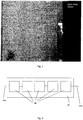
- Fig. 2 shows a schematic representation of how a recording of the in Fig. 1 surface of the semiconductor component 10 shown could look like.
- the break 46 in the pn junction 22 emerges clearly recognizable as an essentially one-dimensional decrease in intensity of the electroluminescent radiation of the cell (light areas 40).
- the break is shown accordingly as a black line.
- the break 46 runs in a (non-active) layer arranged below the pn junction 22 and this break has a negative effect on the crystal structure in the pn junction 22, so that a break in one does not -active layer can be detected with the proposed approach.
- These abrupt, essentially one-dimensional changes in intensity very easily allow defects to be automatically recognized by current image processing systems.
- the method proposed here also enables the electrical effects associated with a break to be detected.
- the entire area 42 is electrically impaired by the break and is characterized by reduced electroluminescence.
- area 44 this is only the case for the area below the break 46.
- the radiation behavior of the solar cell arrangement can be optically analyzed in a simple manner, so that direct, unambiguous and reproducible conclusions can be drawn about defects in the solar cell arrangement.
- Fig. 3 represents an exemplary photo of such an electroluminescent image of a silicon solar cell, in which a corresponding voltage was applied to operate the respective pn junctions in the forward direction.
- I 1500 mA
- t 2 s.
- FIG. 4 shows a plurality of solar cell arrangements 50 combined to form a string, each of which consists, for example, of a semiconductor component 10, as shown in FIG Fig. 1 is shown.
- the individual solar cell arrangements 20 are connected in series via their electrodes 51a and 51b.
- the solar cell arrangements 50 are applied to a common carrier 52. If a voltage is now applied to this entire string which, with n solar cell arrangement 50, is n times the voltage in order to switch a solar cell arrangement 50 in the forward direction, then the entire string of solar cells can be tested in one operation.
- Fig. 5 shows schematically a circuit diagram with the essential functionalities of a possible embodiment of the image processing unit 30 in detail.
- This image processing unit 30 has an image data storage area 60 for storing a radiation image of the semiconductor layer 10 (or the pn junction 22), a program storage area 62 containing an image processing program designed to automatically examine the radiation image for abrupt, essentially one-dimensional changes in intensity Identification of the detected changes in intensity as mechanical defects of the semiconductor component and a second program memory area 64 containing a program for analyzing the radiation image on the electrical effects of the mechanical defects.
- the two programs can be executed by a computer unit 66 which is connected to the individual memory areas 60 to 64 in terms of data technology.
- Fig. 6 shows a flow chart of an embodiment of the method according to the invention.
- a voltage is applied to a pn junction of the semiconductor component (with at least one pn junction in a semiconductor material with an indirect band transition) in the forward direction of the pn junction.
- the radiation behavior of the semiconductor layer generated by the applied voltage in the case of a Si semiconductor component is filtered at least for partial areas of the semiconductor layer by means of an infrared filter in such a way that electromagnetic radiation in the spectral range with a wavelength lower than infrared is blocked.
- an infrared filter in such a way that electromagnetic radiation in the spectral range with a wavelength lower than infrared is blocked.
- other filter combinations can be useful.
- the filtered radiation behavior is then optically recorded in a third method step 74, for example by means of a CCD camera.
- the detected radiation behavior is evaluated in a final method step 76a, the radiation behavior of the semiconductor layer being automatically examined for abrupt, essentially one-dimensional changes in intensity along the semiconductor layer and detected changes in intensity being identified as mechanical defects in the semiconductor component (method step 78).
- the integral over the radiation intensity of at least a first partial region of a first semiconductor layer can be determined automatically, then the integral over the radiation intensity of at least one comparison region of the same semiconductor layer or a second semiconductor layer can be determined and based on the result of an automatic comparison of the two Integrals of the first sub-area are identified as defective or as free from defects (method step 78).
- a conventional CCD camera such as the commercially available Si-CCD camera Sony XCD-SX910
- the selected parameters enable good compatibility of the process with the requirements of production: the selected current range is uncritical for the cell and does not damage it.
- the exposure times of 1-2 s ensure a quick inspection of all cells.
- the camera uses a standard Si-CCD detector and is therefore inexpensive, especially since no additional measures, such as cooling the camera, are required. Visible ambient light is blocked by the infrared filter, only shading from direct incident light on the cell can take place.
Landscapes
- Health & Medical Sciences (AREA)
- Biochemistry (AREA)
- Physics & Mathematics (AREA)
- Life Sciences & Earth Sciences (AREA)
- Chemical & Material Sciences (AREA)
- Analytical Chemistry (AREA)
- General Health & Medical Sciences (AREA)
- General Physics & Mathematics (AREA)
- Immunology (AREA)
- Pathology (AREA)
- Nuclear Medicine, Radiotherapy & Molecular Imaging (AREA)
- Photovoltaic Devices (AREA)
- Investigating Materials By The Use Of Optical Means Adapted For Particular Applications (AREA)
Description
Die vorliegende Erfindung betrifft ein Verfahren zur Detektion mechanischer Defekte eines Halbleiter-Bauelements, insbesondere einer Solarzelle oder Solarzellen-Anordnung, gemäß Anspruch 1 und eine entsprechende Anordnung gemäß Anspruch 11, sowie die Verwendung gemäß Anspruch 14.The present invention relates to a method for detecting mechanical defects of a semiconductor component, in particular a solar cell or solar cell arrangement, according to claim 1 and a corresponding arrangement according to claim 11, as well as the use according to
Vor allem bei Solargeneratoren für Satelliten kommt der Detektion mechanischer Defekte in den verwendeten Solarzellen vor dem Einsatz im Orbit eine große Bedeutung zu. Mechanische Defekte bzw. Zellfehler, wie Brüche, können nämlich hauptsächlich bedingt durch die Thermalzyklen im Orbit (90 Eclipsephasen pro Jahr in einem geostationären Orbit) weiter wachsen und sich extrem negativ auf die Zuverlässigkeit der Solargeneratoren auswirken. Angestrebt wird daher eine 100-% Kontrolle der Zellen auf mechanische Defekte, vor einer Auslieferung als auch über alle Produktionsschritte hinweg, um defekte Zellen möglichst frühzeitig austauschen zu können, und um zu vermeiden, dass defekte Zellen in einem Solargenerator verwendet werden. Dies gilt selbstverständlich auch für terrestrische Solarzellen und Module, auch wenn diese im Unterschied zu den Solarzellen eines Satelliten im Orbit leichter ausgetauscht werden können.In the case of solar generators for satellites in particular, the detection of mechanical defects in the solar cells used before they are used in orbit is of great importance. Mechanical defects or cell defects such as breaks can namely continue to grow due to the thermal cycles in orbit (90 eclipse phases per year in a geostationary orbit) and have an extremely negative effect on the reliability of the solar generators. The aim is therefore a 100% control of the cells for mechanical defects, both before delivery and across all production steps, in order to be able to replace defective cells as early as possible and to avoid defective cells from being used in a solar generator. Of course, this also applies to terrestrial solar cells and modules, even if, in contrast to the solar cells of a satellite in orbit, they can be exchanged more easily.
Derzeit werden mechanische Zellfehler in Solarzellen aus indirekten Halbleitern wie Silizium durch eine visuelle Zellinspektion detektiert. Ein trainiertes Auge kann durch Betrachten der Solarzellen unter geeigneten Beleuchtungsbedingungen Zellfehler im gespiegelten Licht anhand von Lichteffekten erkennen, die durch einen leichten Höhenversatz entlang des Zellbruchs hervorgerufen werden. Da die visuelle Zellinspektion zeitaufwendig und entsprechend teuer ist, werden Anstrengungen unternommen, dieses Verfahren zu automatisieren, beispielsweise durch eine phasenmessende Deflektrometrie. Es wurde auch schon versucht, externes Licht anderer Wellenlängen zu verwenden, um eine größere Eindringtiefe zu erzielen, oder Brüche anhand ihres Einflusses auf die Ausbreitung von Wärme zu detektieren, beispielsweise mittels thermografischer Verfahren. Eine Übersicht über die Detektion mechanischer Defekte in Solarzellen findet sich in der Veröffentlichung "
Die
In der Veröffentlichung "
Eine Aufgabe der vorliegenden Erfindung ist es nun, eine Möglichkeit zur Detektion von Defekten in Halbleiter-Bauelementen mit indirektem Halbleitermaterial, beispielsweise Silizium-basierten Solarzellen oder Solarzellen-Anordnungen, bereitzustellen.It is an object of the present invention to provide a possibility for the detection of defects in semiconductor components with indirect semiconductor material, for example silicon-based solar cells or solar cell arrangements.
Diese Aufgabe wird durch ein Verfahren zur Detektion mechanischer Defekte eines Halbleiter-Bauelements, insbesondere einer Solarzelle oder Solarzellen-Anordnung, mit den Merkmalen von Anspruch 1 und durch eine entsprechende Anordnung mit den Merkmalen von Anspruch 11 gelöst.This object is achieved by a method for detecting mechanical defects in a semiconductor component, in particular a solar cell or solar cell arrangement, with the features of claim 1 and by a corresponding arrangement with the features of claim 11.
Weitere Ausgestaltungen der Erfindung ergeben sich aus den abhängigen Ansprüchen.Further refinements of the invention emerge from the dependent claims.
Die vorliegende Erfindung basiert auf der Erkenntnis, dass auch indirekte Halbleiter wie Silizium unter bestimmten Bedingungen ein auswertbares Strahlungsverhalten besitzen. Aus der Veröffentlichung "
Mit der Erfindung können daher mechanische Defekte in einem HalbleiterBauelement mit einem pn-Übergang, das auf einem indirekten Halbleitermaterial wie beispielsweise Silizium basiert, dadurch detektiert werden, dass eine Spannung an diesem Halbleiter-Bauelement in Durchlassrichtung des pn-Übergangs angelegt werden kann, wodurch das Halbleiter-Bauelement zur Abgabe von elektromagnetischer Strahlung angeregt wird. Auf Grund des indirekten Bandübergangs ist die auftretende Elektrolumineszenz um Größenordnungen schwächer als in direkten Halbleitern und daher ist zur optischen Erfassung der von den aktiven Schichten im Halbleiter emittierten Strahlung ein geeigneter optischer Sensor, wie z.B. eine CCD Kamera notwendig. Diese muß an den Wellenlängenbereich der emittierten Strahlung angepasst sein und über eine angemessene Beobachtungszeit integriert, eine geeignete Empfindlichkeit besitzen. Für Halbleiter die auf Si oder Ge basieren und von großer praktische Relevanz sind liegt die emittierte Strahlung im infraroten Wellenlängenbereich. In diesem Fall kann durch einen Infrarotfilter sämtliches sichtbares Licht ausgeblendet werden, wodurch auch relativ unempfindlichere Detektoren verwendet werden können und die Defekt-Detektion unter Umgebungslicht möglich wird. Im allgemeineren Fall können geeignete (Bandpass)filter dazu verwendet werden, die Strahlung eines bestimmten pn Übergangs zu isolieren und nur diese Halbleiterschichten auf Defekte zu überprüfen. Unter optischer Erfassung im Sinne der vorliegenden Erfindung ist dabei insbesondere die Ortsauflösung der Detektion der vom Halbleiter-Bauelement emittierten elektromagnetischen Strahlung zu verstehen.With the invention, therefore, mechanical defects in a semiconductor component with a pn junction based on an indirect semiconductor material such as silicon can be detected by applying a voltage to this semiconductor component in the forward direction of the pn junction Semiconductor component is excited to emit electromagnetic radiation. Due to the indirect band transition, the electroluminescence that occurs is orders of magnitude weaker than in direct semiconductors and therefore a suitable optical sensor, such as a CCD camera, is necessary for optical detection of the radiation emitted by the active layers in the semiconductor. This must be adapted to the wavelength range of the emitted radiation and integrated over an appropriate observation time and have a suitable sensitivity. For semiconductors based on Si or Ge and of great practical relevance, the emitted radiation is in the infrared wavelength range. In this case, an infrared filter can do everything visible light are masked out, whereby relatively less sensitive detectors can be used and the defect detection under ambient light is possible. In the more general case, suitable (bandpass) filters can be used to isolate the radiation from a specific pn junction and only check these semiconductor layers for defects. In the context of the present invention, optical detection is to be understood in particular as the spatial resolution of the detection of the electromagnetic radiation emitted by the semiconductor component.
Die Analyse des Strahlungsverhaltens erfolgt dabei derart, dass das Strahlungsverhalten der Halbleiterschicht auf abrupte, im wesentlichen eindimensionale Intensitätsänderungen entlang der Halbleiterschicht untersucht wird und die detektierten Intensitätsänderungen als mechanische Defekte des Halbleiter-Bauelements gekennzeichnet werden. Eine solche Analyse kann automatisch durch entsprechende Bildverarbeitungssysteme oder Strahlungsintensitätsdetektoren erfolgen. Es wird also hier nicht lediglich qualitativ das globale Strahlungsverhalten betrachtet (Strahlung vorhanden oder nicht vorhanden), sondern es wird lokal der Intensitätsverlauf des Strahlungsverhaltens entlang des Bauelements bzw. entlang der Halbleiterschicht mit indirektem Bandübergang untersucht. Auf diese Weise können lokale Defekte erkannt werden, die die Funktionsfähigkeit des Bauelements in gewissen Teilbereichen beeinträchtigen oder in sonstiger Weise stören können. Eine abrupte, im wesentlichen eindimensional ausgedehnte Intensitätsänderung lässt auf einen mechanischen Defekt wie einen Bruch einer Halbleiterschicht schließen.The radiation behavior is analyzed in such a way that the radiation behavior of the semiconductor layer is examined for abrupt, essentially one-dimensional changes in intensity along the semiconductor layer and the detected changes in intensity are identified as mechanical defects in the semiconductor component. Such an analysis can be carried out automatically by appropriate image processing systems or radiation intensity detectors. The global radiation behavior is not only considered qualitatively here (radiation present or not present), but the intensity profile of the radiation behavior along the component or along the semiconductor layer with an indirect band transition is examined locally. In this way, local defects can be detected which impair the functionality of the component in certain subregions or can interfere in some other way. An abrupt, essentially one-dimensionally extended change in intensity suggests a mechanical defect such as a break in a semiconductor layer.
Grundsätzlich kann das Verfahren aber auch angewendet werden, um lokale Eintrübungen, Degradationen oder ähnliches, beispielsweise in Deckelgläsern und Deckschichten von Solarzellen oder ähnliches zu detektieren. Diese können sich dann aber beispielsweise als Intensitätsänderung zweidimensionaler Ausdehnung im Strahlungsverhalten auswirken und entsprechend detektierbar sein.In principle, however, the method can also be used to detect local cloudiness, degradation or the like, for example in cover glasses and cover layers of solar cells or the like. However, these can then have an effect, for example, as a two-dimensional change in intensity in the radiation behavior and can be detected accordingly.
Die vorliegende Erfindung bietet den Vorteil, dass eine wesentliche Verbesserung der Detektion mechanischer Fehler in planaren Halbleiter-Bauelementen möglich ist, die insbesondere aus einem Halbleitermaterial mit indirektem Bandübergang wie Silizium bestehen. Gegenüber der visuellen Zellinspektion, die insbesondere bei texturierten Silizium-Solarzellen an ihre Grenzen stößt, können Fehler zu nahezu 100 % erkannt werden (gegenüber einer visuellen Erkennungsrate von in der Regel weniger als 50 %). Weiterhin ist die Inspektion personenunabhängig und reproduzierbar und ermöglicht eine eindeutige Fehlerdokumentation. Zusätzlich bringt das Verfahren eine Zeitersparnis mit sich und lässt sich automatisieren.The present invention offers the advantage that a significant improvement in the detection of mechanical defects in planar semiconductor components is possible, which in particular consist of a semiconductor material with an indirect band transition such as silicon. Compared to the visual cell inspection, which reaches its limits, especially with textured silicon solar cells, errors can be detected almost 100% (compared to a visual detection rate of usually less than 50%). Furthermore, the inspection is person-independent and reproducible and enables clear error documentation. In addition, the process saves time and can be automated.
Gemäß einer Ausführungsform der Erfindung ist nun ein Verfahren zur Detektion mechanischer Defekte eines Halbleiter-Bauelements, insbesondere einer Solarzelle oder Solarzellen-Anordnung, mit zumindest einem pn-Übergang in einem Halbleitermaterial mit indirektem Bandübergang vorgesehen, wobei
- an den zumindest einen pn-Übergang eine Spannung zum Betrieb des pn-Übergangs in Durchlassrichtung angelegt wird,
- das durch die angelegte Spannung erzeugte Strahlungsverhalten der Halbleiterschicht zumindest für Teilbereiche der Halbleiterschicht mittels eines Filters derart selektiert werden kann, dass entweder nur die elektromagnetische Strahlung eines oder mehrerer pn Übergänge erfasst wird und/oder dass sämtliches sichtbares Umgebungslicht geblockt wird,
- das gefilterte Strahlungsverhalten, oder im Bedarfsfall auch das ungefilterte Strahlungsverhalten, optisch erfasst und ausgewertet wird, wobei
- automatisch das Integral über die Strahlungsintensität zumindest eines ersten Teilbereichs einer ersten Halbleiterschicht bestimmt wird, anschließend das Integral über die Strahlungsintensität zumindest eines Vergleichsbereichs derselben Halbleiterschicht oder einer zweiten Halbleiterschicht bestimmt wird und aufgrund des Ergebnisses eines automatischen Vergleichs der beiden Integrale der erste Teilbereich als defekt oder als defektfrei gekennzeichnet wird.
- a voltage for operating the pn junction in the forward direction is applied to the at least one pn junction,
- the radiation behavior of the semiconductor layer generated by the applied voltage can be selected at least for partial areas of the semiconductor layer by means of a filter in such a way that either only the electromagnetic radiation of one or more pn junctions is detected and / or that all visible ambient light is blocked,
- the filtered radiation behavior, or if necessary also the unfiltered radiation behavior, is optically recorded and evaluated, whereby
- the integral over the radiation intensity of at least a first sub-area of a first semiconductor layer is automatically determined, then the integral over the radiation intensity of at least one comparison area of the same semiconductor layer or a second semiconductor layer is determined and, based on the result of an automatic comparison of the two integrals, the first sub-area is defined as defective or as is marked defect-free.
Gemäß einer weiteren Ausführungsform der vorliegenden Erfindung kann beim optischen Erfassen ein Abschatten von direktem Auflicht auf eine Oberfläche des Halbleiter-Bauelements erfolgen. Dies bietet den Vorteil, dass lediglich elektromagnetische Strahlung erfasst und ausgewertet wird, die von dem Halbleiter-Bauelement emittiert wird, an dem die Durchlassspannung angelegt ist. Vom Bauteil reflektierte elektromagnetische Strahlung, die beispielsweise durch seitlich auf die Oberfläche des Halbleiter-Bauelements einfallendes Licht erzeugt wird, kann hierdurch vermieden werden.According to a further embodiment of the present invention, a shadowing of direct incident light on a surface of the semiconductor component can take place during optical detection. This offers the advantage that only electromagnetic radiation is detected and evaluated which is emitted by the semiconductor component to which the forward voltage is applied. Electromagnetic radiation reflected by the component, which is generated, for example, by light incident laterally on the surface of the semiconductor component, can thereby be avoided.
Gemäß einer weiteren Ausführungsform der Erfindung kann das optische Erfassen innerhalb einer Zeitspanne von höchstens zwei Sekunden erfolgen. Es hat sich gezeigt, dass eine derartige Zeitspanne zur Aufnahme hochauflösender Bilder des auf Si basierenden Halbleiter-Bauelements für eine weitere Auswertung zur Detektion mittels einer herkömmlichen Si-CCD-Kamera geeignet ist.According to a further embodiment of the invention, the optical detection can take place within a time span of at most two seconds. It has been shown that such a time span for recording high-resolution images of the Si-based semiconductor component is suitable for further evaluation for detection by means of a conventional Si-CCD camera.
Gemäß einer weiteren Ausführungsform der Erfindung kann zudem eine Spannung zum Betrieb des pn-Übergangs in Durchlassrichtung angelegt werden, die einen Strom in einem Bereich des ein- bis zweifachen einer Kurzschluss-Stromstärke des Halbleiter-Bauelements bewirkt. Auch hier hat sich gezeigt, dass eine derartige Spanne zur Aufnahme hochauflösender Bilder des auf Si basierenden Halbleiter-Bauelements für eine weitere Auswertung zur Detektion mittels einer herkömmlichen Si-CCD-Kamera geeignet ist.According to a further embodiment of the invention, a voltage can also be applied to operate the pn junction in the forward direction, which voltage causes a current in a range of one to two times a short-circuit current intensity of the semiconductor component. Here, too, it has been shown that such a range for recording high-resolution images of the Si-based semiconductor component is suitable for further evaluation for detection by means of a conventional Si-CCD camera.
Gemäß einer Ausführungsform der Erfindung kann das Halbleitermaterial mit indirektem Bandübergang Silizium, insbesondere polykristallines Silizium, umfassen.According to one embodiment of the invention, the semiconductor material with an indirect band transition can comprise silicon, in particular polycrystalline silicon.
Ferner kann gemäß einer weiteren Ausführungsform der vorliegenden Erfindung eine indirekte Detektion mechanischer Defekte einer strahlungsinaktiven Schicht des Halbleiter-Bauelements erfolgen, wobei das Strahlungsverhalten einer benachbarten strahlungsaktiven Halbleiterschicht automatisch auf abrupte, im wesentlichen eindimensional ausgedehnte Intensitätsänderungen längs der Halbleiterschicht untersucht wird und detektierte Intensitätsänderungen als mechanische Defekte der strahlungsinaktiven Schicht des Halbleiter-Bauelements gekennzeichnet werden. Insbesondere bei Tandem-Solarzellen (oder Solarzellen mit zwei oder mehreren aktiven Schichten) kann durch eine derartige Ausführungsform der vorliegenden Erfindung ein Bruch oder eine Degradationen von einer nicht-strahlenden Schicht des Halbleiter-Bauelements ebenfalls mittels des erfindungsgemäßen Ansatzes erkannt werden, da das Strahlungsverhalten des Halbleiter-Bauelements auch von diesem Bruch oder der Degradationen in der nicht-strahlenden Schicht beeinflusst wird.Furthermore, according to a further embodiment of the present invention, an indirect detection of mechanical defects of a radiation-inactive layer of the semiconductor component can take place, the radiation behavior of an adjacent radiation-active semiconductor layer being automatically examined for abrupt, essentially one-dimensionally extended intensity changes along the semiconductor layer and detected intensity changes as mechanical defects the radiation-inactive layer of the semiconductor component can be identified. In particular in the case of tandem solar cells (or solar cells with two or more active layers), such an embodiment of the present invention can also detect a breakage or degradation of a non-radiating layer of the semiconductor component using the approach according to the invention, since the radiation behavior of the Semiconductor component is also influenced by this breakage or the degradations in the non-radiative layer.
Außerdem kann gemäß einer weiteren Ausführungsform der Erfindung eine kombinierte Detektion von mechanischen Defekten und Erfassung der elektrischen Auswirkungen der mechanischen Defekte erfolgen, wobei eine Analyse des Strahlungsverhaltens des Bauelements in einem ersten Wellenlängenbereich der Detektion mechanischer Defekte und eine Analyse des Strahlungsverhaltens des Bauelements in einem zweiten Wellenlängenbereich der Erfassung der elektrischen Auswirkungen zu Grunde gelegt wird. Hierdurch lässt sich vorteilhaft ausnutzen, dass auch nicht-aktive Schichten das Strahlungsverhalten des Halbleiter-Bauelements beeinflussen und somit auch durch die Analyse des Strahlungsverhaltens des Halbleiter-Bauelements diese nicht-aktiven Schichten auf mechanische Defekte untersucht werden können.In addition, according to a further embodiment of the invention, a combined detection of mechanical defects and detection of the electrical effects of the mechanical defects can take place, with an analysis of the radiation behavior of the component in a first wavelength range of the detection of mechanical defects and an analysis of the radiation behavior of the component in a second wavelength range the recording of the electrical effects is taken as a basis. This advantageously makes use of the fact that non-active layers also influence the radiation behavior of the semiconductor component and thus these non-active layers can also be examined for mechanical defects by analyzing the radiation behavior of the semiconductor component.
Gemäß einer weiteren Ausführungsform der vorliegenden Erfindung kann eine Mehrzahl von n Halbleiter-Bauelementen in einer Serienschaltung und/oder Parallelschaltung auf einem gemeinsamen Bauelemente-Träger angeordnet sein und an die Gesamtheit der Halbleiter-Bauelemente eine Spannung angelegt werden, die in Serienschaltung dem n-fachen der Spannung und in Parallelschaltung dem n-fachen Strom zum Betrieb eines Bauelementes in Durchlassrichtung entspricht. Dadurch können insbesondere bereits vormontierte Solarzellen-Panels oder -Module mit mehreren einzelnen in Reihe geschalteten Zellen inspiziert werden.According to a further embodiment of the present invention, a plurality of n semiconductor components can be arranged in a series connection and / or parallel connection on a common component carrier and a voltage which is n times the value in series connection can be applied to the entirety of the semiconductor components corresponds to the voltage and, in parallel connection, the n-fold current for operating a component in the forward direction. In this way, in particular, already preassembled solar cell panels or modules with several individual cells connected in series can be inspected.
Gemäß einer weiteren Ausführungsform der Erfindung kann eine Anordnung zur Detektion mechanischer Defekte eines Halbleiter-Bauelements, insbesondere einer Solarzelle oder Solarzellen-Anordnung, vorgesehen sein mit zumindest einem pn-Übergang in einem Halbleitermaterial mit indirektem Bandübergang und mindestens einer Elektrode, die mit dem p-leitenden Bereich des Halbleiter-Bauelements verbunden ist und mindestens einer Elektrode, die mit dem n-leitenden Bereich des Halbleiter-Bauelements verbunden ist, mit:
- Spannungsversorgungsanschlüssen, die mit den Elektroden des HalbleiterBauelements verbunden sind, um eine Spannungsversorgung zum Betrieb des pn-Übergangs in Durchlassrichtung zu ermöglichen,
- einer Einrichtung zur optischen Erfassung und Auswertung des durch eine angelegte Spannung erzeugte Strahlungsverhalten der Halbleiterschicht zumindest für Teilbereiche der Halbleiterschicht, wobei die Anordnung folgende Merkmale umfasst:
- eine Filtereinheit, die so gewählt wird, nur die Strahlung einer oder mehrerer pn Übergänge zu detektieren und/oder sichtbares Umgebungslicht zu blockieren,
- einen Bilddaten-Speicherbereich zur Speicherung eines Strahlungsbildes einer Halbleiterschicht,
- mindestens eines der Strahlungsbilder auf abrupte, im wesentlichen eindimensional ausgedehnte Intensitätsänderungen und zur Kennzeichnung der detektierten Intensitätsänderungen als mechanische Defekte des Halbleiter-Bauelements und
- einen zweiten Programm-Speicherbereich enthaltend ein Programm zur Analyse mindestens eines der Strahlungsbilder auf elektrische Auswirkungen der mechanischen Defekte.
- Voltage supply connections that are connected to the electrodes of the semiconductor component in order to enable a voltage supply to operate the pn junction in the forward direction,
- a device for the optical detection and evaluation of the radiation behavior of the semiconductor layer generated by an applied voltage, at least for partial areas of the semiconductor layer, the arrangement comprising the following features:
- a filter unit that is chosen to only detect the radiation from one or more pn junctions and / or to block visible ambient light,
- an image data storage area for storing a radiation image of a semiconductor layer,
- at least one of the radiation images for abrupt, essentially one-dimensionally extended changes in intensity and for identifying the detected changes in intensity as mechanical defects of the semiconductor component and
- a second program memory area containing a program for analyzing at least one of the radiation images for electrical effects of the mechanical defects.
Die Einrichtung zur optischen Erfassung umfasst ferner eine Einrichtung zum Abschatten von direktem Auflicht auf eine Oberfläche des Halbleiter-Bauelements, da die Detektion der vom Halbleiter-Bauelement emittierten Strahlung durch Reflexionen von seitlich auf eine Oberfläche des Halbleiter-Bauelements einfallenden Lichts negative beeinflusst werden kann.The device for optical detection further comprises a device for shading direct incident light on a surface of the semiconductor component, since the detection of the radiation emitted by the semiconductor component can be negatively influenced by reflections of light incident laterally on a surface of the semiconductor component.
Ferner kann auch in einer weiteren Ausführungsform der vorliegenden Erfindung die Einrichtung zum optischen Erfassen ausgebildet sein, das optische Erfassen innerhalb einer Zeitspanne von höchstens zwei Sekunden durchzuführen.Furthermore, in a further embodiment of the present invention, the device for optical detection can also be designed to carry out the optical detection within a time span of at most two seconds.
Gemäß einer weiteren Ausführungsform der Erfindung kann die Spannungsversorgung ausgebildet sein, um über die Spannungsversorgungsanschlüsse eine Spannung zum Betrieb des pn-Übergangs in Durchlassrichtung anzulegen, die einen Strom in einem Bereich des etwa ein- bis zweifachen einer Kurzschluss-Stromstärke des Halbleiter-Bauelements bewirkt.According to a further embodiment of the invention, the voltage supply can be designed to apply a voltage for operating the pn junction in the forward direction via the voltage supply connections, which voltage causes a current in a range of approximately one to two times a short-circuit current intensity of the semiconductor component.
Schließlich ist gemäß einer Ausführungsform der Erfindung die Verwendung einer Anordnung nach der Erfindung zur insbesondere automatischen Detektion mechanischer Defekte von Solarzellen-Anordnungen vorgesehen.Finally, according to one embodiment of the invention, the use of an arrangement according to the invention for the particularly automatic detection of mechanical defects in solar cell arrangements is provided.
Weitere Vorteile und Anwendungsmöglichkeiten der vorliegenden Erfindung ergeben sich aus der nachfolgenden Beschreibung in Verbindung mit den in den Zeichnungen dargestellten Ausführungsbeispielen.Further advantages and possible applications of the present invention emerge from the following description in conjunction with the exemplary embodiments shown in the drawings.
In der Beschreibung, in den Ansprüchen, in der Zusammenfassung und in den Zeichnungen werden die in der hinten angeführten Liste der Bezugszeichen verwendet Begriffe und zugeordneten Bezugszeichen verwendet.In the description, in the claims, in the abstract and in the drawings, the terms and assigned reference symbols used in the list of reference symbols given below are used.
Die Zeichnungen zeigen in:
- Fig. 1
- ein Diagramm eines prinzipiellen Aufbaus zur Detektion mechanischer Defekte in einem Halbleiter-Bauelement gemäß einem Ausführungsbeispiel der vorliegenden Erfindung;
- Fig. 2
- eine prinzipielle Darstellung des Strahlungsverhaltens eines defekten Halbleiter-Bauelements von dessen Oberfläche;
- Fig. 3
- ein beispielhaftes Foto einer defekten Silizium-Solarzelle unter Verwendung eines Ausführungsbeispiels des erfindungsgemäßen Ansatzes spricht.
- Fig. 4
- eine schematische Darstellung einer Anordnung von mehreren Solarzellen zu einem String gemäß einem Ausführungsbeispiel der vorliegenden Erfindung;
- Fig. 5
- eine schematische Darstellung einer Bildverarbeitungseinrichtung; und
- Fig. 6
- ein Ablaufdiagramm eines Ausführungsbeispiels des erfindungsgemäßen Verfahrens.
- Fig. 1
- a diagram of a basic structure for the detection of mechanical defects in a semiconductor component according to an embodiment of the present invention;
- Fig. 2
- a basic representation of the radiation behavior of a defective semiconductor component from its surface;
- Fig. 3
- an exemplary photo of a defective silicon solar cell using an embodiment of the inventive approach speaks.
- Fig. 4
- a schematic representation of an arrangement of several solar cells to form a string according to an embodiment of the present invention;
- Fig. 5
- a schematic representation of an image processing device; and
- Fig. 6
- a flowchart of an embodiment of the method according to the invention.
Im Folgenden können gleiche und/oder funktional gleiche Elemente mit den gleichen Bezugszeichen versehen sein. Die im Folgenden angegebenen absoluten Werte und Maßangaben sind nur beispielhafte Werte und stellen keine Einschränkung der Erfindung auf derartige Dimensionen dar.In the following, identical and / or functionally identical elements can be provided with the same reference symbols. The absolute values and dimensions given below are only exemplary values and do not restrict the invention to such dimensions.
In
Ferner zeigt
Wird nun für das Halbleiter-Bauelement 10 eine Solarzellenanordnung verwendet, so kann ein technischer Effekt verwendet werden, gemäß dem eine Solarzelle nicht nur Strom bei Lichteinfall erzeugt, sondern auch elektromagnetische Strahlung abgibt (bzw. Elektrolumineszenz auftritt), wenn eine Spannung 23 zwischen der oberen Elektrode 12 und der unteren Elektrode 14 derart angelegt wird, dass der pn-Übergang 22 im Durchlassrichtung betrieben wird. Dieser Effekt tritt zwar vor allem bei der Verwendung von Halbleitermaterialien mit direktem Bandübergang auf (strahlende Rekombination der Ladungsträger), jedoch konnte auch festgestellt werden, dass in Materialien mit indirektem Bandübergang eine (wesentlich schwächere) Elektrolumineszenz auftritt, deren Intensität proportional zur Minoritätsträgerdiffusionslänge ist.If a solar cell arrangement is now used for the
Brüche bzw. Defekte im Halbleiterbauelement beeinflussen zwar auch die Minoritätsträgerdiffusionslänge. Für das hier vorgeschlagene Verfahren ist aber insbesondere entscheidend, dass Brüche bzw. Defekte als Stromsenken wirken und, verbunden mit der Querleitfähigkeit der Zelle, die laterale Stromverteilung und damit die räumliche Verteilung der Elektrolumineszenz der Zelle makroskopisch beeinflussen, wie in der Veröffentlichung "
Bei den auf Si und Ge basierenden Halbleiterbauelementen ist anzumerken, dass diese Elektrolumineszenz im infraroten Spektralbereich (d.h. elektromagnetische Strahlung mit mehr als 800 nm Wellenlänge) erfolgt. Um daher elektromagnetische Strahlung anderer Spektralbereiche auszublenden, wird bei der Aufnahmeeinheit 24 ein Infrarotfilter 26 verwendet, um die Empfindlichkeit des Aufnahmesensors 28, der beispielsweise wie in
Die Aufnahmeeinheit 28 kann optional auch mit anderen Filterkombinationen versehen werden, um selektiv die Elektrolumineszenz eines oder mehrerer pn Übergange zu detektieren.The
Die
Zusammenfassend ist anzumerken, dass beispielsweise mittels einer herkömmlichen CCD-Kamera (wie der kommerziell erhältlichen Si-CCD-Kamera Sony XCD-SX910) und eines Infrarotfilters gezeigt werden konnte, dass durch Anlegen eines Stroms, beispielsweise in der Größenordnung von 1-2 x Isc (= Kurzschlussstrom der Zelle) und Belichtungszeiten von 1-2 s hochauflösende Bilder der Zellbrüche in Silizium-Solarzellen gemacht werden können, wie aus
- 1010
- Halbleiter-BauelementSemiconductor component
- 1212th
- obere Elektrodeupper electrode
- 1414th
- untere Elektrodelower electrode
- 1616
- HalbleitermaterialSemiconductor material
- 1818th
- n-dotierte Schichtn-doped layer
- 2020th
- p-dotierte Schichtp-doped layer
- 2222nd
- pn-Übergangpn junction
- 2323
- Spannung V zum Betreiben des Halbleiter-Bauelements in DurchlassrichtungVoltage V for operating the semiconductor component in the forward direction
- 2424
- AufnahmeeinheitRecording unit
- 2626th
- Infrarot-FilterInfrared filter
- 2828
- optischer Sensor, CCD-Kameraoptical sensor, CCD camera
- 3030th
- AuswerteeinheitEvaluation unit
- 3232
- seitliche Blendenside panels
- 3434
- seitliches Licht, Auflichtlateral light, incident light
- 40,40,
- lumineszierende Oberflächenbereiche des HalbleiterBauelementsluminescent surface areas of the semiconductor component
- 42, 4442, 44
- Bereiche des Halbleiters mit verminderter ElektrolumineszenzAreas of the semiconductor with reduced electroluminescence
- 4646
- Bruch, mechanischer DefektBreakage, mechanical defect
- 5050
- Halbleiter-Bauelemente in Modul-AnordnungSemiconductor components in a module arrangement
- 51a, 51b51a, 51b
- Anschlusselektroden des ModulsConnection electrodes of the module
- 5252
- Bauelemente-TrägerComponent carrier
- 6060
- Bilddaten-SpeicherbereichImage data storage area
- 6262
- erster Programm-Speicherbereichfirst program memory area
- 6464
- zweiter Programm-Speicherbereichsecond program memory area
- 6666
- RechnereinheitComputing unit
- 7070
- Schritt des Anlegens einer Spannung an das HalbleiterBauelementStep of applying a voltage to the semiconductor device
- 7272
- Schritt des Filterns des Strahlungsverhaltens mittels eines Infrarot-FiltersStep of filtering the radiation behavior by means of an infrared filter
- 7474
- Erfassen des gefilterten StrahlungsverhaltensDetection of the filtered radiation behavior
- 76a76a
- Untersuchen des erfassten Strahlungsverhaltens auf abrupte, im wesentlichen eindimensionale IntensitätsänderungenExamination of the recorded radiation behavior for abrupt, essentially one-dimensional changes in intensity
- 76b76b
- Automatisches Bestimmen eines Integrals über die Strahlungsintensität zumindest eines ersten Teilbereichs einer ersten Halbleiterschicht und anschließend des Integrals über die Strahlungsintensität zumindest eines Vergleichsbereichs derselben Halbleiterschicht oder einer zweiten HalbleiterschichtAutomatic determination of an integral over the radiation intensity of at least a first partial region of a first semiconductor layer and then the integral over the radiation intensity of at least one comparison region of the same semiconductor layer or of a second semiconductor layer
- 7878
- Kennzeichnen von detektierten Intensitätsänderungen als mechanische Defekte des Halbleiter-Bauelements oder Kennzeichnen des ersten Teilbereichs als defekt oder als defektfrei aufgrund eines Ergebnisses eines automatischen Vergleichs der beiden IntegraleIdentification of detected changes in intensity as mechanical defects of the semiconductor component or identification of the first sub-area as defective or as defect-free on the basis of a result of an automatic comparison of the two integrals
Claims (14)
- A method for detecting mechanical defects of a Silicon or Germanium based semiconductor device (10), in particular a solar cell or solar cell arrangement, having at least one pn-junction (22) in a semiconductor layer formed of a semiconductor material (16) with an indirect band junction, wherein- a voltage (23) is applied (70) to the at least one pn-junction (22) for operating the pn-junction (22) in a transmitting direction,- the radiation behavior of the semiconductor layer generated by the applied voltage (23) is optically detected (74) and analyzed (76) at least for partial regions of the semiconductor layer, wherein- the radiation behavior of the semiconductor layer is automatically examined (76a) for abrupt, substantially one-dimensional changes of intensity along the semiconductor layer, and detected changes of intensity are identified (78) as mechanical defects (46) of the semiconductor device (10),characterized in that
an infrared filter (26) is used (72) for optically detecting the radiation behavior of the semiconductor layer, so that electromagnetic radiation in the spectral range with a wavelength lower than infrared is blocked, and/or the electroluminescence of one or more pn-junctions is selected by means of filter combinations adapted to the semiconductor material. - The method according to claim 1, characterized in that the integral over the radiation intensity of at least a first partial region (44, 42) of a first semiconductor layer is automatically determined, subsequently the integral over the radiation intensity of at least one comparison region of the same semiconductor layer (44, 42) or of a second semiconductor layer (42, 40) is determined (76b), and on the basis of the result of an automatic comparison of the two integrals, the first partial region (44) is characterized (78) as defective or as defect-free.
- The method according to one of claims 1 or 2,
characterized in that
during optically detecting (74), shading of direct incident light (34) onto a surface of the semiconductor device (10) occurs. - The method according to any one of claims 1 to 3,
characterized in that
the optically detecting (74) takes place within a time period of no more than two seconds. - The method according to any one of claims 1 to 4,
characterized in that
a voltage (23) for operating the pn-junction (22) in the transmitting direction is applied, which causes a current in a range of about one to two times a short-circuit current intensity of the semiconductor device (10). - The method according to any one of claims 1 to 5,
characterized in that
the semiconductor material (16) with an indirect band junction comprises silicon, in particular polycrystalline silicon. - The method according to any one of claims 1 to 6,
characterized in that
an indirect detection of mechanical defects of a radiation-inactive layer of the semiconductor device (10) takes place, wherein the radiation behavior of an adjacent radiation-active semiconductor layer is automatically examined for abrupt, substantially one-dimensional changes of intensity along the semiconductor layer and detected changes of intensity are identifies as mechanical defects (46) of the radiation-inactive layer of the semiconductor device (10). - The method according to any one of claims 1 to 7,
characterized in that
a combined detection of mechanical defects (46) and detection of the electrical effects of the mechanical defects is performed, wherein an analysis of the radiation behavior of the semiconductor device (10) in a first wavelength range is used as a basis for the detection of mechanical defects and an analysis of the radiation behavior of the semiconductor device (10) in a second wavelength range is used as a basis for the detection of the electrical effects. - The method according to any one of claims 1 to 8,
characterized in that
a plurality of n semiconductor devices (50, 10) is arranged in series on a common device carrier (52), and a voltage corresponding to n times the voltage (23) for operating a semiconductor device (10) in the transmitting direction is applied to the entirety of the semiconductor devices (50, 10). - The method according to any one of claims 1 to 8,
characterized in that
a plurality of n semiconductor devices (10) is arranged in parallel on a common device carrier, and a voltage is applied to the entirety of the semiconductor devices (10) which causes n times the current to operate a semiconductor device (10) in the transmitting direction. - An arrangement for performing the method according to anyone of claims 1 to 10 for detecting mechanical defects of a Silicon or Germanium based semiconductor device (10), in particular a solar cell or solar cell arrangement, having at least one pn-junction (22) in a semiconductor layer of a semiconductor material (16) with an indirect band junction and at least one electrode (14) which is connected to the p-conducting region (20) of the semiconductor device (10) and at least one electrode (12) which is connected to the n-conducting region (18) of the semiconductor device (10), having:- voltage supply terminals connected to the electrodes (12, 14) of the semiconductor device (10) to enable a voltage supply (V, 23) to operate the pn-junction (22) in the transmitting direction,- a device (24) for optically detecting and evaluating the radiation behavior of the semiconductor layer generated by an applied voltage at least for partial regions of the semiconductor layer,- an image data storage area (60) for storing a radiation image of the semiconductor layer,- a first program memory area (62) containing an image processing program adapted to automatically examine the radiation image for abrupt, substantially one-dimensional changes of intensity and to identify the detected changes of intensity as mechanical defects (46) of the semiconductor device (10), and- a second program memory area (64) containing a program adapted to analyze the radiation image for electrical effects of the mechanical defects, wherein- the device (24) for optically detecting and evaluating the radiation behavior of the semiconductor layer generated by an applied voltage comprises a filter unit (26),characterized in that the filter unit is designed such that electromagnetic radiation in the spectral range with a wavelength lower than infrared is blocked and/or designed so as to isolate the radiation of one or more pn-transitions, that the device (24) for optically detecting comprises a device (34) for shading direct incident light onto a surface of the semiconductor device (10), and that the device (24) for optically detecting and evaluating is designed to detect the radiation behavior of the semiconductor layer of a semiconductor material with an indirect band junction.
- The arrangement according to claim 11,
characterized in that
the device (24) for optically detecting is designed to perform the optically detecting within a time period of no more than two seconds. - The arrangement according to any one of claims 11 or 12,
characterized in that
the voltage supply (V, 23) is adapted to apply, via the voltage supply terminals, a voltage (23) for operating the pn-junction (22) in the transmitting direction, which causes a current in a range of about one to two times a short-circuit current intensity of the semiconductor device (10). - Use of an arrangement according to anyone of claims 11 to 13 for performing the method according to anyone of claims 1 to 10 for detecting mechanical defects of a semiconductor device, in particular for automatically detecting mechanical defects of solar cell arrangements.
Priority Applications (1)
| Application Number | Priority Date | Filing Date | Title |
|---|---|---|---|
| EP19162255.4A EP3514523B1 (en) | 2007-02-09 | 2008-02-01 | Method for detecting mechanical defects in a semiconductor component, in particular a solar cell or solar cell arrangement |
Applications Claiming Priority (2)
| Application Number | Priority Date | Filing Date | Title |
|---|---|---|---|
| DE102007007140A DE102007007140B4 (en) | 2007-02-09 | 2007-02-09 | Method and arrangement for detecting mechanical defects of a semiconductor device, in particular a solar cell or solar cell arrangement |
| PCT/DE2008/000180 WO2008095467A1 (en) | 2007-02-09 | 2008-02-01 | Method and arrangement for detecting mechanical defects in a semiconductor component, in particular a solar cell or solar cell arrangement |
Related Child Applications (2)
| Application Number | Title | Priority Date | Filing Date |
|---|---|---|---|
| EP19162255.4A Division-Into EP3514523B1 (en) | 2007-02-09 | 2008-02-01 | Method for detecting mechanical defects in a semiconductor component, in particular a solar cell or solar cell arrangement |
| EP19162255.4A Division EP3514523B1 (en) | 2007-02-09 | 2008-02-01 | Method for detecting mechanical defects in a semiconductor component, in particular a solar cell or solar cell arrangement |
Publications (2)
| Publication Number | Publication Date |
|---|---|
| EP2115435A1 EP2115435A1 (en) | 2009-11-11 |
| EP2115435B1 true EP2115435B1 (en) | 2021-05-05 |
Family
ID=39345425
Family Applications (2)
| Application Number | Title | Priority Date | Filing Date |
|---|---|---|---|
| EP19162255.4A Active EP3514523B1 (en) | 2007-02-09 | 2008-02-01 | Method for detecting mechanical defects in a semiconductor component, in particular a solar cell or solar cell arrangement |
| EP08706845.8A Active EP2115435B1 (en) | 2007-02-09 | 2008-02-01 | Method and arrangement for detecting mechanical defects in a semiconductor component, in particular a solar cell or solar cell arrangement |
Family Applications Before (1)
| Application Number | Title | Priority Date | Filing Date |
|---|---|---|---|
| EP19162255.4A Active EP3514523B1 (en) | 2007-02-09 | 2008-02-01 | Method for detecting mechanical defects in a semiconductor component, in particular a solar cell or solar cell arrangement |
Country Status (4)
| Country | Link |
|---|---|
| US (1) | US8306309B2 (en) |
| EP (2) | EP3514523B1 (en) |
| DE (1) | DE102007007140B4 (en) |
| WO (1) | WO2008095467A1 (en) |
Families Citing this family (12)
| Publication number | Priority date | Publication date | Assignee | Title |
|---|---|---|---|---|
| JP4153021B1 (en) * | 2007-10-22 | 2008-09-17 | 日清紡績株式会社 | Solar cell inspection equipment |
| US20100073011A1 (en) * | 2008-09-23 | 2010-03-25 | Applied Materials, Inc. | Light soaking system and test method for solar cells |
| KR101055790B1 (en) | 2009-04-17 | 2011-08-09 | 주식회사 맥사이언스 | Solar cell AC electroluminescence image inspection device |
| DE102009039399A1 (en) | 2009-08-31 | 2011-03-03 | Fraunhofer-Gesellschaft zur Förderung der angewandten Forschung e.V. | Method for measuring a semiconductor structure, which is a solar cell or a precursor of a solar cell |
| EP2378278B1 (en) | 2010-04-19 | 2018-03-28 | Airbus Defence and Space GmbH | Method for screening of multi-junction solar cells |
| EP2410319A1 (en) | 2010-07-23 | 2012-01-25 | Solarpower GmbH | Method and system for detecting defective solar modules |
| FR2994264B1 (en) * | 2012-08-02 | 2014-09-12 | Centre Nat Rech Scient | PROCESS FOR ANALYZING THE CRYSTALLINE STRUCTURE OF A POLY-CRYSTALLINE SEMICONDUCTOR MATERIAL |
| DE102012107316B4 (en) | 2012-08-09 | 2019-08-14 | Solarzentrum Stuttgart GmbH | Method and device for testing photovoltaic modules |
| US9666059B2 (en) * | 2014-04-01 | 2017-05-30 | Ford Global Technologies, Llc | Vehicle light anomaly state warning |
| US10361655B2 (en) * | 2016-09-07 | 2019-07-23 | Institute of Nuclear Energy Research, Atomic Energy Council, Executive Yuan, R.O.C. | Electrical inspection method for solar cells |
| JP2020129858A (en) * | 2019-02-07 | 2020-08-27 | 株式会社トーエネック | Camera apparatus for abnormality diagnosis of solar battery and abnormality diagnosis device for solar battery with the same |
| CN116936394B (en) * | 2023-07-27 | 2024-02-02 | 江苏森标科技有限公司 | Battery piece defect detection and colour sorting mechanism |
Family Cites Families (15)
| Publication number | Priority date | Publication date | Assignee | Title |
|---|---|---|---|---|
| US5334844A (en) * | 1993-04-05 | 1994-08-02 | Space Systems/Loral, Inc. | Optical illumination and inspection system for wafer and solar cell defects |
| DE19914115A1 (en) * | 1998-04-20 | 1999-11-04 | Gfai Ges Zur Foerderung Angewa | Error analysis of polycrystalline wafer, solar cell, and solar module |
| US6236044B1 (en) * | 1998-08-21 | 2001-05-22 | Trw Inc. | Method and apparatus for inspection of a substrate by use of a ring illuminator |
| JP4059463B2 (en) * | 1998-12-10 | 2008-03-12 | 株式会社島津製作所 | Radiation detector |
| US6225640B1 (en) * | 1999-05-19 | 2001-05-01 | Hughes Electronics Corporation | Method for electrical shunt detection and removal on semiconductors |
| US6433867B1 (en) * | 2000-01-11 | 2002-08-13 | The Aerospace Corporation | Contrast imaging method for inspecting specular surface devices |
| US6727501B1 (en) * | 2001-09-27 | 2004-04-27 | Kla-Tencor Corporation | Method for detecting over-etch defects |
| DE10248504B4 (en) * | 2002-10-13 | 2008-01-10 | Hahn-Meitner-Institut Berlin Gmbh | Non-destructive analysis method for determining the quality of a chalcopyrite-based solar cell |
| ATE290219T1 (en) * | 2002-10-23 | 2005-03-15 | Eads Astrium Gmbh | METHOD AND ARRANGEMENT FOR OPTICAL DETECTION OF MECHANICAL DEFECTS IN SEMICONDUCTOR COMPONENTS, PARTICULARLY IN SOLAR CELL ARRANGEMENTS |
| CN1203281C (en) | 2002-11-02 | 2005-05-25 | 海尔集团公司 | Indoor unit of wall hanging type air conditioner |
| US20050252545A1 (en) * | 2004-05-12 | 2005-11-17 | Spire Corporation | Infrared detection of solar cell defects under forward bias |
| JP4683869B2 (en) * | 2004-07-08 | 2011-05-18 | 独立行政法人理化学研究所 | Semiconductor device failure diagnosis method and apparatus |
| CN101069072A (en) * | 2004-11-30 | 2007-11-07 | 国立大学法人奈良先端科学技术大学院大学 | Method and apparatus for evaluating solar cell and use thereof |
| DE102005002651B3 (en) | 2005-01-19 | 2006-08-24 | Bundesrepublik Deutschland, vertreten durch das Bundesministerium für Wirtschaft und Arbeit, dieses vertreten durch den Präsidenten der Physikalisch-Technischen Bundesanstalt Braunschweig und Berlin | Method and device for detecting defects in solar cell elements |
| US8710860B2 (en) | 2006-05-05 | 2014-04-29 | Bt Imaging Pty Ltd | Method and system for testing indirect bandgap semiconductor devices using luminescence imaging |
-
2007
- 2007-02-09 DE DE102007007140A patent/DE102007007140B4/en active Active
-
2008
- 2008-02-01 EP EP19162255.4A patent/EP3514523B1/en active Active
- 2008-02-01 WO PCT/DE2008/000180 patent/WO2008095467A1/en active Application Filing
- 2008-02-01 US US12/526,435 patent/US8306309B2/en active Active
- 2008-02-01 EP EP08706845.8A patent/EP2115435B1/en active Active
Also Published As
| Publication number | Publication date |
|---|---|
| US20100150428A1 (en) | 2010-06-17 |
| WO2008095467A1 (en) | 2008-08-14 |
| US8306309B2 (en) | 2012-11-06 |
| DE102007007140B4 (en) | 2009-01-29 |
| EP3514523A1 (en) | 2019-07-24 |
| EP3514523B1 (en) | 2022-10-19 |
| EP2115435A1 (en) | 2009-11-11 |
| DE102007007140A1 (en) | 2008-08-21 |
Similar Documents
| Publication | Publication Date | Title |
|---|---|---|
| EP2115435B1 (en) | Method and arrangement for detecting mechanical defects in a semiconductor component, in particular a solar cell or solar cell arrangement | |
| DE112007001071B4 (en) | Method and device for evaluating solar cells and their use | |
| EP2883042B1 (en) | Method and device for inspecting photovoltaic modules | |
| WO2013167428A1 (en) | Method and apparatus for electroluminescence inspection and/or photoluminescence inspection | |
| EP1758178A2 (en) | Method and device for detecting production defects in a semiconductor element | |
| EP2245473B1 (en) | Measuring method and device for characterizing a semiconductor component | |
| EP2433148B1 (en) | Method for spatially resolving series resistance of a semiconductor structure | |
| WO2011032993A1 (en) | Method and device for characterizing at least one solar cell module | |
| EP1416288B1 (en) | Method and apparatus for optical detection of mechanical defects in semiconductor components, in particular solar cell arrangements | |
| EP4014027A1 (en) | Method and device for analysing a multiple solar cell with at least two sub-solar cells by means of luminescent radiation | |
| DE202009017763U1 (en) | Device for detecting defects in semiconductor devices | |
| DE102009024377B4 (en) | Non-destructive analysis method for determining the quality of a thin-film solar cell by means of photoluminescence spectroscopy | |
| DE102008044879A1 (en) | Method for determining the excess charge carrier lifetime in a semiconductor layer | |
| DE102020119323B3 (en) | Method for analyzing a large number of optical semiconductor components | |
| DE102009003544B4 (en) | Method for checking solar cell surfaces | |
| DE10248504B4 (en) | Non-destructive analysis method for determining the quality of a chalcopyrite-based solar cell | |
| DE102008044881A1 (en) | Measuring method for a semiconductor structure | |
| DE112016006757B4 (en) | Method for monitoring a laser structuring process for forming isolation trenches in a solar module | |
| DE102015119360A1 (en) | Method and device for testing the contacting quality of an electrical contact between a solar cell and a contacting unit | |
| WO2000054031A1 (en) | Method for characterising the electronic properties of a semiconductor | |
| DE112016007564T5 (en) | Method and device for testing an optoelectronic component or parts thereof | |
| WO2016162406A1 (en) | Device for detecting electronic defects in the edge region of silicon-based semiconductors | |
| DE102014224486A1 (en) | Method and device for detecting a type of shading of a photovoltaic system | |
| DE19915051A1 (en) | Methods for determining electronic characteristics of semiconductor material by determining interaction of IR rays with free charge carriers in semiconductor material through evaluation and/or displaying of heat image | |
| EP2976651B1 (en) | Device for determining the charge carrier lifetime of a semiconductor substrate by measuring luminescent radiation and calibration method for calibrating such a device |
Legal Events
| Date | Code | Title | Description |
|---|---|---|---|
| PUAI | Public reference made under article 153(3) epc to a published international application that has entered the european phase |
Free format text: ORIGINAL CODE: 0009012 |
|
| 17P | Request for examination filed |
Effective date: 20090820 |
|
| AK | Designated contracting states |
Kind code of ref document: A1 Designated state(s): AT BE BG CH CY CZ DE DK EE ES FI FR GB GR HR HU IE IS IT LI LT LU LV MC MT NL NO PL PT RO SE SI SK TR |
|
| DAX | Request for extension of the european patent (deleted) | ||
| RAP1 | Party data changed (applicant data changed or rights of an application transferred) |
Owner name: AIRBUS DS GMBH |
|
| 17Q | First examination report despatched |
Effective date: 20160915 |
|
| STAA | Information on the status of an ep patent application or granted ep patent |
Free format text: STATUS: EXAMINATION IS IN PROGRESS |
|
| RAP1 | Party data changed (applicant data changed or rights of an application transferred) |
Owner name: AIRBUS DEFENCE AND SPACE GMBH |
|
| REG | Reference to a national code |
Ref country code: DE Ref legal event code: R079 Ref document number: 502008017202 Country of ref document: DE Free format text: PREVIOUS MAIN CLASS: G01N0021660000 Ipc: G01N0021950000 |
|
| GRAP | Despatch of communication of intention to grant a patent |
Free format text: ORIGINAL CODE: EPIDOSNIGR1 |
|
| STAA | Information on the status of an ep patent application or granted ep patent |
Free format text: STATUS: GRANT OF PATENT IS INTENDED |
|
| RIC1 | Information provided on ipc code assigned before grant |
Ipc: G01N 21/95 20060101AFI20201113BHEP Ipc: G01N 21/66 20060101ALI20201113BHEP Ipc: H02S 50/10 20140101ALI20201113BHEP |
|
| INTG | Intention to grant announced |
Effective date: 20201210 |
|
| GRAS | Grant fee paid |
Free format text: ORIGINAL CODE: EPIDOSNIGR3 |
|
| GRAA | (expected) grant |
Free format text: ORIGINAL CODE: 0009210 |
|
| STAA | Information on the status of an ep patent application or granted ep patent |
Free format text: STATUS: THE PATENT HAS BEEN GRANTED |
|
| AK | Designated contracting states |
Kind code of ref document: B1 Designated state(s): AT BE BG CH CY CZ DE DK EE ES FI FR GB GR HR HU IE IS IT LI LT LU LV MC MT NL NO PL PT RO SE SI SK TR |
|
| REG | Reference to a national code |
Ref country code: GB Ref legal event code: FG4D Free format text: NOT ENGLISH |
|
| REG | Reference to a national code |
Ref country code: CH Ref legal event code: EP |
|
| REG | Reference to a national code |
Ref country code: AT Ref legal event code: REF Ref document number: 1390423 Country of ref document: AT Kind code of ref document: T Effective date: 20210515 |
|
| REG | Reference to a national code |
Ref country code: DE Ref legal event code: R096 Ref document number: 502008017202 Country of ref document: DE |
|
| REG | Reference to a national code |
Ref country code: IE Ref legal event code: FG4D Free format text: LANGUAGE OF EP DOCUMENT: GERMAN |
|
| REG | Reference to a national code |
Ref country code: LT Ref legal event code: MG9D |
|
| PG25 | Lapsed in a contracting state [announced via postgrant information from national office to epo] |
Ref country code: HR Free format text: LAPSE BECAUSE OF FAILURE TO SUBMIT A TRANSLATION OF THE DESCRIPTION OR TO PAY THE FEE WITHIN THE PRESCRIBED TIME-LIMIT Effective date: 20210505 Ref country code: BG Free format text: LAPSE BECAUSE OF FAILURE TO SUBMIT A TRANSLATION OF THE DESCRIPTION OR TO PAY THE FEE WITHIN THE PRESCRIBED TIME-LIMIT Effective date: 20210805 Ref country code: LT Free format text: LAPSE BECAUSE OF FAILURE TO SUBMIT A TRANSLATION OF THE DESCRIPTION OR TO PAY THE FEE WITHIN THE PRESCRIBED TIME-LIMIT Effective date: 20210505 Ref country code: FI Free format text: LAPSE BECAUSE OF FAILURE TO SUBMIT A TRANSLATION OF THE DESCRIPTION OR TO PAY THE FEE WITHIN THE PRESCRIBED TIME-LIMIT Effective date: 20210505 |
|
| PG25 | Lapsed in a contracting state [announced via postgrant information from national office to epo] |
Ref country code: SE Free format text: LAPSE BECAUSE OF FAILURE TO SUBMIT A TRANSLATION OF THE DESCRIPTION OR TO PAY THE FEE WITHIN THE PRESCRIBED TIME-LIMIT Effective date: 20210505 Ref country code: LV Free format text: LAPSE BECAUSE OF FAILURE TO SUBMIT A TRANSLATION OF THE DESCRIPTION OR TO PAY THE FEE WITHIN THE PRESCRIBED TIME-LIMIT Effective date: 20210505 Ref country code: IS Free format text: LAPSE BECAUSE OF FAILURE TO SUBMIT A TRANSLATION OF THE DESCRIPTION OR TO PAY THE FEE WITHIN THE PRESCRIBED TIME-LIMIT Effective date: 20210905 Ref country code: GR Free format text: LAPSE BECAUSE OF FAILURE TO SUBMIT A TRANSLATION OF THE DESCRIPTION OR TO PAY THE FEE WITHIN THE PRESCRIBED TIME-LIMIT Effective date: 20210806 Ref country code: ES Free format text: LAPSE BECAUSE OF FAILURE TO SUBMIT A TRANSLATION OF THE DESCRIPTION OR TO PAY THE FEE WITHIN THE PRESCRIBED TIME-LIMIT Effective date: 20210505 Ref country code: PL Free format text: LAPSE BECAUSE OF FAILURE TO SUBMIT A TRANSLATION OF THE DESCRIPTION OR TO PAY THE FEE WITHIN THE PRESCRIBED TIME-LIMIT Effective date: 20210505 Ref country code: NO Free format text: LAPSE BECAUSE OF FAILURE TO SUBMIT A TRANSLATION OF THE DESCRIPTION OR TO PAY THE FEE WITHIN THE PRESCRIBED TIME-LIMIT Effective date: 20210805 Ref country code: PT Free format text: LAPSE BECAUSE OF FAILURE TO SUBMIT A TRANSLATION OF THE DESCRIPTION OR TO PAY THE FEE WITHIN THE PRESCRIBED TIME-LIMIT Effective date: 20210906 |
|
| REG | Reference to a national code |
Ref country code: NL Ref legal event code: MP Effective date: 20210505 |
|
| PG25 | Lapsed in a contracting state [announced via postgrant information from national office to epo] |
Ref country code: NL Free format text: LAPSE BECAUSE OF FAILURE TO SUBMIT A TRANSLATION OF THE DESCRIPTION OR TO PAY THE FEE WITHIN THE PRESCRIBED TIME-LIMIT Effective date: 20210505 |
|
| PG25 | Lapsed in a contracting state [announced via postgrant information from national office to epo] |
Ref country code: RO Free format text: LAPSE BECAUSE OF FAILURE TO SUBMIT A TRANSLATION OF THE DESCRIPTION OR TO PAY THE FEE WITHIN THE PRESCRIBED TIME-LIMIT Effective date: 20210505 Ref country code: DK Free format text: LAPSE BECAUSE OF FAILURE TO SUBMIT A TRANSLATION OF THE DESCRIPTION OR TO PAY THE FEE WITHIN THE PRESCRIBED TIME-LIMIT Effective date: 20210505 Ref country code: CZ Free format text: LAPSE BECAUSE OF FAILURE TO SUBMIT A TRANSLATION OF THE DESCRIPTION OR TO PAY THE FEE WITHIN THE PRESCRIBED TIME-LIMIT Effective date: 20210505 Ref country code: EE Free format text: LAPSE BECAUSE OF FAILURE TO SUBMIT A TRANSLATION OF THE DESCRIPTION OR TO PAY THE FEE WITHIN THE PRESCRIBED TIME-LIMIT Effective date: 20210505 Ref country code: SK Free format text: LAPSE BECAUSE OF FAILURE TO SUBMIT A TRANSLATION OF THE DESCRIPTION OR TO PAY THE FEE WITHIN THE PRESCRIBED TIME-LIMIT Effective date: 20210505 |
|
| REG | Reference to a national code |
Ref country code: DE Ref legal event code: R097 Ref document number: 502008017202 Country of ref document: DE |
|
| PLBE | No opposition filed within time limit |
Free format text: ORIGINAL CODE: 0009261 |
|
| STAA | Information on the status of an ep patent application or granted ep patent |
Free format text: STATUS: NO OPPOSITION FILED WITHIN TIME LIMIT |
|
| 26N | No opposition filed |
Effective date: 20220208 |
|
| PGFP | Annual fee paid to national office [announced via postgrant information from national office to epo] |
Ref country code: GB Payment date: 20220223 Year of fee payment: 15 |
|
| PG25 | Lapsed in a contracting state [announced via postgrant information from national office to epo] |
Ref country code: IS Free format text: LAPSE BECAUSE OF FAILURE TO SUBMIT A TRANSLATION OF THE DESCRIPTION OR TO PAY THE FEE WITHIN THE PRESCRIBED TIME-LIMIT Effective date: 20210905 |
|
| PGFP | Annual fee paid to national office [announced via postgrant information from national office to epo] |
Ref country code: FR Payment date: 20220217 Year of fee payment: 15 |
|
| PG25 | Lapsed in a contracting state [announced via postgrant information from national office to epo] |
Ref country code: IT Free format text: LAPSE BECAUSE OF FAILURE TO SUBMIT A TRANSLATION OF THE DESCRIPTION OR TO PAY THE FEE WITHIN THE PRESCRIBED TIME-LIMIT Effective date: 20210505 |
|
| PG25 | Lapsed in a contracting state [announced via postgrant information from national office to epo] |
Ref country code: MC Free format text: LAPSE BECAUSE OF FAILURE TO SUBMIT A TRANSLATION OF THE DESCRIPTION OR TO PAY THE FEE WITHIN THE PRESCRIBED TIME-LIMIT Effective date: 20210505 |
|
| REG | Reference to a national code |
Ref country code: CH Ref legal event code: PL |
|
| REG | Reference to a national code |
Ref country code: BE Ref legal event code: MM Effective date: 20220228 |
|
| PG25 | Lapsed in a contracting state [announced via postgrant information from national office to epo] |
Ref country code: LU Free format text: LAPSE BECAUSE OF NON-PAYMENT OF DUE FEES Effective date: 20220201 |
|
| PG25 | Lapsed in a contracting state [announced via postgrant information from national office to epo] |
Ref country code: LI Free format text: LAPSE BECAUSE OF NON-PAYMENT OF DUE FEES Effective date: 20220228 Ref country code: IE Free format text: LAPSE BECAUSE OF NON-PAYMENT OF DUE FEES Effective date: 20220201 Ref country code: CH Free format text: LAPSE BECAUSE OF NON-PAYMENT OF DUE FEES Effective date: 20220228 |
|
| PG25 | Lapsed in a contracting state [announced via postgrant information from national office to epo] |
Ref country code: BE Free format text: LAPSE BECAUSE OF NON-PAYMENT OF DUE FEES Effective date: 20220228 |
|
| REG | Reference to a national code |
Ref country code: AT Ref legal event code: MM01 Ref document number: 1390423 Country of ref document: AT Kind code of ref document: T Effective date: 20220201 |
|
| PG25 | Lapsed in a contracting state [announced via postgrant information from national office to epo] |
Ref country code: AT Free format text: LAPSE BECAUSE OF NON-PAYMENT OF DUE FEES Effective date: 20220201 |
|
| GBPC | Gb: european patent ceased through non-payment of renewal fee |
Effective date: 20230201 |
|
| PG25 | Lapsed in a contracting state [announced via postgrant information from national office to epo] |
Ref country code: GB Free format text: LAPSE BECAUSE OF NON-PAYMENT OF DUE FEES Effective date: 20230201 |
|
| PG25 | Lapsed in a contracting state [announced via postgrant information from national office to epo] |
Ref country code: GB Free format text: LAPSE BECAUSE OF NON-PAYMENT OF DUE FEES Effective date: 20230201 Ref country code: FR Free format text: LAPSE BECAUSE OF NON-PAYMENT OF DUE FEES Effective date: 20230228 |
|
| PG25 | Lapsed in a contracting state [announced via postgrant information from national office to epo] |
Ref country code: HU Free format text: LAPSE BECAUSE OF FAILURE TO SUBMIT A TRANSLATION OF THE DESCRIPTION OR TO PAY THE FEE WITHIN THE PRESCRIBED TIME-LIMIT; INVALID AB INITIO Effective date: 20080201 |
|
| PG25 | Lapsed in a contracting state [announced via postgrant information from national office to epo] |
Ref country code: CY Free format text: LAPSE BECAUSE OF FAILURE TO SUBMIT A TRANSLATION OF THE DESCRIPTION OR TO PAY THE FEE WITHIN THE PRESCRIBED TIME-LIMIT Effective date: 20210505 |
|
| PGFP | Annual fee paid to national office [announced via postgrant information from national office to epo] |
Ref country code: DE Payment date: 20240219 Year of fee payment: 17 |
|
| PG25 | Lapsed in a contracting state [announced via postgrant information from national office to epo] |
Ref country code: TR Free format text: LAPSE BECAUSE OF FAILURE TO SUBMIT A TRANSLATION OF THE DESCRIPTION OR TO PAY THE FEE WITHIN THE PRESCRIBED TIME-LIMIT Effective date: 20210505 |