EP2112871A1 - Circuit board with improved ground layer - Google Patents
Circuit board with improved ground layer Download PDFInfo
- Publication number
- EP2112871A1 EP2112871A1 EP08251484A EP08251484A EP2112871A1 EP 2112871 A1 EP2112871 A1 EP 2112871A1 EP 08251484 A EP08251484 A EP 08251484A EP 08251484 A EP08251484 A EP 08251484A EP 2112871 A1 EP2112871 A1 EP 2112871A1
- Authority
- EP
- European Patent Office
- Prior art keywords
- ground
- signal
- circuit board
- loops
- traces
- Prior art date
- Legal status (The legal status is an assumption and is not a legal conclusion. Google has not performed a legal analysis and makes no representation as to the accuracy of the status listed.)
- Granted
Links
- 230000003993 interaction Effects 0.000 claims abstract description 5
- 230000000694 effects Effects 0.000 description 1
Images






Classifications
-
- H—ELECTRICITY
- H05—ELECTRIC TECHNIQUES NOT OTHERWISE PROVIDED FOR
- H05K—PRINTED CIRCUITS; CASINGS OR CONSTRUCTIONAL DETAILS OF ELECTRIC APPARATUS; MANUFACTURE OF ASSEMBLAGES OF ELECTRICAL COMPONENTS
- H05K1/00—Printed circuits
- H05K1/02—Details
- H05K1/0213—Electrical arrangements not otherwise provided for
- H05K1/0237—High frequency adaptations
- H05K1/025—Impedance arrangements, e.g. impedance matching, reduction of parasitic impedance
- H05K1/0253—Impedance adaptations of transmission lines by special lay-out of power planes, e.g. providing openings
-
- H—ELECTRICITY
- H05—ELECTRIC TECHNIQUES NOT OTHERWISE PROVIDED FOR
- H05K—PRINTED CIRCUITS; CASINGS OR CONSTRUCTIONAL DETAILS OF ELECTRIC APPARATUS; MANUFACTURE OF ASSEMBLAGES OF ELECTRICAL COMPONENTS
- H05K1/00—Printed circuits
- H05K1/02—Details
- H05K1/0213—Electrical arrangements not otherwise provided for
- H05K1/0216—Reduction of cross-talk, noise or electromagnetic interference
- H05K1/0218—Reduction of cross-talk, noise or electromagnetic interference by printed shielding conductors, ground planes or power plane
- H05K1/0224—Patterned shielding planes, ground planes or power planes
-
- H—ELECTRICITY
- H05—ELECTRIC TECHNIQUES NOT OTHERWISE PROVIDED FOR
- H05K—PRINTED CIRCUITS; CASINGS OR CONSTRUCTIONAL DETAILS OF ELECTRIC APPARATUS; MANUFACTURE OF ASSEMBLAGES OF ELECTRICAL COMPONENTS
- H05K2201/00—Indexing scheme relating to printed circuits covered by H05K1/00
- H05K2201/09—Shape and layout
- H05K2201/09209—Shape and layout details of conductors
- H05K2201/09654—Shape and layout details of conductors covering at least two types of conductors provided for in H05K2201/09218 - H05K2201/095
- H05K2201/09681—Mesh conductors, e.g. as a ground plane
Definitions
- the present invention relates to a circuit board, particularly to a circuit board with an improved ground layer.
- Circuit boards such as printed circuit boards (PCBs) are widely used in conventional electronic devices. In designing a contemporary PCB, controlling trace impedance is very important.
- the impedance relates to a number of parameters, such as the widths and distances of signal traces, and the thicknesses of media/insulating layers of the PCB.
- a circuit board includes a signal plane/layer with signal traces arranged thereon and a ground layer/layer with ground traces arranged thereon.
- a media layer is disposed between the signal plane and the ground layer.
- the thickness of the media layer is so thin, that the impedance of the signal traces is reduced too much. That may affect the signal quality of the circuit board.
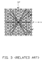
- the ground traces of the ground layer/layer are typically formed and arranged in a fashion, e.g. an array of same-sized equilateral hexagons, squares, or equilateral triangles (as shown in Figs. 1-3 ).
- the ground layer defines an X-axis along which a straight line segment of a signal trace is arranged.
- each straight line segment of a signal trace is arranged on the signal plane at an angle of 0, 30,45, 60, 90, -30, -45 or -60 degrees relative to an X-axis of the ground layer (as shown in Figs 1-3 ).
- the ground traces are also arranged at angles of 0, 30, 45, 60, 90, -30, 45 or -60 degrees relative to the X-axis of the ground layer.
- some line segments of a signal trace will cross ground traces of the ground layer at an angle causing only slight variation in impedance of the signal trace.
- some portion or portions of a signal trace line segment will be overlap with straight linear portion of a ground trace or traces of the ground layer, causing the impedance of that portion or portions of the signal trace line segment to be greatly reduced.
- the impedance of the signal trace will vary unevenly to effect signal quality.
- a circuit board for improving signal quality, including a signal layer and a ground layer.
- the signal layer includes a plurality of signal traces arranged thereon for transmitting signals therethrough.
- Each of the signal traces includes a plurality of straight line signal trace segments.
- the ground layer includes a ground trace network for being grounded.
- the ground trace network includes a plurality of linear ground trace segments.
- the linear ground trace segments cooperatively form a plurality of closed grounding loops. A projection of each of the straight line signal trace segments on the ground layer intersect a plurality of the grounding loops and does not overlap any of the linear ground trace segments of the intersected grounding loops, thereby minimizing interaction between the linear ground traces and the signal traces.
- FIG 1 is a top view of a first embodiment of a conventional ground layer of a circuit board, with straight line segments of signal traces mapped thereon;
- FIG. 2 is a top view of a second embodiment of a conventional ground layer of a circuit board, with straight lines segment of signal traces mapped thereon;
- FIG 3 is a top view of a third embodiment of a conventional ground layer of a circuit board, with straight line segments of signal traces mapped thereon;
- FIG. 4 is a cut-away view of a circuit board in accordance with a preferred embodiment, including a signal layer with a plurality of signal traces arranged thereon, a ground layer, and a media layer disposed therebetween;
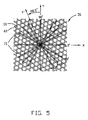
- FIG. 5 is a top view of a first embodiment of a ground layer of a circuit board in accordance with a preferred embodiment, with straight line segments of signal traces mapped thereon;
- FIG 6 is a top view of a second embodiment of a ground layer of a circuit board in accordance with a preferred embodiment, with straight line segments of signal traces mapped thereon;
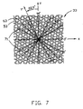
- FIG. 7 is a top view of a third embodiment of a ground layer of a circuit board in accordance with a preferred embodiment, with straight line segments of signal traces mapped thereon;
- FIG. 8 is a top view of a fourth embodiment of a ground layer of a circuit board in accordance with a preferred embodiment, with straight line segments of signal traces mapped thereon;
- FIG. 9 is a top view of a fifth embodiment of a ground layer of a circuit board in accordance with a preferred embodiment, with straight line segments of signal traces mapped thereon;
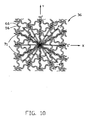
- FIG. 10 is a top view of a sixth embodiment of a ground layer of a circuit board in accordance with a preferred embodiment, with straight line segments of signal traces mapped thereon.
- the circuit board in accordance with a preferred embodiment includes a signal layer 1 with a plurality of signal traces 7 arranged thereon and a ground layer 3 for a plurality of ground traces arranged thereon.
- Each signal trace 7 includes a plurality of straight line segments.
- a media layer 2 is disposed between the signal layer 1 and the ground layer 3.
- the media layer 2 may be a dielectric layer.
- the ground layer 31 includes a ground trace network formed by a plurality of closed grounding loops 51 for being grounded.
- Each grounding loop 51 is a polygon delimited by six equal linear ground traces 61 connected consecutively end-to-end, forming an equilateral hexagon-shaped loop 51.
- the ground layer 31 defines an X-axis along which a straight line signal trace segment 71 of a signal trace 7 is arranged.
- a Y-axis of the ground layer 31 is perpendicular to the X-axis.
- a straight line passing through one linear ground trace 61 of each grounding loop 51 is designated as a Y'-axis of the grounding loop 51.
- each grounding loop 51 is rotated 22.5 degrees relative to the Y-axis of the ground layer 31.
- the ground traces 61 are oriented on the ground layer 31 at angles of 22.5, 525, 67.5, 112.5, -7.5, -22.5, or -37.5 degrees relative to the X-axis of the ground layer 31.
- Each straight line signal trace segment 71 of the signal traces 7 is arranged on the signal layer 1 at an angle of 0, 30, 45, 60, 90, -30, -45 or -60 degrees relative to the X-axis of the ground layer 31.
- each straight line signal trace segment 71 of the signal trace 7 mapped on the ground layer 31 are at an angle of at least 7.5 degrees relative to any given ground trace 61 they cross. That is, a projection of each of the straight line signal trace segments 71 on the ground layer 31 intersects the ground loops 51.
- the ground traces 61 on the ground layer 31 may be oriented at other angles relative to the ground layer 31 to ensure segments of the signal traces 7 are not coincident with the ground traces 61.
- each grounding loop 52 of the present embodiment is a polygon delimited by four equal linear ground traces 62 connected consecutively end-to-end, forming a closed square grounding loop.
- a Y'-axis of each grounding loop 52 is defined by a straight line passing through one linear ground trace 62 of the square grounding loops. The Y'-axis of are rotated 22.5 degrees relative to the Y-axis of the ground layer 32.
- each grounding loop 53 of the present embodiment is a polygon delimited by three equal linear ground traces 63 connected consecutively end-to-end, forming a triangle-shaped grounding loop.
- a Y'-axis of each grounding loop 53 is defined by a straight line passing through one linear ground trace 63 of the triangle-shaped grounding loops 53. The Y'-axis are rotated 22.5 degrees relative to the Y-axis of the ground layer 33.
- grounding loops of the ground layer could be other polygonal shapes formed by ground traces which are oriented on the ground layer at angles to ensure segments of the signal traces are not coincident with the ground traces.
- the ground layer 34 includes a plurality of same-sized grounding loops 54 with six rounded convex corners and rounded concave sides.
- Each grounding loop 54 is formed by curved ground traces 64.
- the ground layer 35 includes a plurality of same-sized grounding loops 55 with four wavy sides. Each grounding loop 55 is formed by curved ground traces 65.
- the ground layer 36 includes a plurality of same-sized grounding loops 56 with three wavy sides. Each grounding loop 56 is formed by curve ground traces 66.
- grounding loops of the ground layer may be formed as other shapes by curved ground traces.
Landscapes
- Engineering & Computer Science (AREA)
- Microelectronics & Electronic Packaging (AREA)
- Structure Of Printed Boards (AREA)
Abstract
Description
- The present invention relates to a circuit board, particularly to a circuit board with an improved ground layer.
- Circuit boards such as printed circuit boards (PCBs) are widely used in conventional electronic devices. In designing a contemporary PCB, controlling trace impedance is very important. The impedance relates to a number of parameters, such as the widths and distances of signal traces, and the thicknesses of media/insulating layers of the PCB. For example, a circuit board includes a signal plane/layer with signal traces arranged thereon and a ground layer/layer with ground traces arranged thereon. A media layer is disposed between the signal plane and the ground layer. Generally, the thickness of the media layer is so thin, that the impedance of the signal traces is reduced too much. That may affect the signal quality of the circuit board.
- Conventionally, in order to achieve a desired signal impedance of the circuit board, the ground traces of the ground layer/layer are typically formed and arranged in a fashion, e.g. an array of same-sized equilateral hexagons, squares, or equilateral triangles (as shown in
Figs. 1-3 ). The ground layer defines an X-axis along which a straight line segment of a signal trace is arranged. Generally, each straight line segment of a signal trace is arranged on the signal plane at an angle of 0, 30,45, 60, 90, -30, -45 or -60 degrees relative to an X-axis of the ground layer (as shown inFigs 1-3 ). The ground traces are also arranged at angles of 0, 30, 45, 60, 90, -30, 45 or -60 degrees relative to the X-axis of the ground layer. In designing a PCB using the preceding arrangement, some line segments of a signal trace will cross ground traces of the ground layer at an angle causing only slight variation in impedance of the signal trace. However, to the detriment of signal trace performance, some portion or portions of a signal trace line segment will be overlap with straight linear portion of a ground trace or traces of the ground layer, causing the impedance of that portion or portions of the signal trace line segment to be greatly reduced. Thus, the impedance of the signal trace will vary unevenly to effect signal quality. - What is needed, therefore, is a circuit board having proper signal trace impedance for improving signal quality.
- A circuit board is provided for improving signal quality, including a signal layer and a ground layer. The signal layer includes a plurality of signal traces arranged thereon for transmitting signals therethrough. Each of the signal traces includes a plurality of straight line signal trace segments. The ground layer includes a ground trace network for being grounded. The ground trace network includes a plurality of linear ground trace segments. The linear ground trace segments cooperatively form a plurality of closed grounding loops. A projection of each of the straight line signal trace segments on the ground layer intersect a plurality of the grounding loops and does not overlap any of the linear ground trace segments of the intersected grounding loops, thereby minimizing interaction between the linear ground traces and the signal traces.
- Other advantages and novel features of the present invention will become more apparent from the following detailed description of preferred embodiment when taken in conjunction with the accompanying drawings, in which:
-
FIG 1 is a top view of a first embodiment of a conventional ground layer of a circuit board, with straight line segments of signal traces mapped thereon; -
FIG. 2 is a top view of a second embodiment of a conventional ground layer of a circuit board, with straight lines segment of signal traces mapped thereon; -
FIG 3 is a top view of a third embodiment of a conventional ground layer of a circuit board, with straight line segments of signal traces mapped thereon; -
FIG. 4 is a cut-away view of a circuit board in accordance with a preferred embodiment, including a signal layer with a plurality of signal traces arranged thereon, a ground layer, and a media layer disposed therebetween; -
FIG. 5 is a top view of a first embodiment of a ground layer of a circuit board in accordance with a preferred embodiment, with straight line segments of signal traces mapped thereon; -
FIG 6 is a top view of a second embodiment of a ground layer of a circuit board in accordance with a preferred embodiment, with straight line segments of signal traces mapped thereon; -
FIG. 7 is a top view of a third embodiment of a ground layer of a circuit board in accordance with a preferred embodiment, with straight line segments of signal traces mapped thereon; -
FIG. 8 is a top view of a fourth embodiment of a ground layer of a circuit board in accordance with a preferred embodiment, with straight line segments of signal traces mapped thereon; -
FIG. 9 is a top view of a fifth embodiment of a ground layer of a circuit board in accordance with a preferred embodiment, with straight line segments of signal traces mapped thereon; and -
FIG. 10 is a top view of a sixth embodiment of a ground layer of a circuit board in accordance with a preferred embodiment, with straight line segments of signal traces mapped thereon. - Referring to
FIG 4 , which shows a circuit board with a ground layer for improving the signal quality, the circuit board in accordance with a preferred embodiment includes asignal layer 1 with a plurality ofsignal traces 7 arranged thereon and aground layer 3 for a plurality of ground traces arranged thereon. Eachsignal trace 7 includes a plurality of straight line segments. Amedia layer 2 is disposed between thesignal layer 1 and theground layer 3. Themedia layer 2 may be a dielectric layer. - Referring to
FIG 5 , aground layer 31 in accordance with a first embodiment of the present invention is shown. Theground layer 31 includes a ground trace network formed by a plurality of closedgrounding loops 51 for being grounded. Eachgrounding loop 51 is a polygon delimited by six equal linear ground traces 61 connected consecutively end-to-end, forming an equilateral hexagon-shaped loop 51. Theground layer 31 defines an X-axis along which a straight linesignal trace segment 71 of asignal trace 7 is arranged. A Y-axis of theground layer 31 is perpendicular to the X-axis. A straight line passing through one linear ground trace 61 of eachgrounding loop 51 is designated as a Y'-axis of thegrounding loop 51. In the present embodiment, the Y'-axis of eachgrounding loop 51 is rotated 22.5 degrees relative to the Y-axis of theground layer 31. Thus, the ground traces 61 are oriented on theground layer 31 at angles of 22.5, 525, 67.5, 112.5, -7.5, -22.5, or -37.5 degrees relative to the X-axis of theground layer 31. Each straight linesignal trace segment 71 of thesignal traces 7 is arranged on thesignal layer 1 at an angle of 0, 30, 45, 60, 90, -30, -45 or -60 degrees relative to the X-axis of theground layer 31. Thus, different portions of each straight linesignal trace segment 71 of thesignal trace 7 mapped on theground layer 31 are at an angle of at least 7.5 degrees relative to any given ground trace 61 they cross. That is, a projection of each of the straight linesignal trace segments 71 on theground layer 31 intersects theground loops 51. With this arrangement interaction between the ground traces and the signal traces is minimized to reduce differences in impedances of the signal traces and cause the impedance of segments of the signal traces to vary evenly, thereby greatly improving signal quality. Wherein the ground traces 61 on theground layer 31 may be oriented at other angles relative to theground layer 31 to ensure segments of thesignal traces 7 are not coincident with the ground traces 61. - Referring to
Fig. 6 , aground layer 32 of a circuit board in accordance with a second embodiment is shown. Theground layer 32 of the second embodiment is similar to that ofFig.5 , but eachgrounding loop 52 of the present embodiment is a polygon delimited by four equallinear ground traces 62 connected consecutively end-to-end, forming a closed square grounding loop. A Y'-axis of eachgrounding loop 52 is defined by a straight line passing through onelinear ground trace 62 of the square grounding loops. The Y'-axis of are rotated 22.5 degrees relative to the Y-axis of theground layer 32. - Referring to
Fig. 7 , aground layer 33 of a circuit board in accordance with a third embodiment is shown. Theground layer 33 of the third embodiment is similar to that ofFig.5 , but eachgrounding loop 53 of the present embodiment is a polygon delimited by three equallinear ground traces 63 connected consecutively end-to-end, forming a triangle-shaped grounding loop. A Y'-axis of eachgrounding loop 53 is defined by a straight line passing through onelinear ground trace 63 of the triangle-shaped grounding loops 53. The Y'-axis are rotated 22.5 degrees relative to the Y-axis of theground layer 33. - Wherein the grounding loops of the ground layer could be other polygonal shapes formed by ground traces which are oriented on the ground layer at angles to ensure segments of the signal traces are not coincident with the ground traces.
- Referring to
FIG. 8 , aground layer 34 of a circuit board in accordance with a fourth embodiment is shown. In this embodiment, theground layer 34 includes a plurality of same-sized grounding loops 54 with six rounded convex corners and rounded concave sides. Eachgrounding loop 54 is formed bycurved ground traces 64. - Referring to
FIG. 9 , aground layer 35 of a circuit board in accordance with a fifth embodiment is shown. In this embodiment, theground layer 35 includes a plurality of same-sized grounding loops 55 with four wavy sides. Each grounding loop 55 is formed by curved ground traces 65. - Referring to
FIG. 10 , aground layer 36 of a circuit board in accordance with a sixth embodiment is shown. In this embodiment, theground layer 36 includes a plurality of same-sized grounding loops 56 with three wavy sides. Each grounding loop 56 is formed by curve ground traces 66. - According to the above, different portions of each line segment of a signal trace mapped on the ground layer will cross any given ground trace at a similar angle since the grounding loops are formed by curved ground traces. With this arrangement, interaction between the ground traces and the signal traces is minimized to reduce differences in impedances of the signal traces and cause the impedance of segments of the signal traces to vary evenly, thereby greatly improving signal quality. Wherein the grounding loops of the ground layer may be formed as other shapes by curved ground traces.
- It is to be understood, however, that even through numerous characteristics and advantages of the present invention have been set forth in the foregoing description, together with details of the structure and function of the invention, the disclosure is illustrative only, and changes may be made in detail, especially in matters of shape, size, and arrangement of parts within the principles of the invention to the full extent indicated by the broad general meaning of the terms in which the appended claims are expressed.
Claims (15)
- A circuit board comprising:a media layer having a first surface and an opposite second surface;a signal layer formed on the first surface, the signal layer comprising a plurality of signal traces arranged thereon for transmitting signals therethrough, each of the signal traces comprising a plurality of straight line signal trace segments; anda ground layer formed on the second surface, the ground layer comprising a ground trace network for being grounded, the ground trace network comprising a plurality of linear ground trace segments which cooperatively form a plurality of closed grounding loops, a projection of each of the straight line signal trace segments on the ground layer intersecting a plurality of the grounding loops and not overlapping any of the linear ground trace segments of the intersected grounding loops, thereby minimizing interaction between the linear ground traces and the signal traces.
- A circuit board as claimed in claim 1, wherein each of the grounding loops is a polygon in shape.
- A circuit board as claimed in claim 1 or 2, wherein each of the grounding loops is an equilateral polygon in shape.
- A circuit board as claimed in claim 1, 2 or 3, wherein the projection of each of the straight line signal trace segments on the ground layer obliquely intersects the intersected linear ground trace segments of the intersected grounding loops at an angle of at least about 75 degrees.
- A circuit board as claimed in any preceding claim, wherein a main plane of the ground layer defines an X-axis along which some of the straight line signal trace segments of one of the signal traces are oriented and a Y-axis perpendicular to the X-axis, the projection of the straight line signal trace segments of each signal trace on the ground layer being at angles of 0, 30, 45, 60, 90, -30, -45, or -60 degrees relative to the X-axis, a Y'-axis being defined by a straight line passing through one ground trace segment of one loop, wherein the Y'-axis is inclined relative to the Y-axis at 22.5 degrees.
- A circuit board as claimed in claim 1, wherein the grounding loops form a regular repeated pattern.
- A circuit board as claimed in claim 1, wherein the projection of each of the straight line signal trace segments on the ground layer is not parallel to any of the linear ground trace segments of the intersected grounding loops
- A circuit board comprising:a ground layer;a media plane layered over the ground layer; anda signal plane layered over the media plane, the signal plane having a plurality of signal traces arranged thereon, each of the signal traces comprising a plurality of straight line signal trace segments; whereinthe ground layer comprises a network having a plurality of loops connected to each other in a regular repeated pattern, the network comprising a plurality of ground traces which cooperatively form the loops, a projection of each of straight line segments on the ground layer intersecting some of the loops, the ground traces of the intersected loops being curved.
- A circuit board as claimed in claim 8, wherein each of the loops is a polygon in shape.
- A circuit board comprising:a media layer having a first surface and an opposite second surface;a signal layer formed on the first surface, the signal layer comprising a signal trace arranged thereon for transmitting signals therethrough, the signal trace comprising a plurality of straight line signal trace segments; anda ground layer formed on the second surface, the ground layer comprising a ground trace network for being grounded, the ground trace network comprising a plurality of curved ground traces which cooperatively form a plurality of closed grounding loops.
- A circuit board as claimed in claim 10, wherein the curved ground traces consists of a plurality of curved ridges and troughs.
- A circuit board as claimed in claim 10 or 11, wherein the loops have a common shape.
- A circuit board as claimed in any of claim 10 to 12, wherein the shape of each of the loops is substantially identical to a loop shown in FIG. 8.
- A circuit board as claimed in any of claims 10 to 12, wherein the shape of each of the loops is substantially identical to a loop shown in FIG. 9.
- A circuit board as claimed in any of claims 10 to 12, wherein the shape of each of the loops is substantially identical to a loop shown in FIG. 10.
Priority Applications (1)
| Application Number | Priority Date | Filing Date | Title |
|---|---|---|---|
| EP08251484.5A EP2112871B1 (en) | 2008-04-22 | 2008-04-22 | Circuit board with improved ground layer |
Applications Claiming Priority (1)
| Application Number | Priority Date | Filing Date | Title |
|---|---|---|---|
| EP08251484.5A EP2112871B1 (en) | 2008-04-22 | 2008-04-22 | Circuit board with improved ground layer |
Publications (2)
| Publication Number | Publication Date |
|---|---|
| EP2112871A1 true EP2112871A1 (en) | 2009-10-28 |
| EP2112871B1 EP2112871B1 (en) | 2016-07-13 |
Family
ID=39745123
Family Applications (1)
| Application Number | Title | Priority Date | Filing Date |
|---|---|---|---|
| EP08251484.5A Not-in-force EP2112871B1 (en) | 2008-04-22 | 2008-04-22 | Circuit board with improved ground layer |
Country Status (1)
| Country | Link |
|---|---|
| EP (1) | EP2112871B1 (en) |
Citations (6)
| Publication number | Priority date | Publication date | Assignee | Title |
|---|---|---|---|---|
| US5360949A (en) | 1993-06-30 | 1994-11-01 | Northern Telecom Limited | Printed circuit board |
| JPH06326476A (en) | 1993-05-13 | 1994-11-25 | Sony Corp | Multilayer wiring board |
| US20060144616A1 (en) * | 2004-12-30 | 2006-07-06 | Hon Hai Precision Industry Co., Ltd. | Printed circuit board with improved ground plane |
| EP1720384A2 (en) * | 2005-04-28 | 2006-11-08 | Nitto Denko Corporation | Printed circuit board |
| WO2007099596A1 (en) | 2006-02-28 | 2007-09-07 | Sony Chemical & Information Device Corporation | Wiring board, method for arranging wiring pattern |
| US20080151521A1 (en) * | 2006-12-22 | 2008-06-26 | Hon Hai Precision Industry Co., Ltd. | Circuit board with improved ground plane |
-
2008
- 2008-04-22 EP EP08251484.5A patent/EP2112871B1/en not_active Not-in-force
Patent Citations (6)
| Publication number | Priority date | Publication date | Assignee | Title |
|---|---|---|---|---|
| JPH06326476A (en) | 1993-05-13 | 1994-11-25 | Sony Corp | Multilayer wiring board |
| US5360949A (en) | 1993-06-30 | 1994-11-01 | Northern Telecom Limited | Printed circuit board |
| US20060144616A1 (en) * | 2004-12-30 | 2006-07-06 | Hon Hai Precision Industry Co., Ltd. | Printed circuit board with improved ground plane |
| EP1720384A2 (en) * | 2005-04-28 | 2006-11-08 | Nitto Denko Corporation | Printed circuit board |
| WO2007099596A1 (en) | 2006-02-28 | 2007-09-07 | Sony Chemical & Information Device Corporation | Wiring board, method for arranging wiring pattern |
| US20080151521A1 (en) * | 2006-12-22 | 2008-06-26 | Hon Hai Precision Industry Co., Ltd. | Circuit board with improved ground plane |
Also Published As
| Publication number | Publication date |
|---|---|
| EP2112871B1 (en) | 2016-07-13 |
Similar Documents
| Publication | Publication Date | Title |
|---|---|---|
| US7663063B2 (en) | Circuit board with improved ground plane | |
| JP5424417B2 (en) | Printed circuit board | |
| JP5999239B2 (en) | Signal transmission parts and electronic equipment | |
| US20080144295A1 (en) | Flexible printed circuit board | |
| CN1119903A (en) | A circuit board device containing shielding net and its structure | |
| US8420946B2 (en) | Printed circuit board | |
| US8648668B2 (en) | Electrical impedance precision control of signal transmission line for circuit board | |
| WO2010103721A1 (en) | Circuit board | |
| US7973244B2 (en) | Printed circuit board | |
| US8256111B2 (en) | Circuit board layout method | |
| US9590288B2 (en) | Multilayer circuit substrate | |
| US8071885B2 (en) | Printed circuit board | |
| CN105611718B (en) | Flexible circuit board | |
| JP6097088B2 (en) | Printed wiring board and conductor sheet for printed wiring board | |
| US20060144616A1 (en) | Printed circuit board with improved ground plane | |
| US20060255878A1 (en) | Printed wiring board | |
| US8502617B2 (en) | Printed circuit board | |
| US20090071702A1 (en) | Circuit board | |
| EP2112871B1 (en) | Circuit board with improved ground layer | |
| US20110205715A1 (en) | Transmission line circuit having pairs of crossing conductive lines | |
| US10757800B1 (en) | Stripline transmission lines with cross-hatched pattern return plane, where the striplines do not overlap any intersections in the cross-hatched pattern | |
| TWI665945B (en) | Radio frequency printed circuit board and method for manufacturing the same | |
| CN1615067A (en) | Differential wire assembling method for eliminating high speed board interferes | |
| JP4596955B2 (en) | Wiring board | |
| CN117855852A (en) | Metamaterial structure and antenna housing |
Legal Events
| Date | Code | Title | Description |
|---|---|---|---|
| PUAI | Public reference made under article 153(3) epc to a published international application that has entered the european phase |
Free format text: ORIGINAL CODE: 0009012 |
|
| AK | Designated contracting states |
Kind code of ref document: A1 Designated state(s): AT BE BG CH CY CZ DE DK EE ES FI FR GB GR HR HU IE IS IT LI LT LU LV MC MT NL NO PL PT RO SE SI SK TR |
|
| AX | Request for extension of the european patent |
Extension state: AL BA MK RS |
|
| 17P | Request for examination filed |
Effective date: 20100119 |
|
| 17Q | First examination report despatched |
Effective date: 20100312 |
|
| AKX | Designation fees paid |
Designated state(s): DE FR GB |
|
| GRAP | Despatch of communication of intention to grant a patent |
Free format text: ORIGINAL CODE: EPIDOSNIGR1 |
|
| GRAS | Grant fee paid |
Free format text: ORIGINAL CODE: EPIDOSNIGR3 |
|
| INTG | Intention to grant announced |
Effective date: 20160512 |
|
| GRAA | (expected) grant |
Free format text: ORIGINAL CODE: 0009210 |
|
| AK | Designated contracting states |
Kind code of ref document: B1 Designated state(s): DE FR GB |
|
| REG | Reference to a national code |
Ref country code: GB Ref legal event code: FG4D |
|
| REG | Reference to a national code |
Ref country code: DE Ref legal event code: R096 Ref document number: 602008045060 Country of ref document: DE |
|
| REG | Reference to a national code |
Ref country code: DE Ref legal event code: R097 Ref document number: 602008045060 Country of ref document: DE |
|
| PLBE | No opposition filed within time limit |
Free format text: ORIGINAL CODE: 0009261 |
|
| STAA | Information on the status of an ep patent application or granted ep patent |
Free format text: STATUS: NO OPPOSITION FILED WITHIN TIME LIMIT |
|
| 26N | No opposition filed |
Effective date: 20170418 |
|
| REG | Reference to a national code |
Ref country code: DE Ref legal event code: R119 Ref document number: 602008045060 Country of ref document: DE |
|
| GBPC | Gb: european patent ceased through non-payment of renewal fee |
Effective date: 20170422 |
|
| REG | Reference to a national code |
Ref country code: FR Ref legal event code: ST Effective date: 20171229 |
|
| PG25 | Lapsed in a contracting state [announced via postgrant information from national office to epo] |
Ref country code: DE Free format text: LAPSE BECAUSE OF NON-PAYMENT OF DUE FEES Effective date: 20171103 Ref country code: FR Free format text: LAPSE BECAUSE OF NON-PAYMENT OF DUE FEES Effective date: 20170502 |
|
| PG25 | Lapsed in a contracting state [announced via postgrant information from national office to epo] |
Ref country code: GB Free format text: LAPSE BECAUSE OF NON-PAYMENT OF DUE FEES Effective date: 20170422 |