EP2109144A1 - Organic light emitting diode display and method of manufacturing the same - Google Patents
Organic light emitting diode display and method of manufacturing the same Download PDFInfo
- Publication number
- EP2109144A1 EP2109144A1 EP09154966A EP09154966A EP2109144A1 EP 2109144 A1 EP2109144 A1 EP 2109144A1 EP 09154966 A EP09154966 A EP 09154966A EP 09154966 A EP09154966 A EP 09154966A EP 2109144 A1 EP2109144 A1 EP 2109144A1
- Authority
- EP
- European Patent Office
- Prior art keywords
- bezel
- display
- display panel
- oled display
- oled
- Prior art date
- Legal status (The legal status is an assumption and is not a legal conclusion. Google has not performed a legal analysis and makes no representation as to the accuracy of the status listed.)
- Granted
Links
Images


Classifications
-
- H—ELECTRICITY
- H10—SEMICONDUCTOR DEVICES; ELECTRIC SOLID-STATE DEVICES NOT OTHERWISE PROVIDED FOR
- H10K—ORGANIC ELECTRIC SOLID-STATE DEVICES
- H10K59/00—Integrated devices, or assemblies of multiple devices, comprising at least one organic light-emitting element covered by group H10K50/00
- H10K59/80—Constructional details
- H10K59/87—Passivation; Containers; Encapsulations
-
- B—PERFORMING OPERATIONS; TRANSPORTING
- B21—MECHANICAL METAL-WORKING WITHOUT ESSENTIALLY REMOVING MATERIAL; PUNCHING METAL
- B21B—ROLLING OF METAL
- B21B1/00—Metal-rolling methods or mills for making semi-finished products of solid or profiled cross-section; Sequence of operations in milling trains; Layout of rolling-mill plant, e.g. grouping of stands; Succession of passes or of sectional pass alternations
- B21B1/22—Metal-rolling methods or mills for making semi-finished products of solid or profiled cross-section; Sequence of operations in milling trains; Layout of rolling-mill plant, e.g. grouping of stands; Succession of passes or of sectional pass alternations for rolling plates, strips, bands or sheets of indefinite length
- B21B1/24—Metal-rolling methods or mills for making semi-finished products of solid or profiled cross-section; Sequence of operations in milling trains; Layout of rolling-mill plant, e.g. grouping of stands; Succession of passes or of sectional pass alternations for rolling plates, strips, bands or sheets of indefinite length in a continuous or semi-continuous process
- B21B1/28—Metal-rolling methods or mills for making semi-finished products of solid or profiled cross-section; Sequence of operations in milling trains; Layout of rolling-mill plant, e.g. grouping of stands; Succession of passes or of sectional pass alternations for rolling plates, strips, bands or sheets of indefinite length in a continuous or semi-continuous process by cold-rolling, e.g. Steckel cold mill
-
- B—PERFORMING OPERATIONS; TRANSPORTING
- B21—MECHANICAL METAL-WORKING WITHOUT ESSENTIALLY REMOVING MATERIAL; PUNCHING METAL
- B21B—ROLLING OF METAL
- B21B1/00—Metal-rolling methods or mills for making semi-finished products of solid or profiled cross-section; Sequence of operations in milling trains; Layout of rolling-mill plant, e.g. grouping of stands; Succession of passes or of sectional pass alternations
- B21B1/22—Metal-rolling methods or mills for making semi-finished products of solid or profiled cross-section; Sequence of operations in milling trains; Layout of rolling-mill plant, e.g. grouping of stands; Succession of passes or of sectional pass alternations for rolling plates, strips, bands or sheets of indefinite length
- B21B1/30—Metal-rolling methods or mills for making semi-finished products of solid or profiled cross-section; Sequence of operations in milling trains; Layout of rolling-mill plant, e.g. grouping of stands; Succession of passes or of sectional pass alternations for rolling plates, strips, bands or sheets of indefinite length in a non-continuous process
- B21B1/32—Metal-rolling methods or mills for making semi-finished products of solid or profiled cross-section; Sequence of operations in milling trains; Layout of rolling-mill plant, e.g. grouping of stands; Succession of passes or of sectional pass alternations for rolling plates, strips, bands or sheets of indefinite length in a non-continuous process in reversing single stand mills, e.g. with intermediate storage reels for accumulating work
- B21B1/36—Metal-rolling methods or mills for making semi-finished products of solid or profiled cross-section; Sequence of operations in milling trains; Layout of rolling-mill plant, e.g. grouping of stands; Succession of passes or of sectional pass alternations for rolling plates, strips, bands or sheets of indefinite length in a non-continuous process in reversing single stand mills, e.g. with intermediate storage reels for accumulating work by cold-rolling
-
- G—PHYSICS
- G02—OPTICS
- G02F—OPTICAL DEVICES OR ARRANGEMENTS FOR THE CONTROL OF LIGHT BY MODIFICATION OF THE OPTICAL PROPERTIES OF THE MEDIA OF THE ELEMENTS INVOLVED THEREIN; NON-LINEAR OPTICS; FREQUENCY-CHANGING OF LIGHT; OPTICAL LOGIC ELEMENTS; OPTICAL ANALOGUE/DIGITAL CONVERTERS
- G02F1/00—Devices or arrangements for the control of the intensity, colour, phase, polarisation or direction of light arriving from an independent light source, e.g. switching, gating or modulating; Non-linear optics
- G02F1/01—Devices or arrangements for the control of the intensity, colour, phase, polarisation or direction of light arriving from an independent light source, e.g. switching, gating or modulating; Non-linear optics for the control of the intensity, phase, polarisation or colour
- G02F1/13—Devices or arrangements for the control of the intensity, colour, phase, polarisation or direction of light arriving from an independent light source, e.g. switching, gating or modulating; Non-linear optics for the control of the intensity, phase, polarisation or colour based on liquid crystals, e.g. single liquid crystal display cells
- G02F1/133—Constructional arrangements; Operation of liquid crystal cells; Circuit arrangements
- G02F1/1333—Constructional arrangements; Manufacturing methods
- G02F1/133308—Support structures for LCD panels, e.g. frames or bezels
- G02F1/133314—Back frames
-
- G—PHYSICS
- G02—OPTICS
- G02F—OPTICAL DEVICES OR ARRANGEMENTS FOR THE CONTROL OF LIGHT BY MODIFICATION OF THE OPTICAL PROPERTIES OF THE MEDIA OF THE ELEMENTS INVOLVED THEREIN; NON-LINEAR OPTICS; FREQUENCY-CHANGING OF LIGHT; OPTICAL LOGIC ELEMENTS; OPTICAL ANALOGUE/DIGITAL CONVERTERS
- G02F1/00—Devices or arrangements for the control of the intensity, colour, phase, polarisation or direction of light arriving from an independent light source, e.g. switching, gating or modulating; Non-linear optics
- G02F1/01—Devices or arrangements for the control of the intensity, colour, phase, polarisation or direction of light arriving from an independent light source, e.g. switching, gating or modulating; Non-linear optics for the control of the intensity, phase, polarisation or colour
- G02F1/13—Devices or arrangements for the control of the intensity, colour, phase, polarisation or direction of light arriving from an independent light source, e.g. switching, gating or modulating; Non-linear optics for the control of the intensity, phase, polarisation or colour based on liquid crystals, e.g. single liquid crystal display cells
- G02F1/133—Constructional arrangements; Operation of liquid crystal cells; Circuit arrangements
- G02F1/1333—Constructional arrangements; Manufacturing methods
- G02F1/133308—Support structures for LCD panels, e.g. frames or bezels
- G02F1/133328—Segmented frames
-
- H—ELECTRICITY
- H10—SEMICONDUCTOR DEVICES; ELECTRIC SOLID-STATE DEVICES NOT OTHERWISE PROVIDED FOR
- H10K—ORGANIC ELECTRIC SOLID-STATE DEVICES
- H10K50/00—Organic light-emitting devices
- H10K50/80—Constructional details
- H10K50/84—Passivation; Containers; Encapsulations
-
- G—PHYSICS
- G02—OPTICS
- G02F—OPTICAL DEVICES OR ARRANGEMENTS FOR THE CONTROL OF LIGHT BY MODIFICATION OF THE OPTICAL PROPERTIES OF THE MEDIA OF THE ELEMENTS INVOLVED THEREIN; NON-LINEAR OPTICS; FREQUENCY-CHANGING OF LIGHT; OPTICAL LOGIC ELEMENTS; OPTICAL ANALOGUE/DIGITAL CONVERTERS
- G02F1/00—Devices or arrangements for the control of the intensity, colour, phase, polarisation or direction of light arriving from an independent light source, e.g. switching, gating or modulating; Non-linear optics
- G02F1/01—Devices or arrangements for the control of the intensity, colour, phase, polarisation or direction of light arriving from an independent light source, e.g. switching, gating or modulating; Non-linear optics for the control of the intensity, phase, polarisation or colour
- G02F1/13—Devices or arrangements for the control of the intensity, colour, phase, polarisation or direction of light arriving from an independent light source, e.g. switching, gating or modulating; Non-linear optics for the control of the intensity, phase, polarisation or colour based on liquid crystals, e.g. single liquid crystal display cells
- G02F1/133—Constructional arrangements; Operation of liquid crystal cells; Circuit arrangements
- G02F1/1333—Constructional arrangements; Manufacturing methods
- G02F1/133308—Support structures for LCD panels, e.g. frames or bezels
-
- G—PHYSICS
- G02—OPTICS
- G02F—OPTICAL DEVICES OR ARRANGEMENTS FOR THE CONTROL OF LIGHT BY MODIFICATION OF THE OPTICAL PROPERTIES OF THE MEDIA OF THE ELEMENTS INVOLVED THEREIN; NON-LINEAR OPTICS; FREQUENCY-CHANGING OF LIGHT; OPTICAL LOGIC ELEMENTS; OPTICAL ANALOGUE/DIGITAL CONVERTERS
- G02F2201/00—Constructional arrangements not provided for in groups G02F1/00 - G02F7/00
- G02F2201/50—Protective arrangements
- G02F2201/503—Arrangements improving the resistance to shock
Definitions
- the present invention relates to an Organic Light Emitting Diode (OLED) display, a module for an OLED display and a method of manufacturing the same.
- OLED Organic Light Emitting Diode
- An active matrix OLED display using an organic light emitting element independently controls a pixel by arranging pixels on a substrate in a matrix method.
- the pixel is the basic unit for representing an image, and each pixel contains a thin film transistor (TFT) and an organic light emitting element.
- TFT thin film transistor
- the organic light emitting element includes a hole injection electrode, an organic emission layer, and an electron injection electrode, and light is emitted by energy that is generated when an exciton that is generated by coupling of electrons and holes falls from an exited state to a ground state within the organic emission layer. Due to such a principle, because the OLED display has self-luminance characteristics, and unlike a Liquid Crystal Display (LCD), does not require a separate light source, a thickness and a weight of the OLED is reduced. Further, because the OLED display has beneficial characteristics such as low power consumption, high luminance, and high reaction speed, the OLED display is appropriate for being used in a mobile electronic device.
- LCD Liquid Crystal Display
- the OLED display includes a display panel having two substrates that are fixed together by a sealant, a bezel that is coupled to the display panel, and a printed circuit board that is electrically connected to the display panel through a flexible printed circuit (FPC), thereby forming a module.
- a display panel having two substrates that are fixed together by a sealant
- a bezel that is coupled to the display panel
- a printed circuit board that is electrically connected to the display panel through a flexible printed circuit (FPC), thereby forming a module.
- FPC flexible printed circuit
- the present invention provides an OLED display and a method of manufacturing the same having advantages of having excellent mechanical strength characteristics.
- An exemplary embodiment of the present invention provides an OLED display including a display panel and a bezel arrangement to receive the display panel, the bezel arrangement including a first bezel and a second bezel, each of the first bezel and the second bezel including different materials and including a bottom portion and a skirt portion protruding from edges of the bottom portion.
- the first bezel and the second bezel can be integrally formed as a single integrated monolithic unit.
- the first bezel and the second bezel can be of a same shape.
- the first bezel can have a lower surface hardness and a higher elastic modulus than that of the second bezel.
- the first bezel can include or is made of a resin.
- the first bezel can be formed or made of polycarbonate (PC).
- the second bezel can be a metal.
- the second bezel can be one of stainless using steel (SUS), steel plate cold commercial (SPCC), aluminum, and a nickel-silver alloy. At least one opening can be arranged in a bottom portion of
- the OLED display can be a portable display device.
- a method of making an OLED display including mounting a first bezel within a second bezel, the first bezel being of a different material than the second bezel and arranging a display panel within the first bezel.
- an alternative method of making an OLED display including inserting a second bezel into an injection mold, injecting the first bezel with a material different from that of the second bezel to integrally form the first bezel and the second bezel and arranging the display panel within the first bezel.
- FIG. 1 is an exploded perspective view illustrating an OLED display 100 according a first an exemplary embodiment of the present invention
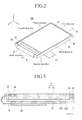
- FIG. 2 is a perspective view illustrating a state in which a display panel 10 that is shown in FIG. 1 is received in a first bezel 30 and a second bezel 32.
- the display panel is arranged on top of a bottom surface of the first bezel 30, which itself is arranged on top of a bottom surface of the second bezel 32.
- the OLED display 100 includes a display panel 10 that displays an image and the first bezel 30 and the second bezel 32 that receive the display panel 10.
- the face of the display panel 10 which displays the image is the opposite face of the display panel 10 which faces the first and second bezel 30, 32.
- the display panel 10 can be for a portable device, such as a cellular phone.
- the display panel 10 can instead be for a large sized appliance, like a television set.
- the display panel 10 includes a first substrate 12, and a second substrate 14 that has a smaller size than the first substrate 12.
- a display area DA where the image is actually displayed is located where the second substrate 14 overlaps the first substrate 12.
- the display device 100 has an active matrix (AM) structure, organic light emitting elements, thin film transistors (TFTs) for driving the organic light emitting elements, and wires that are electrically connected thereto are formed on the first substrate 12 to correspond to the display area DA.
- AM active matrix
- TFTs thin film transistors
- a pad area PA is formed on a portion of the first substrate 12 that is not overlapped by the second substrate 14, and a pad (not shown) that extends from the wires of the display area DA is positioned within the pad area PA.
- the pads are electrically connected to a printed circuit board (PCB) 20 through a flexible printed circuit (FPC) 18.
- PCB printed circuit board
- FPC flexible printed circuit
- electronic elements (not shown) for processing a driving signal are mounted and a connector (not shown) for transmitting an external signal to the PCB 20 is provided.
- An integrated circuit (IC) chip 16 is mounted in the pad area PA of the first substrate 12 to control the display panel 10.
- the integrated circuit chip 16 generates a plurality of timing signals for applying data driving signals and gate driving signals at an appropriate point of time to the data lines and the gate lines respectively of the display panel 10.
- a protective layer 22 is formed around the integrated circuit chip 16 to protect the integrated circuit chip 16.
- the FPC 18 fixed to the display panel 10 is bent to the rear side of the second bezel 32 so that the PCB 20 is positioned at a rear surface of the second bezel 32.
- the OLED display 100 of the first exemplary embodiment includes the first bezel 30 and the second bezel 32.
- the display panel 10 is arranged within the first bezel 30, and the first bezel 30 is mounted within the second bezel 32.
- the first bezel 30 includes a first bottom portion 302 corresponding to a size of the display panel 10 and a first skirt portion 304 that is arranged to be perpendicular to the first bottom portion 302 and extend a predetermined height from an edge of the first bottom portion 302.
- the first skirt portion 304 at the side in which the FPC 18 is arranged is cut out so that the FPC 18 can be positioned thereat without interference.
- the respective skirt portion 304 is provided with a stepped profile having higher parts where the FPC 18 is not arranged and lower parts where the FPC 18 is arranged.
- the first bezel 30 is arranged to be received within the second bezel 32.
- the second bezel 32 can have the same shape as that of the first bezel 30 and entirely surround the entire first bezel 30. That is, the second bezel 32 includes a second bottom portion 322 and a second skirt portion 324 corresponding to the first bottom portion 302 and the first skirt portion 304 of the first bezel 30. As with the first skirt portion 304, the second skirt portion 324 at the side in which the FPC 18 is arranged can be cut out so that the FPC 18 can be positioned thereat without interference.
- a part of the second bottom portion 322 is also cut out to form a groove portion 326 where the part of the second bottom portion 322 is recessed. Through the groove portion 326, a part of the first bezel 30 is exposed in the second bottom portion 322.
- first bezel 30 be separated from the second bezel 32 due to a failure that occurs in a process of assembling the first bezel 30 and the second bezel 32, force from the outside can be applied to the portion of the first bezel 30 that is exposed through the groove portion 326 so that the first bezel 30 can be easily separated from the second bezel 32.
- a method of manufacturing the first bezel 30 and the second bezel 32 is as follows. First, the first bezel 30 and the second bezel 32 are individually manufactured. In this case, the first bezel 30 can be manufactured so that the first bezel 30 can be mounted within the second bezel 32. For example, it is preferable that the first bezel 30 be completely inserted into the second bezel 32, and after the first bezel 30 is mounted within the second bezel 32, the first bezel 30 is manufactured to have a size so that it is not easily separated from the second bezel 32. When assembly of the first bezel 30 and the second bezel 32 is completed, the display panel 10 is fitted within the first bezel 30.
- the first bezel 30 and the second bezel 32 can be integrally formed.
- the second bezel 32 is inserted within an injection mold, and the first bezel 30 is injected so that it is formed within the second bezel 32.
- Injection molding can be easily understood by those skilled in the art and therefore a detailed description thereof is omitted.
- first bezel 30 and the second bezel 32 are manufactured via injection molding, because both the first bezel 30 and the second bezel 32 can be simultaneously formed, an assembly process of the first bezel 30 and the second bezel 32 can be omitted. Further, because the first bezel 30 and the second bezel 32 are integrally formed, there is an advantage that the first bezel 30 can not be separated from the second bezel 32.
- the first bezel 30 and the second bezel 32 can have different strengths. Because the first bezel 30 contacts the rear surface 121 of the display panel 10 whose substrate is generally made out of glass, the first bezel 30 preferably has a relatively low strength so that the display panel 10 is not easily broken by impact.
- the first bezel 30 can be made out of a resin.
- the first bezel 30 can be made out of an engineering plastic, particularly polycarbonate (PC).
- PC polycarbonate
- engineering plastics have excellent heat resistance, mechanical strength, wear resistance, and insulation
- engineering plastics are widely used in a mechanical part of an electronic device.
- PC has high mechanical strength (bending strength), excellent heat resistance, electric insulation, and a most excellent impact strength among thermoplastic resins. Further, PC has very stable physical characteristics, even with an environmental change, such as a change of humidity and temperature.
- PC has a tension strength of 650kg/cm 2 , a bending strength of 900kg/cm 2 , an elastic modulus of 2800MPa, and a density of 1.2 ⁇ 10 -9 Ton/mm 3 .
- PC is about 1/100 times greater in an elastic modulus than stainless steel (SUS) (206000MPa) and about 1 ⁇ 2 times greater in density than a glass substrate (2.5 ⁇ 10 -9 Ton/mm 3 ) used in a display panel.
- the first bezel 30 can sufficiently protect the display panel 10. Further, because PC is 100 times greater in an elastic modulus than SUS, PC can be stable during bending while absorbing an external impact, compared to when the display panel 10 is received in an SUS bezel.
- the second bezel 32 can be made out of a material having a relatively high strength in order to sufficiently protect the display panel 10.
- the second bezel 32 can be made out of a metal material such as SUS, Cold Rolled Carbon Steel Sheets and Strip (SPCC), aluminum, or a nickel-silver alloy having predetermined strength.
- a material for the second bezel 32 is not limited to the above-described material.
- the display panel 10 when the first bezel 30 that is made out of a resin material and the second bezel 32 that is made out of a metal material are used together, by advancing strength through the second bezel 32 while effectively protecting the display panel 10 from an external impact through a shock-absorbing effect of the first bezel 30, when a falling or static load is applied to the OLED display 100, the display panel 10 can be prevented from being damaged.
- FIG. 3 is a cross-sectional view of the OLED display taken along line III-III of FIG. 2 .
- the display panel 10 is received within the first bezel 30, and the second bezel 32 supports the display panel 10 and the first bezel 30 while surrounding the first bezel 30.
- the first bezel 30 is inserted between the display panel 10 and the second bezel 32, and a rear surface 121 of the display panel 10 and the first bottom portion 302 of the first bezel 30 contact each other.
- the first bezel 30 can perform a shock-absorbing function for the display panel 10
- the second bezel 32 performs a function of supporting the display panel 10, so that the mechanical strength of the OLED display 100 can be reinforced.
- the OLED display 100 of the first exemplary embodiment can further include a shock-absorbing tape (not shown), such as a poron tape between the display panel 10 and the first bottom portion 302 of the first bezel 30.
- a shock-absorbing tape such as a poron tape between the display panel 10 and the first bottom portion 302 of the first bezel 30.
- the OLED display 100 that is formed in this way is provided within a case of a product (such as a cellular phone) to display an image that is requested by the user.
- FIG. 4 is a perspective view illustrating a bezel portion only of an OLED display according to a second exemplary embodiment of the present invention.
- this bezel includes a plurality of bezels, i.e., a first bezel 30' and a second bezel 32'.
- the first bezel 30' and the second bezel 32' can be individually manufactured and assembled or integrally formed together via injection molding, as with the first bezel 30 and the second bezel 32 of the first embodiment.
- the first bezel 30' and the second bezel 32' of the second embodiment can include a bottom portion and a skirt portion having a shape similar to that of the first bezel 30 and the second bezel 32 of the first embodiment, and a material thereof can be the same as that of the first bezel 30 and the second bezel 32 of the first embodiment.
- the first bezel 30' and the second bezel 32' have a plurality of first openings 3021' and second openings 3221', respectively in a bottom portion thereof.
- the first openings 3021' are positioned apart from each other, and the second openings 3221' are positioned to correspond to the first openings 3021'. Because the first bezel 30' and the second bezel 32' have a predetermined thickness, when the first bezel 30' and the second bezel 32' are coupled, the first opening 3021' and the second opening 3221' have some degree of thickness.
- the OLED display 100 When the OLED display 100 is used in a portable product, in order to decrease a thickness of the product, it is difficult to provide a separate space for electronic elements. Particularly, when mounting electronic elements on an entire surface of the PCB, because the electronic elements reach a bottom portion of the bezel, the electronic elements can be damaged or short-circuited by impact. As a result, the electronic elements can be protected by being arranged within the first opening 3021' and the second opening 3221'. As shown in FIG. 2 , as the FPC 18 is bent, the PCB 20 reaches a bottom portion of the bezel, and electronic elements (not shown) that are mounted on the PCB 20 can be received in the first opening 3021' and the second opening 3221'.
- the OLED display 100 can reinforce mechanical strength thereof by including the first bezel 30 and the second bezel 32. Empirical results of this mechanical strength will now be described. Drop tests to determine whether the inventive display panel 10 is damaged are performed by mounting the OLED display 100 of the above-described exemplary embodiment and an OLED display of an Comparative Example in which both a first bezel and a second bezel are made out of metal in a separate drop jig (not shown) and dropping the drop jig.
- a drop height of the drop jig was 1.8m, and a drop direction thereof was as shown by the six arrow directions (a first direction to a sixth direction) corresponding to each side in FIG. 2 .
- a drop direction thereof was as shown by the six arrow directions (a first direction to a sixth direction) corresponding to each side in FIG. 2 .
- the Comparative Example shows an average drop point of 5.2 and a passing rate of 0%, whereas an exemplary embodiment shows an average drop point of 14.4 and a passing rate of 20%. It can be seen that the exemplary embodiment has far better characteristics than that of the Comparative Example.
Landscapes
- Physics & Mathematics (AREA)
- Nonlinear Science (AREA)
- Optics & Photonics (AREA)
- Engineering & Computer Science (AREA)
- Mechanical Engineering (AREA)
- Mathematical Physics (AREA)
- Chemical & Material Sciences (AREA)
- Crystallography & Structural Chemistry (AREA)
- General Physics & Mathematics (AREA)
- Electroluminescent Light Sources (AREA)
- Devices For Indicating Variable Information By Combining Individual Elements (AREA)
Abstract
Description
- The present invention relates to an Organic Light Emitting Diode (OLED) display, a module for an OLED display and a method of manufacturing the same.
- Nowadays, in various display panels that are applied to a display device, due to the fact that semiconductor technology has been rapidly developing, a display panel using an OLED has been in the spotlight. An active matrix OLED display using an organic light emitting element independently controls a pixel by arranging pixels on a substrate in a matrix method. The pixel is the basic unit for representing an image, and each pixel contains a thin film transistor (TFT) and an organic light emitting element.
- The organic light emitting element includes a hole injection electrode, an organic emission layer, and an electron injection electrode, and light is emitted by energy that is generated when an exciton that is generated by coupling of electrons and holes falls from an exited state to a ground state within the organic emission layer. Due to such a principle, because the OLED display has self-luminance characteristics, and unlike a Liquid Crystal Display (LCD), does not require a separate light source, a thickness and a weight of the OLED is reduced. Further, because the OLED display has beneficial characteristics such as low power consumption, high luminance, and high reaction speed, the OLED display is appropriate for being used in a mobile electronic device.
- In general, the OLED display includes a display panel having two substrates that are fixed together by a sealant, a bezel that is coupled to the display panel, and a printed circuit board that is electrically connected to the display panel through a flexible printed circuit (FPC), thereby forming a module. Unlike an LCD in which a structure such as a backlight unit is positioned between the display panel and the bezel, since the OLED has no structure arranged between the display panel and the bezel, an impact is directly transmitted to the display panel from the bezel when the device is being dropped, allowing the display panel to be easily damaged. Therefore, if the OLED display can be made to withstand impact from dropping, the OLED display can be a superior display device.
- The present invention provides an OLED display and a method of manufacturing the same having advantages of having excellent mechanical strength characteristics.
- An exemplary embodiment of the present invention provides an OLED display including a display panel and a bezel arrangement to receive the display panel, the bezel arrangement including a first bezel and a second bezel, each of the first bezel and the second bezel including different materials and including a bottom portion and a skirt portion protruding from edges of the bottom portion. The first bezel and the second bezel can be integrally formed as a single integrated monolithic unit. The first bezel and the second bezel can be of a same shape. The first bezel can have a lower surface hardness and a higher elastic modulus than that of the second bezel. The first bezel can include or is made of a resin. The first bezel can be formed or made of polycarbonate (PC). The second bezel can be a metal. The second bezel can be one of stainless using steel (SUS), steel plate cold commercial (SPCC), aluminum, and a nickel-silver alloy. At least one opening can be arranged in a bottom portion of each of the first bezel and the second bezel.
- The OLED display can be a portable display device.
- According to another aspect of the present invention, there is provided a method of making an OLED display, including mounting a first bezel within a second bezel, the first bezel being of a different material than the second bezel and arranging a display panel within the first bezel.
- According to another aspect of the present invention, there is provided an alternative method of making an OLED display, including inserting a second bezel into an injection mold, injecting the first bezel with a material different from that of the second bezel to integrally form the first bezel and the second bezel and arranging the display panel within the first bezel.
- A more complete appreciation of the present invention, and many of the attendant advantages thereof, will be readily apparent as the present invention becomes better understood by reference to the following detailed description when considered in conjunction with the accompanying drawings in which like reference symbols indicate the same or similar components, wherein:
-
FIG. 1 is an exploded perspective view of an OLED display according a first exemplary embodiment of the present invention; -
FIG. 2 is a perspective view illustrating a coupled state of the OLED display that is shown inFIG. 1 ; -
FIG. 3 is a cross-sectional view of the OLED display taken along line III-III ofFIG. 2 ; and -
FIG. 4 is a perspective view of a bezel according to a second exemplary embodiment of the present invention. - The present invention is described more fully hereinafter with reference to the accompanying drawings, in which exemplary embodiments of the present invention are shown. As those skilled in the art would realize, the described embodiments can be modified in various different ways, all without departing from the scope of the present invention. Accordingly, the drawings and description are to be regarded as illustrative in nature and not restrictive. Like reference numerals designate like elements throughout the specification.
- To clarify multiple layers and regions, the thicknesses of the layers are enlarged in the drawings. It will be understood that when an element, such as a layer, film, region or substrate is referred to as being "on" another element, it can be directly on the other element or intervening elements can also be present. In contrast, when an element is referred to as being "directly on" another element, there are no intervening elements present. Throughout this specification and the claims that follow, when it is described that an element is "coupled" to another element, the element can be "directly coupled" to the other element or "electrically coupled" to the other element through a third element.
- Turning now to
FIGS. 1 and2 ,FIG. 1 is an exploded perspective view illustrating anOLED display 100 according a first an exemplary embodiment of the present invention andFIG. 2 is a perspective view illustrating a state in which adisplay panel 10 that is shown inFIG. 1 is received in afirst bezel 30 and asecond bezel 32. In other words, the display panel is arranged on top of a bottom surface of thefirst bezel 30, which itself is arranged on top of a bottom surface of thesecond bezel 32. Referring toFIGS. 1 and2 , theOLED display 100 includes adisplay panel 10 that displays an image and thefirst bezel 30 and thesecond bezel 32 that receive thedisplay panel 10. The face of thedisplay panel 10 which displays the image is the opposite face of thedisplay panel 10 which faces the first andsecond bezel display panel 10 can be for a portable device, such as a cellular phone. However, in an exemplary embodiment of the present invention, thedisplay panel 10 can instead be for a large sized appliance, like a television set. - The
display panel 10 includes afirst substrate 12, and asecond substrate 14 that has a smaller size than thefirst substrate 12. A display area DA where the image is actually displayed is located where thesecond substrate 14 overlaps thefirst substrate 12. For example, when thedisplay device 100 has an active matrix (AM) structure, organic light emitting elements, thin film transistors (TFTs) for driving the organic light emitting elements, and wires that are electrically connected thereto are formed on thefirst substrate 12 to correspond to the display area DA. - A pad area PA is formed on a portion of the
first substrate 12 that is not overlapped by thesecond substrate 14, and a pad (not shown) that extends from the wires of the display area DA is positioned within the pad area PA. The pads are electrically connected to a printed circuit board (PCB) 20 through a flexible printed circuit (FPC) 18. In thePCB 20, electronic elements (not shown) for processing a driving signal are mounted and a connector (not shown) for transmitting an external signal to thePCB 20 is provided. - An integrated circuit (IC)
chip 16 is mounted in the pad area PA of thefirst substrate 12 to control thedisplay panel 10. The integratedcircuit chip 16 generates a plurality of timing signals for applying data driving signals and gate driving signals at an appropriate point of time to the data lines and the gate lines respectively of thedisplay panel 10. Aprotective layer 22 is formed around theintegrated circuit chip 16 to protect theintegrated circuit chip 16. - As shown in
FIG. 2 , in a state where thedisplay panel 10 is received in thefirst bezel 30 and thesecond bezel 32, the FPC 18 fixed to thedisplay panel 10 is bent to the rear side of thesecond bezel 32 so that thePCB 20 is positioned at a rear surface of thesecond bezel 32. - The
OLED display 100 of the first exemplary embodiment includes thefirst bezel 30 and thesecond bezel 32. Thedisplay panel 10 is arranged within thefirst bezel 30, and thefirst bezel 30 is mounted within thesecond bezel 32. Thefirst bezel 30 includes afirst bottom portion 302 corresponding to a size of thedisplay panel 10 and afirst skirt portion 304 that is arranged to be perpendicular to thefirst bottom portion 302 and extend a predetermined height from an edge of thefirst bottom portion 302. Here, thefirst skirt portion 304 at the side in which the FPC 18 is arranged is cut out so that the FPC 18 can be positioned thereat without interference. Thus, therespective skirt portion 304 is provided with a stepped profile having higher parts where the FPC 18 is not arranged and lower parts where the FPC 18 is arranged. - The
first bezel 30 is arranged to be received within thesecond bezel 32. In this case, thesecond bezel 32 can have the same shape as that of thefirst bezel 30 and entirely surround the entirefirst bezel 30. That is, thesecond bezel 32 includes asecond bottom portion 322 and asecond skirt portion 324 corresponding to thefirst bottom portion 302 and thefirst skirt portion 304 of thefirst bezel 30. As with thefirst skirt portion 304, thesecond skirt portion 324 at the side in which theFPC 18 is arranged can be cut out so that theFPC 18 can be positioned thereat without interference. In a side in which a part of thesecond skirt portion 324 is cut out, a part of thesecond bottom portion 322 is also cut out to form agroove portion 326 where the part of thesecond bottom portion 322 is recessed. Through thegroove portion 326, a part of thefirst bezel 30 is exposed in thesecond bottom portion 322. - Should the
first bezel 30 be separated from thesecond bezel 32 due to a failure that occurs in a process of assembling thefirst bezel 30 and thesecond bezel 32, force from the outside can be applied to the portion of thefirst bezel 30 that is exposed through thegroove portion 326 so that thefirst bezel 30 can be easily separated from thesecond bezel 32. - When the
first bezel 30 and thesecond bezel 32 are formed to have the above-described structure, a method of manufacturing thefirst bezel 30 and thesecond bezel 32 is as follows. First, thefirst bezel 30 and thesecond bezel 32 are individually manufactured. In this case, thefirst bezel 30 can be manufactured so that thefirst bezel 30 can be mounted within thesecond bezel 32. For example, it is preferable that thefirst bezel 30 be completely inserted into thesecond bezel 32, and after thefirst bezel 30 is mounted within thesecond bezel 32, thefirst bezel 30 is manufactured to have a size so that it is not easily separated from thesecond bezel 32. When assembly of thefirst bezel 30 and thesecond bezel 32 is completed, thedisplay panel 10 is fitted within thefirst bezel 30. - The
first bezel 30 and thesecond bezel 32 can be integrally formed. In order to integrally form the first andsecond bezels second bezel 32 is inserted within an injection mold, and thefirst bezel 30 is injected so that it is formed within thesecond bezel 32. Injection molding can be easily understood by those skilled in the art and therefore a detailed description thereof is omitted. - When the
first bezel 30 and thesecond bezel 32 are manufactured via injection molding, because both thefirst bezel 30 and thesecond bezel 32 can be simultaneously formed, an assembly process of thefirst bezel 30 and thesecond bezel 32 can be omitted. Further, because thefirst bezel 30 and thesecond bezel 32 are integrally formed, there is an advantage that thefirst bezel 30 can not be separated from thesecond bezel 32. - The
first bezel 30 and thesecond bezel 32 can have different strengths. Because thefirst bezel 30 contacts therear surface 121 of thedisplay panel 10 whose substrate is generally made out of glass, thefirst bezel 30 preferably has a relatively low strength so that thedisplay panel 10 is not easily broken by impact. - Therefore, the
first bezel 30 can be made out of a resin. For example, thefirst bezel 30 can be made out of an engineering plastic, particularly polycarbonate (PC). Because engineering plastics have excellent heat resistance, mechanical strength, wear resistance, and insulation, engineering plastics are widely used in a mechanical part of an electronic device. PC has high mechanical strength (bending strength), excellent heat resistance, electric insulation, and a most excellent impact strength among thermoplastic resins. Further, PC has very stable physical characteristics, even with an environmental change, such as a change of humidity and temperature. - PC has a tension strength of 650kg/cm2, a bending strength of 900kg/cm2, an elastic modulus of 2800MPa, and a density of 1.2×10⁻⁹ Ton/mm3. Here, PC is about 1/100 times greater in an elastic modulus than stainless steel (SUS) (206000MPa) and about ½ times greater in density than a glass substrate (2.5×10⁻⁹ Ton/mm3) used in a display panel.
- Therefore, because surface hardness of PC is much lower than that of metal or glass, when the
panel 10 and thefirst bezel 30 are collided by an external impact, thefirst bezel 30 can sufficiently protect thedisplay panel 10. Further, because PC is 100 times greater in an elastic modulus than SUS, PC can be stable during bending while absorbing an external impact, compared to when thedisplay panel 10 is received in an SUS bezel. - Because the
second bezel 32 receives and supports both thedisplay panel 10 and thefirst bezel 30, and because thesecond bezel 32 forms an outer side of theOLED display 100, thesecond bezel 32 can be made out of a material having a relatively high strength in order to sufficiently protect thedisplay panel 10. For example, thesecond bezel 32 can be made out of a metal material such as SUS, Cold Rolled Carbon Steel Sheets and Strip (SPCC), aluminum, or a nickel-silver alloy having predetermined strength. A material for thesecond bezel 32 is not limited to the above-described material. - As in the first exemplary embodiment, when the
first bezel 30 that is made out of a resin material and thesecond bezel 32 that is made out of a metal material are used together, by advancing strength through thesecond bezel 32 while effectively protecting thedisplay panel 10 from an external impact through a shock-absorbing effect of thefirst bezel 30, when a falling or static load is applied to theOLED display 100, thedisplay panel 10 can be prevented from being damaged. -
FIG. 3 is a cross-sectional view of the OLED display taken along line III-III ofFIG. 2 . Referring toFIG. 3 , thedisplay panel 10 is received within thefirst bezel 30, and thesecond bezel 32 supports thedisplay panel 10 and thefirst bezel 30 while surrounding thefirst bezel 30. Thefirst bezel 30 is inserted between thedisplay panel 10 and thesecond bezel 32, and arear surface 121 of thedisplay panel 10 and thefirst bottom portion 302 of thefirst bezel 30 contact each other. In this case, thefirst bezel 30 can perform a shock-absorbing function for thedisplay panel 10, and thesecond bezel 32 performs a function of supporting thedisplay panel 10, so that the mechanical strength of theOLED display 100 can be reinforced. - Moreover, in order to absorb an external impact, the
OLED display 100 of the first exemplary embodiment can further include a shock-absorbing tape (not shown), such as a poron tape between thedisplay panel 10 and thefirst bottom portion 302 of thefirst bezel 30. TheOLED display 100 that is formed in this way is provided within a case of a product (such as a cellular phone) to display an image that is requested by the user. - Turning now to
FIG. 4, FIG. 4 is a perspective view illustrating a bezel portion only of an OLED display according to a second exemplary embodiment of the present invention. Like the bezel that is shown inFIG. 1 , this bezel includes a plurality of bezels, i.e., a first bezel 30' and a second bezel 32'. The first bezel 30' and the second bezel 32' can be individually manufactured and assembled or integrally formed together via injection molding, as with thefirst bezel 30 and thesecond bezel 32 of the first embodiment. - Further, as with the
first bezel 30 and thesecond bezel 32 of the first embodiment, the first bezel 30' and the second bezel 32' of the second embodiment can include a bottom portion and a skirt portion having a shape similar to that of thefirst bezel 30 and thesecond bezel 32 of the first embodiment, and a material thereof can be the same as that of thefirst bezel 30 and thesecond bezel 32 of the first embodiment. - The first bezel 30' and the second bezel 32' have a plurality of first openings 3021' and second openings 3221', respectively in a bottom portion thereof. The first openings 3021' are positioned apart from each other, and the second openings 3221' are positioned to correspond to the first openings 3021'. Because the first bezel 30' and the second bezel 32' have a predetermined thickness, when the first bezel 30' and the second bezel 32' are coupled, the first opening 3021' and the second opening 3221' have some degree of thickness.
- When the
OLED display 100 is used in a portable product, in order to decrease a thickness of the product, it is difficult to provide a separate space for electronic elements. Particularly, when mounting electronic elements on an entire surface of the PCB, because the electronic elements reach a bottom portion of the bezel, the electronic elements can be damaged or short-circuited by impact. As a result, the electronic elements can be protected by being arranged within the first opening 3021' and the second opening 3221'. As shown inFIG. 2 , as theFPC 18 is bent, thePCB 20 reaches a bottom portion of the bezel, and electronic elements (not shown) that are mounted on thePCB 20 can be received in the first opening 3021' and the second opening 3221'. - As described above, the
OLED display 100 according to the exemplary embodiments of the present invention can reinforce mechanical strength thereof by including thefirst bezel 30 and thesecond bezel 32. Empirical results of this mechanical strength will now be described. Drop tests to determine whether theinventive display panel 10 is damaged are performed by mounting theOLED display 100 of the above-described exemplary embodiment and an OLED display of an Comparative Example in which both a first bezel and a second bezel are made out of metal in a separate drop jig (not shown) and dropping the drop jig. - A drop height of the drop jig was 1.8m, and a drop direction thereof was as shown by the six arrow directions (a first direction to a sixth direction) corresponding to each side in
FIG. 2 . By dropping the drop jig three times in each direction, it was determined whether the display panel was damaged. In the drop test, by evaluating a good result as 1 point and a failure result as 0 points, drop points of the total 18 drop tests (6 directions x 3 times) were calculated. Table 1 shows an average drop point and a good result rate after 18 drop tests for OLED displays of an exemplary embodiment and a Comparative Example. In Table 1 below, a good result rate indicates a passing rate when passing all 18 drop tests (or 3 cycle tests).[Table 1] The quantity of samples Average drop point Passing rate (%) Exemplary embodiment 5 14.4 20 Comparative Example 5 5.2 0 - Referring to Table 1, the Comparative Example shows an average drop point of 5.2 and a passing rate of 0%, whereas an exemplary embodiment shows an average drop point of 14.4 and a passing rate of 20%. It can be seen that the exemplary embodiment has far better characteristics than that of the Comparative Example.
Claims (12)
- An organic light emitting diode (OLED) display (100), comprising:a display panel (10); anda bezel arrangement to receive the display panel (10), the bezel arrangement including a first bezel (30) and a second bezel (32), each of the first bezel (30) and the second bezel (32) including different materials and including a bottom portion (302, 322) and a skirt portion (304, 324) protruding from edges of the respective bottom portion (302, 322).
- The OLED display (100) of claim 1, wherein the first bezel (30) and the second bezel (32) comprise a single integrated monolithic unit.
- The OLED display (100) of claim 1 or 2, wherein the first bezel (30) and the second bezel (32) are of a same shape.
- The OLED display (100) of one of the previous claims, wherein the first bezel (30) has a lower surface hardness and a higher elastic modulus than that of the second bezel (32).
- The OLED display (100) of one of the previous claims, wherein the first bezel (30) comprises a resin.
- The OLED display (100) of claim 5, wherein the first bezel (30) comprises polycarbonate (PC).
- The OLED display (100) of one of the previous claims, wherein the second bezel (32) comprises a metal.
- The OLED display (100) of claim 7, wherein the second bezel (32) comprises a material selected from a group consisting of stainless using steel (SUS), steel plate cold commercial (SPCC), aluminum, and a nickel-silver alloy.
- The OLED display (100) of one of the previous claims, wherein at least one opening (3021', 3221') is arranged in a bottom portion of each of the first bezel (30) and the second bezel (32).
- The OLED display (100) of claim 1, wherein the display device is a portable display device.
- A method of manufacturing an OLED display (100) comprising a display panel (10), a first bezel (30) and a second bezel (32), the method comprising the steps of:mounting the first bezel (30) within the second bezel (32), the first bezel (30) being of a different material than the second bezel (32); andarranging the display panel (10) within the first bezel (30).
- A method of manufacturing an OLED display (100) comprising a display panel (10), a first bezel (30) and a second bezel (32), the method comprising the steps of:inserting the second bezel (32) into an injection mold;injecting the first bezel (30) with a material different from that of the second bezel (32) to integrally form the first bezel (30) and the second bezel (32); andarranging the display panel (10) within the first bezel (30).
Applications Claiming Priority (1)
| Application Number | Priority Date | Filing Date | Title |
|---|---|---|---|
| KR1020080033111A KR100927723B1 (en) | 2008-04-10 | 2008-04-10 | OLED display and manufacturing method thereof |
Publications (2)
| Publication Number | Publication Date |
|---|---|
| EP2109144A1 true EP2109144A1 (en) | 2009-10-14 |
| EP2109144B1 EP2109144B1 (en) | 2010-10-13 |
Family
ID=40467250
Family Applications (1)
| Application Number | Title | Priority Date | Filing Date |
|---|---|---|---|
| EP09154966A Ceased EP2109144B1 (en) | 2008-04-10 | 2009-03-12 | Organic light emitting diode display and method of manufacturing the same |
Country Status (4)
| Country | Link |
|---|---|
| US (1) | US7961456B2 (en) |
| EP (1) | EP2109144B1 (en) |
| KR (1) | KR100927723B1 (en) |
| DE (1) | DE602009000271D1 (en) |
Cited By (1)
| Publication number | Priority date | Publication date | Assignee | Title |
|---|---|---|---|---|
| EP4553610A1 (en) * | 2023-11-10 | 2025-05-14 | Samsung Display Co., Ltd. | Display device and method of manufacturing the same |
Families Citing this family (11)
| Publication number | Priority date | Publication date | Assignee | Title |
|---|---|---|---|---|
| KR20120056568A (en) * | 2010-11-25 | 2012-06-04 | 삼성모바일디스플레이주식회사 | Display device and manufacturing method of the same |
| US8928100B2 (en) | 2011-06-24 | 2015-01-06 | International Business Machines Corporation | Spin transfer torque cell for magnetic random access memory |
| KR101947165B1 (en) * | 2012-10-16 | 2019-02-13 | 삼성디스플레이 주식회사 | Organic light emitting diode display, manufacturing method thereof, and rotating device for circuit film |
| KR102061793B1 (en) * | 2013-06-07 | 2020-01-03 | 삼성디스플레이 주식회사 | Organic light emitting diode display |
| CN104390118B (en) * | 2014-09-18 | 2019-01-22 | 青岛海信电器股份有限公司 | A backplane and curved TV applied to a bendable display device |
| KR102297494B1 (en) * | 2015-01-28 | 2021-09-03 | 삼성디스플레이 주식회사 | Display device |
| CN109070747B (en) * | 2016-05-10 | 2021-09-14 | 日本精机株式会社 | Head-up display device |
| EP3293606B1 (en) * | 2016-09-09 | 2020-12-30 | Samsung Display Co., Ltd. | Display device and method of manufacturing electronic device using the same |
| EP3737889B1 (en) | 2018-01-09 | 2021-09-15 | OLEDWorks GmbH | Thin oled lighting module |
| EP3905227A4 (en) | 2018-12-28 | 2022-09-28 | Agc Inc. | TRANSPARENT DISPLAY DEVICE AND MOBILE OBJECT |
| CN111292618B (en) * | 2020-03-26 | 2022-03-08 | 京东方科技集团股份有限公司 | Backlight module, display screen and spliced screen |
Citations (3)
| Publication number | Priority date | Publication date | Assignee | Title |
|---|---|---|---|---|
| JP2004309699A (en) * | 2003-04-04 | 2004-11-04 | Nec Corp | Display device and holder therefor |
| US20050243239A1 (en) * | 2004-04-30 | 2005-11-03 | Yasuaki Kondo | Display device |
| EP1903375A1 (en) * | 2006-09-20 | 2008-03-26 | Samsung SDI Co., Ltd. | Organic light emitting display |
Family Cites Families (5)
| Publication number | Priority date | Publication date | Assignee | Title |
|---|---|---|---|---|
| JP3064620B2 (en) | 1991-12-17 | 2000-07-12 | ソニー株式会社 | Liquid crystal display |
| JP4196888B2 (en) * | 2004-06-25 | 2008-12-17 | セイコーエプソン株式会社 | Electro-optical device and electronic apparatus |
| KR20060031510A (en) * | 2004-10-08 | 2006-04-12 | 삼성전자주식회사 | Back light assembly and display device having same |
| KR20070087310A (en) * | 2006-02-23 | 2007-08-28 | 삼성전자주식회사 | Display device |
| KR100729084B1 (en) * | 2006-09-21 | 2007-06-14 | 삼성에스디아이 주식회사 | Organic electroluminescent display |
-
2008
- 2008-04-10 KR KR1020080033111A patent/KR100927723B1/en not_active Expired - Fee Related
-
2009
- 2009-01-30 US US12/320,652 patent/US7961456B2/en active Active
- 2009-03-12 EP EP09154966A patent/EP2109144B1/en not_active Ceased
- 2009-03-12 DE DE602009000271T patent/DE602009000271D1/en active Active
Patent Citations (3)
| Publication number | Priority date | Publication date | Assignee | Title |
|---|---|---|---|---|
| JP2004309699A (en) * | 2003-04-04 | 2004-11-04 | Nec Corp | Display device and holder therefor |
| US20050243239A1 (en) * | 2004-04-30 | 2005-11-03 | Yasuaki Kondo | Display device |
| EP1903375A1 (en) * | 2006-09-20 | 2008-03-26 | Samsung SDI Co., Ltd. | Organic light emitting display |
Cited By (1)
| Publication number | Priority date | Publication date | Assignee | Title |
|---|---|---|---|---|
| EP4553610A1 (en) * | 2023-11-10 | 2025-05-14 | Samsung Display Co., Ltd. | Display device and method of manufacturing the same |
Also Published As
| Publication number | Publication date |
|---|---|
| US7961456B2 (en) | 2011-06-14 |
| DE602009000271D1 (en) | 2010-11-25 |
| EP2109144B1 (en) | 2010-10-13 |
| US20090257181A1 (en) | 2009-10-15 |
| KR20090107704A (en) | 2009-10-14 |
| KR100927723B1 (en) | 2009-11-18 |
Similar Documents
| Publication | Publication Date | Title |
|---|---|---|
| EP2109144B1 (en) | Organic light emitting diode display and method of manufacturing the same | |
| US8780579B2 (en) | Organic light emitting diode display | |
| EP2139055B1 (en) | Organic light emitting diode display and method of manufacturing the same | |
| US8436958B2 (en) | Electronic device having organic light emitting diode display device | |
| EP2180536B1 (en) | Organic light emitting diode display | |
| KR101792095B1 (en) | Display divce | |
| US20090167171A1 (en) | Display device, organic light emitting diode display and manufacturing method of the same | |
| US7948743B2 (en) | Bezal support for flat panel display device | |
| US7957128B2 (en) | Organic light emitting diode display | |
| TWI601282B (en) | Organic light emitting diode display | |
| US8154201B2 (en) | Display device | |
| KR101841285B1 (en) | Flat Panel Display Device and Method of manufacturing the same | |
| KR100918054B1 (en) | Organic light emitting display | |
| KR100889532B1 (en) | Organic light emitting display | |
| US20090138695A1 (en) | Method and apparatus for restoring system using virtualization | |
| KR101445657B1 (en) | Organic light emitting display | |
| KR100922360B1 (en) | Organic light emitting display | |
| KR100918058B1 (en) | Organic light emitting display | |
| KR100927726B1 (en) | Organic light emitting display | |
| KR100918060B1 (en) | Organic light emitting diode display | |
| US20090179557A1 (en) | Organic light emitting diode (OLED) display | |
| US8502446B2 (en) | Organic light emitting diode display | |
| US20200209690A1 (en) | Display device | |
| KR100918051B1 (en) | Display device | |
| KR100889531B1 (en) | Organic light emitting display |
Legal Events
| Date | Code | Title | Description |
|---|---|---|---|
| PUAI | Public reference made under article 153(3) epc to a published international application that has entered the european phase |
Free format text: ORIGINAL CODE: 0009012 |
|
| 17P | Request for examination filed |
Effective date: 20090312 |
|
| AK | Designated contracting states |
Kind code of ref document: A1 Designated state(s): AT BE BG CH CY CZ DE DK EE ES FI FR GB GR HR HU IE IS IT LI LT LU LV MC MK MT NL NO PL PT RO SE SI SK TR |
|
| AX | Request for extension of the european patent |
Extension state: AL BA RS |
|
| GRAP | Despatch of communication of intention to grant a patent |
Free format text: ORIGINAL CODE: EPIDOSNIGR1 |
|
| AKX | Designation fees paid |
Designated state(s): DE FR GB |
|
| GRAS | Grant fee paid |
Free format text: ORIGINAL CODE: EPIDOSNIGR3 |
|
| RIN1 | Information on inventor provided before grant (corrected) |
Inventor name: YEE, DONG-SU Inventor name: KANG, JI-HO Inventor name: KIM, MIN-SU Inventor name: HA, KUEN-DONG Inventor name: CHO, DAI-HAN Inventor name: MOON, CHAN-KYOUNG Inventor name: IM, JUNG-JUN |
|
| GRAA | (expected) grant |
Free format text: ORIGINAL CODE: 0009210 |
|
| AK | Designated contracting states |
Kind code of ref document: B1 Designated state(s): DE FR GB |
|
| REG | Reference to a national code |
Ref country code: GB Ref legal event code: FG4D |
|
| REF | Corresponds to: |
Ref document number: 602009000271 Country of ref document: DE Date of ref document: 20101125 Kind code of ref document: P |
|
| PLBE | No opposition filed within time limit |
Free format text: ORIGINAL CODE: 0009261 |
|
| STAA | Information on the status of an ep patent application or granted ep patent |
Free format text: STATUS: NO OPPOSITION FILED WITHIN TIME LIMIT |
|
| 26N | No opposition filed |
Effective date: 20110714 |
|
| REG | Reference to a national code |
Ref country code: DE Ref legal event code: R097 Ref document number: 602009000271 Country of ref document: DE Effective date: 20110714 |
|
| REG | Reference to a national code |
Ref country code: DE Ref legal event code: R082 Ref document number: 602009000271 Country of ref document: DE Representative=s name: GULDE HENGELHAUPT ZIEBIG & SCHNEIDER, DE |
|
| REG | Reference to a national code |
Ref country code: DE Ref legal event code: R082 Ref document number: 602009000271 Country of ref document: DE Representative=s name: GULDE HENGELHAUPT ZIEBIG & SCHNEIDER, DE Effective date: 20121026 Ref country code: DE Ref legal event code: R081 Ref document number: 602009000271 Country of ref document: DE Owner name: SAMSUNG DISPLAY CO., LTD., KR Free format text: FORMER OWNER: SAMSUNG MOBILE DISPLAY CO. LTD., SUWON, KR Effective date: 20121026 Ref country code: DE Ref legal event code: R081 Ref document number: 602009000271 Country of ref document: DE Owner name: SAMSUNG DISPLAY CO., LTD., YONGIN-CITY, KR Free format text: FORMER OWNER: SAMSUNG MOBILE DISPLAY CO. LTD., SUWON, GYEONGGI, KR Effective date: 20121026 Ref country code: DE Ref legal event code: R082 Ref document number: 602009000271 Country of ref document: DE Representative=s name: GULDE & PARTNER PATENT- UND RECHTSANWALTSKANZL, DE Effective date: 20121026 |
|
| REG | Reference to a national code |
Ref country code: GB Ref legal event code: 732E Free format text: REGISTERED BETWEEN 20130103 AND 20130109 |
|
| REG | Reference to a national code |
Ref country code: FR Ref legal event code: TP Owner name: SAMSUNG DISPLAY CO., LTD., KR Effective date: 20130130 |
|
| REG | Reference to a national code |
Ref country code: FR Ref legal event code: PLFP Year of fee payment: 8 |
|
| REG | Reference to a national code |
Ref country code: FR Ref legal event code: PLFP Year of fee payment: 9 |
|
| REG | Reference to a national code |
Ref country code: FR Ref legal event code: PLFP Year of fee payment: 10 |
|
| REG | Reference to a national code |
Ref country code: DE Ref legal event code: R079 Ref document number: 602009000271 Country of ref document: DE Free format text: PREVIOUS MAIN CLASS: H01L0027320000 Ipc: H10K0059000000 |
|
| P01 | Opt-out of the competence of the unified patent court (upc) registered |
Effective date: 20230515 |
|
| PGFP | Annual fee paid to national office [announced via postgrant information from national office to epo] |
Ref country code: DE Payment date: 20240220 Year of fee payment: 16 Ref country code: GB Payment date: 20240220 Year of fee payment: 16 |
|
| PGFP | Annual fee paid to national office [announced via postgrant information from national office to epo] |
Ref country code: FR Payment date: 20240226 Year of fee payment: 16 |
|
| REG | Reference to a national code |
Ref country code: DE Ref legal event code: R119 Ref document number: 602009000271 Country of ref document: DE |
|
| GBPC | Gb: european patent ceased through non-payment of renewal fee |
Effective date: 20250312 |
|
| PG25 | Lapsed in a contracting state [announced via postgrant information from national office to epo] |
Ref country code: DE Free format text: LAPSE BECAUSE OF NON-PAYMENT OF DUE FEES Effective date: 20251001 |
|
| PG25 | Lapsed in a contracting state [announced via postgrant information from national office to epo] |
Ref country code: GB Free format text: LAPSE BECAUSE OF NON-PAYMENT OF DUE FEES Effective date: 20250312 |
|
| PG25 | Lapsed in a contracting state [announced via postgrant information from national office to epo] |
Ref country code: FR Free format text: LAPSE BECAUSE OF NON-PAYMENT OF DUE FEES Effective date: 20250331 |