EP2109142A1 - Method for forming chalcogenide film and method for manufacturing recording element - Google Patents
Method for forming chalcogenide film and method for manufacturing recording element Download PDFInfo
- Publication number
- EP2109142A1 EP2109142A1 EP08703828A EP08703828A EP2109142A1 EP 2109142 A1 EP2109142 A1 EP 2109142A1 EP 08703828 A EP08703828 A EP 08703828A EP 08703828 A EP08703828 A EP 08703828A EP 2109142 A1 EP2109142 A1 EP 2109142A1
- Authority
- EP
- European Patent Office
- Prior art keywords
- target
- chalcogenide film
- substrate
- weight
- forming
- Prior art date
- Legal status (The legal status is an assumption and is not a legal conclusion. Google has not performed a legal analysis and makes no representation as to the accuracy of the status listed.)
- Withdrawn
Links
Images


Classifications
-
- C—CHEMISTRY; METALLURGY
- C23—COATING METALLIC MATERIAL; COATING MATERIAL WITH METALLIC MATERIAL; CHEMICAL SURFACE TREATMENT; DIFFUSION TREATMENT OF METALLIC MATERIAL; COATING BY VACUUM EVAPORATION, BY SPUTTERING, BY ION IMPLANTATION OR BY CHEMICAL VAPOUR DEPOSITION, IN GENERAL; INHIBITING CORROSION OF METALLIC MATERIAL OR INCRUSTATION IN GENERAL
- C23C—COATING METALLIC MATERIAL; COATING MATERIAL WITH METALLIC MATERIAL; SURFACE TREATMENT OF METALLIC MATERIAL BY DIFFUSION INTO THE SURFACE, BY CHEMICAL CONVERSION OR SUBSTITUTION; COATING BY VACUUM EVAPORATION, BY SPUTTERING, BY ION IMPLANTATION OR BY CHEMICAL VAPOUR DEPOSITION, IN GENERAL
- C23C16/00—Chemical coating by decomposition of gaseous compounds, without leaving reaction products of surface material in the coating, i.e. chemical vapour deposition [CVD] processes
- C23C16/22—Chemical coating by decomposition of gaseous compounds, without leaving reaction products of surface material in the coating, i.e. chemical vapour deposition [CVD] processes characterised by the deposition of inorganic material, other than metallic material
- C23C16/30—Deposition of compounds, mixtures or solid solutions, e.g. borides, carbides, nitrides
- C23C16/305—Sulfides, selenides, or tellurides
-
- C—CHEMISTRY; METALLURGY
- C23—COATING METALLIC MATERIAL; COATING MATERIAL WITH METALLIC MATERIAL; CHEMICAL SURFACE TREATMENT; DIFFUSION TREATMENT OF METALLIC MATERIAL; COATING BY VACUUM EVAPORATION, BY SPUTTERING, BY ION IMPLANTATION OR BY CHEMICAL VAPOUR DEPOSITION, IN GENERAL; INHIBITING CORROSION OF METALLIC MATERIAL OR INCRUSTATION IN GENERAL
- C23C—COATING METALLIC MATERIAL; COATING MATERIAL WITH METALLIC MATERIAL; SURFACE TREATMENT OF METALLIC MATERIAL BY DIFFUSION INTO THE SURFACE, BY CHEMICAL CONVERSION OR SUBSTITUTION; COATING BY VACUUM EVAPORATION, BY SPUTTERING, BY ION IMPLANTATION OR BY CHEMICAL VAPOUR DEPOSITION, IN GENERAL
- C23C14/00—Coating by vacuum evaporation, by sputtering or by ion implantation of the coating forming material
- C23C14/22—Coating by vacuum evaporation, by sputtering or by ion implantation of the coating forming material characterised by the process of coating
- C23C14/34—Sputtering
- C23C14/3435—Applying energy to the substrate during sputtering
- C23C14/345—Applying energy to the substrate during sputtering using substrate bias
-
- C—CHEMISTRY; METALLURGY
- C23—COATING METALLIC MATERIAL; COATING MATERIAL WITH METALLIC MATERIAL; CHEMICAL SURFACE TREATMENT; DIFFUSION TREATMENT OF METALLIC MATERIAL; COATING BY VACUUM EVAPORATION, BY SPUTTERING, BY ION IMPLANTATION OR BY CHEMICAL VAPOUR DEPOSITION, IN GENERAL; INHIBITING CORROSION OF METALLIC MATERIAL OR INCRUSTATION IN GENERAL
- C23C—COATING METALLIC MATERIAL; COATING MATERIAL WITH METALLIC MATERIAL; SURFACE TREATMENT OF METALLIC MATERIAL BY DIFFUSION INTO THE SURFACE, BY CHEMICAL CONVERSION OR SUBSTITUTION; COATING BY VACUUM EVAPORATION, BY SPUTTERING, BY ION IMPLANTATION OR BY CHEMICAL VAPOUR DEPOSITION, IN GENERAL
- C23C14/00—Coating by vacuum evaporation, by sputtering or by ion implantation of the coating forming material
- C23C14/04—Coating on selected surface areas, e.g. using masks
- C23C14/046—Coating cavities or hollow spaces, e.g. interior of tubes; Infiltration of porous substrates
-
- C—CHEMISTRY; METALLURGY
- C23—COATING METALLIC MATERIAL; COATING MATERIAL WITH METALLIC MATERIAL; CHEMICAL SURFACE TREATMENT; DIFFUSION TREATMENT OF METALLIC MATERIAL; COATING BY VACUUM EVAPORATION, BY SPUTTERING, BY ION IMPLANTATION OR BY CHEMICAL VAPOUR DEPOSITION, IN GENERAL; INHIBITING CORROSION OF METALLIC MATERIAL OR INCRUSTATION IN GENERAL
- C23C—COATING METALLIC MATERIAL; COATING MATERIAL WITH METALLIC MATERIAL; SURFACE TREATMENT OF METALLIC MATERIAL BY DIFFUSION INTO THE SURFACE, BY CHEMICAL CONVERSION OR SUBSTITUTION; COATING BY VACUUM EVAPORATION, BY SPUTTERING, BY ION IMPLANTATION OR BY CHEMICAL VAPOUR DEPOSITION, IN GENERAL
- C23C14/00—Coating by vacuum evaporation, by sputtering or by ion implantation of the coating forming material
- C23C14/06—Coating by vacuum evaporation, by sputtering or by ion implantation of the coating forming material characterised by the coating material
- C23C14/0623—Sulfides, selenides or tellurides
-
- H—ELECTRICITY
- H10—SEMICONDUCTOR DEVICES; ELECTRIC SOLID-STATE DEVICES NOT OTHERWISE PROVIDED FOR
- H10N—ELECTRIC SOLID-STATE DEVICES NOT OTHERWISE PROVIDED FOR
- H10N70/00—Solid-state devices having no potential barriers, and specially adapted for rectifying, amplifying, oscillating or switching
- H10N70/011—Manufacture or treatment of multistable switching devices
- H10N70/021—Formation of switching materials, e.g. deposition of layers
- H10N70/026—Formation of switching materials, e.g. deposition of layers by physical vapor deposition, e.g. sputtering
-
- H—ELECTRICITY
- H10—SEMICONDUCTOR DEVICES; ELECTRIC SOLID-STATE DEVICES NOT OTHERWISE PROVIDED FOR
- H10N—ELECTRIC SOLID-STATE DEVICES NOT OTHERWISE PROVIDED FOR
- H10N70/00—Solid-state devices having no potential barriers, and specially adapted for rectifying, amplifying, oscillating or switching
- H10N70/20—Multistable switching devices, e.g. memristors
- H10N70/231—Multistable switching devices, e.g. memristors based on solid-state phase change, e.g. between amorphous and crystalline phases, Ovshinsky effect
-
- H—ELECTRICITY
- H10—SEMICONDUCTOR DEVICES; ELECTRIC SOLID-STATE DEVICES NOT OTHERWISE PROVIDED FOR
- H10N—ELECTRIC SOLID-STATE DEVICES NOT OTHERWISE PROVIDED FOR
- H10N70/00—Solid-state devices having no potential barriers, and specially adapted for rectifying, amplifying, oscillating or switching
- H10N70/801—Constructional details of multistable switching devices
- H10N70/881—Switching materials
- H10N70/882—Compounds of sulfur, selenium or tellurium, e.g. chalcogenides
- H10N70/8828—Tellurides, e.g. GeSbTe
Definitions
- the present invention relates to a method for forming a chalcogenide film by means of sputtering, and in more detail, relates to a method for forming, by means of sputtering, a dense chalcogenide film with a stoichiometric composition that is suitably used for a recording layer of a highly integrated memory such as phase change memory capable of nonvolatile operation, and that has no defects such as gaps and cracks therein.
- the present invention also relates to a method for manufacturing a recording element including the above method for forming a chalcogenide film, and in particular, to a method for manufacturing a resistance variable type recording element.
- the present patent application claims priority based on Japanese Patent Application No. 2007-15059, filed January 25, 2007 , the contents of which are incorporated herein by reference.
- This resistance variable type nonvolatile memory has a simple structure in which two electrodes sandwich a chalcogenide film that serves as a recording layer, and is capable of stably maintaining the recording state thereof even at room temperature. Therefore it is an excellent memory sufficiently capable of holding memory for more than ten years.
- Patent Document 1 Japanese Unexamined Patent Application, First Publication No. 2004-348906
- the present invention has been achieved in order to solve the above problems, with an object of providing a method for forming a chalcogenide film by means of sputtering, capable of forming a dense chalcogenide film with a stoichiometric composition, having no defects such as gaps and cracks therein.
- a further object of the present invention is to provide a method for manufacturing a recording element by applying the above chalcogenide film forming method.
- the present inventors earnestly investigated the method of forming a chalcogenide film by means of sputtering, and as a result, discovered that when forming a chalcogenide film within a contact hole in an insulating layer by means of sputtering, in a case where a target having a composition the same as that of the chalcogenide film is used and the diameter of this target is T (m) and the distance between this target and the substrate is L (m), if the ratio L/T of the distance with respect to the diameter of the target is not less than 0.5 and not more than 1.5, it is possible to form a dense chalcogenide film with a stoichiometric composition, having no defects such as gaps and cracks therein. Consequently, the present inventors have completed the present invention.
- the present invention provides a method for forming a chalcogenide film within a contact hole formed in an insulating layer on a substrate, the method including: preparing a target having a composition the same as that of the chalcogenide film; setting a ratio L/T of a distance L with respect to a diameter T of the target to a value not less than 0.5 and not more than 1.5, where the diameter of the target is T (m) and the distance between the target and the substrate is L (m); and forming a chalcogenide film within the contact hole by a sputtering process in which a bias electric power is applied to the substrate and a sputtering electric power is applied to the target.
- the present invention provides a method for manufacturing a recording element that includes a chalcogenide film, the method including: forming, on a substrate, an insulating layer having a contact hole with an enlarged diameter upper section; forming a first electrode within the contact hole; preparing a target having a composition the same as that of the chalcogenide film; setting a ratio L/T of a distance L with respect to a diameter T of the target to a value not less than 0.5 and not more than 1.5, where the diameter of the target is T (m) and the distance between the target and the substrate is L (m); forming, on the first electrode, a chalcogenide film that serves as a recording layer, by a sputtering process in which a bias electric power is applied to the substrate and a sputtering electric power is applied to the target; and forming a second electrode on the chalcogenide film.
- the power density Ds of the substrate and the power density Dt of the target are optimized to thereby densely fill in the contact hole with the chalcogenide film, while maintaining a stoichiometric composition thereof.
- the chalcogenide film includes a chalcogen compound containing at least one element selected from the group consisting of S, Se, and Te.
- the chalcogen compound contains: Te not less than 30% by weight and not more than 60% by weight; Ge not less than 10% by weight and not more than 70% by weight; Sb not less than 10% by weight and not more than 40%; and Se not less than 10% by weight and not more than 70%, and the total content ratio of these Te, Ge, Sb, and Se is not more than 100% by weight.
- the first and second electrodes contain at least one element selected from the group consisting of Ti, Zr, Hf, V, Nb, Ta, Cr, Mo, W, Ru, Pt, and Ir.
- the ratio L/T of the distance L with respect to the diameter T of the target is not less than 0.5 and not more than 1.5. Consequently, it is possible, in a state where the sputtering rate is maintained at an optimum condition, to form, within the contact hole in the insulating layer, a dense chalcogenide film with a stoichiometric composition, having no defects such as gaps and cracks therein.
- a bias electric power is applied to the substrate and a sputtering electric power is applied to the target.
- a sputtering electric power is applied to the target.
- the ratio L/T of the distance L with respect to the diameter T of the target is not less than 0.5 and not more than 1.5. Consequently, it is possible, in a state where the sputtering rate is maintained at an optimum condition, to form, within the contact hole, a dense chalcogenide film with a stoichiometric composition, having no defects such as gaps and cracks therein.
- a bias electric power is applied to the substrate and a sputtering electric power is applied to the target.
- a sputtering electric power is applied to the target.
- FIG. 1 is a schematic sectional view showing a sputtering apparatus used in a method for forming a chalcogenide film by means of sputtering, according to an embodiment of the present invention.
- reference symbol 1 denotes a cooling stage with an electrostatic chuck provided within a vacuum chamber (not shown in the drawing);
- reference symbol 2 denotes a specimen formed with a disk shaped substrate that is adsorbed and fixed on the cooling stage with the electrostatic chuck, by an electrostatic force;
- reference symbol 3 denotes a target arranged opposite to the upper surface of the specimen 2;
- reference symbol 4 denotes a magnet that is provided on the upper section side of the target 3 so as to fix the target 3 with magnetic force;
- reference symbol 5 denotes a power supply that applies a bias electric power P s (W) to the specimen 2;
- reference symbol 6 denotes a power supply that applies a sputtering electric power P t (W) to the target 3.
- the ratio L/T of this distance L and the diameter T of the target 3 is adjusted to be not less than 0.5 and not more than 1.5, preferably, not less than 0.7 and not more than 1.3.
- a target material consisting of a chalcogen compound which is a material having a composition the same as that of the chalcogenide film to be formed is suitable, and specific examples of this chalcogen compound include a chalcogen compound containing at least one element selected from a group consisting of S, Se, and Te. More specifically, examples of this include a chalcogen compound containing: Te not less than 30% by weight and not more than 60% by weight; Ge not less than 10% by weight and not more than 70% by weight; Sb not less than 10% by weight and not more than 40%; and Se not less than 10% by weight and not more than 70%, and the total content ratio of these Te, Ge, Sb, and Se is not more than 100% by weight. Specific examples of this chalcogen compound include Ge 2 Sb 2 Te 5 , GeSb 2 Te 5 , and GeSe.
- the specimen 2 may have a contact hole for forming the chalcogenide film, and for example, a silicon wafer (substrate) 11 shown in FIG. 2 is suitable therefor.
- This silicon wafer 11 is a wafer used in manufacturing a phase change type memory (resistance variable type recording element) with a chalcogenide film serving as a recording layer, in which, on an insulating layer 12 made of silicon oxide formed on a semiconductor circuit or the like (not shown in the drawing) of a silicon substrate, there is formed a contact hole 13 that reaches this semiconductor circuit, and an upper section of this contact hole 13 has an enlarged diameter and serves as an enlarged diameter section 13a.
- a lower electrode (first electrode) 16 of the phase change type memory having a two-layer structure of tungsten (W) 14 and titanium nitride (TiN) 15.
- This lower electrode 16, as with an upper electrode (second electrode) 18 formed on the chalcogenide film described later, may be electrically conductive, and in addition to the above composition, any one of a metal, an alloy metal, a metallic oxide, and a metallic nitride with an electrically conductive property containing at least one type of material selected from the group consisting of Ti, Zr, Hf, V, Nb, Ta, Cr, Mo, W, Ru, Pt, and Ir, may preferably be used.
- the chalcogenide film is formed within the enlarged diameter section 13a of the silicon wafer 11 shown in FIG. 2 .
- a bias electric power P s (W) is applied to the specimen 2 with use of the power supply 5 and a sputtering electric power P t (W) is applied to the target 3 with use of the power supply 6.
- This upper electrode 18, as with the lower electrode 16, may be electrically conductive, and for example, may be an electrode having a two-layer structure of tungsten (W) and titanium nitride (TiN), or preferably has a single layer structure or a lamination structure formed with any one of a metal, an alloy metal, a metallic oxide, and a metallic nitride with an electrically conductive property containing at least one type of material selected from the group consisting of Ti, Zr, Hf, V, Nb, Ta, Cr, Mo, W, Ru, Pt, and Ir.
- a phase change type memory 19 with the chalcogenide film 17 serving as a recording layer.
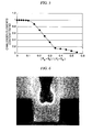
- FIG. 4 is a diagram showing a relationship between coverage ratio (t B / t i ), sputtering rate, and the ratio L/T of the distance L (m) between the target 3 and the specimen 2 with respect to the diameter T (m) of the target 3.
- the coverage ratio (t B /t i ) refers to a ratio of the film thickness (t B ) of the chalcogenide film formed on the bottom surface of the enlarged diameter section 13a with respect to the film thickness (t i ) of the chalcogenide film formed on the insulating layer 12 outside the enlarged diameter section 13a, when forming the chalcogenide film on the insulating layer 12 including the contact hole 13.
- L/T is not less than 0.5 in the case where the coverage ratio (t B / t i ) is not less than 0.7 in order to ensure the in-plane homogeneity of the chalcogenide film. Moreover, L/T is not more than 1.5 in the case where sputtering rate is 1.0 while taking the productivity of the chalcogenide film into consideration. Therefore, the L/T range that satisfies both of the coverage ratio (t B / t i ) and the sputtering rate is not less than 0.5 and not more than 1.5, preferably not less than 0.7 and not more than 1.3.
- the composition of the chalcogenide film is Ge 2 Sb 2 Te 5 .
- the ratio of the contained chalcogen elements such as Ge and Te rapidly decreases when (P s ⁇ S i ) / (P t ⁇ S s ) exceeds 0.1, and the ratio of the contained chalcogen elements significantly decreases to 0.2 or less when (P s ⁇ S t ) / (P t ⁇ S s ) further exceeds 0.35.
- SEM scanning type electron microscope
- SEM scanning type electron microscope
- the ratio L/T of the distance L with respect to the diameter T of the target 3 is not less than 0.5 and not more than 1.5. Consequently, it is possible, in a state where the sputtering rate is maintained at an optimum condition, to form, within the enlarged diameter section 13a of the contact hole 13, a dense chalcogenide film 17 with a stoichiometric composition, having no defects such as gaps and cracks therein.
- the present invention may be utilized in forming a dense chalcogenide film with a stoichiometric composition, having no defects such as gaps and cracks therein, and may also be utilized in manufacturing a resistance variable type recording element having such a chalcogenide film that serves as a recording layer.
Landscapes
- Chemical & Material Sciences (AREA)
- Engineering & Computer Science (AREA)
- Chemical Kinetics & Catalysis (AREA)
- Materials Engineering (AREA)
- Mechanical Engineering (AREA)
- Metallurgy (AREA)
- Organic Chemistry (AREA)
- Manufacturing & Machinery (AREA)
- Inorganic Chemistry (AREA)
- General Chemical & Material Sciences (AREA)
- Semiconductor Memories (AREA)
- Physical Vapour Deposition (AREA)
Abstract
Description
- The present invention relates to a method for forming a chalcogenide film by means of sputtering, and in more detail, relates to a method for forming, by means of sputtering, a dense chalcogenide film with a stoichiometric composition that is suitably used for a recording layer of a highly integrated memory such as phase change memory capable of nonvolatile operation, and that has no defects such as gaps and cracks therein.
The present invention also relates to a method for manufacturing a recording element including the above method for forming a chalcogenide film, and in particular, to a method for manufacturing a resistance variable type recording element.
The present patent application claims priority based on Japanese Patent Application No.2007-15059, filed January 25, 2007 - In recent years, in mobile devices such as mobile telephones and mobile information terminals, there has been an increasing need for handling a large amount of information such as image data. Also in memory elements to be installed in these mobile devices there has been an increasing demand for a high speed, low power consumption, and small nonvolatile memory with a large capacity. In particular, a resistance variable type nonvolatile memory (resistance variable type recording element) which uses a chalcogen compound whose resistance changes depending on its crystal condition, has been drawing attention as a memory that is highly integrated and capable of nonvolatile operation (for example, refer to Patent Document 1).
This resistance variable type nonvolatile memory has a simple structure in which two electrodes sandwich a chalcogenide film that serves as a recording layer, and is capable of stably maintaining the recording state thereof even at room temperature. Therefore it is an excellent memory sufficiently capable of holding memory for more than ten years.
[Patent Document 1] Japanese Unexamined Patent Application, First Publication No.2004-348906 - Incidentally, in a conventional resistance variable type nonvolatile memory, if the size of the elements is simply miniaturized in order to achieve high integration, the gap between adjacent elements becomes extremely narrow. Therefore, there has been a problem in that for example if, in order to cause a phase change in a recording layer of a single element, a predetermined electric voltage is applied to electrodes thereabove and therebelow, the heat emitted from the lower electrode may have a negative influence on the adjacent elements.
- Consequently, there may be considered a structure where an insulating layer with a low thermal conductivity is formed on a substrate, and a hole with a small diameter is formed in this insulating layer and a chalcogen compound is embedded within this hole, to thereby separate the elements. However, in this structure, it is difficult to densely embed a chalcogen compound in the hole, and it is difficult to obtain a dense chalcogenide film.
Moreover, since the chalcogen compound contains volatile chalcogen elements, a part of the volatile chalcogen elements is volatilized during the film forming process, and the composition of the obtained chalcogenide film is deviated from its stoichiometric composition. Therefore it is difficult to form a chalcogenide film in a state in which its stoichiometric composition is maintained. - The present invention has been achieved in order to solve the above problems, with an object of providing a method for forming a chalcogenide film by means of sputtering, capable of forming a dense chalcogenide film with a stoichiometric composition, having no defects such as gaps and cracks therein.
A further object of the present invention is to provide a method for manufacturing a recording element by applying the above chalcogenide film forming method. - The present inventors earnestly investigated the method of forming a chalcogenide film by means of sputtering, and as a result, discovered that when forming a chalcogenide film within a contact hole in an insulating layer by means of sputtering, in a case where a target having a composition the same as that of the chalcogenide film is used and the diameter of this target is T (m) and the distance between this target and the substrate is L (m), if the ratio L/T of the distance with respect to the diameter of the target is not less than 0.5 and not more than 1.5, it is possible to form a dense chalcogenide film with a stoichiometric composition, having no defects such as gaps and cracks therein. Consequently, the present inventors have completed the present invention.
- The present invention provides a method for forming a chalcogenide film within a contact hole formed in an insulating layer on a substrate, the method including: preparing a target having a composition the same as that of the chalcogenide film; setting a ratio L/T of a distance L with respect to a diameter T of the target to a value not less than 0.5 and not more than 1.5, where the diameter of the target is T (m) and the distance between the target and the substrate is L (m); and forming a chalcogenide film within the contact hole by a sputtering process in which a bias electric power is applied to the substrate and a sputtering electric power is applied to the target.
- Furthermore, the present invention provides a method for manufacturing a recording element that includes a chalcogenide film, the method including: forming, on a substrate, an insulating layer having a contact hole with an enlarged diameter upper section; forming a first electrode within the contact hole; preparing a target having a composition the same as that of the chalcogenide film; setting a ratio L/T of a distance L with respect to a diameter T of the target to a value not less than 0.5 and not more than 1.5, where the diameter of the target is T (m) and the distance between the target and the substrate is L (m); forming, on the first electrode, a chalcogenide film that serves as a recording layer, by a sputtering process in which a bias electric power is applied to the substrate and a sputtering electric power is applied to the target; and forming a second electrode on the chalcogenide film.
- In the above method for forming a chalcogenide film and the method for manufacturing a recording element, it is preferable that in a case where a surface area of the substrate is Ss (cm2), a bias electric power thereof is Ps (W), a surface area of the target is St (cm2), and a sputtering electric power thereof is Pt (W), a ratio Ds / Dt of a power density Ds of the substrate with respect to a power density Dt of the target satisfy the following expression (1):

- Preferably the power density Ds of the substrate and the power density Dt of the target are optimized to thereby densely fill in the contact hole with the chalcogenide film, while maintaining a stoichiometric composition thereof.
Preferably the chalcogenide film includes a chalcogen compound containing at least one element selected from the group consisting of S, Se, and Te.
Preferably the chalcogen compound contains: Te not less than 30% by weight and not more than 60% by weight; Ge not less than 10% by weight and not more than 70% by weight; Sb not less than 10% by weight and not more than 40%; and Se not less than 10% by weight and not more than 70%, and the total content ratio of these Te, Ge, Sb, and Se is not more than 100% by weight. - Preferably the first and second electrodes contain at least one element selected from the group consisting of Ti, Zr, Hf, V, Nb, Ta, Cr, Mo, W, Ru, Pt, and Ir.
- According to the method of the present invention for forming a chalcogenide film by means of sputtering, in a case where the diameter of the target having a composition the same as that of the chalcogenide film is T (m) and the distance between this target and the substrate is L (m), the ratio L/T of the distance L with respect to the diameter T of the target is not less than 0.5 and not more than 1.5. Consequently, it is possible, in a state where the sputtering rate is maintained at an optimum condition, to form, within the contact hole in the insulating layer, a dense chalcogenide film with a stoichiometric composition, having no defects such as gaps and cracks therein.
Moreover, a bias electric power is applied to the substrate and a sputtering electric power is applied to the target. As a result it is possible to form a dense chalcogenide film in a state where the composition of the film containing volatile chalcogen elements maintains its stoichiometric composition. - According to the method of the present invention for manufacturing a recording element that includes the chalcogenide film as a recording layer, in a case where the diameter of the target having a composition the same as that of the chalcogenide film is T (m) and the distance between this target and the substrate is L (m), the ratio L/T of the distance L with respect to the diameter T of the target is not less than 0.5 and not more than 1.5. Consequently, it is possible, in a state where the sputtering rate is maintained at an optimum condition, to form, within the contact hole, a dense chalcogenide film with a stoichiometric composition, having no defects such as gaps and cracks therein.
Moreover, a bias electric power is applied to the substrate and a sputtering electric power is applied to the target. As a result it is possible to form a dense chalcogenide film in a state where the composition of the film containing volatile chalcogen elements maintains its stoichiometric composition.
Therefore, it is possible to provide a recording element in which the recording layer is formed with a dense chalcogenide film with a stoichiometric composition, having no defects such as gaps and cracks thereinside. -
-
FIG. 1 is a schematic sectional view showing a sputtering apparatus used in a method for forming a chalcogenide film by means of sputtering, according to an embodiment of the present invention. -
FIG. 2 is a sectional view showing a silicon wafer used in manufacturing a phase change type memory. -
FIG. 3 is a sectional view showing a phase change type memory of the present embodiment formed on a silicon wafer. -
FIG. 4 is a diagram showing a relationship between coverage ratio (tB /ti), sputtering rate, and L/T. -
FIG. 5 is a diagram showing a relationship between content ratio of chalcogen elements in a chalcogenide film, and (Ps × St) / (Pt × Ss) (= Ds / Dt). -
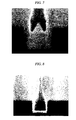
FIG. 6 is a scanning type electron microscope image showing a sectional shape of a chalcogenide film in a case where the chalcogenide film is formed by means of sputtering while a bias electric power Ps (W) is being applied to a specimen. -
FIG. 7 is a scanning type electron microscope image showing a sectional shape of a chalcogenide film in a case where the chalcogenide film is formed by means of sputtering without a bias electric power Ps (W) being applied to the specimen. -
FIG. 8 is a scanning type electron microscope image showing a sectional shape of a chalcogenide film formed by means of a conventional sputtering method. - 1: cooling stage with electrostatic chuck, 2: specimen, 3: target, 4: magnet, 5, 6: power supply, 11: silicon wafer, 12: insulating layer, 13: contact hole, 13a: enlarged diameter section, 14: tungsten, 15: titanium nitride (TiN), 16: lower electrode (first electrode), 17: chalcogenide film, 18: upper electrode (second electrode)
- There is described a best mode for carrying out a method for forming a chalcogenide film by means of sputtering of the present invention.
This mode is to give a specific description for a better understanding of the intent of the invention, and should not be construed as limiting the present invention unless otherwise stated. -
FIG. 1 is a schematic sectional view showing a sputtering apparatus used in a method for forming a chalcogenide film by means of sputtering, according to an embodiment of the present invention. In this drawing:reference symbol 1 denotes a cooling stage with an electrostatic chuck provided within a vacuum chamber (not shown in the drawing);reference symbol 2 denotes a specimen formed with a disk shaped substrate that is adsorbed and fixed on the cooling stage with the electrostatic chuck, by an electrostatic force;reference symbol 3 denotes a target arranged opposite to the upper surface of thespecimen 2;reference symbol 4 denotes a magnet that is provided on the upper section side of thetarget 3 so as to fix thetarget 3 with magnetic force;reference symbol 5 denotes a power supply that applies a bias electric power Ps (W) to thespecimen 2; andreference symbol 6 denotes a power supply that applies a sputtering electric power Pt(W) to thetarget 3. - If the distance between this
target 3 and thespecimen 2 is L (m) and the diameter of thistarget 3 is T (m), the ratio L/T of this distance L and the diameter T of thetarget 3 is adjusted to be not less than 0.5 and not more than 1.5, preferably, not less than 0.7 and not more than 1.3. - For this
target 3, a target material consisting of a chalcogen compound, which is a material having a composition the same as that of the chalcogenide film to be formed is suitable, and specific examples of this chalcogen compound include a chalcogen compound containing at least one element selected from a group consisting of S, Se, and Te. More specifically, examples of this include a chalcogen compound containing: Te not less than 30% by weight and not more than 60% by weight; Ge not less than 10% by weight and not more than 70% by weight; Sb not less than 10% by weight and not more than 40%; and Se not less than 10% by weight and not more than 70%, and the total content ratio of these Te, Ge, Sb, and Se is not more than 100% by weight.
Specific examples of this chalcogen compound include Ge2Sb2Te5, GeSb2Te5, and GeSe. - The
specimen 2 may have a contact hole for forming the chalcogenide film, and for example, a silicon wafer (substrate) 11 shown inFIG. 2 is suitable therefor.
Thissilicon wafer 11 is a wafer used in manufacturing a phase change type memory (resistance variable type recording element) with a chalcogenide film serving as a recording layer, in which, on aninsulating layer 12 made of silicon oxide formed on a semiconductor circuit or the like (not shown in the drawing) of a silicon substrate, there is formed acontact hole 13 that reaches this semiconductor circuit, and an upper section of thiscontact hole 13 has an enlarged diameter and serves as an enlargeddiameter section 13a. Within thecontact hole 13 except for this enlargeddiameter section 13a, there is formed a lower electrode (first electrode) 16 of the phase change type memory having a two-layer structure of tungsten (W) 14 and titanium nitride (TiN) 15. - This
lower electrode 16, as with an upper electrode (second electrode) 18 formed on the chalcogenide film described later, may be electrically conductive, and in addition to the above composition, any one of a metal, an alloy metal, a metallic oxide, and a metallic nitride with an electrically conductive property containing at least one type of material selected from the group consisting of Ti, Zr, Hf, V, Nb, Ta, Cr, Mo, W, Ru, Pt, and Ir, may preferably be used. - Next, with use of the above sputtering apparatus, the chalcogenide film is formed within the enlarged
diameter section 13a of thesilicon wafer 11 shown inFIG. 2 .
In this film formation, in order to form a dense chalcogenide film in a state where the composition of the film containing volatile chalcogen elements maintains its stoichiometric composition, a bias electric power Ps (W) is applied to thespecimen 2 with use of thepower supply 5 and a sputtering electric power Pt (W) is applied to thetarget 3 with use of thepower supply 6. - In order to optimize these bias electric power Ps (W) and sputtering electric power Pt (W), when the surface area of the
specimen 2 is St (cm2), the bias electric power thereof is Ps (W), the surface area of thetarget 3 is St (cm2), and the sputtering electric power thereof is Pt (W), the ratio Ds / Dt of the power density Ds of thespecimen 2 with respect to the power density Dt of thetarget 3 needs to satisfy the following expression (1):
- By optimizing these bias electric power Ps (W) and sputtering electric power Pt (W), volatilization of volatile chalcogen elements is suppressed to a minimum. Therefore the composition of the chalcogenide film to be formed becomes the same as that of the
target 3, while the stoichiometric composition of the chalcogenide film is maintained. Moreover, it becomes unlikely to have a gap or the like within the film, and therefore the density of the film is improved.
As a result, as shown inFIG. 3 , within theenlarged diameter section 13a of thesilicon wafer 11 there is formed adense chalcogenide film 17 that has an extremely low level of defects such as gaps and that maintains its stoichiometric composition. Thischalcogenide film 17, in the case of the phase change type memory, becomes a recording layer and has excellent flatness. Therefore chemical mechanical polishing (CMP) or the like is not required. - Next, on this
chalcogenide film 17 there is formed an upper electrode (second electrode) 18. Thisupper electrode 18, as with thelower electrode 16, may be electrically conductive, and for example, may be an electrode having a two-layer structure of tungsten (W) and titanium nitride (TiN), or preferably has a single layer structure or a lamination structure formed with any one of a metal, an alloy metal, a metallic oxide, and a metallic nitride with an electrically conductive property containing at least one type of material selected from the group consisting of Ti, Zr, Hf, V, Nb, Ta, Cr, Mo, W, Ru, Pt, and Ir.
Thereby, it is possible to manufacture a phasechange type memory 19 with thechalcogenide film 17 serving as a recording layer. - Next, there are described results of an experiment carried out by the present inventors, regarding the method of forming a chalcogenide film by means of sputtering according to the present embodiment.
FIG. 4 is a diagram showing a relationship between coverage ratio (tB / ti), sputtering rate, and the ratio L/T of the distance L (m) between thetarget 3 and thespecimen 2 with respect to the diameter T (m) of thetarget 3. Here the coverage ratio (tB /ti) refers to a ratio of the film thickness (tB) of the chalcogenide film formed on the bottom surface of theenlarged diameter section 13a with respect to the film thickness (ti) of the chalcogenide film formed on the insulatinglayer 12 outside theenlarged diameter section 13a, when forming the chalcogenide film on the insulatinglayer 12 including thecontact hole 13. - Referring to
FIG. 4 , L/T is not less than 0.5 in the case where the coverage ratio (tB / ti) is not less than 0.7 in order to ensure the in-plane homogeneity of the chalcogenide film. Moreover, L/T is not more than 1.5 in the case where sputtering rate is 1.0 while taking the productivity of the chalcogenide film into consideration. Therefore, the L/T range that satisfies both of the coverage ratio (tB / ti) and the sputtering rate is not less than 0.5 and not more than 1.5, preferably not less than 0.7 and not more than 1.3. -
FIG. 5 is a diagram showing a relationship between content ratio of chalcogen elements in the chalcogenide film and (Ps × St) / (Pt × Ss) (= Ds / Dt).
Here, the composition of the chalcogenide film is Ge2Sb2Te5.
Referring toFIG. 5 , it can be seen that the ratio of the contained chalcogen elements such as Ge and Te rapidly decreases when (Ps × Si) / (Pt × Ss) exceeds 0.1, and the ratio of the contained chalcogen elements significantly decreases to 0.2 or less when (Ps × St) / (Pt × Ss) further exceeds 0.35. -
FIG. 6 is a scanning type electron microscope (SEM) image showing the sectional shape of a chalcogenide film within theenlarged diameter section 13a in a case where the chalcogenide film is formed by means of sputtering while applying a bias electric power Ps (W) to thespecimen 2 under a condition of L/T = 1.0.
FIG. 7 is a scanning type electron microscope (SEM) image showing the sectional shape of a chalcogenide film within theenlarged diameter section 13a in a case where the chalcogenide film is formed by means of sputtering while applying no bias electric power Ps (W) to thespecimen 2 under a condition of L/T =1.0.
FIG. 8 is a scanning type electron microscope (SEM) image showing the sectional shape of a chalcogenide film within theenlarged diameter section 13a in a case where the chalcogenide film is formed on thespecimen 2 by means of sputtering under a condition of L/T = 0.2, which is a conventional sputtering method. - According to these diagrams, it is understood that in the case where a bias electric power Ps (W) is applied to the
specimen 2, a predetermined thickness is ensured for the chalcogenide film formed within theenlarged diameter section 13a, the surface thereof is flattened, and the quality of the film is excellent.
Moreover, it is understood that in the case where a bias electric power Ps (W) is not applied to thespecimen 2, while a conically shaped protrusion is formed on the surface of the chalcogenide film formed within theenlarged diameter section 13 a, a predetermined thickness is ensured, the surface thereof is flattened, and the quality of the film is excellent.
On the other hand, in the case of the conventional example, the thickness of the chalcogenide film formed within theenlarged diameter section 13a is extremely thin, the electrical characteristic of the film is significantly inconsistent, and the quality of the film is inferior. - As described above, according to the method for forming a chalcogenide film by means of sputtering according to the present embodiment, in the case where the diameter of the
target 3 having a composition the same as that of the chalcogenide film is T (m) and the distance between thistarget 3 and thespecimen 2 is L (m), the ratio L/T of the distance L with respect to the diameter T of thetarget 3 is not less than 0.5 and not more than 1.5. Consequently, it is possible, in a state where the sputtering rate is maintained at an optimum condition, to form, within theenlarged diameter section 13a of thecontact hole 13, adense chalcogenide film 17 with a stoichiometric composition, having no defects such as gaps and cracks therein. - Moreover, since a bias electric power is applied to the
specimen 2, it is possible, in a state where the composition of the film containing volatile chalcogen elements maintains its stoichiometric composition, to form a dense chalcogenide film having a flat surface.
Therefore, it is possible to provide a resistance variable type recording element in which a recording layer is formed with a dense chalcogenide film with a stoichiometric composition, having no defects such as gaps and cracks therein. - The present invention may be utilized in forming a dense chalcogenide film with a stoichiometric composition, having no defects such as gaps and cracks therein, and may also be utilized in manufacturing a resistance variable type recording element having such a chalcogenide film that serves as a recording layer.
Claims (11)
- A method for forming a chalcogenide film within a contact hole formed in an insulating layer on a substrate,
the method comprising:preparing a target having a composition the same as that of the chalcogenide film;setting a ratio L/T of a distance L with respect to a diameter T of the target to a value not less than 0.5 and not more than 1.5, where the diameter of the target is T (m) and the distance between the target and the substrate is L (m); andforming a chalcogenide film within the contact hole by a sputtering process in which a bias electric power is applied to the substrate and a sputtering electric power is applied to the target. - A sputtering method for a chalcogenide film according to claim 1, wherein in a case where a surface area of the substrate is Ss (cm2), a bias electric power applied to the substrate is Ps (W), a surface area of the target is St (cm2), and a sputtering electric power applied to the target is Pt (W), a ratio Ds / Dt of a power density Ds of the substrate with respect to a power density Dt of the target satisfy the following expression (1):

- A method for forming a chalcogenide film according to claim 2, wherein the power density Ds of the substrate and the power density Dt of the target are optimized to thereby densely fill in the contact hole with the chalcogenide film, while maintaining a stoichiometric composition thereof.
- A method for forming a chalcogenide film according to claim 1, wherein the chalcogenide film comprises a chalcogen compound containing at least one element selected from the group consisting of S, Se, and Te.
- A method for forming a chalcogenide film according to claim 4, wherein the chalcogen compound contains: Te not less than 30% by weight and not more than 60% by weight; Ge not less than 10% by weight and not more than 70% by weight; Sb not less than 10% by weight and not more than 40%; and Se not less than 10% by weight and not more than 70%, and the total content ratio of these Te, Ge, Sb, and Se is not more than 100% by weight.
- A method for manufacturing a recording element that includes a chalcogenide film, the method comprising:forming, on a substrate, an insulating layer having a contact hole with an enlarged diameter upper section;forming a first electrode within the contact hole;preparing a target having a composition the same as that of the chalcogenide film;setting a ratio L/T of a distance L with respect to a diameter T of the target to a value not less than 0.5 and not more than 1.5, where the diameter of the target is T (m) and the distance between the target and the substrate is L (m);forming, on the first electrode, a chalcogenide film that serves as a recording layer, by a sputtering process in which a bias electric power is applied to the substrate and a sputtering electric power is applied to the target; andforming a second electrode on the chalcogenide film.
- A method for manufacturing a recording element according to claim 6, wherein in a case where a surface area of the substrate is Ss (cm2), a bias electric power applied to the substrate is Ps (W), a surface area of the target is St (cm2), and a sputtering electric power applied to the target is Pt (W), a ratio Ds / Dt of a power density Ds of the substrate with respect to a power density Dt of the target satisfy the following expression (1):

- A method for manufacturing a recording element according to claim 7, wherein the power density Ds of the substrate and the power density Dt of the target are optimized to thereby densely fill in the contact hole with the chalcogenide film, while maintaining a stoichiometric composition thereof.
- A method for manufacturing a recording element according to claim 6, wherein the chalcogenide film comprises a chalcogen compound containing at least one element selected from the group consisting of S, Se, and Te.
- A method for manufacturing a recording element according to claim 9, wherein the chalcogen compound contains: Te not less than 30% by weight and not more than 60% by weight; Ge not less than 10% by weight and not more than 70% by weight; Sb not less than 10% by weight and not more than 40%; and Se not less than 10% by weight and not more than 70%, and the total content ratio of these Te, Ge, Sb, and Se is not more than 100% by weight.
- A method for manufacturing a recording element according to claim 6, wherein the first and second electrodes contain at least one element selected from the group consisting of Ti, Zr, Hf, V, Nb, Ta, Cr, Mo, W, Ru, Pt, and Ir.
Applications Claiming Priority (2)
| Application Number | Priority Date | Filing Date | Title |
|---|---|---|---|
| JP2007015059 | 2007-01-25 | ||
| PCT/JP2008/051001 WO2008090963A1 (en) | 2007-01-25 | 2008-01-24 | Method for forming chalcogenide film and method for manufacturing recording element |
Publications (2)
| Publication Number | Publication Date |
|---|---|
| EP2109142A1 true EP2109142A1 (en) | 2009-10-14 |
| EP2109142A4 EP2109142A4 (en) | 2010-07-28 |
Family
ID=39644537
Family Applications (1)
| Application Number | Title | Priority Date | Filing Date |
|---|---|---|---|
| EP08703828A Withdrawn EP2109142A4 (en) | 2007-01-25 | 2008-01-24 | Method for forming chalcogenide film and method for manufacturing recording element |
Country Status (7)
| Country | Link |
|---|---|
| US (1) | US20100032290A1 (en) |
| EP (1) | EP2109142A4 (en) |
| JP (1) | JP5090375B2 (en) |
| KR (1) | KR101044369B1 (en) |
| CN (1) | CN101589469B (en) |
| TW (1) | TWI350528B (en) |
| WO (1) | WO2008090963A1 (en) |
Families Citing this family (3)
| Publication number | Priority date | Publication date | Assignee | Title |
|---|---|---|---|---|
| US8426242B2 (en) | 2011-02-01 | 2013-04-23 | Macronix International Co., Ltd. | Composite target sputtering for forming doped phase change materials |
| EP3245312A1 (en) * | 2015-01-12 | 2017-11-22 | Nuvosun, Inc. | High rate sputter deposition of alkali metal-containing precursor films useful to fabricate chalcogenide semiconductors |
| US12310265B2 (en) | 2022-06-21 | 2025-05-20 | International Business Machines Corporation | Dome-shaped phase change memory mushroom cell |
Family Cites Families (17)
| Publication number | Priority date | Publication date | Assignee | Title |
|---|---|---|---|---|
| JP3810452B2 (en) * | 1995-03-23 | 2006-08-16 | 株式会社アルバック | Magnetron sputter deposition system |
| US5976327A (en) * | 1997-12-12 | 1999-11-02 | Applied Materials, Inc. | Step coverage and overhang improvement by pedestal bias voltage modulation |
| JP4911845B2 (en) * | 2001-09-20 | 2012-04-04 | 株式会社リコー | Phase change nonvolatile memory element, memory array using the phase change nonvolatile memory element, and information recording method for the phase change nonvolatile memory element |
| JP2004348906A (en) | 2003-05-26 | 2004-12-09 | Hitachi Ltd | Phase change recording medium and phase change memory |
| JP2005117030A (en) * | 2003-09-17 | 2005-04-28 | Mitsubishi Materials Corp | Phase change film for semiconductor non-volatile memory and sputtering target for forming the phase change film |
| JP4766441B2 (en) * | 2003-09-17 | 2011-09-07 | 三菱マテリアル株式会社 | Phase change film for semiconductor non-volatile memory and sputtering target for forming the phase change film |
| KR100784381B1 (en) * | 2004-07-23 | 2007-12-11 | 삼성전자주식회사 | Deposition apparatus and method |
| KR100632948B1 (en) * | 2004-08-06 | 2006-10-11 | 삼성전자주식회사 | Chalcogen compound sputtering method and phase change memory device formation method using the same |
| KR100653701B1 (en) * | 2004-08-20 | 2006-12-04 | 삼성전자주식회사 | Method for forming small via structure of semiconductor device and manufacturing method of phase change memory device using same |
| DE102004041905A1 (en) * | 2004-08-30 | 2006-03-02 | Infineon Technologies Ag | Reactive sputtering process to optimize the thermal stability of thin chalcogenide layers |
| JP4687949B2 (en) * | 2004-11-10 | 2011-05-25 | 三菱マテリアル株式会社 | Method for producing target for forming phase change recording film with short pre-sputtering time |
| EP1710324B1 (en) * | 2005-04-08 | 2008-12-03 | STMicroelectronics S.r.l. | PVD process and chamber for the pulsed deposition of a chalcogenide material layer of a phase change memory device |
| KR100650752B1 (en) * | 2005-06-10 | 2006-11-27 | 주식회사 하이닉스반도체 | Phase change memory device and manufacturing method thereof |
| KR100650753B1 (en) * | 2005-06-10 | 2006-11-27 | 주식회사 하이닉스반도체 | Phase change memory device and manufacturing method thereof |
| US20070007505A1 (en) * | 2005-07-07 | 2007-01-11 | Honeywell International Inc. | Chalcogenide PVD components |
| JP2007015059A (en) | 2005-07-08 | 2007-01-25 | Rinkosha:Kk | Adapter for connecting fin cutter of tube material |
| US8500963B2 (en) * | 2006-10-26 | 2013-08-06 | Applied Materials, Inc. | Sputtering of thermally resistive materials including metal chalcogenides |
-
2008
- 2008-01-24 JP JP2008555107A patent/JP5090375B2/en active Active
- 2008-01-24 KR KR1020097016430A patent/KR101044369B1/en active Active
- 2008-01-24 US US12/524,221 patent/US20100032290A1/en not_active Abandoned
- 2008-01-24 WO PCT/JP2008/051001 patent/WO2008090963A1/en not_active Ceased
- 2008-01-24 CN CN200880002896XA patent/CN101589469B/en active Active
- 2008-01-24 EP EP08703828A patent/EP2109142A4/en not_active Withdrawn
- 2008-01-25 TW TW097102928A patent/TWI350528B/en active
Also Published As
| Publication number | Publication date |
|---|---|
| US20100032290A1 (en) | 2010-02-11 |
| EP2109142A4 (en) | 2010-07-28 |
| TWI350528B (en) | 2011-10-11 |
| CN101589469A (en) | 2009-11-25 |
| JPWO2008090963A1 (en) | 2010-05-20 |
| CN101589469B (en) | 2013-03-20 |
| TW200847147A (en) | 2008-12-01 |
| KR20090101296A (en) | 2009-09-24 |
| KR101044369B1 (en) | 2011-06-29 |
| JP5090375B2 (en) | 2012-12-05 |
| WO2008090963A1 (en) | 2008-07-31 |
Similar Documents
| Publication | Publication Date | Title |
|---|---|---|
| US9006698B2 (en) | Variable resistance element and method of manufacturing the same | |
| US7820996B2 (en) | Nonvolatile memory device made of resistance material and method of fabricating the same | |
| EP2481084B1 (en) | Memory device with enhanced isolation of memory cells and a method of forming the same | |
| US8530321B2 (en) | Variable resistance element and manufacturing method thereof | |
| US7675053B2 (en) | Memory device comprising a memory layer and a metal chalcogenide ion-source layer | |
| US20090078926A1 (en) | Phase change memory device and fabrication method thereof | |
| WO2006075574A1 (en) | Resistance change element and manufacturing method thereof | |
| TW200952228A (en) | Phase change material with filament electrode | |
| CN102629661A (en) | Composite target sputtering for formation of doped phase change materials | |
| TW200830545A (en) | Phase-change material layer and phase-change memory device including the phase-change material layer | |
| JP5572749B2 (en) | Nonvolatile memory element and manufacturing method thereof | |
| US20100032290A1 (en) | Method for forming chalcogenide film and method for manufacturing recording element | |
| CN106997924B (en) | Phase transition storage and its manufacturing method and electronic equipment | |
| JPWO2009044769A1 (en) | Chalcogenide film and method for producing the same | |
| US8431922B2 (en) | Lateral phase change memory | |
| TW202135350A (en) | Electronic devices comprising metal oxide materials and related methods and systems | |
| US20250185258A1 (en) | Phase change memory with partial sidewall spacer contact | |
| US20100283025A1 (en) | Phase change devices | |
| TW201108307A (en) | Self-converging bottom electrode ring |
Legal Events
| Date | Code | Title | Description |
|---|---|---|---|
| PUAI | Public reference made under article 153(3) epc to a published international application that has entered the european phase |
Free format text: ORIGINAL CODE: 0009012 |
|
| 17P | Request for examination filed |
Effective date: 20090825 |
|
| AK | Designated contracting states |
Kind code of ref document: A1 Designated state(s): AT BE BG CH CY CZ DE DK EE ES FI FR GB GR HR HU IE IS IT LI LT LU LV MC MT NL NO PL PT RO SE SI SK TR |
|
| DAX | Request for extension of the european patent (deleted) | ||
| A4 | Supplementary search report drawn up and despatched |
Effective date: 20100629 |
|
| RIC1 | Information provided on ipc code assigned before grant |
Ipc: C23C 14/34 20060101ALI20120210BHEP Ipc: H01L 27/105 20060101AFI20120210BHEP Ipc: H01L 45/00 20060101ALI20120210BHEP |
|
| 17Q | First examination report despatched |
Effective date: 20120302 |
|
| STAA | Information on the status of an ep patent application or granted ep patent |
Free format text: STATUS: THE APPLICATION IS DEEMED TO BE WITHDRAWN |
|
| 18D | Application deemed to be withdrawn |
Effective date: 20160225 |