EP2107611A1 - Field effect transistor with Ti adhesion layer under the gate electrode - Google Patents
Field effect transistor with Ti adhesion layer under the gate electrode Download PDFInfo
- Publication number
- EP2107611A1 EP2107611A1 EP09250294A EP09250294A EP2107611A1 EP 2107611 A1 EP2107611 A1 EP 2107611A1 EP 09250294 A EP09250294 A EP 09250294A EP 09250294 A EP09250294 A EP 09250294A EP 2107611 A1 EP2107611 A1 EP 2107611A1
- Authority
- EP
- European Patent Office
- Prior art keywords
- gate electrode
- insulating layer
- layer
- opening
- active layer
- Prior art date
- Legal status (The legal status is an assumption and is not a legal conclusion. Google has not performed a legal analysis and makes no representation as to the accuracy of the status listed.)
- Withdrawn
Links
Images



Classifications
-
- H—ELECTRICITY
- H10—SEMICONDUCTOR DEVICES; ELECTRIC SOLID-STATE DEVICES NOT OTHERWISE PROVIDED FOR
- H10D—INORGANIC ELECTRIC SEMICONDUCTOR DEVICES
- H10D64/00—Electrodes of devices having potential barriers
- H10D64/60—Electrodes characterised by their materials
- H10D64/66—Electrodes having a conductor capacitively coupled to a semiconductor by an insulator, e.g. MIS electrodes
- H10D64/671—Electrodes having a conductor capacitively coupled to a semiconductor by an insulator, e.g. MIS electrodes the conductor having lateral variation in doping or structure
-
- H—ELECTRICITY
- H10—SEMICONDUCTOR DEVICES; ELECTRIC SOLID-STATE DEVICES NOT OTHERWISE PROVIDED FOR
- H10D—INORGANIC ELECTRIC SEMICONDUCTOR DEVICES
- H10D30/00—Field-effect transistors [FET]
- H10D30/01—Manufacture or treatment
- H10D30/015—Manufacture or treatment of FETs having heterojunction interface channels or heterojunction gate electrodes, e.g. HEMT
-
- H—ELECTRICITY
- H10—SEMICONDUCTOR DEVICES; ELECTRIC SOLID-STATE DEVICES NOT OTHERWISE PROVIDED FOR
- H10D—INORGANIC ELECTRIC SEMICONDUCTOR DEVICES
- H10D30/00—Field-effect transistors [FET]
- H10D30/40—FETs having zero-dimensional [0D], one-dimensional [1D] or two-dimensional [2D] charge carrier gas channels
- H10D30/47—FETs having zero-dimensional [0D], one-dimensional [1D] or two-dimensional [2D] charge carrier gas channels having two-dimensional [2D] charge carrier gas channels, e.g. nanoribbon FETs or high electron mobility transistors [HEMT]
- H10D30/471—High electron mobility transistors [HEMT] or high hole mobility transistors [HHMT]
- H10D30/475—High electron mobility transistors [HEMT] or high hole mobility transistors [HHMT] having wider bandgap layer formed on top of lower bandgap active layer, e.g. undoped barrier HEMTs such as i-AlGaN/GaN HEMTs
-
- H—ELECTRICITY
- H10—SEMICONDUCTOR DEVICES; ELECTRIC SOLID-STATE DEVICES NOT OTHERWISE PROVIDED FOR
- H10D—INORGANIC ELECTRIC SEMICONDUCTOR DEVICES
- H10D30/00—Field-effect transistors [FET]
- H10D30/60—Insulated-gate field-effect transistors [IGFET]
- H10D30/67—Thin-film transistors [TFT]
- H10D30/6729—Thin-film transistors [TFT] characterised by the electrodes
- H10D30/6737—Thin-film transistors [TFT] characterised by the electrodes characterised by the electrode materials
- H10D30/6738—Schottky barrier electrodes
-
- H—ELECTRICITY
- H10—SEMICONDUCTOR DEVICES; ELECTRIC SOLID-STATE DEVICES NOT OTHERWISE PROVIDED FOR
- H10D—INORGANIC ELECTRIC SEMICONDUCTOR DEVICES
- H10D30/00—Field-effect transistors [FET]
- H10D30/60—Insulated-gate field-effect transistors [IGFET]
- H10D30/67—Thin-film transistors [TFT]
- H10D30/674—Thin-film transistors [TFT] characterised by the active materials
- H10D30/675—Group III-V materials, Group II-VI materials, Group IV-VI materials, selenium or tellurium
-
- H—ELECTRICITY
- H10—SEMICONDUCTOR DEVICES; ELECTRIC SOLID-STATE DEVICES NOT OTHERWISE PROVIDED FOR
- H10D—INORGANIC ELECTRIC SEMICONDUCTOR DEVICES
- H10D62/00—Semiconductor bodies, or regions thereof, of devices having potential barriers
- H10D62/80—Semiconductor bodies, or regions thereof, of devices having potential barriers characterised by the materials
- H10D62/85—Semiconductor bodies, or regions thereof, of devices having potential barriers characterised by the materials being Group III-V materials, e.g. GaAs
-
- H—ELECTRICITY
- H10—SEMICONDUCTOR DEVICES; ELECTRIC SOLID-STATE DEVICES NOT OTHERWISE PROVIDED FOR
- H10D—INORGANIC ELECTRIC SEMICONDUCTOR DEVICES
- H10D62/00—Semiconductor bodies, or regions thereof, of devices having potential barriers
- H10D62/80—Semiconductor bodies, or regions thereof, of devices having potential barriers characterised by the materials
- H10D62/85—Semiconductor bodies, or regions thereof, of devices having potential barriers characterised by the materials being Group III-V materials, e.g. GaAs
- H10D62/8503—Nitride Group III-V materials, e.g. AlN or GaN
-
- H—ELECTRICITY
- H10—SEMICONDUCTOR DEVICES; ELECTRIC SOLID-STATE DEVICES NOT OTHERWISE PROVIDED FOR
- H10D—INORGANIC ELECTRIC SEMICONDUCTOR DEVICES
- H10D64/00—Electrodes of devices having potential barriers
- H10D64/60—Electrodes characterised by their materials
- H10D64/64—Electrodes comprising a Schottky barrier to a semiconductor
-
- H—ELECTRICITY
- H10—SEMICONDUCTOR DEVICES; ELECTRIC SOLID-STATE DEVICES NOT OTHERWISE PROVIDED FOR
- H10D—INORGANIC ELECTRIC SEMICONDUCTOR DEVICES
- H10D64/00—Electrodes of devices having potential barriers
- H10D64/01—Manufacture or treatment
- H10D64/013—Manufacture or treatment of electrodes having a conductor capacitively coupled to a semiconductor by an insulator
- H10D64/01302—Manufacture or treatment of electrodes having a conductor capacitively coupled to a semiconductor by an insulator the insulator being formed after the semiconductor body, the semiconductor being silicon
- H10D64/01304—Manufacture or treatment of electrodes having a conductor capacitively coupled to a semiconductor by an insulator the insulator being formed after the semiconductor body, the semiconductor being silicon characterised by the conductor
- H10D64/01324—Manufacture or treatment of electrodes having a conductor capacitively coupled to a semiconductor by an insulator the insulator being formed after the semiconductor body, the semiconductor being silicon characterised by the conductor characterised by the sectional shape, e.g. T or inverted-T
-
- H—ELECTRICITY
- H10—SEMICONDUCTOR DEVICES; ELECTRIC SOLID-STATE DEVICES NOT OTHERWISE PROVIDED FOR
- H10D—INORGANIC ELECTRIC SEMICONDUCTOR DEVICES
- H10D64/00—Electrodes of devices having potential barriers
- H10D64/20—Electrodes characterised by their shapes, relative sizes or dispositions
- H10D64/27—Electrodes not carrying the current to be rectified, amplified, oscillated or switched, e.g. gates
- H10D64/311—Gate electrodes for field-effect devices
- H10D64/411—Gate electrodes for field-effect devices for FETs
- H10D64/511—Gate electrodes for field-effect devices for FETs for IGFETs
- H10D64/517—Gate electrodes for field-effect devices for FETs for IGFETs characterised by the conducting layers
- H10D64/518—Gate electrodes for field-effect devices for FETs for IGFETs characterised by the conducting layers characterised by their lengths or sectional shapes
Definitions
- the present invention relates to a semiconductor device which operates at a high frequency band.
- An FET(Field Effect Transistor) using compound semiconductors, such as GaN has outstanding high frequency characteristics, and is widely put in practical use as a semiconductor device which operates at a microwave band.
- This FET has the following structures, for example. That is, a GaN buffer layer is formed on a SiC substrate, and an undoped AlGaN layer which is an active layer is formed on the GaN buffer layer. On the undoped AlGaN layer, a drain electrode and a source electrode which consist of Ti/Al/Ni/Au are formed. The drain electrode and the source electrode form ohmic junctions with the undoped AlGaN layer. The drain electrode and the source electrode are formed by laminating Ti/Al/Ni/Au and removing an unnecessary portion by a lift-off method. Furthermore, between the drain electrode and the source electrode, a gate electrode which consists of Pt/Au or Ni/Au is formed. The gate electrode forms a Schottky barrier junction with the undoped AlGaN layer. The gate electrode is formed by laminating Pt/Au or Ni/Au and removing an unnecessary portion by the lift-off method.
- a layer of a GaN system is a semiconductor layer which is bad in reactivity with Pt or Ni, in the FET mentioned above, adhesion of the AlGaN layer and Pt or the AlGaN layer and Ni is not so good. For this reason, when forming the gate electrode by the lift-off method, there was a problem that the formed gate electrode was peeled off.
- a semiconductor device has a substrate, a buffer layer which is made from a material of a GaN system formed on the substrate, an active layer which is made from a material of a GaN system formed on the buffer layer, a drain electrode and a source electrode which are formed separately on the active layer and form ohmic junctions with the active layer, an insulating layer which is formed between the drain electrode and the source electrode and has an opening, a gate electrode which is formed in the opening and forms a Schottky barrier junction with the active layer, and a metal film which is formed on a surface of the insulating layer and is attached to the gate electrode firmly.
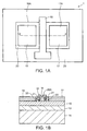
- Fig. 1A is a top view showing a structure of a semiconductor device according to this embodiment
- Fig. 1B is a cross-sectional view along dashed line A-A' of Fig. 1A .
- GaN buffer layer 12 which is made of a material of a GaN system is formed on SiC substrate 11, for example, and undoped AlGaN layer 13 which is an active layer and is made of a material of the GaN system is formed on GaN buffer layer 12.
- drain electrode 16 and source electrode 17 which form ohmic junctions with undoped AlGaN layer 13, respectively, are formed separately. Drain electrode 16 and source electrode 17 are formed of, for example, Ti/Al/Ni/Au.
- gate electrode 18 which forms a Schottky barrier junction with undoped AlGaN layer 13 is formed on undoped AlGaN layer 13.
- Gate electrode 18 is formed of, for example, Ni/Au.
- insulating layer 20 is formed on undoped AlGaN layer 13, and openings 16A, 17A and 19 in which drain electrode 16, source electrode 17 and gate electrode 18 will be formed are formed in insulating layer 20.
- Insulating layer 20 is formed of silicon nitride, for example, SiN.
- metal film 21 which consists of Ti is formed on sidewall surface 20A of opening 19 in which gate electrode 18 will be formed. Ti is excellent in adhesion with insulating layer 20 and is excellent also in adhesion with gate electrode 18.
- metal film 21 which consists of Ti with good adhesion with gate electrode 18 which consists of Ni/Au is formed on sidewall surface 20A of opening 19. For this reason, gate electrode 18 adheres to metal film 21, and gate electrode 18 is fixed firmly. Accordingly, gate electrode 18 can be prevented from being peeled off in a lift-off process at the time of forming gate electrode 18.
- a SiC substrate is used as substrate 11.
- GaN buffer layer 12 and undoped AlGaN layer 13 are laminated in this order.
- undoped AlGaN layer 13 is removed except for region 14 in which source electrode 16, drain electrode 17 and gate electrode 18 will be formed.
- insulating layer 20 is formed on a surface of GaN buffer layer 12 and a surface of undoped AlGaN layer 13, and resist 23 is further formed on insulating layer 20. And openings 22D and 22S for forming drain electrode 16 and source electrode 17 are formed in resist 23.
- insulating layer 20 is etched and openings 16A and 17A are formed in regions in which drain electrode 16 and source electrode 17 will be formed. Undoped AlGaN layer 13 is exposed in openings 16A and 17A.
- drain electrode 16 and source electrode 17 which consist of Ti/Al/Ni/Au are formed. Drain electrode 16 and source electrode 17 form ohmic junctions with undoped AlGaN layer 13.
- resist 24 is formed on a whole surface, and furthermore an opening is formed in a region in which formation of gate electrode 18 is planned at resist 24.
- insulating layer 20 is exposed.
- opening 25 is formed in insulating layer 20 by the RIE (Reactive Ion Etching) method. Opening 25 is extended outside region 14. Opening 25 does not penetrate insulating layer 20 and a depth of opening 25 does not reach undoped AlGaN layer 13 in region 14.
- metal film 21 which consists of Ti is vapor-deposited on a whole surface.
- metal film 21 is left only on sidewall surface 20A of insulating layer 20 by etchback of metal film 21. Then, resist 27 is formed. Resist 27 has opening 26 in a region in which gate electrode 18 will be formed.
- opening 19 for gate electrode formation is formed by etching and removing insulating layer 20 existing at the lower part of opening 25 by using resist 27 as a mask. Undoped AlGaN layer 13 is exposed by opening 19. Metal film 21 is not etched by this etching. Then, Ni/Au 28 is formed on a whole surface by vapor-depositting Ni and Au in order.
- gate electrode 18 which consists of Ni/Au is formed, and semiconductor device 1 is manufactured. Gate electrode 18 forms the Schottky barrier junction with undoped AlGaN layer 13. Since gate electrode 18 has good adhesion with metal film 21, gate electrode 18 adheres to metal film 21, and is fixed firmly. For this reason, when removing resist 27, gate metal 18 can be prevented from being peeled off.
- Gate electrode 18 is extended and formed on buffer layer 12 in which undoped AlGaN layer 13 is not formed. For a wire bonding process given later, width of gate electrode 19 formed on buffer layer 12 is formed more widely than width of gate electrode 18 formed on undoped AlGaN layer 13.
- overhang portion 18' of gate electrode 18 is formed above surface 20B of insulating layer 20.
- Metal film 21 which consists of Ti is formed on sidewall surface 20A of opening 19 of insulating layer 20 and on surface 20B of insulating layer 20 under overhang portion 18' of gate electrode 18.
- metal film 21 By forming metal film 21 like this, gate electrode 18 and metal film 21 adhere and are fixed in an area larger than the embodiment mentioned above. For this reason, gate electrode 18 fixed more firmly can be formed.
- overhang portion 18' of gate electrode 18 is line symmetrical with respect to center line B-B' of a region where gate electrode 18 contacts undoped AlGaN layer 13.
- overhang portion 18' of gate electrode 18 is asymmetrical with respect to center line B-B' of a region where gate electrode 18 and undoped AlGaN layer 13 contact.
- an overhang length of overhang section 18' of drain electrode 16 side is formed longer than an overhang length of overhang portion 18' of source electrode 17 side.
- metal film 21 which consists of Ti is formed on sidewall surface 20A of opening 19 of insulating layer 20 and on surface 20B of insulating layer 20 under overhang portion 18' of gate electrode 18. Therefore, as for this embodiment, an effect of the present invention is obtained.
- concentration of an electric field at gate electrode 18 edge can also be prevented by a field plate effect.
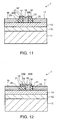
- Semiconductor device 1 of another embodiment is shown in Fig. 11 .
- metal film 21 is not formed on sidewall surface 20A of opening 19 of insulating layer 20, but metal film 21 is formed on surface 20B of insulating layer 20 under overhang portion 18' of gate electrode 18.
- gate electrode 18 also adheres to metal film 21, and gate electrode 18 fixed firmly can be formed. For this reason, in the lift-off process, when removing resist, gate electrode 18 can be prevented from being peeled off.
- semiconductor device 1 of another embodiment is shown in Fig. 12 .
- metal film 21 is not formed on sidewall surface 20A of opening 19 of insulating layer 20, but metal film 21 is formed on surface 20B of insulating layer 20 under overhang portion 18' of gate electrode 18.
- overhang potion 18' of gate electrode 18 is asymmetrical with respect to center line B-B' of a region where gate electrode 18 and undoped AlGaN layer 13 contact.
- An overhang length of overhang portion 18' of drain electrode 16 side is formed longer than an overhang length of overhang section 18' of source electrode 17 side.
- gate electrode 18 also adheres to metal film 21, and gate electrode 18 fixed firmly can be formed.
- Ni/Au was used as the material of gate electrode 18. But, when Pt/Au is used as the material for gate electrode 18, the same effect as the case where Ni/Au is used is also obtained.
- Substrate 11 may be not only the SiC substrate but a sapphire substrate etc. which are generally used. Furthermore, GaN buffer layer 12 may be a deactivated buffer layer.
Landscapes
- Junction Field-Effect Transistors (AREA)
Abstract
Description
- This application is based upon and claims the benefit of priority from the Japanese Patent Application No.
2008-092706, filed on March 31, 2008 - The present invention relates to a semiconductor device which operates at a high frequency band.
- An FET(Field Effect Transistor) using compound semiconductors, such as GaN, has outstanding high frequency characteristics, and is widely put in practical use as a semiconductor device which operates at a microwave band.
- This FET has the following structures, for example. That is, a GaN buffer layer is formed on a SiC substrate, and an undoped AlGaN layer which is an active layer is formed on the GaN buffer layer. On the undoped AlGaN layer, a drain electrode and a source electrode which consist of Ti/Al/Ni/Au are formed. The drain electrode and the source electrode form ohmic junctions with the undoped AlGaN layer. The drain electrode and the source electrode are formed by laminating Ti/Al/Ni/Au and removing an unnecessary portion by a lift-off method. Furthermore, between the drain electrode and the source electrode, a gate electrode which consists of Pt/Au or Ni/Au is formed. The gate electrode forms a Schottky barrier junction with the undoped AlGaN layer. The gate electrode is formed by laminating Pt/Au or Ni/Au and removing an unnecessary portion by the lift-off method.
- Since a layer of a GaN system is a semiconductor layer which is bad in reactivity with Pt or Ni, in the FET mentioned above, adhesion of the AlGaN layer and Pt or the AlGaN layer and Ni is not so good. For this reason, when forming the gate electrode by the lift-off method, there was a problem that the formed gate electrode was peeled off.
- In order to avoid this, a method of improving the adhesion of a gate electrode and a semiconductor substrate by forming the gate electrode with a vapor deposition rate of 2-20 Å/second is known (Japanese patent application publication No.
HEI 10-178189 - When a gate length is shortened in order to make the FET highly efficient, a bonded surface of the AlGaN layer and the gate electrode becomes small. For this reason, there is a problem that it becomes difficult to acquire sufficient adhesion also by the method mentioned above.
- The purpose of the invention is to provide an semiconductor device which can effectively prevent peeling of a gate electrode. According to one embodiment, it is provided a semiconductor device has a substrate, a buffer layer which is made from a material of a GaN system formed on the substrate, an active layer which is made from a material of a GaN system formed on the buffer layer, a drain electrode and a source electrode which are formed separately on the active layer and form ohmic junctions with the active layer, an insulating layer which is formed between the drain electrode and the source electrode and has an opening, a gate electrode which is formed in the opening and forms a Schottky barrier junction with the active layer, and a metal film which is formed on a surface of the insulating layer and is attached to the gate electrode firmly.
-
-
Fig. 1A is a top view showing a semiconductor device according to one embodiment. -
Fig. 1B is a cross-sectional view along dashed line A-A' ofFig. 1A . -
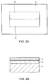
Fig. 2A is a top view showing a manufacturing process of the semiconductor device according to the embodiment. -
Fig. 2B is a cross-sectional view along dashed line A-A' ofFig. 2A . -
Fig. 3A is a top view showing the manufacturing process of the semiconductor device according to the embodiment. -
Fig. 3B is a cross-sectional view along dashed line A-A' ofFig. 3A . -
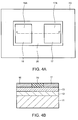
Fig. 4A is a top view showing the manufacturing process of the semiconductor device according to the embodiment. -
Fig. 4B is a cross-sectional view along dashed line A-A' ofFig. 4A . -
Fig. 5A is a top view showing the manufacturing process of the semiconductor device according to the embodiment. -
Fig. 5B is a cross-sectional view along dashed line A-A' ofFig. 5A . -
Fig. 6A is a top view showing the manufacturing process of the semiconductor device according to the embodiment. -
Fig. 6B is a cross-sectional view along dashed line A-A' ofFig. 6A . -
Fig. 7A is a top view showing the manufacturing process of the semiconductor device according to the embodiment. -
Fig. 7B is a cross-sectional view along dashed line A-A' ofFig. 7A . -
Fig. 8A is a top view showing the manufacturing process of the semiconductor device according to the embodiment. -
Fig. 7B is a cross-sectional view along dashed line A-A' of Fig. A. -
Fig. 9A is a top view showing a semiconductor device according to another embodiment. -
Fig. 9B is a cross-sectional view along dashed line A-A' ofFig. 9A . -
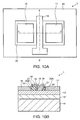
Fig. 10A is a top view showing a semiconductor device according to another embodiment. -
Fig. 10B is a cross-sectional view along dashed line A-A' ofFig. 10A . -
Fig. 11 is a cross-sectional view of a semiconductor device according to another embodiment. -
Fig. 12 is a cross-sectional view of a semiconductor device according to another embodiment. - Hereafter, the embodiments of the present invention will be explained with reference to
Fig. 1 through Fig. 12 . -
Fig. 1A is a top view showing a structure of a semiconductor device according to this embodiment, andFig. 1B is a cross-sectional view along dashed line A-A' ofFig. 1A . - In
semiconductor device 1 shown inFig. 1A and Fig. 1B ,GaN buffer layer 12 which is made of a material of a GaN system is formed onSiC substrate 11, for example, andundoped AlGaN layer 13 which is an active layer and is made of a material of the GaN system is formed onGaN buffer layer 12. Onundoped AlGaN layer 13,drain electrode 16 andsource electrode 17 which form ohmic junctions withundoped AlGaN layer 13, respectively, are formed separately.Drain electrode 16 andsource electrode 17 are formed of, for example, Ti/Al/Ni/Au. Betweendrain electrode 16 andsource electrode 17,gate electrode 18 which forms a Schottky barrier junction withundoped AlGaN layer 13 is formed onundoped AlGaN layer 13.Gate electrode 18 is formed of, for example, Ni/Au. - Here, as for
semiconductor device 1 according to this embodiment, insulatinglayer 20 is formed onundoped AlGaN layer 13, andopenings electrode 16,source electrode 17 andgate electrode 18 will be formed are formed in insulatinglayer 20. Insulatinglayer 20 is formed of silicon nitride, for example, SiN. Furthermore, onsidewall surface 20A of opening 19 in whichgate electrode 18 will be formed,metal film 21 which consists of Ti is formed. Ti is excellent in adhesion with insulatinglayer 20 and is excellent also in adhesion withgate electrode 18. - Thus, in a semiconductor device according to this embodiment,
metal film 21 which consists of Ti with good adhesion withgate electrode 18 which consists of Ni/Au, is formed onsidewall surface 20A ofopening 19. For this reason,gate electrode 18 adheres tometal film 21, andgate electrode 18 is fixed firmly. Accordingly,gate electrode 18 can be prevented from being peeled off in a lift-off process at the time of forminggate electrode 18. - Next, with reference to
Fig. 2A through Fig. 8B , a manufacturing method of the semiconductor device according to this embodiment will be explained. - First, as shown in
Fig. 2A and Fig. 2B , a SiC substrate is used assubstrate 11. Onsubstrate 11,GaN buffer layer 12 andundoped AlGaN layer 13 are laminated in this order. Then,undoped AlGaN layer 13 is removed except forregion 14 in whichsource electrode 16,drain electrode 17 andgate electrode 18 will be formed. - Next, as shown in
Fig. 3A and Fig. 3B , insulatinglayer 20 is formed on a surface ofGaN buffer layer 12 and a surface ofundoped AlGaN layer 13, and resist 23 is further formed on insulatinglayer 20. Andopenings drain electrode 16 andsource electrode 17 are formed in resist 23. - Next, using resist 23 as a mask, insulating
layer 20 is etched andopenings electrode 16 andsource electrode 17 will be formed.Undoped AlGaN layer 13 is exposed inopenings - Next, Ti, Al, Ni and Au are vapor-deposited in order. And by removing resist 23, as shown in
Fig. 4A and Fig. 4B ,drain electrode 16 andsource electrode 17 which consist of Ti/Al/Ni/Au are formed.Drain electrode 16 andsource electrode 17 form ohmic junctions withundoped AlGaN layer 13. - Next, as shown in
Fig. 5A and Fig. 5B , resist 24 is formed on a whole surface, and furthermore an opening is formed in a region in which formation ofgate electrode 18 is planned at resist 24. In an opening, insulatinglayer 20 is exposed. Then, opening 25 is formed in insulatinglayer 20 by the RIE (Reactive Ion Etching) method.Opening 25 is extended outsideregion 14.Opening 25 does not penetrate insulatinglayer 20 and a depth ofopening 25 does not reachundoped AlGaN layer 13 inregion 14. - Next, resist 24 is removed. Then, as shown in
Fig. 6A and Fig. 6B ,metal film 21 which consists of Ti is vapor-deposited on a whole surface. - Next, as shown in
Fig. 7A and Fig. 7B , in opening 25,metal film 21 is left only onsidewall surface 20A of insulatinglayer 20 by etchback ofmetal film 21. Then, resist 27 is formed. Resist 27 hasopening 26 in a region in whichgate electrode 18 will be formed. - Next, as shown in
Fig. 8A and Fig. 8B , opening 19 for gate electrode formation is formed by etching and removing insulatinglayer 20 existing at the lower part of opening 25 by using resist 27 as a mask.Undoped AlGaN layer 13 is exposed by opening 19.Metal film 21 is not etched by this etching. Then, Ni/Au 28 is formed on a whole surface by vapor-depositting Ni and Au in order. - Finally, by removing resist 27, as shown in
Fig. 1A and Fig. 1B ,gate electrode 18 which consists of Ni/Au is formed, andsemiconductor device 1 is manufactured.Gate electrode 18 forms the Schottky barrier junction withundoped AlGaN layer 13. Sincegate electrode 18 has good adhesion withmetal film 21,gate electrode 18 adheres tometal film 21, and is fixed firmly. For this reason, when removing resist 27,gate metal 18 can be prevented from being peeled off. -
Gate electrode 18 is extended and formed onbuffer layer 12 in which undopedAlGaN layer 13 is not formed. For a wire bonding process given later, width ofgate electrode 19 formed onbuffer layer 12 is formed more widely than width ofgate electrode 18 formed onundoped AlGaN layer 13. - Next, semiconductor devices according to other embodiments will be explained. In a following explanation, the same reference numbers are attached to the same parts or equivalent parts as the above-mentioned embodiment, and detailed explanations will be omitted.
- In
semiconductor device 1 of an embodiment shown inFig. 9A and Fig. 9B , overhang portion 18' ofgate electrode 18 is formed abovesurface 20B of insulatinglayer 20.Metal film 21 which consists of Ti is formed onsidewall surface 20A of opening 19 of insulatinglayer 20 and onsurface 20B of insulatinglayer 20 under overhang portion 18' ofgate electrode 18. By formingmetal film 21 like this,gate electrode 18 andmetal film 21 adhere and are fixed in an area larger than the embodiment mentioned above. For this reason,gate electrode 18 fixed more firmly can be formed.
In this embodiment, overhang portion 18' ofgate electrode 18 is line symmetrical with respect to center line B-B' of a region wheregate electrode 18 contacts undopedAlGaN layer 13. - In
semiconductor device 1 of an embodiment shown inFig. 10A and Fig. 10B , overhang portion 18' ofgate electrode 18 is asymmetrical with respect to center line B-B' of a region wheregate electrode 18 andundoped AlGaN layer 13 contact. For example, an overhang length of overhang section 18' ofdrain electrode 16 side is formed longer than an overhang length of overhang portion 18' ofsource electrode 17 side. Also in this embodiment,metal film 21 which consists of Ti is formed onsidewall surface 20A of opening 19 of insulatinglayer 20 and onsurface 20B of insulatinglayer 20 under overhang portion 18' ofgate electrode 18. Therefore, as for this embodiment, an effect of the present invention is obtained. In this embodiment, concentration of an electric field atgate electrode 18 edge can also be prevented by a field plate effect. -
Semiconductor device 1 of another embodiment is shown inFig. 11 . In thissemiconductor device 1,metal film 21 is not formed onsidewall surface 20A of opening 19 of insulatinglayer 20, butmetal film 21 is formed onsurface 20B of insulatinglayer 20 under overhang portion 18' ofgate electrode 18. In this case,gate electrode 18 also adheres tometal film 21, andgate electrode 18 fixed firmly can be formed. For this reason, in the lift-off process, when removing resist,gate electrode 18 can be prevented from being peeled off. - Furthermore,
semiconductor device 1 of another embodiment is shown inFig. 12 . In thissemiconductor device 1,metal film 21 is not formed onsidewall surface 20A of opening 19 of insulatinglayer 20, butmetal film 21 is formed onsurface 20B of insulatinglayer 20 under overhang portion 18' ofgate electrode 18. Like the embodiment shown inFig. 10 , overhang potion 18' ofgate electrode 18 is asymmetrical with respect to center line B-B' of a region wheregate electrode 18 andundoped AlGaN layer 13 contact. An overhang length of overhang portion 18' ofdrain electrode 16 side is formed longer than an overhang length of overhang section 18' ofsource electrode 17 side. In this embodiment,gate electrode 18 also adheres tometal film 21, andgate electrode 18 fixed firmly can be formed. - In the above-mentioned embodiment, Ni/Au was used as the material of
gate electrode 18. But, when Pt/Au is used as the material forgate electrode 18, the same effect as the case where Ni/Au is used is also obtained. -
Substrate 11 may be not only the SiC substrate but a sapphire substrate etc. which are generally used. Furthermore,GaN buffer layer 12 may be a deactivated buffer layer. - Other embodiments or modifications of the present invention will be apparent to those skilled in the art from consideration of the specification and practice of the invention disclosed herein. It is intended that the specification and example embodiments be considered as exemplary only, with a true scope and spirit of the invention being indicated by the following.
Claims (11)
- A semiconductor device comprising:a substrate;a buffer layer made of a material of a GaN system and formed on said substrate;an active layer made of a material of the GaN system and formed on said buffer layer;a drain electrode and a source electrode formed separately on said active layer and forming ohmic junctions with said active layer;an insulating layer formed between said drain electrode and said source electrode and formed with an opening;a gate electrode formed in said opening of said insulating layer and forming a Schottky barrier junction with said active layer; anda metal film formed on a surface of said insulating layer and adhering to said gate electrode.
- The semiconductor device according to claim 1, wherein said metal film is formed on a sidewall surface of said opening of said insulating layer.
- The semiconductor device according to claim 1, wherein said gate electrode has an overhang portion above said insulating layer and said metal film is formed between said overhang portion of said gate electrode and said insulating layer.
- The semiconductor device according to claim 3, wherein said overhang portion of said gate electrode has a drain electrode side overhang portion and a source electrode side overhang portion, and an overhang length of said drain electrode side overhang portion is longer than an overhang length of said source electrode side overhang portion.
- The semiconductor device according to any one of claim 1, 2, or 3, wherein said gate electrode is extended and formed on said buffer layer on which said active layer is not formed, and a width of said gate electrode formed on said buffer layer is wider than a width of said gate electrode formed on said active layer.
- The semiconductor device according to any one of claims 1 to 3, wherein said gate electrode is formed with a material of either Ni/Au or Pt/Au.
- A semiconductor device comprising:a substrate;a buffer layer made of a material of a GaN system formed on said substrate;an active layer made of a material of a GaN system formed on said buffer layer;a drain electrode and a source electrode formed separately on said active layer and form ohmic junctions with said active layer;an insulating layer formed between said drain electrode and said source electrode and formed with an opening;a gate electrode formed in said opening of said insulating layer and forming a Schottky barrier junction with said active layer; anda metal film formed on a sidewall surface of said opening of said insulating layer and adhering to said gate electrode.
- A semiconductor device comprising:a substrate;a buffer layer made of a material of a GaN system formed on said substrate;an active layer made of a material of a GaN system formed on said buffer layer;a drain electrode and a source electrode formed separately on said active layer and forming ohmic junctions with said active layer;an insulating layer formed between said drain electrode and said source electrode and formed with an opening;a gate electrode formed in said opening of said insulating layer and forming a Schottky barrier junction with said active layer and having an overhang portion above said insulating layer; anda metal film formed on a sidewall surface of said opening of said insulating layer, and formed on a surface of said insulating layer between said overhang portion of said gate electrode and said insulating layer, and adhering to said gate electrode.
- A semiconductor device comprising:a substrate;a buffer layer made of a material of a GaN system formed on said substrate;an active layer made of a material of a GaN system formed on said buffer layer;a drain electrode and a source electrode formed separately on said active layer and forming ohmic junctions with said active layer;an insulating layer formed between said drain electrode and said source electrode and formed with an opening,a gate electrode formed in said opening of said insulating layer and forming a Schottky barrier junction with said active layer, said gate electrode having a source electrode side overhang portion and a drain electrode side overhang portion having an overhang length longer than an overhang length of said source electrode side overhang portion above said insulating layer; anda metal film formed on a sidewall surface of said opening of said insulating layer and on a surface of said insulating layer between said drain electrode side overhang portion and said source electrode side overhang portion and said insulating layer, and adhering to said gate electrode.
- A semiconductor device comprising:a substrate;a buffer layer made of a material of a GaN system formed on said substrate;an active layer made of a material of a GaN system formed on said buffer layer;a drain electrode and a source electrode formed separately on said active layer and forming ohmic junctions with said active layer;an insulating layer formed between said drain electrode and said source electrode and formed with an opening,
a gate electrode formed in said opening of said insulating layer and forming a Schottky barrier junction with said active layer, and said gate electrode having an overhang portion above said insulating layer; anda metal film formed on a surface of said insulating layer between said overhang portion of said gate electrode and said insulating layer, and adhering to said gate electrode. - A semiconductor device comprising:a substrate;a buffer layer made of a material of a GaN system formed on said substrate;an active layer which consists of a material of a GaN system formed on said buffer layer;a drain electrode and a source electrode formed separately on said active layer and forming ohmic junctions with said active layer;an insulating layer formed between said drain electrode and said source electrode and formed with an opening;a gate electrode formed in said opening of said insulating layer and forming a Schottky barrier junction with said active layer, said gate electrode having a source electrode side overhang portion and a drain electrode side overhang portion having an overhang length longer than an overhang length of said source electrode side overhang portion above said insulating layer; anda metal film formed on the surface of said insulating layer between said source electrode side overhang portion and said drain electrode side overhang portion, and adhering to said gate electrode.
Applications Claiming Priority (1)
| Application Number | Priority Date | Filing Date | Title |
|---|---|---|---|
| JP2008092706 | 2008-03-31 |
Publications (1)
| Publication Number | Publication Date |
|---|---|
| EP2107611A1 true EP2107611A1 (en) | 2009-10-07 |
Family
ID=40756438
Family Applications (1)
| Application Number | Title | Priority Date | Filing Date |
|---|---|---|---|
| EP09250294A Withdrawn EP2107611A1 (en) | 2008-03-31 | 2009-02-05 | Field effect transistor with Ti adhesion layer under the gate electrode |
Country Status (1)
| Country | Link |
|---|---|
| EP (1) | EP2107611A1 (en) |
Cited By (1)
| Publication number | Priority date | Publication date | Assignee | Title |
|---|---|---|---|---|
| US20130288401A1 (en) * | 2012-04-27 | 2013-10-31 | Sumitomo Electric Device Innovations, Inc. | Method for fabricating semiconductor device |
Citations (4)
| Publication number | Priority date | Publication date | Assignee | Title |
|---|---|---|---|---|
| JPH05299638A (en) * | 1992-04-21 | 1993-11-12 | Toshiba Corp | Method for forming electrode wiring in compound semiconductor device |
| JPH10178189A (en) | 1996-12-16 | 1998-06-30 | Murata Mfg Co Ltd | Manufacture of semiconductor device |
| JPH11265898A (en) * | 1998-03-18 | 1999-09-28 | Hitachi Ltd | Semiconductor device and manufacturing method thereof |
| JP2007250792A (en) * | 2006-03-15 | 2007-09-27 | Furukawa Electric Co Ltd:The | Semiconductor element |
-
2009
- 2009-02-05 EP EP09250294A patent/EP2107611A1/en not_active Withdrawn
Patent Citations (4)
| Publication number | Priority date | Publication date | Assignee | Title |
|---|---|---|---|---|
| JPH05299638A (en) * | 1992-04-21 | 1993-11-12 | Toshiba Corp | Method for forming electrode wiring in compound semiconductor device |
| JPH10178189A (en) | 1996-12-16 | 1998-06-30 | Murata Mfg Co Ltd | Manufacture of semiconductor device |
| JPH11265898A (en) * | 1998-03-18 | 1999-09-28 | Hitachi Ltd | Semiconductor device and manufacturing method thereof |
| JP2007250792A (en) * | 2006-03-15 | 2007-09-27 | Furukawa Electric Co Ltd:The | Semiconductor element |
Cited By (1)
| Publication number | Priority date | Publication date | Assignee | Title |
|---|---|---|---|---|
| US20130288401A1 (en) * | 2012-04-27 | 2013-10-31 | Sumitomo Electric Device Innovations, Inc. | Method for fabricating semiconductor device |
Similar Documents
| Publication | Publication Date | Title |
|---|---|---|
| US7750369B2 (en) | Nitride semiconductor device | |
| US8004022B2 (en) | Field effect transistor | |
| US8278688B2 (en) | Compound semiconductor device and manufacturing method thereof | |
| US7829919B2 (en) | Semiconductor device | |
| JP5544713B2 (en) | Compound semiconductor device and manufacturing method thereof | |
| CN109698236B (en) | Semiconductor device | |
| US20100252863A1 (en) | Semiconductor device and manufacturing method for the same | |
| TWI814831B (en) | Semiconductor device and method of manufacturing the same | |
| US12356654B2 (en) | High electron mobility transistor and method for fabricating the same | |
| US20220278223A1 (en) | High electron mobility transistor and method for fabricating the same | |
| US12563757B2 (en) | Schottky barrier diode | |
| CN111584364B (en) | Semiconductor device manufacturing method and semiconductor device | |
| KR20190027700A (en) | Field effect transistor | |
| US20100252864A1 (en) | Semiconductor device and manufacturing method for the same | |
| JP2024504693A (en) | Lateral field effect transistor and its manufacturing method | |
| US8809907B2 (en) | Leakage barrier for GaN based HEMT active device | |
| US20100117186A1 (en) | Semiconductor device and method of producing the same | |
| US8084793B2 (en) | Microwave semiconductor device using compound semiconductor and method for manufacturing the same | |
| CN112349773A (en) | Semiconductor device and preparation method thereof | |
| CN112864241B (en) | A kind of semiconductor device and preparation method thereof | |
| JP5596636B2 (en) | Field effect transistor | |
| JP5664744B2 (en) | Compound semiconductor device and manufacturing method thereof |
Legal Events
| Date | Code | Title | Description |
|---|---|---|---|
| PUAI | Public reference made under article 153(3) epc to a published international application that has entered the european phase |
Free format text: ORIGINAL CODE: 0009012 |
|
| 17P | Request for examination filed |
Effective date: 20090211 |
|
| AK | Designated contracting states |
Kind code of ref document: A1 Designated state(s): AT BE BG CH CY CZ DE DK EE ES FI FR GB GR HR HU IE IS IT LI LT LU LV MC MK MT NL NO PL PT RO SE SI SK TR |
|
| AX | Request for extension of the european patent |
Extension state: AL BA RS |
|
| AKX | Designation fees paid |
Designated state(s): DE FR GB |
|
| 17Q | First examination report despatched |
Effective date: 20100601 |
|
| STAA | Information on the status of an ep patent application or granted ep patent |
Free format text: STATUS: THE APPLICATION IS DEEMED TO BE WITHDRAWN |
|
| 18D | Application deemed to be withdrawn |
Effective date: 20151113 |