EP2107533A2 - System und Verfahren zur Münzenauswahl - Google Patents
System und Verfahren zur Münzenauswahl Download PDFInfo
- Publication number
- EP2107533A2 EP2107533A2 EP09380046A EP09380046A EP2107533A2 EP 2107533 A2 EP2107533 A2 EP 2107533A2 EP 09380046 A EP09380046 A EP 09380046A EP 09380046 A EP09380046 A EP 09380046A EP 2107533 A2 EP2107533 A2 EP 2107533A2
- Authority
- EP
- European Patent Office
- Prior art keywords
- coin
- signal
- sender
- receiver
- edge
- Prior art date
- Legal status (The legal status is an assumption and is not a legal conclusion. Google has not performed a legal analysis and makes no representation as to the accuracy of the status listed.)
- Granted
Links
Images



Classifications
-
- G—PHYSICS
- G07—CHECKING-DEVICES
- G07D—HANDLING OF COINS OR VALUABLE PAPERS, e.g. TESTING, SORTING BY DENOMINATIONS, COUNTING, DISPENSING, CHANGING OR DEPOSITING
- G07D5/00—Testing specially adapted to determine the identity or genuineness of coins, e.g. for segregating coins which are unacceptable or alien to a currency
- G07D5/10—Testing the rim, e.g. the milling of the rim
Definitions
- the object of the present invention is a system which proves the validity of coins, tokens or in general, discoid elements through the analysis of the edge of said element.
- the present invention solves the analysis of the coin edge in a simple and economical way, and it can be incorporated in coin selectors as an additional sensor in combination with other sensors for the analysis of other characteristics, such as diameter and electric and mechanical characteristics of the alloy.
- the present invention refers to the field of devices which prove the validity of coins, tokens or other discoid elements.
- these devices determine different properties thereof such as, for example, their dimensions, electromagnetic properties, electric properties, weight, hardness, coining, among others.
- Commonly used systems are the systems which measure the dimensions of coins with optical procedures, and the ones which determine the properties of the alloy related to the electric conductivity and magnetic permeability, using one or several electromagnetic sensors.
- Other optical procedures are related to the examination of the engraving or embossing of the coins, ones pointing to the analysis of the coin faces and others pointing to the analysis of the edge or rim thereof.
- GB2071381 describes an optical sensor for coin edges comprising a sender-receiver couple whose optical beams point towards the coin, coinciding in its edge. Part of the light transmitted is reflected by the coin and reaches the sensor. According to the intensity of the light received, the coin in question will be accepted or rejected.
- This system has the inconvenience of only analyzing a small arch of the complete edge of the coin.
- WO09106072A1 describes a device for coin edge analysis consisting of the illumination of the edge by a parallel light beam, which laterally illuminates the coin edge.
- a detector On the vertical of the rolling track, there is a detector which has a focus lens and a grid coinciding with the passing of the model of the edge of the valid coin to be detected.
- the sensor will only give a valid signal when the valid diameter of the coin (through the focus lens) coincides and when the edge model also coincides.
- This sensor also has the same problem as the previous inventions, since the analysis of the edge is performed in a small arch. Another problem is that the sensor is only valid for a type of coin (with a concrete diameter and edge), and therefore, it would be necessary to include as many specific sensors as types of coins to validate.
- the effect produced by the analysis of a small part of the 360 degrees of the coin edge is that in many cases it is not possible to distinguish a coin with interrupted knurling from a flat one or one with continuous knurling and polygonal coins from circular ones. It is not possible to distinguish coins with angularly spaced inscriptions either, such as the case of the "Spanish flower” (like the €0.20 coins) or embossed patterns with a significant size or angular separation.
- the device of WO09106072A1 uses several photoreceptors oriented to different angles of the coin increasing the area of analysis. Besides being expensive, this solution presents the problem of the space required for its implementation.
- WO09744760A1 describes an optical system based on a laser light source and an optics which lightens the coin according to a vertical line perpendicular to the rolling track. In the opposite part, there is a linear sensor which is also vertical. The coin partially interrupts the beam and projects the shadow of the edge on the sensor. This enables to analyze a more important part of the coin edge, but presents the inconvenience of the high price of the sender, optics and sensor set, which makes it unfeasible in many applications.
- WO00043961A1 describes another form of edge analysis.
- the sender is a collimated laser light source to attain a beam with a rectangular section, stable with the distance.
- the result is a precise analysis of a wide area of the coin edge, but it has the inconvenience that the light source has to be located on a side of the rolling track, which is difficult to solve in small devices.
- the light source is expensive and not very strong for uses demanding a wide range of temperatures or in adverse environmental conditions.
- Said system comprises at least:
- said senders and receivers will be located on a line which is essentially parallel to the rolling track and at a minimum distance bigger than the diameter of the coin with the biggest admissible size.
- the separation between the sender and receiver is an important characteristic since it will define the area of the rolling track in which the coin edge will be examined. It is assumed that, regardless of the coin size, the area of analysis of the coin edge is equivalent, at least, to the distance between both elements of the sender-receiver set. This characteristic enables the area of the coin edge examined to be much bigger than the ones described in the state of the art and the previously mentioned ones.
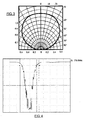
- sender and receiver An important characteristic for the sender and receiver is that they must have an important beam width, since, if not, when they are moved away from each other, there would not be an optical coupling through the reflection of the coin edge. That is to say, the sender and receiver do not have to incorporate concentrating optics. Moreover, it is convenient for the senders and receivers to have a radiation diagram approximate to the cosine law, that is to say, with a maximum (100% of the radiation transmitted for the sender or sensitivity for the receiver) in the frontal axis (0°) and a radiation minimum (0%) on the side (90°). It is also very convenient for the sender to work in the infrared spectrum and for the receiver to be exclusively suitable for said infrared radiation, so as to minimize the effects of the room light which could penetrate through the openings inside the device.
- the maximum radiation axis and sensitivity respectively are oriented towards the rolling track of the coins, that is to say, that they are both located parallel to each other and with the optical axes perpendicular to the rolling track.
- the radiation diagram defined enables the coupling with a coin during the entire path of the area of analysis. If there is no coin, there can exist a small coupling due to the reflections of a rolling channel which do not significantly affect the quality of the signal received in the device of the invention, which can be considered a controlled parameter in the mounting (offset) and which can be discriminated from the signal provided by the sensor.
- processing means of the signal comprising:
- said processing means are based on a microcontroller and, more specifically, a microcontroller such as a digital signal processor or DSP.
- said signal processing means include, at least:
- the sensor so described has the characteristic of offering safety to be able to distinguish authentic coins from fake ones, or intrusions from other coins valid in other countries.
- the system object of the present invention solves the problem of analysis in a wide area of the coin edge. For example, in a typical selector we can multiply by a factor between two and three the edge arch analyzed by this system, compared to the one known so far, being possible to analyze more than 50% of the circumference of the coin edge.
- Figure 1 schematically shows the arrangement of the sensors together with the path of the light beams in different coin positions.
- Figure 2 shows the block diagram associated to the optical sensor.
- Figure 3 shows the type of radiation diagram used for the sender and receiver of the optical sensor of the invention.
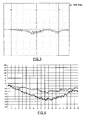
- Figure 4 shows the signal obtained at the outlet of the sensor with a coin with the technology of the previous art.
- Figure 5 shows the signal obtained with the solution proposed under the same conditions as in the previous case.
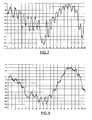
- Figure 6 shows the outlet of the amplifier (12) for two coins with different reflectivity.
- Figure 7 shows the outlet of the amplifier (12) for a coin with high relief details on its edge.
- Figure 8 shows the outlet of the amplifier (12) for a coin similar to the one shown in figure 7 but with low relief details.
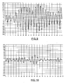
- Figure 9 shows the outlet of the band-pass filter (13) for the coin shown in figure 7 .
- Figure 10 shows the outlet of a band-pass filter (13) for the coin shown in figure 8 .
- Figure 11 shows the outlet of the amplifier (12) for a coin with a polygonal edge.
- Figure 12 shows the outlet of the amplifier (12) for a coin with a circular edge.
- Figure 13 shows the outlet of the low-pass filter (14) for the coin shown in figure 11 .
- Figure 14 shows the outlet of the low-pass filter for the coin shown in figure 12 .
- Figure 15 shows the outlet of the diverter (15) for the coin shown in figure 11 .
- Figure 16 shows the outlet of the diverter (15) for the coin shown in figure 12 .
- the system object of the present invention comprises, at least, a sender (1) which is preferably located next to the entrance (3) for the coins, while the receiver (2) is mounted next to the end (4) of the rolling ramp (6) and approximately at the same distance of said track than the sender (1).
- the distance of the optical couple to the rolling track (6) is bigger than the diameter of the biggest coin.
- the distance between the sender (1) and the receiver (2) is:
- the axes (E) of maximum radiation/sensitivity of the sender (1) and the receiver (2) have to be oriented towards the rolling ramp (6). In this way, the optical sensor of the coin edge explores the coin edge during the entire path along the measuring area.
- figure 4 represents the technology of the aforementioned art
- the form of the signal obtained has strong lateral slopes, while the useful duration of the signal is, at the most, 70ms, which at a typical speed of the coin corresponds to approximately 14mm of path.
- the start and end areas of the signal mentioned are not very useful due to their low level. Comparing this signal to the one represented in figure 5 , it can be seen the signal provided by the proposed sensor in the same conditions as the aforementioned case.
- the level is much more constant and the useful signal has a duration of 180ms, which is equivalent to 36mm of path of the coin, that is to say, more than twice than in the previous case, with the advantage that the signal is useful from start to end.
- this figure shows a schematic view of the path of the light sent by the sender (1), which is reflected on the coin (10) edge, represented in three different positions and reaches the receiver (2).
- both components, sender (1) and receiver (2) have to have such a beam width that the coupling between them is kept the same, when there is a coin on the rolling track (6).
- a typical convenient diagram for the embodiment proposed can be seen in figure 3 , where the beam width, at 50%, is about ⁇ 65°. With this diagram, it is obtained a quite planar outcome for the coupling between the sender (1), coin (10) and receiver (2), for a range of diameters of normally used coins (10).
- This characteristic remarkably facilitates extracting the useful signal from the coin edge, consisting in the variations of the signal with respect to a medium level, that is to say, the alternate modulating component which is superimposed to the medium signal which is the value of the coin reflectivity.
- the alternate component shown is caused by the reflections produced by irregularities in the coin edge, which is the main characteristic which we intend to identify or detect.
- a power source (11) controlled by a microcontroller (16) to feed the sender (1), which will be a photodiode, preferably with emission in the infrared.
- the sender (1) which will be a photodiode, preferably with emission in the infrared.
- a temperature sensor not indicated in the figures, and next to the sender (1) which can consist of a standard signal diode. According to the temperature, it is possible to control the power source of the sender (1) or else compensate the measure according to a law inverse to the thermal variation.
- the receiver (2) it is convenient that it be a high sensitivity PIN photodiode with visible light filter (transparent to the infrared). The outcome of the sensor will, be connected to the inlet of the current to voltage amplifier (transimpedance amplifier (12)) which has the advantage of linearly using the receiver (2) and optimizing the thermal behavior, as it can be seen in figure 2 .
- the device can include optical barriers (7), (8) and (9) which are normally used for measuring the diameter and position of the coin. This can be useful to analyze the signals and relate them to the position of said coin (10) on the rolling track (6).
- band-pass filtration means it is convenient to incorporate band-pass filtration means. In this way, the continuous and low frequency components disappear, remaining only the useful signal associated with the fine details of the coin edge. Given the fact that the components to be filtered are not very important, the filter is simple and for example, a second order Butterworth pass-band filter is enough, and can be incorporated through analogical means, or digital means, preferably using a microcontroller such as a digital signal processor or DSP.
- a microcontroller such as a digital signal processor or DSP.
- the system object of the present invention also comprises a second filter, namely a low-pass filter, so as to extract the low frequency components related for example to the presence of interrupted knurling, high reliefs, intrusions or polygonal coins.
- the outcome of the filter can be used directly or after passing through a diverter (15) which eliminates the direct current component and defines more precisely the flanks and slopes of the signal represented in the transitions of the different areas of the coin edge.
- the four signals that is to say, the original signal and the two filtered signals and the one derived from the second filter, are analyzed by a microcontroller (16) which calculates, for each one of them, parameters such as the medium value of the signal, the effective value (RMS), maximum and minimum peak values, peak to peak value, number of zero values (transitions), Fourier transform, separation between peaks and statistical parameters such as standard deviation and variance.
- the calculation of the parameters mentioned can be made for the entire path of the coin (10) along the rolling track (6) or for sections. In this case, optical barriers (7-9) are used to define an initial section, a central one and a final one.
- Figures 6 to 16 show examples where there are shown some of the possibilities of the system as regards coin discrimination according to the shape or details of the edge and its reflectivity.
- Figure 6 shows the outlets of two coins having the same shape and size but with different reflectivity on the edge.
- This signal (12) is analyzed directly by the microcontroller (16) and parameters such as the medium value of the signal or the minimum value can be enough to distinguish one from another.
- FIG. 7 and 8 Another example of two similar coins but with the difference of one of them featuring high relief and low relief details on the edge is shown in figures 7 and 8 respectively.
- the microcontroller will calculate for example parameters such as effective value of the signals (RMS), maximum peak value, minimum peak value, peak to peak value, number of peaks which are over a predetermined threshold, etc., being it possible to identify or discriminate coins thanks to this characteristic.
- the calculation of the parameters can be made globally for the whole signal or as it has been mentioned before, it can be made by sections, or calculating the size or separations of the details identified, since with the same sensors it is possible to associate the signal to the position of the coin at each instant.
- a third example is shown in figures 11 and 12 , where there are shown two coins, respectively, which have a similar size and material but the first one has a polygonal edge while the other one has a circular edge.
- the signals can also be used directly from the sensor (12), but it is more convenient to use those of the low-pass filter (14) outlet, which correspond to figures 13 and 14 , and, even better, those of the diverter outlet (15), figures 15 and 16 , which improves the conditions of signal analysis, eliminating the continuous component and indicating the transitions better.
- the microcontroller will calculate the parameters which will be used to discriminate the coins according to their edge characteristics.
Landscapes
- Physics & Mathematics (AREA)
- General Physics & Mathematics (AREA)
- Testing Of Coins (AREA)
Applications Claiming Priority (1)
| Application Number | Priority Date | Filing Date | Title |
|---|---|---|---|
| ES200800685A ES2346612B1 (es) | 2008-03-10 | 2008-03-10 | Sistema y metodo de seleccion de monedas. |
Publications (3)
| Publication Number | Publication Date |
|---|---|
| EP2107533A2 true EP2107533A2 (de) | 2009-10-07 |
| EP2107533A3 EP2107533A3 (de) | 2010-06-09 |
| EP2107533B1 EP2107533B1 (de) | 2017-01-04 |
Family
ID=40996713
Family Applications (1)
| Application Number | Title | Priority Date | Filing Date |
|---|---|---|---|
| EP09380046.4A Active EP2107533B1 (de) | 2008-03-10 | 2009-03-10 | System und Verfahren zur Münzenprüfung |
Country Status (2)
| Country | Link |
|---|---|
| EP (1) | EP2107533B1 (de) |
| ES (2) | ES2346612B1 (de) |
Cited By (2)
| Publication number | Priority date | Publication date | Assignee | Title |
|---|---|---|---|---|
| WO2015091561A1 (de) * | 2013-12-19 | 2015-06-25 | Novomatic Ag | Münzverarbeitungseinrichtung und zugehöriges verfahren zum klassifizieren von münzen |
| US10435220B2 (en) | 2013-12-30 | 2019-10-08 | Tetra Laval Holdings & Finance S.A. | Packaging material and packaging container having an opening device made therefrom |
Citations (8)
| Publication number | Priority date | Publication date | Assignee | Title |
|---|---|---|---|---|
| GB2071381A (en) | 1980-03-04 | 1981-09-16 | Mars Inc | Coin Testing Device |
| GB2071382A (en) | 1980-03-04 | 1981-09-16 | Mars Inc | Coin Testing Device |
| DE3335347A1 (de) | 1983-09-29 | 1985-04-11 | Siemens AG, 1000 Berlin und 8000 München | Verfahren und vorrichtung zur optoelektronischen pruefung der raendelung von muenzen |
| EP0416932A1 (de) | 1989-09-08 | 1991-03-13 | Glory Kogyo Kabushiki Kaisha | Münzprüfer |
| WO1991006072A1 (en) | 1989-10-17 | 1991-05-02 | Datalab Oy | A method and a means for recognizing a coin |
| WO1997044760A1 (en) | 1996-05-21 | 1997-11-27 | Ezio Panzeri | Coin testing apparatus and method |
| WO2000043961A1 (es) | 1999-01-25 | 2000-07-27 | Azkoyen Medios De Pago, S.A. | Metodo y aparato para la validacion y caracterizacion de monedas |
| EP1391851A1 (de) | 2002-08-22 | 2004-02-25 | Azkoyen Medios de Pago, S.A. | Verfahren und Vorrichtung zum Prüfen von Münzen |
-
2008
- 2008-03-10 ES ES200800685A patent/ES2346612B1/es active Active
-
2009
- 2009-03-10 EP EP09380046.4A patent/EP2107533B1/de active Active
- 2009-03-10 ES ES09380046.4T patent/ES2621612T3/es active Active
Patent Citations (8)
| Publication number | Priority date | Publication date | Assignee | Title |
|---|---|---|---|---|
| GB2071381A (en) | 1980-03-04 | 1981-09-16 | Mars Inc | Coin Testing Device |
| GB2071382A (en) | 1980-03-04 | 1981-09-16 | Mars Inc | Coin Testing Device |
| DE3335347A1 (de) | 1983-09-29 | 1985-04-11 | Siemens AG, 1000 Berlin und 8000 München | Verfahren und vorrichtung zur optoelektronischen pruefung der raendelung von muenzen |
| EP0416932A1 (de) | 1989-09-08 | 1991-03-13 | Glory Kogyo Kabushiki Kaisha | Münzprüfer |
| WO1991006072A1 (en) | 1989-10-17 | 1991-05-02 | Datalab Oy | A method and a means for recognizing a coin |
| WO1997044760A1 (en) | 1996-05-21 | 1997-11-27 | Ezio Panzeri | Coin testing apparatus and method |
| WO2000043961A1 (es) | 1999-01-25 | 2000-07-27 | Azkoyen Medios De Pago, S.A. | Metodo y aparato para la validacion y caracterizacion de monedas |
| EP1391851A1 (de) | 2002-08-22 | 2004-02-25 | Azkoyen Medios de Pago, S.A. | Verfahren und Vorrichtung zum Prüfen von Münzen |
Cited By (7)
| Publication number | Priority date | Publication date | Assignee | Title |
|---|---|---|---|---|
| WO2015091561A1 (de) * | 2013-12-19 | 2015-06-25 | Novomatic Ag | Münzverarbeitungseinrichtung und zugehöriges verfahren zum klassifizieren von münzen |
| CN105830127A (zh) * | 2013-12-19 | 2016-08-03 | 挪佛麦迪哥股份公司 | 硬币处理装置及对硬币进行分类的相关方法 |
| US20160314636A1 (en) * | 2013-12-19 | 2016-10-27 | Novomatic Ag | Coin processing device and corresponding method for classifying coins |
| US9691210B2 (en) | 2013-12-19 | 2017-06-27 | Novomatic Ag | Coin processing device and corresponding method for classifying coins |
| RU2671188C1 (ru) * | 2013-12-19 | 2018-10-29 | Новоматик Аг | Устройство для обработки монет и соответствующий способ классификации монет |
| CN105830127B (zh) * | 2013-12-19 | 2019-03-12 | 挪佛麦迪哥股份公司 | 硬币处理装置及对硬币进行分类的相关方法 |
| US10435220B2 (en) | 2013-12-30 | 2019-10-08 | Tetra Laval Holdings & Finance S.A. | Packaging material and packaging container having an opening device made therefrom |
Also Published As
| Publication number | Publication date |
|---|---|
| EP2107533B1 (de) | 2017-01-04 |
| ES2346612B1 (es) | 2011-08-04 |
| ES2621612T3 (es) | 2017-07-04 |
| ES2346612A1 (es) | 2010-10-18 |
| EP2107533A3 (de) | 2010-06-09 |
Similar Documents
| Publication | Publication Date | Title |
|---|---|---|
| EP2177468A1 (de) | Hilfsschleppmechanismus mit variabler Geschwindigkeit | |
| US5236074A (en) | Method and a means for recognizing a coin | |
| US20090303000A1 (en) | Linearisation of Scanned Data | |
| US9945791B2 (en) | Methods of spectroscopic analysis of diamonds and apparatuses thereof | |
| US4436196A (en) | Method of and apparatus for assessing coins | |
| CN1295698A (zh) | 监测物品用的方法和装置 | |
| EP2107533B1 (de) | System und Verfahren zur Münzenprüfung | |
| KR900006892A (ko) | 지폐식별방법 및 그 장치 | |
| JP2002157627A (ja) | 蛍光スレッド検出装置 | |
| WO2014161893A1 (en) | Coin checking | |
| US7362421B2 (en) | Analysis of signal oscillation patterns | |
| DE3305509A1 (de) | Optische muenzpruefeinrichtung | |
| US20050121619A1 (en) | Document identification system | |
| KR101758655B1 (ko) | 광학식 지폐 계수장치 | |
| GB2071382A (en) | Coin Testing Device | |
| JP3115768B2 (ja) | 硬貨判別装置 | |
| EP1383087A1 (de) | Münzunterscheidungsverfahren und -einrichtung | |
| KR100788822B1 (ko) | 기체 분자의 온도를 측정하기 위한 회전라만산란 신호분리용 광학장치 | |
| EP1164369A2 (de) | Optisches Lesegerät und optisches Leseverfahren | |
| JP4266481B2 (ja) | 硬貨識別装置 | |
| Clarke | The Laser Scanning Analyser | |
| JPH0637498Y2 (ja) | 硬貨識別装置 | |
| JPH09167269A (ja) | 硬貨識別装置 | |
| JPH01120694A (ja) | コイン識別装置 | |
| JP2002163700A (ja) | 貨幣識別装置の調整方法および装置 |
Legal Events
| Date | Code | Title | Description |
|---|---|---|---|
| PUAI | Public reference made under article 153(3) epc to a published international application that has entered the european phase |
Free format text: ORIGINAL CODE: 0009012 |
|
| AK | Designated contracting states |
Kind code of ref document: A2 Designated state(s): AT BE BG CH CY CZ DE DK EE ES FI FR GB GR HR HU IE IS IT LI LT LU LV MC MK MT NL NO PL PT RO SE SI SK TR |
|
| AX | Request for extension of the european patent |
Extension state: AL BA RS |
|
| PUAL | Search report despatched |
Free format text: ORIGINAL CODE: 0009013 |
|
| AK | Designated contracting states |
Kind code of ref document: A3 Designated state(s): AT BE BG CH CY CZ DE DK EE ES FI FR GB GR HR HU IE IS IT LI LT LU LV MC MK MT NL NO PL PT RO SE SI SK TR |
|
| AX | Request for extension of the european patent |
Extension state: AL BA RS |
|
| 17P | Request for examination filed |
Effective date: 20101118 |
|
| AKX | Designation fees paid |
Designated state(s): AT BE BG CH CY CZ DE DK EE ES FI FR GB GR HR HU IE IS IT LI LT LU LV MC MK MT NL NO PL PT RO SE SI SK TR |
|
| RAP1 | Party data changed (applicant data changed or rights of an application transferred) |
Owner name: AZKOYEN, S.A. |
|
| TPAC | Observations filed by third parties |
Free format text: ORIGINAL CODE: EPIDOSNTIPA |
|
| 17Q | First examination report despatched |
Effective date: 20151211 |
|
| GRAP | Despatch of communication of intention to grant a patent |
Free format text: ORIGINAL CODE: EPIDOSNIGR1 |
|
| INTG | Intention to grant announced |
Effective date: 20161012 |
|
| GRAS | Grant fee paid |
Free format text: ORIGINAL CODE: EPIDOSNIGR3 |
|
| GRAA | (expected) grant |
Free format text: ORIGINAL CODE: 0009210 |
|
| AK | Designated contracting states |
Kind code of ref document: B1 Designated state(s): AT BE BG CH CY CZ DE DK EE ES FI FR GB GR HR HU IE IS IT LI LT LU LV MC MK MT NL NO PL PT RO SE SI SK TR |
|
| REG | Reference to a national code |
Ref country code: GB Ref legal event code: FG4D |
|
| REG | Reference to a national code |
Ref country code: CH Ref legal event code: EP |
|
| REG | Reference to a national code |
Ref country code: AT Ref legal event code: REF Ref document number: 859917 Country of ref document: AT Kind code of ref document: T Effective date: 20170115 |
|
| REG | Reference to a national code |
Ref country code: IE Ref legal event code: FG4D |
|
| REG | Reference to a national code |
Ref country code: DE Ref legal event code: R096 Ref document number: 602009043496 Country of ref document: DE |
|
| REG | Reference to a national code |
Ref country code: LT Ref legal event code: MG4D Ref country code: NL Ref legal event code: MP Effective date: 20170104 |
|
| REG | Reference to a national code |
Ref country code: AT Ref legal event code: MK05 Ref document number: 859917 Country of ref document: AT Kind code of ref document: T Effective date: 20170104 |
|
| PG25 | Lapsed in a contracting state [announced via postgrant information from national office to epo] |
Ref country code: NL Free format text: LAPSE BECAUSE OF FAILURE TO SUBMIT A TRANSLATION OF THE DESCRIPTION OR TO PAY THE FEE WITHIN THE PRESCRIBED TIME-LIMIT Effective date: 20170104 |
|
| REG | Reference to a national code |
Ref country code: ES Ref legal event code: FG2A Ref document number: 2621612 Country of ref document: ES Kind code of ref document: T3 Effective date: 20170704 |
|
| PG25 | Lapsed in a contracting state [announced via postgrant information from national office to epo] |
Ref country code: LT Free format text: LAPSE BECAUSE OF FAILURE TO SUBMIT A TRANSLATION OF THE DESCRIPTION OR TO PAY THE FEE WITHIN THE PRESCRIBED TIME-LIMIT Effective date: 20170104 Ref country code: HR Free format text: LAPSE BECAUSE OF FAILURE TO SUBMIT A TRANSLATION OF THE DESCRIPTION OR TO PAY THE FEE WITHIN THE PRESCRIBED TIME-LIMIT Effective date: 20170104 Ref country code: NO Free format text: LAPSE BECAUSE OF FAILURE TO SUBMIT A TRANSLATION OF THE DESCRIPTION OR TO PAY THE FEE WITHIN THE PRESCRIBED TIME-LIMIT Effective date: 20170404 Ref country code: IS Free format text: LAPSE BECAUSE OF FAILURE TO SUBMIT A TRANSLATION OF THE DESCRIPTION OR TO PAY THE FEE WITHIN THE PRESCRIBED TIME-LIMIT Effective date: 20170504 Ref country code: FI Free format text: LAPSE BECAUSE OF FAILURE TO SUBMIT A TRANSLATION OF THE DESCRIPTION OR TO PAY THE FEE WITHIN THE PRESCRIBED TIME-LIMIT Effective date: 20170104 Ref country code: GR Free format text: LAPSE BECAUSE OF FAILURE TO SUBMIT A TRANSLATION OF THE DESCRIPTION OR TO PAY THE FEE WITHIN THE PRESCRIBED TIME-LIMIT Effective date: 20170405 |
|
| PG25 | Lapsed in a contracting state [announced via postgrant information from national office to epo] |
Ref country code: PL Free format text: LAPSE BECAUSE OF FAILURE TO SUBMIT A TRANSLATION OF THE DESCRIPTION OR TO PAY THE FEE WITHIN THE PRESCRIBED TIME-LIMIT Effective date: 20170104 Ref country code: AT Free format text: LAPSE BECAUSE OF FAILURE TO SUBMIT A TRANSLATION OF THE DESCRIPTION OR TO PAY THE FEE WITHIN THE PRESCRIBED TIME-LIMIT Effective date: 20170104 Ref country code: PT Free format text: LAPSE BECAUSE OF FAILURE TO SUBMIT A TRANSLATION OF THE DESCRIPTION OR TO PAY THE FEE WITHIN THE PRESCRIBED TIME-LIMIT Effective date: 20170504 Ref country code: BG Free format text: LAPSE BECAUSE OF FAILURE TO SUBMIT A TRANSLATION OF THE DESCRIPTION OR TO PAY THE FEE WITHIN THE PRESCRIBED TIME-LIMIT Effective date: 20170404 Ref country code: SE Free format text: LAPSE BECAUSE OF FAILURE TO SUBMIT A TRANSLATION OF THE DESCRIPTION OR TO PAY THE FEE WITHIN THE PRESCRIBED TIME-LIMIT Effective date: 20170104 Ref country code: LV Free format text: LAPSE BECAUSE OF FAILURE TO SUBMIT A TRANSLATION OF THE DESCRIPTION OR TO PAY THE FEE WITHIN THE PRESCRIBED TIME-LIMIT Effective date: 20170104 |
|
| REG | Reference to a national code |
Ref country code: DE Ref legal event code: R119 Ref document number: 602009043496 Country of ref document: DE |
|
| REG | Reference to a national code |
Ref country code: DE Ref legal event code: R097 Ref document number: 602009043496 Country of ref document: DE |
|
| PG25 | Lapsed in a contracting state [announced via postgrant information from national office to epo] |
Ref country code: SK Free format text: LAPSE BECAUSE OF FAILURE TO SUBMIT A TRANSLATION OF THE DESCRIPTION OR TO PAY THE FEE WITHIN THE PRESCRIBED TIME-LIMIT Effective date: 20170104 Ref country code: CZ Free format text: LAPSE BECAUSE OF FAILURE TO SUBMIT A TRANSLATION OF THE DESCRIPTION OR TO PAY THE FEE WITHIN THE PRESCRIBED TIME-LIMIT Effective date: 20170104 Ref country code: RO Free format text: LAPSE BECAUSE OF FAILURE TO SUBMIT A TRANSLATION OF THE DESCRIPTION OR TO PAY THE FEE WITHIN THE PRESCRIBED TIME-LIMIT Effective date: 20170104 Ref country code: EE Free format text: LAPSE BECAUSE OF FAILURE TO SUBMIT A TRANSLATION OF THE DESCRIPTION OR TO PAY THE FEE WITHIN THE PRESCRIBED TIME-LIMIT Effective date: 20170104 |
|
| REG | Reference to a national code |
Ref country code: CH Ref legal event code: PL |
|
| PLBE | No opposition filed within time limit |
Free format text: ORIGINAL CODE: 0009261 |
|
| STAA | Information on the status of an ep patent application or granted ep patent |
Free format text: STATUS: NO OPPOSITION FILED WITHIN TIME LIMIT |
|
| PG25 | Lapsed in a contracting state [announced via postgrant information from national office to epo] |
Ref country code: MC Free format text: LAPSE BECAUSE OF FAILURE TO SUBMIT A TRANSLATION OF THE DESCRIPTION OR TO PAY THE FEE WITHIN THE PRESCRIBED TIME-LIMIT Effective date: 20170104 Ref country code: DK Free format text: LAPSE BECAUSE OF FAILURE TO SUBMIT A TRANSLATION OF THE DESCRIPTION OR TO PAY THE FEE WITHIN THE PRESCRIBED TIME-LIMIT Effective date: 20170104 |
|
| 26N | No opposition filed |
Effective date: 20171005 |
|
| REG | Reference to a national code |
Ref country code: IE Ref legal event code: MM4A |
|
| REG | Reference to a national code |
Ref country code: FR Ref legal event code: ST Effective date: 20171130 |
|
| PG25 | Lapsed in a contracting state [announced via postgrant information from national office to epo] |
Ref country code: LU Free format text: LAPSE BECAUSE OF NON-PAYMENT OF DUE FEES Effective date: 20170310 Ref country code: DE Free format text: LAPSE BECAUSE OF NON-PAYMENT OF DUE FEES Effective date: 20171003 Ref country code: FR Free format text: LAPSE BECAUSE OF NON-PAYMENT OF DUE FEES Effective date: 20170331 |
|
| REG | Reference to a national code |
Ref country code: DE Ref legal event code: R073 Ref document number: 602009043496 Country of ref document: DE Ref country code: FR Ref legal event code: PLFP Year of fee payment: 9 |
|
| PG25 | Lapsed in a contracting state [announced via postgrant information from national office to epo] |
Ref country code: SI Free format text: LAPSE BECAUSE OF FAILURE TO SUBMIT A TRANSLATION OF THE DESCRIPTION OR TO PAY THE FEE WITHIN THE PRESCRIBED TIME-LIMIT Effective date: 20170104 Ref country code: CH Free format text: LAPSE BECAUSE OF NON-PAYMENT OF DUE FEES Effective date: 20170331 Ref country code: LI Free format text: LAPSE BECAUSE OF NON-PAYMENT OF DUE FEES Effective date: 20170331 Ref country code: IE Free format text: LAPSE BECAUSE OF NON-PAYMENT OF DUE FEES Effective date: 20170310 |
|
| REG | Reference to a national code |
Ref country code: DE Ref legal event code: R074 Ref document number: 602009043496 Country of ref document: DE |
|
| REG | Reference to a national code |
Ref country code: BE Ref legal event code: MM Effective date: 20170331 |
|
| REG | Reference to a national code |
Ref country code: FR Ref legal event code: RN Effective date: 20180216 |
|
| REG | Reference to a national code |
Ref country code: FR Ref legal event code: FC Effective date: 20180309 |
|
| PG25 | Lapsed in a contracting state [announced via postgrant information from national office to epo] |
Ref country code: DE Free format text: LAPSE BECAUSE OF NON-PAYMENT OF DUE FEES Effective date: 20171003 |
|
| PGRI | Patent reinstated in contracting state [announced from national office to epo] |
Ref country code: DE Effective date: 20180228 |
|
| PG25 | Lapsed in a contracting state [announced via postgrant information from national office to epo] |
Ref country code: BE Free format text: LAPSE BECAUSE OF NON-PAYMENT OF DUE FEES Effective date: 20170331 |
|
| REG | Reference to a national code |
Ref country code: FR Ref legal event code: PLFP Year of fee payment: 10 |
|
| PG25 | Lapsed in a contracting state [announced via postgrant information from national office to epo] |
Ref country code: FR Free format text: LAPSE BECAUSE OF NON-PAYMENT OF DUE FEES Effective date: 20170331 |
|
| PGRI | Patent reinstated in contracting state [announced from national office to epo] |
Ref country code: FR Effective date: 20180309 |
|
| PG25 | Lapsed in a contracting state [announced via postgrant information from national office to epo] |
Ref country code: MT Free format text: LAPSE BECAUSE OF NON-PAYMENT OF DUE FEES Effective date: 20170310 |
|
| PG25 | Lapsed in a contracting state [announced via postgrant information from national office to epo] |
Ref country code: HU Free format text: LAPSE BECAUSE OF FAILURE TO SUBMIT A TRANSLATION OF THE DESCRIPTION OR TO PAY THE FEE WITHIN THE PRESCRIBED TIME-LIMIT; INVALID AB INITIO Effective date: 20090310 |
|
| PG25 | Lapsed in a contracting state [announced via postgrant information from national office to epo] |
Ref country code: CY Free format text: LAPSE BECAUSE OF NON-PAYMENT OF DUE FEES Effective date: 20170104 |
|
| PG25 | Lapsed in a contracting state [announced via postgrant information from national office to epo] |
Ref country code: MK Free format text: LAPSE BECAUSE OF FAILURE TO SUBMIT A TRANSLATION OF THE DESCRIPTION OR TO PAY THE FEE WITHIN THE PRESCRIBED TIME-LIMIT Effective date: 20170104 |
|
| PG25 | Lapsed in a contracting state [announced via postgrant information from national office to epo] |
Ref country code: TR Free format text: LAPSE BECAUSE OF FAILURE TO SUBMIT A TRANSLATION OF THE DESCRIPTION OR TO PAY THE FEE WITHIN THE PRESCRIBED TIME-LIMIT Effective date: 20170104 |
|
| REG | Reference to a national code |
Ref country code: DE Ref legal event code: R082 Ref document number: 602009043496 Country of ref document: DE Representative=s name: KILBURN & STRODE LLP, NL |
|
| P01 | Opt-out of the competence of the unified patent court (upc) registered |
Effective date: 20230526 |
|
| PGFP | Annual fee paid to national office [announced via postgrant information from national office to epo] |
Ref country code: ES Payment date: 20250401 Year of fee payment: 17 |
|
| PGFP | Annual fee paid to national office [announced via postgrant information from national office to epo] |
Ref country code: GB Payment date: 20260218 Year of fee payment: 18 |
|
| PGFP | Annual fee paid to national office [announced via postgrant information from national office to epo] |
Ref country code: DE Payment date: 20260319 Year of fee payment: 18 |
|
| PGFP | Annual fee paid to national office [announced via postgrant information from national office to epo] |
Ref country code: IT Payment date: 20260324 Year of fee payment: 18 |
|
| PGFP | Annual fee paid to national office [announced via postgrant information from national office to epo] |
Ref country code: FR Payment date: 20260218 Year of fee payment: 18 |