EP2104407A1 - Capacitive/resistive devices and printed wiring boards incorporating such devices, and methods of making thereof - Google Patents
Capacitive/resistive devices and printed wiring boards incorporating such devices, and methods of making thereof Download PDFInfo
- Publication number
- EP2104407A1 EP2104407A1 EP09007939A EP09007939A EP2104407A1 EP 2104407 A1 EP2104407 A1 EP 2104407A1 EP 09007939 A EP09007939 A EP 09007939A EP 09007939 A EP09007939 A EP 09007939A EP 2104407 A1 EP2104407 A1 EP 2104407A1
- Authority
- EP
- European Patent Office
- Prior art keywords
- dielectric
- capacitive
- electrode
- resistive device
- resistive
- Prior art date
- Legal status (The legal status is an assumption and is not a legal conclusion. Google has not performed a legal analysis and makes no representation as to the accuracy of the status listed.)
- Withdrawn
Links
Images

Classifications
-
- H—ELECTRICITY
- H05—ELECTRIC TECHNIQUES NOT OTHERWISE PROVIDED FOR
- H05K—PRINTED CIRCUITS; CASINGS OR CONSTRUCTIONAL DETAILS OF ELECTRIC APPARATUS; MANUFACTURE OF ASSEMBLAGES OF ELECTRICAL COMPONENTS
- H05K1/00—Printed circuits
- H05K1/16—Printed circuits incorporating printed electric components, e.g. printed resistor, capacitor, inductor
- H05K1/167—Printed circuits incorporating printed electric components, e.g. printed resistor, capacitor, inductor incorporating printed resistors
-
- H—ELECTRICITY
- H01—ELECTRIC ELEMENTS
- H01L—SEMICONDUCTOR DEVICES NOT COVERED BY CLASS H10
- H01L27/00—Devices consisting of a plurality of semiconductor or other solid-state components formed in or on a common substrate
- H01L27/02—Devices consisting of a plurality of semiconductor or other solid-state components formed in or on a common substrate including semiconductor components specially adapted for rectifying, oscillating, amplifying or switching and having at least one potential-jump barrier or surface barrier; including integrated passive circuit elements with at least one potential-jump barrier or surface barrier
- H01L27/04—Devices consisting of a plurality of semiconductor or other solid-state components formed in or on a common substrate including semiconductor components specially adapted for rectifying, oscillating, amplifying or switching and having at least one potential-jump barrier or surface barrier; including integrated passive circuit elements with at least one potential-jump barrier or surface barrier the substrate being a semiconductor body
-
- H—ELECTRICITY
- H05—ELECTRIC TECHNIQUES NOT OTHERWISE PROVIDED FOR
- H05K—PRINTED CIRCUITS; CASINGS OR CONSTRUCTIONAL DETAILS OF ELECTRIC APPARATUS; MANUFACTURE OF ASSEMBLAGES OF ELECTRICAL COMPONENTS
- H05K1/00—Printed circuits
- H05K1/16—Printed circuits incorporating printed electric components, e.g. printed resistor, capacitor, inductor
- H05K1/162—Printed circuits incorporating printed electric components, e.g. printed resistor, capacitor, inductor incorporating printed capacitors
-
- H—ELECTRICITY
- H01—ELECTRIC ELEMENTS
- H01L—SEMICONDUCTOR DEVICES NOT COVERED BY CLASS H10
- H01L2924/00—Indexing scheme for arrangements or methods for connecting or disconnecting semiconductor or solid-state bodies as covered by H01L24/00
- H01L2924/19—Details of hybrid assemblies other than the semiconductor or other solid state devices to be connected
- H01L2924/191—Disposition
- H01L2924/19101—Disposition of discrete passive components
- H01L2924/19105—Disposition of discrete passive components in a side-by-side arrangement on a common die mounting substrate
-
- H—ELECTRICITY
- H05—ELECTRIC TECHNIQUES NOT OTHERWISE PROVIDED FOR
- H05K—PRINTED CIRCUITS; CASINGS OR CONSTRUCTIONAL DETAILS OF ELECTRIC APPARATUS; MANUFACTURE OF ASSEMBLAGES OF ELECTRICAL COMPONENTS
- H05K2201/00—Indexing scheme relating to printed circuits covered by H05K1/00
- H05K2201/03—Conductive materials
- H05K2201/0332—Structure of the conductor
- H05K2201/0335—Layered conductors or foils
- H05K2201/0355—Metal foils
-
- H—ELECTRICITY
- H05—ELECTRIC TECHNIQUES NOT OTHERWISE PROVIDED FOR
- H05K—PRINTED CIRCUITS; CASINGS OR CONSTRUCTIONAL DETAILS OF ELECTRIC APPARATUS; MANUFACTURE OF ASSEMBLAGES OF ELECTRICAL COMPONENTS
- H05K2201/00—Indexing scheme relating to printed circuits covered by H05K1/00
- H05K2201/09—Shape and layout
- H05K2201/09209—Shape and layout details of conductors
- H05K2201/0929—Conductive planes
- H05K2201/09309—Core having two or more power planes; Capacitive laminate of two power planes
-
- H—ELECTRICITY
- H05—ELECTRIC TECHNIQUES NOT OTHERWISE PROVIDED FOR
- H05K—PRINTED CIRCUITS; CASINGS OR CONSTRUCTIONAL DETAILS OF ELECTRIC APPARATUS; MANUFACTURE OF ASSEMBLAGES OF ELECTRICAL COMPONENTS
- H05K2201/00—Indexing scheme relating to printed circuits covered by H05K1/00
- H05K2201/09—Shape and layout
- H05K2201/09209—Shape and layout details of conductors
- H05K2201/09654—Shape and layout details of conductors covering at least two types of conductors provided for in H05K2201/09218 - H05K2201/095
- H05K2201/09672—Superposed layout, i.e. in different planes
-
- H—ELECTRICITY
- H05—ELECTRIC TECHNIQUES NOT OTHERWISE PROVIDED FOR
- H05K—PRINTED CIRCUITS; CASINGS OR CONSTRUCTIONAL DETAILS OF ELECTRIC APPARATUS; MANUFACTURE OF ASSEMBLAGES OF ELECTRICAL COMPONENTS
- H05K2201/00—Indexing scheme relating to printed circuits covered by H05K1/00
- H05K2201/09—Shape and layout
- H05K2201/09209—Shape and layout details of conductors
- H05K2201/09654—Shape and layout details of conductors covering at least two types of conductors provided for in H05K2201/09218 - H05K2201/095
- H05K2201/09763—Printed component having superposed conductors, but integrated in one circuit layer
-
- H—ELECTRICITY
- H05—ELECTRIC TECHNIQUES NOT OTHERWISE PROVIDED FOR
- H05K—PRINTED CIRCUITS; CASINGS OR CONSTRUCTIONAL DETAILS OF ELECTRIC APPARATUS; MANUFACTURE OF ASSEMBLAGES OF ELECTRICAL COMPONENTS
- H05K2203/00—Indexing scheme relating to apparatus or processes for manufacturing printed circuits covered by H05K3/00
- H05K2203/14—Related to the order of processing steps
- H05K2203/1453—Applying the circuit pattern before another process, e.g. before filling of vias with conductive paste, before making printed resistors
-
- H—ELECTRICITY
- H05—ELECTRIC TECHNIQUES NOT OTHERWISE PROVIDED FOR
- H05K—PRINTED CIRCUITS; CASINGS OR CONSTRUCTIONAL DETAILS OF ELECTRIC APPARATUS; MANUFACTURE OF ASSEMBLAGES OF ELECTRICAL COMPONENTS
- H05K3/00—Apparatus or processes for manufacturing printed circuits
- H05K3/40—Forming printed elements for providing electric connections to or between printed circuits
- H05K3/42—Plated through-holes or plated via connections
- H05K3/429—Plated through-holes specially for multilayer circuits, e.g. having connections to inner circuit layers
-
- Y—GENERAL TAGGING OF NEW TECHNOLOGICAL DEVELOPMENTS; GENERAL TAGGING OF CROSS-SECTIONAL TECHNOLOGIES SPANNING OVER SEVERAL SECTIONS OF THE IPC; TECHNICAL SUBJECTS COVERED BY FORMER USPC CROSS-REFERENCE ART COLLECTIONS [XRACs] AND DIGESTS
- Y10—TECHNICAL SUBJECTS COVERED BY FORMER USPC
- Y10T—TECHNICAL SUBJECTS COVERED BY FORMER US CLASSIFICATION
- Y10T29/00—Metal working
- Y10T29/49—Method of mechanical manufacture
- Y10T29/49002—Electrical device making
- Y10T29/49082—Resistor making
- Y10T29/49101—Applying terminal
-
- Y—GENERAL TAGGING OF NEW TECHNOLOGICAL DEVELOPMENTS; GENERAL TAGGING OF CROSS-SECTIONAL TECHNOLOGIES SPANNING OVER SEVERAL SECTIONS OF THE IPC; TECHNICAL SUBJECTS COVERED BY FORMER USPC CROSS-REFERENCE ART COLLECTIONS [XRACs] AND DIGESTS
- Y10—TECHNICAL SUBJECTS COVERED BY FORMER USPC
- Y10T—TECHNICAL SUBJECTS COVERED BY FORMER US CLASSIFICATION
- Y10T29/00—Metal working
- Y10T29/49—Method of mechanical manufacture
- Y10T29/49002—Electrical device making
- Y10T29/49117—Conductor or circuit manufacturing
- Y10T29/49124—On flat or curved insulated base, e.g., printed circuit, etc.
- Y10T29/49126—Assembling bases
-
- Y—GENERAL TAGGING OF NEW TECHNOLOGICAL DEVELOPMENTS; GENERAL TAGGING OF CROSS-SECTIONAL TECHNOLOGIES SPANNING OVER SEVERAL SECTIONS OF THE IPC; TECHNICAL SUBJECTS COVERED BY FORMER USPC CROSS-REFERENCE ART COLLECTIONS [XRACs] AND DIGESTS
- Y10—TECHNICAL SUBJECTS COVERED BY FORMER USPC
- Y10T—TECHNICAL SUBJECTS COVERED BY FORMER US CLASSIFICATION
- Y10T29/00—Metal working
- Y10T29/49—Method of mechanical manufacture
- Y10T29/49002—Electrical device making
- Y10T29/49117—Conductor or circuit manufacturing
- Y10T29/49124—On flat or curved insulated base, e.g., printed circuit, etc.
- Y10T29/4913—Assembling to base an electrical component, e.g., capacitor, etc.
- Y10T29/49144—Assembling to base an electrical component, e.g., capacitor, etc. by metal fusion
-
- Y—GENERAL TAGGING OF NEW TECHNOLOGICAL DEVELOPMENTS; GENERAL TAGGING OF CROSS-SECTIONAL TECHNOLOGIES SPANNING OVER SEVERAL SECTIONS OF THE IPC; TECHNICAL SUBJECTS COVERED BY FORMER USPC CROSS-REFERENCE ART COLLECTIONS [XRACs] AND DIGESTS
- Y10—TECHNICAL SUBJECTS COVERED BY FORMER USPC
- Y10T—TECHNICAL SUBJECTS COVERED BY FORMER US CLASSIFICATION
- Y10T29/00—Metal working
- Y10T29/49—Method of mechanical manufacture
- Y10T29/49002—Electrical device making
- Y10T29/49117—Conductor or circuit manufacturing
- Y10T29/49124—On flat or curved insulated base, e.g., printed circuit, etc.
- Y10T29/49155—Manufacturing circuit on or in base
- Y10T29/49165—Manufacturing circuit on or in base by forming conductive walled aperture in base
Landscapes
- Engineering & Computer Science (AREA)
- Microelectronics & Electronic Packaging (AREA)
- Power Engineering (AREA)
- Physics & Mathematics (AREA)
- Condensed Matter Physics & Semiconductors (AREA)
- General Physics & Mathematics (AREA)
- Computer Hardware Design (AREA)
- Parts Printed On Printed Circuit Boards (AREA)
- Production Of Multi-Layered Print Wiring Board (AREA)
- Fixed Capacitors And Capacitor Manufacturing Machines (AREA)
Abstract
A capacitive/resistive device provides both resistive and capacitive functions. The capacitive/resistive device may be embedded within a layer of a printed wiring board. Embedding the capacitive/resistive device conserves board surface real estate, and reduces the number of solder connections, thereby increasing reliability. The capacitive/resistive device comprises a first electrode (110), a dielectric (120) disposed over the first electrode, a resistor element (140) formed on and adjacent to the dielectric, a conductive trace (145), and a second electrode (130) disposed over the dielectric (120) and in electrical contact with the resistor element, wherein the dielectric is disposed between the first electrode and the second electrode.
Description
- The technical field relates to devices having both capacitive and resistive functions, and methods of incorporating such devices in organic dielectric laminates and printed wiring boards.
- Related Art: Capacitors and resistors may be used in series for transmission line termination of signal traces extending between integrated circuit (IC) devices. The capacitors and resistors are used to match the impedance of an IC device to a line, or to reduce or eliminate signal reflection. Some circuits are continuous load and use a resistor in parallel with the line. Non-continuous load circuits have a resistor and capacitor in series and are useful for low power ICs.
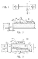
FIG. 1 schematically illustrates a non-continuous load termination ofIC devices - In
FIG. 1 , the distance from a to b is typically short. The value of the resistor R is chosen to match the line impedance and is typically about 45-80 ohms. The value of the capacitor C is chosen so that the RC time constant of the resistor R and the capacitor C in series is greater than the rise time of a signal and less than the total time of the signal pulse. Typical capacitance values are on the order of 30 picoFarads. - Conventional RC terminations are typically constructed of a surface mount technology (SMT) resistor and capacitor.
FIG. 2 is a cross section view of a portion of a printedcircuit board 25 having aSMT resistor 40 and aSMT capacitor 50 connected to anIC device 30 to form a conventional SMT RC transmission line termination for theIC 30. The signal line carrying the signal to theIC 30 is connected to acircuit trace 60 connecting theIC device 30 to theresistor 40. Thecapacitor 50 is coupled to acircuit trace 70 by one of a pair ofsolder pads 52 andsolder joints 58. Theresistor 40 is coupled to thecircuit trace 70 by asolder pad 42 and asolder joint 48. Thecapacitor 50 is coupled to avia hole 80 by theother solder pad 58 and acircuit trace 59. This arrangement places theresistor 40 and thecapacitor 50 in series with the signal line and connected to ground through a plated through-hole via 80. This conventional surface mount approach requires use of valuable surface real estate. Further, the requirement for solder joints reduces reliability and increases costs of fabrication. - Summary: According to a first embodiment, a capacitive/resistive device comprises a first electrode, a dielectric disposed over the first electrode, a resistor element formed on and adjacent to the dielectric, a conductive trace, and a second electrode disposed over the dielectric and in electrical contact with the resistor element. The capacitive/resistive device can be embedded in organic dielectric laminates, and incorporated in printed wiring boards.
- According to the above embodiment, both the resistor and the capacitor functions may be integrated into a single buried laminate, reducing the cost and difficulty in creating the resistor and capacitor functions. When the capacitive/resistive device is incorporated in a printed wiring board, embedding the capacitive/resistive device also frees up valuable real estate. Further, solder joints associated with SMT devices may be eliminated, thereby improving reliability. The capacitive/resistive device can be processed using conventional etching processes, further reducing production costs.
- Those skilled in the art will appreciate the above stated advantages and other advantages and benefits of various additional embodiments of the invention upon reading the following detailed description of the embodiments.
- BRIEF DESCRIPTION OF THE DRAWINGS: The detailed description will refer to the following drawings, wherein like numerals refer to like elements, and wherein:
-
FIG. 1 is a schematic illustration of a conventional (prior art) non-continuous load termination having a resistor and capacitor in series; -
FIG. 2 is a cross section view of a printed wiring board having a conventional (prior art) SMT RC transmission line termination for an integrated circuit device; -
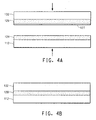
FIG. 3 is a section view of a portion of a printed wiring board having an embedded capacitive/resistive device according to a first embodiment; -
FIGS. 4A-4F illustrate a method of making the capacitive/resistive device illustrated inFIG. 3 . - Embodiments of the present invention are addressed to capacitive/resistive devices that may be buried in the substrate of a printed wiring board (PWB). Providing the capacitive and resistive functions within the PWB substrate conserves valuable surface real estate on the printed wiring board. The embodiments of the present invention also require fewer solder joints than conventional SMT termination arrangements.
-
FIG. 3 is a section view of a first embodiment of a portion of a printedwiring board 1000. The printedwiring board section 1000 includes an RC transmission line termination in which the resistor function and the capacitor function are integrated into a single capacitive/resistive device 100. Thedevice 100 is embedded within the printedwiring board section 1000. Thedevice 100 comprises abottom electrode 110, a dielectric 120, a top electrode ortop plate 130, aresistor element 140, and aconductive trace 145. Thedevice 100 provides a resistive and a capacitive function in a single laminate structure generally indicated by thebracket 101. - The
device 100 is coupled to anIC device 170 by a plated through hole via 150 extending throughdielectric layers conductive circuit trace 160. TheIC device 170 is connected to theconductive circuit trace 160 by asolder pad 172 and asolder joint 174. Other connection technology, however, may be used. Thebottom electrode 110 can also serve as a conductive ground plane in the printed wiring board, and can be coupled to aconductive circuit trace 111 that connects to other circuitry. -
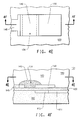
FIGS. 4A-4F illustrate a method of making a capacitor laminate including thedevice 100. -
FIG. 4A is a section view in front elevation of the first stage of manufacture in which first andsecond metal foils foils first foil 112, dried and cured, forming a firstdielectric layer 124. Curing may be performed by drying, for example, at 150°C, if the slurry is of a thermoplastic nature. Higher curing temperatures can be used if the slurry is a thermoset material. A similar seconddielectric layer 126 is formed in a similar manner on thesecond foil 132. - Solutions used to form the
dielectric layers - A thin
adhesive layer 127 may be applied to the surface of either one or both of thedielectric layers 124, 126 (shown inFIG. 4A on the dielectric layer 126). Theadhesive layer 127 may be formed from a thermoplastic polymer and may be filled with a high dielectric phase to avoid dilution of the dielectric constant. The two structures are then laminated together under heat and pressure in the direction shown by the arrows inFIG. 4A . - Referring to
FIG. 4B , lamination forms asingle dielectric 120 from thelayers adhesive layer 127 facilitates joining of thedielectric layers adhesive layer 127, however, may be dispensed with if thedielectric layers layers - An alternative method of forming the dielectric 120 may be to cast a filled or unfilled thermoplastic polymer onto one of the
foils dielectric layer 120 separately as a single film and laminating it to thefirst foil 112 and thesecond foil 132 using heat and pressure. - Unfilled polymers such as, for example, polyimide dielectric INTERRA™ HK 04 (available from DuPont Electronic Technologies, Wilmington, DE), can be used to form the dielectric 120.
- After lamination, a photoresist (not shown in
FIG. 4B ) is applied to thefoil 112 and thefoil 112 is imaged and etched, and the remaining photoresist is stripped using standard printing wiring board processing conditions.FIG. 4C is bottom section view of the resulting article after etching, taken online 4C-4C inFIG. 4D . Referring toFIG. 4C , the etching produces thebottom electrode 110 of thedevice 100. Theconductive circuit trace 111 can also be formed from thefoil 112 to connect thebottom electrode 110 to ground or other circuitry. -
FIG. 4D is a section view in front elevation taken online 4D-4D inFIG. 4C . Referring toFIG. 4D , thebottom electrode 110 side of the resulting article is laminated to adielectric laminate material 182. The lamination can be performed, for example, using FR4 prepreg, or other prepregs, in standard printing wiring board processes. - A photoresist (not shown in
FIG. 4D ) is applied to thefoil 132 and thefoil 132 is imaged and etched, and the remaining photoresist is stripped.FIG. 4E is top section view of the resulting article after etching, taken online 4E-4E inFIG. 4F. FIG. 4F is a section view in front elevation of the resulting article taken online 4F-4F inFIG. 4E . Referring toFIG. 4E , the etching produces thetop electrode 130 of thedevice 100, agap 134, and theconductive circuit trace 145. - Referring to
FIG. 4F , aresistor element 140 is formed by depositing a resistor material over the dielectric 120 and into thegap 134. Theresistor element 140 can be formed, for example, by depositing a polymer thick-film resistor paste, and curing the resistor paste. Thetop electrode 130 and theconductive circuit trace 145 serve as terminations for theresistor element 140. The polymer thick-film resistor paste can be made from materials such as, for example, carbon powders dispersed in a screen-printing vehicle. The screen-printing vehicle may comprise, for example, an epoxy resin dissolved in a suitable solvent. Other additives, such as surfactants, may be added to modify dielectric properties of theresultant resistor element 140. - After curing the
resistor element 140, adielectric layer 180 is laminated to the component side of thedielectric layer 182, forming alaminate structure 101. Thelaminate structure 101 resulting from the above process can then be incorporated into, for example, a printed wiring board as shown inFIG. 3 using conventional lamination and via formation processes. - Example 1 : This example of the
device 100 is discussed with reference toFIG. 3 . In this example, theelectrodes - The size (when viewed from a top plan perspective) of the capacitor needed for a transmission line termination of 30 picoFarad is 24.2 square mm, which corresponds to slightly less than 5 mm by 5 mm. The deposited resistor material is a screen-printable 100 ohm per square polymer thick-film resistor paste (available from DuPont Electronics).
- The size of the resistor in this example for a nominal 60 ohm resistance can be varied, preferably maintaining a length to width ratio in the range of about 0.6 to 1.0. The above capacitor size is acceptable if relatively few termination resistors are needed for the IC. In cases where large numbers of terminations are required, a laminate with a higher capacitance density is more desirable as the capacitor can be made smaller.
- Example 2: This example of the
device 100 is discussed with reference toFIG. 3 . In this example, a laminate is formed by casting a barium titanate-filled thermoplastic polyimide on one copper foil and laminating a second copper foil onto the surface of the barium titanate-filled thermoplastic polyimide coating. Barium titanate is advantageous as a filler as it is readily available and lead-free. - Lamination is performed at a suitable temperature and pressure so as to bond the articles together without use of a separate adhesive material. The
electrodes - The size of the capacitor needed for a transmission line termination as described above is 4.3 square mm, or approximately 2 mm by 2 mm. The deposited resistor is a screen printed 100 ohm per square inch polymer thick-film resistor paste (available from DuPont Electronics).
- A preferred size of the resistor in this example for a nominal 60 ohm resistance is 1.2 mm long and 2 mm wide, having a length to width aspect ratio 0.6 to 1.0.
- Example 3: This example of the
device 100 is discussed with reference toFIG. 3 . In this example, the laminate is made by casting a barium titanate-filled thermoplastic polyimide (available from DuPont Electronic Technologies) on two copper foils and laminating them together at a suitable temperature and pressure to bond them together. A separate adhesive material is not used. Theelectrodes dielectric 120 is a barium titanate-filled, polyimide dielectric of 8 microns thickness having a capacitance density of 6.2 nanoFarads per square inch. - The size of the capacitor needed for a transmission line termination as described above is 3.1 square mm, or approximately 1.77 mm by 1.77 mm. The deposited resistor can be formed from a screen printed 100 ohm per square polymer thick-film resistor paste (available from DuPont Electronics).
- A preferred size of the resistor for a nominal 60 ohm resistance in this example would be 1.06 mm long and 1.77 mm wide, having a length to width aspect ratio 0.6 to 1.0.
- According to the above embodiments, thin capacitor laminate structures in combination with resistors may be used to reduce the size of the buried capacitor function, and to more effectively bury RC transmission line terminations. Embedding the capacitor and resistor functions frees up valuable board surface real estate and eliminates solder joints associated with SMT devices, thereby improving reliability. Further, the laminates combining resistance and capacitance within the laminate can be processed using conventional etching processes, which reduces production costs.
- The above embodiments also provide other options for circuit designers and PWB fabricators. For example, one piece of laminate can be used to embed discrete resistors and discrete capacitors, which reduces the inductance associated with connecting resistors and capacitors.
- According to the above embodiments, thin capacitor laminate structures in combination with resistors may be used to reduce the size of the buried capacitor function, and to more effectively bury RC transmission line terminations. Embedding the capacitor and resistor functions frees up valuable board surface real estate and eliminates solder joints associated with SMT devices, thereby improving reliability. Further, the laminates combining resistance and capacitance within the laminate can be processed using conventional etching processes, which reduces production costs.
- The above embodiments also provides other options for circuit designers and PWB fabricators. For example, one piece of laminate can be used to embed many discrete resistors and many discrete capacitors, which reduces the inductance associated with connecting resistors and capacitors.
- The shapes of the capacitor embodiments in top plan view are generally rectangular. However, the capacitor electrodes, dielectrics, and other components and layers can have other regular or irregular surface area shapes, such as, for example, round, oblong, oval or polygonal shapes.
- A single capacitive/
resistive device 100 is formed in thelaminate structures 101 described above. However, panel structures and printed wiring boards can include a large number of individual capacitive/resistive devices of differing type and arrangement. - In the above embodiment, resistance, capacitance and inductance combine to create a specific circuit impedance, typically identified by the capital letter Z. The resistance and capacitance may be structured to achieve a specific impedance. Changing the resistance, capacitance, or both will change the inductance. All three changes can be controlled to define the final impedance. In other words, the impedance of the laminate is 'tunable.'
- The foregoing description of the invention illustrates and describes the present invention. Additionally, the disclosure shows and describes only selected preferred embodiments of the invention, but it is to be understood that the invention is capable of use in various other combinations, modifications, and environments and is capable of changes or modifications within the scope of the inventive concept as expressed herein, commensurate with the above teachings, and/or within the skill or knowledge of the relevant art.
- The embodiments described hereinabove are further intended to explain best modes known of practicing the invention and to enable others skilled in the art to utilize the invention in such, or other, embodiments and with the various modifications required by the particular applications or uses of the invention. Accordingly, the description is not intended to limit the invention to the form disclosed herein. Also, it is intended that the appended claims be construed to include alternative embodiments, not explicitly defined in the detailed description.
Claims (7)
- A capacitive/resistive device, comprising:a first electrode;a dielectric disposed over the first electrode;a resistor element formed on and adjacent to the dielectric;a conductive trace; anda second electrode disposed over the dielectric and in electrical contact with the resistor element, wherein the dielectric is disposed between the first electrode and the second electrode.
- The capacitive/resistive device of claim 1, wherein the resistor element extends between and partially covers the second electrode and said conductive trace.
- The capacitive/resistive device of claim 2, wherein the resistor element extends across a gap between the second electrode and the conductive trace and abuts the dielectric.
- The capacitive/resistive device of claim 1, wherein the dielectric comprises an unfilled polymer.
- The capacitive/resistive device of claim 1, wherein the dielectric comprises a polymer filled with a dielectric functional phase.
- The capacitive/resistive device of claim 1 embedded within at least two organic dielectric laminate layers, wherein the laminate layers and the capacitive/resistive device form a laminate structure.
- A printed wiring board, comprising:at least one laminate structure according to claim 6; andat least one IC device disposed on a top surface of the printed wiring board, wherein the IC device is electrically coupled to the capacitive/resistive device.
Applications Claiming Priority (2)
| Application Number | Priority Date | Filing Date | Title |
|---|---|---|---|
| US10/967,569 US7436678B2 (en) | 2004-10-18 | 2004-10-18 | Capacitive/resistive devices and printed wiring boards incorporating such devices and methods of making thereof |
| EP05020897A EP1648208B1 (en) | 2004-10-18 | 2005-09-26 | Capacitive/resistive devices and printed wiring boards incorporating such devices, and methods of making thereof |
Related Parent Applications (1)
| Application Number | Title | Priority Date | Filing Date |
|---|---|---|---|
| EP05020897A Division EP1648208B1 (en) | 2004-10-18 | 2005-09-26 | Capacitive/resistive devices and printed wiring boards incorporating such devices, and methods of making thereof |
Publications (1)
| Publication Number | Publication Date |
|---|---|
| EP2104407A1 true EP2104407A1 (en) | 2009-09-23 |
Family
ID=35586143
Family Applications (2)
| Application Number | Title | Priority Date | Filing Date |
|---|---|---|---|
| EP09007939A Withdrawn EP2104407A1 (en) | 2004-10-18 | 2005-09-26 | Capacitive/resistive devices and printed wiring boards incorporating such devices, and methods of making thereof |
| EP05020897A Active EP1648208B1 (en) | 2004-10-18 | 2005-09-26 | Capacitive/resistive devices and printed wiring boards incorporating such devices, and methods of making thereof |
Family Applications After (1)
| Application Number | Title | Priority Date | Filing Date |
|---|---|---|---|
| EP05020897A Active EP1648208B1 (en) | 2004-10-18 | 2005-09-26 | Capacitive/resistive devices and printed wiring boards incorporating such devices, and methods of making thereof |
Country Status (7)
| Country | Link |
|---|---|
| US (2) | US7436678B2 (en) |
| EP (2) | EP2104407A1 (en) |
| JP (1) | JP2006121088A (en) |
| KR (1) | KR100812515B1 (en) |
| CN (1) | CN1783378A (en) |
| DE (1) | DE602005015657D1 (en) |
| TW (2) | TWI412306B (en) |
Cited By (28)
| Publication number | Priority date | Publication date | Assignee | Title |
|---|---|---|---|---|
| US9554477B1 (en) | 2015-12-18 | 2017-01-24 | International Business Machines Corporation | Tamper-respondent assemblies with enclosure-to-board protection |
| US9555606B1 (en) | 2015-12-09 | 2017-01-31 | International Business Machines Corporation | Applying pressure to adhesive using CTE mismatch between components |
| US9560737B2 (en) | 2015-03-04 | 2017-01-31 | International Business Machines Corporation | Electronic package with heat transfer element(s) |
| US9578764B1 (en) | 2015-09-25 | 2017-02-21 | International Business Machines Corporation | Enclosure with inner tamper-respondent sensor(s) and physical security element(s) |
| US9591776B1 (en) | 2015-09-25 | 2017-03-07 | International Business Machines Corporation | Enclosure with inner tamper-respondent sensor(s) |
| US9858776B1 (en) | 2016-06-28 | 2018-01-02 | International Business Machines Corporation | Tamper-respondent assembly with nonlinearity monitoring |
| US9881880B2 (en) | 2016-05-13 | 2018-01-30 | International Business Machines Corporation | Tamper-proof electronic packages with stressed glass component substrate(s) |
| US9894749B2 (en) | 2015-09-25 | 2018-02-13 | International Business Machines Corporation | Tamper-respondent assemblies with bond protection |
| US9904811B2 (en) | 2016-04-27 | 2018-02-27 | International Business Machines Corporation | Tamper-proof electronic packages with two-phase dielectric fluid |
| US9911012B2 (en) | 2015-09-25 | 2018-03-06 | International Business Machines Corporation | Overlapping, discrete tamper-respondent sensors |
| US9913370B2 (en) | 2016-05-13 | 2018-03-06 | International Business Machines Corporation | Tamper-proof electronic packages formed with stressed glass |
| US9913389B2 (en) | 2015-12-01 | 2018-03-06 | International Business Corporation Corporation | Tamper-respondent assembly with vent structure |
| US9916744B2 (en) | 2016-02-25 | 2018-03-13 | International Business Machines Corporation | Multi-layer stack with embedded tamper-detect protection |
| US9924591B2 (en) | 2015-09-25 | 2018-03-20 | International Business Machines Corporation | Tamper-respondent assemblies |
| US9978231B2 (en) | 2015-10-21 | 2018-05-22 | International Business Machines Corporation | Tamper-respondent assembly with protective wrap(s) over tamper-respondent sensor(s) |
| US9999124B2 (en) | 2016-11-02 | 2018-06-12 | International Business Machines Corporation | Tamper-respondent assemblies with trace regions of increased susceptibility to breaking |
| US10098235B2 (en) | 2015-09-25 | 2018-10-09 | International Business Machines Corporation | Tamper-respondent assemblies with region(s) of increased susceptibility to damage |
| US10136519B2 (en) | 2015-10-19 | 2018-11-20 | International Business Machines Corporation | Circuit layouts of tamper-respondent sensors |
| US10172239B2 (en) | 2015-09-25 | 2019-01-01 | International Business Machines Corporation | Tamper-respondent sensors with formed flexible layer(s) |
| US10168185B2 (en) | 2015-09-25 | 2019-01-01 | International Business Machines Corporation | Circuit boards and electronic packages with embedded tamper-respondent sensor |
| US10271424B2 (en) | 2016-09-26 | 2019-04-23 | International Business Machines Corporation | Tamper-respondent assemblies with in situ vent structure(s) |
| US10299372B2 (en) | 2016-09-26 | 2019-05-21 | International Business Machines Corporation | Vented tamper-respondent assemblies |
| US10306753B1 (en) | 2018-02-22 | 2019-05-28 | International Business Machines Corporation | Enclosure-to-board interface with tamper-detect circuit(s) |
| US10321589B2 (en) | 2016-09-19 | 2019-06-11 | International Business Machines Corporation | Tamper-respondent assembly with sensor connection adapter |
| US10327343B2 (en) | 2015-12-09 | 2019-06-18 | International Business Machines Corporation | Applying pressure to adhesive using CTE mismatch between components |
| US10327329B2 (en) | 2017-02-13 | 2019-06-18 | International Business Machines Corporation | Tamper-respondent assembly with flexible tamper-detect sensor(s) overlying in-situ-formed tamper-detect sensor |
| US10426037B2 (en) | 2015-07-15 | 2019-09-24 | International Business Machines Corporation | Circuitized structure with 3-dimensional configuration |
| US11122682B2 (en) | 2018-04-04 | 2021-09-14 | International Business Machines Corporation | Tamper-respondent sensors with liquid crystal polymer layers |
Families Citing this family (16)
| Publication number | Priority date | Publication date | Assignee | Title |
|---|---|---|---|---|
| DE102004020172A1 (en) * | 2004-04-24 | 2005-11-24 | Robert Bosch Gmbh | Monolithic controller for the generator unit of a motor vehicle |
| US7235745B2 (en) * | 2005-01-10 | 2007-06-26 | Endicott Interconnect Technologies, Inc. | Resistor material with metal component for use in circuitized substrates, circuitized substrate utilizing same, method of making said ciruitized substrate, and information handling system utilizing said ciruitized substrate |
| US20060286696A1 (en) * | 2005-06-21 | 2006-12-21 | Peiffer Joel S | Passive electrical article |
| KR100826352B1 (en) * | 2007-01-30 | 2008-05-02 | 삼성전기주식회사 | Embedded capacitor printed circuit board |
| EP2034808A3 (en) * | 2007-08-07 | 2011-04-06 | Delphi Technologies, Inc. | Embedded resistor and capacitor circuit and method of fabricating same |
| CN101661920B (en) * | 2008-08-26 | 2011-06-29 | 欣兴电子股份有限公司 | Chip packaging carrying plate and making method thereof |
| JP5995860B2 (en) * | 2010-12-06 | 2016-09-21 | スリーエム イノベイティブ プロパティズ カンパニー | Composite diode, electronic device and manufacturing method thereof |
| CN103247860B (en) * | 2012-02-09 | 2017-08-25 | 深圳光启创新技术有限公司 | The preparation method and Meta Materials of a kind of Meta Materials |
| CN105047411A (en) * | 2015-08-12 | 2015-11-11 | 深圳市槟城电子有限公司 | Module with interconnected resistor and capacitor and fabrication method thereof |
| CN105047642B (en) * | 2015-08-12 | 2024-01-19 | 深圳市槟城电子股份有限公司 | Port protection circuit integrated package |
| US10083781B2 (en) | 2015-10-30 | 2018-09-25 | Vishay Dale Electronics, Llc | Surface mount resistors and methods of manufacturing same |
| CN107340900B (en) * | 2016-04-29 | 2020-09-18 | 北京小米移动软件有限公司 | Mobile terminal middle frame and mobile terminal |
| CN110140203A (en) * | 2016-11-18 | 2019-08-16 | 哈钦森技术股份有限公司 | High aspect ratio electroplated structural and anisotropy electroplating technology |
| US10438729B2 (en) | 2017-11-10 | 2019-10-08 | Vishay Dale Electronics, Llc | Resistor with upper surface heat dissipation |
| DE102018127428B3 (en) * | 2018-11-02 | 2020-02-20 | Johnson Electric Germany GmbH & Co. KG | Diagnostic switch, in particular diagnostic micro signal switch and method for its manufacture |
| US20210345481A1 (en) * | 2020-04-29 | 2021-11-04 | Qualcomm Incorporated | Integral super-capacitor for low power applications |
Citations (6)
| Publication number | Priority date | Publication date | Assignee | Title |
|---|---|---|---|---|
| US4410867A (en) * | 1978-12-28 | 1983-10-18 | Western Electric Company, Inc. | Alpha tantalum thin film circuit device |
| US4496435A (en) * | 1983-02-08 | 1985-01-29 | Nec Corporation | Method of manufacturing thin film circuits |
| US5172304A (en) * | 1990-11-22 | 1992-12-15 | Murata Manufacturing Co., Ltd. | Capacitor-containing wiring board and method of manufacturing the same |
| US5731747A (en) * | 1995-02-27 | 1998-03-24 | U.S. Philips Corporation | Electronic component having a thin-film structure with passive elements |
| US6278356B1 (en) * | 2000-05-17 | 2001-08-21 | Compeq Manufacturing Company Limited | Flat, built-in resistors and capacitors for a printed circuit board |
| US20040144476A1 (en) * | 2003-01-09 | 2004-07-29 | Junzo Fukuta | Method of producing ceramic multilayer substrate |
Family Cites Families (30)
| Publication number | Priority date | Publication date | Assignee | Title |
|---|---|---|---|---|
| US3934119A (en) | 1974-09-17 | 1976-01-20 | Texas Instruments Incorporated | Electrical resistance heaters |
| US4093036A (en) * | 1976-09-07 | 1978-06-06 | Knutson Glenn C | Irrigation tower drive |
| US4377652A (en) | 1978-02-17 | 1983-03-22 | Asahi Kasei Kogyo Kabushiki Kaisha | Polyamide-imide compositions and articles for electrical use prepared therefrom |
| US4399417A (en) * | 1980-06-06 | 1983-08-16 | Bell Telephone Laboratories, Incorporated | Integrated CRC filter circuit |
| US4407883A (en) | 1982-03-03 | 1983-10-04 | Uop Inc. | Laminates for printed circuit boards |
| JPS58190091A (en) | 1982-04-30 | 1983-11-05 | 宇部興産株式会社 | Method of producing flexible circuit board |
| JPS60113993A (en) * | 1983-11-25 | 1985-06-20 | 三菱電機株式会社 | Method of producing multilayer circuit board |
| JPS63278399A (en) * | 1987-05-11 | 1988-11-16 | Japan Radio Co Ltd | Composing method for mixed thick film circuit |
| US5093036A (en) | 1988-09-20 | 1992-03-03 | Raychem Corporation | Conductive polymer composition |
| JPH03125416A (en) * | 1989-10-09 | 1991-05-28 | Nippon Oil & Fats Co Ltd | Circuit board |
| JPH0565456A (en) | 1991-09-09 | 1993-03-19 | Sumitomo Bakelite Co Ltd | Resin paste for airtight sealing |
| JPH05152111A (en) * | 1991-11-28 | 1993-06-18 | Rohm Co Ltd | Chip-shaped composite component |
| EP0588136B1 (en) | 1992-09-15 | 1996-11-13 | E.I. Du Pont De Nemours And Company | Polymer thick film resistor compositions |
| US6111005A (en) | 1993-07-30 | 2000-08-29 | Diemat, Inc. | Polymeric adhesive paste |
| US6140402A (en) | 1993-07-30 | 2000-10-31 | Diemat, Inc. | Polymeric adhesive paste |
| JP3117175B2 (en) | 1994-02-09 | 2000-12-11 | アルプス電気株式会社 | Resistor |
| TW301843B (en) | 1994-11-15 | 1997-04-01 | Ibm | Electrically conductive paste and composite and their use as an electrically conductive connector |
| JPH08306503A (en) * | 1995-05-11 | 1996-11-22 | Rohm Co Ltd | Chip-like electronic part |
| JPH0992983A (en) * | 1995-07-17 | 1997-04-04 | Sumitomo Kinzoku Electro Device:Kk | Manufacture of ceramic multilayer board |
| US5699224A (en) * | 1995-10-25 | 1997-12-16 | Rohm Co., Ltd. | Thick-film capacitor and chip-type composite electronic component utilizing the same |
| US5993698A (en) | 1997-11-06 | 1999-11-30 | Acheson Industries, Inc. | Electrical device containing positive temperature coefficient resistor composition and method of manufacturing the device |
| JP3890712B2 (en) * | 1997-11-18 | 2007-03-07 | ソニー株式会社 | Multilayer wiring board and manufacturing method thereof |
| JP4297617B2 (en) * | 1999-03-17 | 2009-07-15 | モトローラ・インコーポレイテッド | How to make a resistor |
| US6030553A (en) | 1999-04-01 | 2000-02-29 | Industrial Technology Research Institute | Polymer thick film resistor pastes |
| US6535398B1 (en) * | 2000-03-07 | 2003-03-18 | Fujitsu Limited | Multichip module substrates with buried discrete capacitors and components and methods for making |
| US6541137B1 (en) | 2000-07-31 | 2003-04-01 | Motorola, Inc. | Multi-layer conductor-dielectric oxide structure |
| JP2002252297A (en) * | 2001-02-23 | 2002-09-06 | Hitachi Ltd | Electronic circuit device using multilayer circuit board |
| JP4047669B2 (en) * | 2002-06-14 | 2008-02-13 | クローバー電子工業株式会社 | Manufacturing method of multilayer printed wiring board |
| US6910264B2 (en) | 2003-01-03 | 2005-06-28 | Phoenix Precision Technology Corp. | Method for making a multilayer circuit board having embedded passive components |
| JP4449772B2 (en) * | 2004-04-09 | 2010-04-14 | 株式会社デンソー | Power semiconductor switching element and semiconductor power module using the same |
-
2004
- 2004-10-18 US US10/967,569 patent/US7436678B2/en active Active
-
2005
- 2005-09-26 EP EP09007939A patent/EP2104407A1/en not_active Withdrawn
- 2005-09-26 EP EP05020897A patent/EP1648208B1/en active Active
- 2005-09-26 DE DE602005015657T patent/DE602005015657D1/en active Active
- 2005-10-04 TW TW094134607A patent/TWI412306B/en active
- 2005-10-04 TW TW102121911A patent/TW201343017A/en unknown
- 2005-10-17 KR KR1020050097354A patent/KR100812515B1/en active IP Right Grant
- 2005-10-18 CN CNA2005101161073A patent/CN1783378A/en active Pending
- 2005-10-18 JP JP2005303552A patent/JP2006121088A/en active Pending
-
2007
- 2007-01-26 US US11/698,423 patent/US7571536B2/en active Active
Patent Citations (6)
| Publication number | Priority date | Publication date | Assignee | Title |
|---|---|---|---|---|
| US4410867A (en) * | 1978-12-28 | 1983-10-18 | Western Electric Company, Inc. | Alpha tantalum thin film circuit device |
| US4496435A (en) * | 1983-02-08 | 1985-01-29 | Nec Corporation | Method of manufacturing thin film circuits |
| US5172304A (en) * | 1990-11-22 | 1992-12-15 | Murata Manufacturing Co., Ltd. | Capacitor-containing wiring board and method of manufacturing the same |
| US5731747A (en) * | 1995-02-27 | 1998-03-24 | U.S. Philips Corporation | Electronic component having a thin-film structure with passive elements |
| US6278356B1 (en) * | 2000-05-17 | 2001-08-21 | Compeq Manufacturing Company Limited | Flat, built-in resistors and capacitors for a printed circuit board |
| US20040144476A1 (en) * | 2003-01-09 | 2004-07-29 | Junzo Fukuta | Method of producing ceramic multilayer substrate |
Cited By (64)
| Publication number | Priority date | Publication date | Assignee | Title |
|---|---|---|---|---|
| US10237964B2 (en) | 2015-03-04 | 2019-03-19 | International Business Machines Corporation | Manufacturing electronic package with heat transfer element(s) |
| US9560737B2 (en) | 2015-03-04 | 2017-01-31 | International Business Machines Corporation | Electronic package with heat transfer element(s) |
| US10524362B2 (en) | 2015-07-15 | 2019-12-31 | International Business Machines Corporation | Circuitized structure with 3-dimensional configuration |
| US10426037B2 (en) | 2015-07-15 | 2019-09-24 | International Business Machines Corporation | Circuitized structure with 3-dimensional configuration |
| US10178818B2 (en) | 2015-09-25 | 2019-01-08 | International Business Machines Corporation | Enclosure with inner tamper-respondent sensor(s) and physical security element(s) |
| US9936573B2 (en) | 2015-09-25 | 2018-04-03 | International Business Machines Corporation | Tamper-respondent assemblies |
| US9717154B2 (en) | 2015-09-25 | 2017-07-25 | International Business Machines Corporation | Enclosure with inner tamper-respondent sensor(s) |
| US10175064B2 (en) | 2015-09-25 | 2019-01-08 | International Business Machines Corporation | Circuit boards and electronic packages with embedded tamper-respondent sensor |
| US10624202B2 (en) | 2015-09-25 | 2020-04-14 | International Business Machines Corporation | Tamper-respondent assemblies with bond protection |
| US10257939B2 (en) | 2015-09-25 | 2019-04-09 | International Business Machines Corporation | Method of fabricating tamper-respondent sensor |
| US9894749B2 (en) | 2015-09-25 | 2018-02-13 | International Business Machines Corporation | Tamper-respondent assemblies with bond protection |
| US9578764B1 (en) | 2015-09-25 | 2017-02-21 | International Business Machines Corporation | Enclosure with inner tamper-respondent sensor(s) and physical security element(s) |
| US9911012B2 (en) | 2015-09-25 | 2018-03-06 | International Business Machines Corporation | Overlapping, discrete tamper-respondent sensors |
| US10395067B2 (en) | 2015-09-25 | 2019-08-27 | International Business Machines Corporation | Method of fabricating a tamper-respondent sensor assembly |
| US10685146B2 (en) | 2015-09-25 | 2020-06-16 | International Business Machines Corporation | Overlapping, discrete tamper-respondent sensors |
| US9913416B2 (en) | 2015-09-25 | 2018-03-06 | International Business Machines Corporation | Enclosure with inner tamper-respondent sensor(s) and physical security element(s) |
| US9913362B2 (en) | 2015-09-25 | 2018-03-06 | International Business Machines Corporation | Tamper-respondent assemblies with bond protection |
| US10378925B2 (en) | 2015-09-25 | 2019-08-13 | International Business Machines Corporation | Circuit boards and electronic packages with embedded tamper-respondent sensor |
| US9924591B2 (en) | 2015-09-25 | 2018-03-20 | International Business Machines Corporation | Tamper-respondent assemblies |
| US9591776B1 (en) | 2015-09-25 | 2017-03-07 | International Business Machines Corporation | Enclosure with inner tamper-respondent sensor(s) |
| US10264665B2 (en) | 2015-09-25 | 2019-04-16 | International Business Machines Corporation | Tamper-respondent assemblies with bond protection |
| US10378924B2 (en) | 2015-09-25 | 2019-08-13 | International Business Machines Corporation | Circuit boards and electronic packages with embedded tamper-respondent sensor |
| US10098235B2 (en) | 2015-09-25 | 2018-10-09 | International Business Machines Corporation | Tamper-respondent assemblies with region(s) of increased susceptibility to damage |
| US10331915B2 (en) | 2015-09-25 | 2019-06-25 | International Business Machines Corporation | Overlapping, discrete tamper-respondent sensors |
| US10271434B2 (en) | 2015-09-25 | 2019-04-23 | International Business Machines Corporation | Method of fabricating a tamper-respondent assembly with region(s) of increased susceptibility to damage |
| US10168185B2 (en) | 2015-09-25 | 2019-01-01 | International Business Machines Corporation | Circuit boards and electronic packages with embedded tamper-respondent sensor |
| US10172239B2 (en) | 2015-09-25 | 2019-01-01 | International Business Machines Corporation | Tamper-respondent sensors with formed flexible layer(s) |
| US10334722B2 (en) | 2015-09-25 | 2019-06-25 | International Business Machines Corporation | Tamper-respondent assemblies |
| US10143090B2 (en) | 2015-10-19 | 2018-11-27 | International Business Machines Corporation | Circuit layouts of tamper-respondent sensors |
| US10136519B2 (en) | 2015-10-19 | 2018-11-20 | International Business Machines Corporation | Circuit layouts of tamper-respondent sensors |
| US9978231B2 (en) | 2015-10-21 | 2018-05-22 | International Business Machines Corporation | Tamper-respondent assembly with protective wrap(s) over tamper-respondent sensor(s) |
| US9913389B2 (en) | 2015-12-01 | 2018-03-06 | International Business Corporation Corporation | Tamper-respondent assembly with vent structure |
| US10251288B2 (en) | 2015-12-01 | 2019-04-02 | International Business Machines Corporation | Tamper-respondent assembly with vent structure |
| US10327343B2 (en) | 2015-12-09 | 2019-06-18 | International Business Machines Corporation | Applying pressure to adhesive using CTE mismatch between components |
| US9555606B1 (en) | 2015-12-09 | 2017-01-31 | International Business Machines Corporation | Applying pressure to adhesive using CTE mismatch between components |
| US9877383B2 (en) | 2015-12-18 | 2018-01-23 | International Business Machines Corporation | Tamper-respondent assemblies with enclosure-to-board protection |
| US9661747B1 (en) | 2015-12-18 | 2017-05-23 | International Business Machines Corporation | Tamper-respondent assemblies with enclosure-to-board protection |
| US9554477B1 (en) | 2015-12-18 | 2017-01-24 | International Business Machines Corporation | Tamper-respondent assemblies with enclosure-to-board protection |
| US10172232B2 (en) | 2015-12-18 | 2019-01-01 | International Business Machines Corporation | Tamper-respondent assemblies with enclosure-to-board protection |
| US10115275B2 (en) | 2016-02-25 | 2018-10-30 | International Business Machines Corporation | Multi-layer stack with embedded tamper-detect protection |
| US9916744B2 (en) | 2016-02-25 | 2018-03-13 | International Business Machines Corporation | Multi-layer stack with embedded tamper-detect protection |
| US10169967B1 (en) | 2016-02-25 | 2019-01-01 | International Business Machines Corporation | Multi-layer stack with embedded tamper-detect protection |
| US10217336B2 (en) | 2016-02-25 | 2019-02-26 | International Business Machines Corporation | Multi-layer stack with embedded tamper-detect protection |
| US10169968B1 (en) | 2016-02-25 | 2019-01-01 | International Business Machines Corporation | Multi-layer stack with embedded tamper-detect protection |
| US10169624B2 (en) | 2016-04-27 | 2019-01-01 | International Business Machines Corporation | Tamper-proof electronic packages with two-phase dielectric fluid |
| US9904811B2 (en) | 2016-04-27 | 2018-02-27 | International Business Machines Corporation | Tamper-proof electronic packages with two-phase dielectric fluid |
| US10535619B2 (en) | 2016-05-13 | 2020-01-14 | International Business Machines Corporation | Tamper-proof electronic packages with stressed glass component substrate(s) |
| US9913370B2 (en) | 2016-05-13 | 2018-03-06 | International Business Machines Corporation | Tamper-proof electronic packages formed with stressed glass |
| US10257924B2 (en) | 2016-05-13 | 2019-04-09 | International Business Machines Corporation | Tamper-proof electronic packages formed with stressed glass |
| US10535618B2 (en) | 2016-05-13 | 2020-01-14 | International Business Machines Corporation | Tamper-proof electronic packages with stressed glass component substrate(s) |
| US9881880B2 (en) | 2016-05-13 | 2018-01-30 | International Business Machines Corporation | Tamper-proof electronic packages with stressed glass component substrate(s) |
| US10177102B2 (en) | 2016-05-13 | 2019-01-08 | International Business Machines Corporation | Tamper-proof electronic packages with stressed glass component substrate(s) |
| US10242543B2 (en) | 2016-06-28 | 2019-03-26 | International Business Machines Corporation | Tamper-respondent assembly with nonlinearity monitoring |
| US9858776B1 (en) | 2016-06-28 | 2018-01-02 | International Business Machines Corporation | Tamper-respondent assembly with nonlinearity monitoring |
| US10321589B2 (en) | 2016-09-19 | 2019-06-11 | International Business Machines Corporation | Tamper-respondent assembly with sensor connection adapter |
| US10271424B2 (en) | 2016-09-26 | 2019-04-23 | International Business Machines Corporation | Tamper-respondent assemblies with in situ vent structure(s) |
| US10299372B2 (en) | 2016-09-26 | 2019-05-21 | International Business Machines Corporation | Vented tamper-respondent assemblies |
| US10667389B2 (en) | 2016-09-26 | 2020-05-26 | International Business Machines Corporation | Vented tamper-respondent assemblies |
| US9999124B2 (en) | 2016-11-02 | 2018-06-12 | International Business Machines Corporation | Tamper-respondent assemblies with trace regions of increased susceptibility to breaking |
| US10327329B2 (en) | 2017-02-13 | 2019-06-18 | International Business Machines Corporation | Tamper-respondent assembly with flexible tamper-detect sensor(s) overlying in-situ-formed tamper-detect sensor |
| US10531561B2 (en) | 2018-02-22 | 2020-01-07 | International Business Machines Corporation | Enclosure-to-board interface with tamper-detect circuit(s) |
| US10306753B1 (en) | 2018-02-22 | 2019-05-28 | International Business Machines Corporation | Enclosure-to-board interface with tamper-detect circuit(s) |
| US11083082B2 (en) | 2018-02-22 | 2021-08-03 | International Business Machines Corporation | Enclosure-to-board interface with tamper-detect circuit(s) |
| US11122682B2 (en) | 2018-04-04 | 2021-09-14 | International Business Machines Corporation | Tamper-respondent sensors with liquid crystal polymer layers |
Also Published As
| Publication number | Publication date |
|---|---|
| KR20060054033A (en) | 2006-05-22 |
| TW201343017A (en) | 2013-10-16 |
| TWI412306B (en) | 2013-10-11 |
| KR100812515B1 (en) | 2008-03-11 |
| US7571536B2 (en) | 2009-08-11 |
| US20060082981A1 (en) | 2006-04-20 |
| US7436678B2 (en) | 2008-10-14 |
| DE602005015657D1 (en) | 2009-09-10 |
| TW200628024A (en) | 2006-08-01 |
| CN1783378A (en) | 2006-06-07 |
| EP1648208B1 (en) | 2009-07-29 |
| JP2006121088A (en) | 2006-05-11 |
| EP1648208A1 (en) | 2006-04-19 |
| US20070139901A1 (en) | 2007-06-21 |
Similar Documents
| Publication | Publication Date | Title |
|---|---|---|
| EP1648208B1 (en) | Capacitive/resistive devices and printed wiring boards incorporating such devices, and methods of making thereof | |
| EP1648207B1 (en) | Capacitive/Resistive devices, high dielectric constant organic dielectric laminates and printed wiring boards incorporating such devices, and methods of making thereof | |
| EP1675131B1 (en) | Capacitive devices, organic dielectric laminates and printed wiring boards incorporating such devices, and methods of making thereof | |
| US7813141B2 (en) | Capacitive/resistive devices, organic dielectric laminates and printed wiring boards incorporating such devices, and methods of making thereof | |
| KR101401863B1 (en) | Printed Circuit Board With Embeded Capacitor And Fabricating Method Thereof | |
| US20070006435A1 (en) | Capacitive devices, organic dielectric laminates, multilayer structures incorporating such devices, and methods of making thereof | |
| EP1675449A1 (en) | Devices comprising a power core and methods of making thereof | |
| JP4207517B2 (en) | Embedded substrate | |
| JPH1056251A (en) | Printed board with built-in electronic component and its production | |
| JP4269657B2 (en) | Dielectric multilayer sheet, capacitor sheet with built-in substrate, and substrate with built-in element |
Legal Events
| Date | Code | Title | Description |
|---|---|---|---|
| PUAI | Public reference made under article 153(3) epc to a published international application that has entered the european phase |
Free format text: ORIGINAL CODE: 0009012 |
|
| AC | Divisional application: reference to earlier application |
Ref document number: 1648208 Country of ref document: EP Kind code of ref document: P |
|
| AK | Designated contracting states |
Kind code of ref document: A1 Designated state(s): DE FR GB |
|
| STAA | Information on the status of an ep patent application or granted ep patent |
Free format text: STATUS: THE APPLICATION IS DEEMED TO BE WITHDRAWN |
|
| 18D | Application deemed to be withdrawn |
Effective date: 20100324 |