JP2006121088A - Capacitive resistance device, printed circuit board incorporated with such device, and method of manufacturing the same - Google Patents
Capacitive resistance device, printed circuit board incorporated with such device, and method of manufacturing the same Download PDFInfo
- Publication number
- JP2006121088A JP2006121088A JP2005303552A JP2005303552A JP2006121088A JP 2006121088 A JP2006121088 A JP 2006121088A JP 2005303552 A JP2005303552 A JP 2005303552A JP 2005303552 A JP2005303552 A JP 2005303552A JP 2006121088 A JP2006121088 A JP 2006121088A
- Authority
- JP
- Japan
- Prior art keywords
- dielectric
- electrode
- capacitive
- resistive
- metal foil
- Prior art date
- Legal status (The legal status is an assumption and is not a legal conclusion. Google has not performed a legal analysis and makes no representation as to the accuracy of the status listed.)
- Pending
Links
Images


Classifications
-
- H—ELECTRICITY
- H01—ELECTRIC ELEMENTS
- H01L—SEMICONDUCTOR DEVICES NOT COVERED BY CLASS H10
- H01L27/00—Devices consisting of a plurality of semiconductor or other solid-state components formed in or on a common substrate
- H01L27/02—Devices consisting of a plurality of semiconductor or other solid-state components formed in or on a common substrate including semiconductor components specially adapted for rectifying, oscillating, amplifying or switching and having at least one potential-jump barrier or surface barrier; including integrated passive circuit elements with at least one potential-jump barrier or surface barrier
- H01L27/04—Devices consisting of a plurality of semiconductor or other solid-state components formed in or on a common substrate including semiconductor components specially adapted for rectifying, oscillating, amplifying or switching and having at least one potential-jump barrier or surface barrier; including integrated passive circuit elements with at least one potential-jump barrier or surface barrier the substrate being a semiconductor body
-
- H—ELECTRICITY
- H05—ELECTRIC TECHNIQUES NOT OTHERWISE PROVIDED FOR
- H05K—PRINTED CIRCUITS; CASINGS OR CONSTRUCTIONAL DETAILS OF ELECTRIC APPARATUS; MANUFACTURE OF ASSEMBLAGES OF ELECTRICAL COMPONENTS
- H05K1/00—Printed circuits
- H05K1/16—Printed circuits incorporating printed electric components, e.g. printed resistor, capacitor, inductor
- H05K1/167—Printed circuits incorporating printed electric components, e.g. printed resistor, capacitor, inductor incorporating printed resistors
-
- H—ELECTRICITY
- H05—ELECTRIC TECHNIQUES NOT OTHERWISE PROVIDED FOR
- H05K—PRINTED CIRCUITS; CASINGS OR CONSTRUCTIONAL DETAILS OF ELECTRIC APPARATUS; MANUFACTURE OF ASSEMBLAGES OF ELECTRICAL COMPONENTS
- H05K1/00—Printed circuits
- H05K1/16—Printed circuits incorporating printed electric components, e.g. printed resistor, capacitor, inductor
- H05K1/162—Printed circuits incorporating printed electric components, e.g. printed resistor, capacitor, inductor incorporating printed capacitors
-
- H—ELECTRICITY
- H01—ELECTRIC ELEMENTS
- H01L—SEMICONDUCTOR DEVICES NOT COVERED BY CLASS H10
- H01L2924/00—Indexing scheme for arrangements or methods for connecting or disconnecting semiconductor or solid-state bodies as covered by H01L24/00
- H01L2924/19—Details of hybrid assemblies other than the semiconductor or other solid state devices to be connected
- H01L2924/191—Disposition
- H01L2924/19101—Disposition of discrete passive components
- H01L2924/19105—Disposition of discrete passive components in a side-by-side arrangement on a common die mounting substrate
-
- H—ELECTRICITY
- H05—ELECTRIC TECHNIQUES NOT OTHERWISE PROVIDED FOR
- H05K—PRINTED CIRCUITS; CASINGS OR CONSTRUCTIONAL DETAILS OF ELECTRIC APPARATUS; MANUFACTURE OF ASSEMBLAGES OF ELECTRICAL COMPONENTS
- H05K2201/00—Indexing scheme relating to printed circuits covered by H05K1/00
- H05K2201/03—Conductive materials
- H05K2201/0332—Structure of the conductor
- H05K2201/0335—Layered conductors or foils
- H05K2201/0355—Metal foils
-
- H—ELECTRICITY
- H05—ELECTRIC TECHNIQUES NOT OTHERWISE PROVIDED FOR
- H05K—PRINTED CIRCUITS; CASINGS OR CONSTRUCTIONAL DETAILS OF ELECTRIC APPARATUS; MANUFACTURE OF ASSEMBLAGES OF ELECTRICAL COMPONENTS
- H05K2201/00—Indexing scheme relating to printed circuits covered by H05K1/00
- H05K2201/09—Shape and layout
- H05K2201/09209—Shape and layout details of conductors
- H05K2201/0929—Conductive planes
- H05K2201/09309—Core having two or more power planes; Capacitive laminate of two power planes
-
- H—ELECTRICITY
- H05—ELECTRIC TECHNIQUES NOT OTHERWISE PROVIDED FOR
- H05K—PRINTED CIRCUITS; CASINGS OR CONSTRUCTIONAL DETAILS OF ELECTRIC APPARATUS; MANUFACTURE OF ASSEMBLAGES OF ELECTRICAL COMPONENTS
- H05K2201/00—Indexing scheme relating to printed circuits covered by H05K1/00
- H05K2201/09—Shape and layout
- H05K2201/09209—Shape and layout details of conductors
- H05K2201/09654—Shape and layout details of conductors covering at least two types of conductors provided for in H05K2201/09218 - H05K2201/095
- H05K2201/09672—Superposed layout, i.e. in different planes
-
- H—ELECTRICITY
- H05—ELECTRIC TECHNIQUES NOT OTHERWISE PROVIDED FOR
- H05K—PRINTED CIRCUITS; CASINGS OR CONSTRUCTIONAL DETAILS OF ELECTRIC APPARATUS; MANUFACTURE OF ASSEMBLAGES OF ELECTRICAL COMPONENTS
- H05K2201/00—Indexing scheme relating to printed circuits covered by H05K1/00
- H05K2201/09—Shape and layout
- H05K2201/09209—Shape and layout details of conductors
- H05K2201/09654—Shape and layout details of conductors covering at least two types of conductors provided for in H05K2201/09218 - H05K2201/095
- H05K2201/09763—Printed component having superposed conductors, but integrated in one circuit layer
-
- H—ELECTRICITY
- H05—ELECTRIC TECHNIQUES NOT OTHERWISE PROVIDED FOR
- H05K—PRINTED CIRCUITS; CASINGS OR CONSTRUCTIONAL DETAILS OF ELECTRIC APPARATUS; MANUFACTURE OF ASSEMBLAGES OF ELECTRICAL COMPONENTS
- H05K2203/00—Indexing scheme relating to apparatus or processes for manufacturing printed circuits covered by H05K3/00
- H05K2203/14—Related to the order of processing steps
- H05K2203/1453—Applying the circuit pattern before another process, e.g. before filling of vias with conductive paste, before making printed resistors
-
- H—ELECTRICITY
- H05—ELECTRIC TECHNIQUES NOT OTHERWISE PROVIDED FOR
- H05K—PRINTED CIRCUITS; CASINGS OR CONSTRUCTIONAL DETAILS OF ELECTRIC APPARATUS; MANUFACTURE OF ASSEMBLAGES OF ELECTRICAL COMPONENTS
- H05K3/00—Apparatus or processes for manufacturing printed circuits
- H05K3/40—Forming printed elements for providing electric connections to or between printed circuits
- H05K3/42—Plated through-holes or plated via connections
- H05K3/429—Plated through-holes specially for multilayer circuits, e.g. having connections to inner circuit layers
-
- Y—GENERAL TAGGING OF NEW TECHNOLOGICAL DEVELOPMENTS; GENERAL TAGGING OF CROSS-SECTIONAL TECHNOLOGIES SPANNING OVER SEVERAL SECTIONS OF THE IPC; TECHNICAL SUBJECTS COVERED BY FORMER USPC CROSS-REFERENCE ART COLLECTIONS [XRACs] AND DIGESTS
- Y10—TECHNICAL SUBJECTS COVERED BY FORMER USPC
- Y10T—TECHNICAL SUBJECTS COVERED BY FORMER US CLASSIFICATION
- Y10T29/00—Metal working
- Y10T29/49—Method of mechanical manufacture
- Y10T29/49002—Electrical device making
- Y10T29/49082—Resistor making
- Y10T29/49101—Applying terminal
-
- Y—GENERAL TAGGING OF NEW TECHNOLOGICAL DEVELOPMENTS; GENERAL TAGGING OF CROSS-SECTIONAL TECHNOLOGIES SPANNING OVER SEVERAL SECTIONS OF THE IPC; TECHNICAL SUBJECTS COVERED BY FORMER USPC CROSS-REFERENCE ART COLLECTIONS [XRACs] AND DIGESTS
- Y10—TECHNICAL SUBJECTS COVERED BY FORMER USPC
- Y10T—TECHNICAL SUBJECTS COVERED BY FORMER US CLASSIFICATION
- Y10T29/00—Metal working
- Y10T29/49—Method of mechanical manufacture
- Y10T29/49002—Electrical device making
- Y10T29/49117—Conductor or circuit manufacturing
- Y10T29/49124—On flat or curved insulated base, e.g., printed circuit, etc.
- Y10T29/49126—Assembling bases
-
- Y—GENERAL TAGGING OF NEW TECHNOLOGICAL DEVELOPMENTS; GENERAL TAGGING OF CROSS-SECTIONAL TECHNOLOGIES SPANNING OVER SEVERAL SECTIONS OF THE IPC; TECHNICAL SUBJECTS COVERED BY FORMER USPC CROSS-REFERENCE ART COLLECTIONS [XRACs] AND DIGESTS
- Y10—TECHNICAL SUBJECTS COVERED BY FORMER USPC
- Y10T—TECHNICAL SUBJECTS COVERED BY FORMER US CLASSIFICATION
- Y10T29/00—Metal working
- Y10T29/49—Method of mechanical manufacture
- Y10T29/49002—Electrical device making
- Y10T29/49117—Conductor or circuit manufacturing
- Y10T29/49124—On flat or curved insulated base, e.g., printed circuit, etc.
- Y10T29/4913—Assembling to base an electrical component, e.g., capacitor, etc.
- Y10T29/49144—Assembling to base an electrical component, e.g., capacitor, etc. by metal fusion
-
- Y—GENERAL TAGGING OF NEW TECHNOLOGICAL DEVELOPMENTS; GENERAL TAGGING OF CROSS-SECTIONAL TECHNOLOGIES SPANNING OVER SEVERAL SECTIONS OF THE IPC; TECHNICAL SUBJECTS COVERED BY FORMER USPC CROSS-REFERENCE ART COLLECTIONS [XRACs] AND DIGESTS
- Y10—TECHNICAL SUBJECTS COVERED BY FORMER USPC
- Y10T—TECHNICAL SUBJECTS COVERED BY FORMER US CLASSIFICATION
- Y10T29/00—Metal working
- Y10T29/49—Method of mechanical manufacture
- Y10T29/49002—Electrical device making
- Y10T29/49117—Conductor or circuit manufacturing
- Y10T29/49124—On flat or curved insulated base, e.g., printed circuit, etc.
- Y10T29/49155—Manufacturing circuit on or in base
- Y10T29/49165—Manufacturing circuit on or in base by forming conductive walled aperture in base
Abstract
Description
本技術分野は、容量性機能および抵抗性機能を共に有するデバイスと、そのようなデバイスを有機誘電ラミネートおよびプリント配線板内に組み込む方法とに関する。 The technical field relates to devices having both capacitive and resistive functions and methods for incorporating such devices into organic dielectric laminates and printed wiring boards.
コンデンサおよび抵抗は、集積回路(IC)デバイス間に延びる信号トレースの伝送ライン終端用として直列で使用することができる。コンデンサおよび抵抗は、ICデバイスのインピーダンスをラインに対して整合させるために、または信号反射を低減する、もしくはなくすために使用される。いくつかの回路は連続負荷であり、抵抗をラインと並列で使用する。非連続負荷回路は、抵抗およびコンデンサが直列に接続され、低電力ICに有用である。図1は、従来技術を形成するICデバイス10および20の非連続負荷終端の概略図である。
Capacitors and resistors can be used in series for transmission line termination of signal traces extending between integrated circuit (IC) devices. Capacitors and resistors are used to match the impedance of the IC device to the line, or to reduce or eliminate signal reflection. Some circuits are continuous loads and use resistors in parallel with the line. A discontinuous load circuit is useful for low power ICs in which a resistor and a capacitor are connected in series. FIG. 1 is a schematic diagram of non-continuous load termination of
図1では、aからbの距離は、一般に短い。抵抗Rの値は、ラインインピーダンスに整合するように選ばれ、一般に約45〜80オームである。コンデンサCの値は、直列の抵抗RとコンデンサCとのRC時定数が、信号の立ち上り時間より大きく、信号パルスの合計時間より小さくなるように選ばれる。典型的な静電容量値は、30ピコファラド程度である。 In FIG. 1, the distance from a to b is generally short. The value of resistor R is chosen to match the line impedance and is generally about 45-80 ohms. The value of the capacitor C is selected such that the RC time constant of the series resistor R and the capacitor C is greater than the signal rise time and less than the total signal pulse time. A typical capacitance value is about 30 picofarads.
従来のRC終端は、一般に表面実装技術(SMT)抵抗/コンデンサで構築される。図2は、ICデバイス30に接続されたSMT抵抗40およびSMTコンデンサ50を有し、IC30用に従来のSMT RC伝送ライン終端を形成するプリント回路板25の一部分の横断面図である。IC30に信号を搬送する信号ラインは、ICデバイス30を抵抗40に接続する回路トレース60に接続される。コンデンサ50は、1対のはんだパッド52および1対のはんだ継手58の一方によって回路トレース70に結合される。抵抗40は、はんだパッド42とはんだ継手48によって回路トレース70に結合される。コンデンサ50は、他方のはんだパッド58と回路トレース59によってバイアホール80に結合される。この構成は、信号ラインと直列で、めっきスルーホールバイア80を介して接地された抵抗40とコンデンサ50を配置する。この従来の表面実装手法は、貴重な表面積の使用を必要とする。さらに、はんだ継手に対する要件により、信頼性が低下し、作製コストが増大する。
Conventional RC terminations are typically built with surface mount technology (SMT) resistors / capacitors. FIG. 2 is a cross-sectional view of a portion of a printed
第1の実施態様によれば、容量性/抵抗性デバイスが、第1の電極と、第1の電極を覆って配置された誘電体と、誘電体上で、誘電体に隣接して形成された抵抗要素と、導電性トレースと、誘電体を覆って配置された、抵抗要素と電気接触する第2の電極とを備える。容量性/抵抗性デバイスは、有機誘電ラミネート内に埋め込み、プリント配線板内に組み込むことができる。 According to a first embodiment, a capacitive / resistive device is formed on a dielectric, overlying the first electrode, a dielectric disposed over the first electrode, and adjacent to the dielectric. A resistive element, a conductive trace, and a second electrode in electrical contact with the resistive element, disposed over the dielectric. Capacitive / resistive devices can be embedded in organic dielectric laminates and incorporated into printed wiring boards.
上記の実施態様によれば、抵抗機能とコンデンサ機能とを共に単一の埋込みラミネート内に一体化し、抵抗機能およびコンデンサ機能を生み出す際にコストと難点を低減することができる。容量性/抵抗性デバイスがプリント配線板内に組み込まれるとき、容量性/抵抗性デバイスを埋め込むことによって貴重な表面積もまた解放される。さらに、SMTデバイスに関連するはんだ継手をなくし、それによって信頼性を改善することができる。この容量性/抵抗性デバイスは、従来のエッチングプロセスを使用して処理し、さらに生産コストを削減することができる。 According to the above embodiment, both the resistance function and the capacitor function can be integrated into a single embedded laminate, thereby reducing the cost and difficulty in producing the resistance function and the capacitor function. When capacitive / resistive devices are incorporated into printed wiring boards, embedding capacitive / resistive devices also frees valuable surface area. In addition, the solder joints associated with the SMT device can be eliminated, thereby improving reliability. This capacitive / resistive device can be processed using conventional etching processes, further reducing production costs.
当業者なら、諸実施態様の以下の詳細な説明を読めば、上述の利点、ならびに本発明の様々な追加の実施態様の他の利点および利益を理解するであろう。 Those skilled in the art will appreciate the above described advantages as well as other advantages and benefits of various additional embodiments of the invention upon reading the following detailed description of the embodiments.
詳細な説明は、同様の数字が同様の要素を指す以下の図面を参照することになる。 The detailed description will refer to the following drawings in which like numerals refer to like elements.
本発明の諸実施形態は、プリント配線板(PWB)の基板内に埋めることができる容量性/抵抗性デバイスを対象とする。PWB基板内に容量性機能および抵抗性機能を設けることにより、プリント配線板上の貴重な表面積が保存される。また、本発明の諸実施形態は、従来のSMT終端構成ほどはんだ継手を必要としない。 Embodiments of the present invention are directed to capacitive / resistive devices that can be embedded in a printed wiring board (PWB) substrate. Providing capacitive and resistive functions within the PWB substrate preserves valuable surface area on the printed wiring board. Also, embodiments of the present invention require less solder joints than conventional SMT termination configurations.
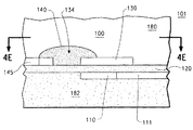
図3は、プリント配線板1000の一部分の第1の実施形態の断面図である。プリント配線板断面1000は、抵抗機能およびコンデンサ機能が単一の容量性/抵抗性デバイス100内に統合されているRC伝送ライン終端を含む。デバイス100は、プリント配線板断面1000内に埋め込まれる。デバイス100は、底部電極110、誘電体120、頂部電極または頂部プレート130、抵抗要素140、導電性トレース145を備える。デバイス100は、中括弧101によって全体的に示される単一のラミネート構造内に抵抗性機能および容量性機能を設ける。
FIG. 3 is a cross-sectional view of a part of the printed
デバイス100は、誘電層180、182を介して延びるめっきスルーホールバイア150と、導電性回路トレース160とによって、ICデバイス170に結合される。ICデバイス170は、はんだパッド172とはんだ継手174によって導電性回路トレース160に接続される。しかし、他の接続技術を使用することもできる。底部電極110は、プリント配線板内の導電性グランドプレーンとしても働くことができ、他の回路に接続する導電性回路トレース111に結合することができる。
図4A〜4Fは、デバイス100を含めて、コンデンサラミネートを作製する方法を示す。
4A-4F illustrate a method of making a capacitor laminate, including the
図4Aは、第1および第2の金属箔112、132が設けられる製造の第1段階の正面断面図である。箔112、132は、たとえば、銅、銅を主成分とする材料、および他の金属から作ることができる。スラリー材料または溶液を第1の箔112上にキャスティングまたは被覆し、乾燥および硬化させ、第1の誘電層124を形成することができる。硬化は、スラリーが熱可塑性のものである場合、たとえば150℃で乾燥することによって行うことができる。スラリーが熱硬化性材料である場合、より高い硬化温度を使用することができる。同様の第2の誘電層126が、第2の箔132上で同様の形で形成される。
FIG. 4A is a front cross-sectional view of a first stage of manufacture in which first and
誘電層124、126を形成するために使用される溶液は、たとえば、溶媒内で溶解されたポリマーを含むことができる。スラリー材料は、高誘電率(ハイK)フィラーまたは機能相を有するポリマー溶媒溶液を含むことができる。スラリーまたは溶液として好適なポリマーは、たとえば、エポキシ樹脂またはポリイミド樹脂を含むことができる。ハイK機能相は、500を超える誘電率を有する材料として定義されることができ、一般式ABO3のペロブスカイトを含むことができる。好適なフィラーには、たとえば、結晶性チタン酸バリウム(BT)、チタン酸バリウム・ストロンチウム(BST)、チタン酸ジルコン酸鉛(PZT)、チタン酸ランタン鉛、チタン酸ジルコン酸ランタン鉛(PLZT)、ニオブ酸マグネシウム鉛(PMN)、チタン酸カルシウム銅が含まれる。フィラーは、粉末形態とすることができる。
The solution used to form the
(図4Aでは誘電層126上で示されている)一方または両方の誘電層124、126の表面に、薄い接着層127を被着させることができる。接着層127は、熱可塑性ポリマーから形成することができ、誘電率が薄まるのを回避するために高誘電相で充填することができる。次いで、2つの構造は、図4Aで矢印によって示されている方向で熱と圧力を受けて、共に積層される。
A thin
図4Bを参照すると、積層により、層124、126、127から単一の誘電体120が形成される。接着層127は、積層プロセス中に誘電層124および126の接合を容易にする。しかし、接着層127は、誘電層124および126が積層前に部分的に硬化されるにすぎず、あるいは熱可塑性のものであり、それにより、積層したとき適切な温度と圧力により樹脂が十分軟化し、その結果、層124および126が接着剤なしで接着する場合、省略することができる。得られる誘電体120は、たとえば、積層後4〜25ミクロン程度の薄い層とすることができる。
Referring to FIG. 4B, a single dielectric 120 is formed from
誘電体120を形成する代替の方法は、フィラー入り(filled)、またはフィラーなしの(unfilled)熱可塑性ポリマーを箔112、132の一方上にキャスティングすること、および他方の箔をフィラー入り熱可塑性ポリマーに直接積層することとすることができる。この方法は、接着層を不要にする。他の代替の製造方法は、誘電層120を単一の膜として別々に形成し、熱と圧力を使用して、第1の箔112および第2の箔132に積層することを含む。
An alternative method of forming the dielectric 120 is to cast a filled or unfilled thermoplastic polymer onto one of the
たとえば(デラウェア州ウィルミントンのDuPont Electronic Technologiesより入手可能な)ポリイミド誘電体INTERRA(商標)HK04など、フィラーなしのポリマーを使用し、誘電体120を形成することができる。 For example, a polymer without a filler, such as the polyimide dielectric INTERRA ™ HK04 (available from DuPont Electronic Technologies, Wilmington, Del.), Can be used to form the dielectric 120.
積層後、標準的な配線板プリント処理条件を使用して、(図4Bには示されていない)フォトレジストが箔112に被着され、箔112がイメージングおよびエッチングされ、残りのフォトレジストが剥離される。図4Cは、図4Dの線4C−4C上で取られた、エッチング後の得られるものの底部断面図である。図4Cを参照すると、エッチングにより、デバイス100の底部電極110ができる。底部電極110を接地または他の回路に接続するために、導電性回路トレース111もまた箔112から形成することができる。
After lamination, photoresist (not shown in FIG. 4B) is applied to foil 112,
図4Dは、図4Cの線4D−4D上で取られた正面断面図である。図4Dを参照すると、得られる物品の底部電極110側は、誘電ラミネート材料182に積層される。積層は、標準的な配線板プリントプロセスにおいて、たとえば、FR4プリプレグまたは他のプリプレグを使用して行うことができる。
4D is a front cross-sectional view taken on line 4D-4D of FIG. 4C. Referring to FIG. 4D, the
(図4Dには示されていない)フォトレジストが箔132に被着され、箔132がイメージングおよびエッチングされ、残りのフォトレジストが剥離される。図4Eは、図4Fの線4E−4E上で取られた、エッチング後の得られる物品の頂部断面図である。図4Fは、図4Eの線4F−4F上で取られた、得られる物品の正面断面図である。図4Eを参照すると、エッチングにより、デバイス100の頂部電極130、間隙134、導電性回路トレース145ができる。
Photoresist (not shown in FIG. 4D) is applied to the
図4Fを参照すると、誘電体120を覆って間隙134内に抵抗材料を堆積することによって、抵抗要素140が形成される。抵抗要素140は、たとえば、ポリマー厚膜抵抗ペーストを堆積し、その抵抗ペーストを硬化させることによって形成することができる。頂部電極130および導電性回路トレース145は、抵抗要素140用の終端として働く。ポリマー厚膜抵抗ペーストは、たとえば、スクリーン印刷用溶剤内に分散された炭素粉末など、諸材料から作ることができる。スクリーン印刷用溶剤は、たとえば、適切な溶媒内で溶解されたエポキシ樹脂を含むことができる。界面活性剤など他の添加剤を追加し、得られる抵抗要素140の誘電特性を修正することができる。
Referring to FIG. 4F, the
抵抗要素140を硬化させた後で、誘電層180が誘電層182の構成部品側に積層され、ラミネート構造101を形成する。次いで、上記のプロセスから得られるラミネート構造101は、たとえば、従来の積層を使用して、また形成プロセスを介して、図3に示されているプリント配線板内に組み込むことができる。
After curing
(実施例1)
デバイス100のこの実施例は、図3を 参照して論じられる。この実施例では、電極110、130は銅箔から形成され、誘電体120は、誘電率(Dk)3.5を有する厚さ25ミクロンのフィラーなしのポリイミド誘電体であり、それによって1平方インチ(6.4516cm2)当たり800ピコファラドの静電容量密度を生み出す(デラウェア州ウィルミントンのDuPont Electronic Technologiesより入手可能なINTERRA(商標)HK04)。
Example 1
This embodiment of
30ピコファラドの伝送ライン終端に必要とされるコンデンサのサイズは、(平面図で見たとき)24.2mm2であり、これは5mm×5mmよりわずかに小さいものに対応する。堆積される抵抗材料は、(DuPont Electronicsより入手可能な)スクリーン印刷可能な100Ω/sqポリマー厚膜抵抗ペーストである。 The required capacitor size for a 30 picofarad transmission line termination (when viewed in plan) is 24.2 mm 2 , which corresponds to a slightly smaller than 5 mm × 5 mm. The resistive material deposited is a screen printable 100 Ω / sq polymer thick film resistive paste (available from DuPont Electronics).
抵抗公称60オーム用の、この実施例における抵抗のサイズは、好ましくは長さ対幅比を約0.6〜1.0の範囲内で維持して変えることができる。上記のコンデンササイズは、ICに必要とされる終端抵抗が比較的少ない場合、許容される。大量の終端が必要とされる場合には、より高い静電容量密度を有するラミネートのほうが、コンデンサをより小さくすることができるため、より望ましい。 The size of the resistor in this example, for a nominal resistance of 60 ohms, can preferably be varied while maintaining a length to width ratio in the range of about 0.6 to 1.0. The above capacitor size is acceptable if the termination resistance required for the IC is relatively small. If a large amount of termination is required, a laminate with a higher capacitance density is more desirable because it can make the capacitor smaller.
(実施例2)
デバイス100の実施例2は、図3を参照して論じられる。この実施例2では、チタン酸バリウムで充填された熱可塑性ポリイミドを銅箔上でキャスティングし、第2の銅箔を、チタン酸バリウムで充填された熱可塑性ポリイミド被覆の表面上に積層することによって、ラミネートが形成される。チタン酸バリウムは、容易に入手可能であり、無鉛であるため、フィラーとして有利である。
(Example 2)
Example 2 of
積層は、別個の接着材料を使用することなしに物品同士が接着するように、適切な温度と圧力で行われる。電極110、130は銅箔から形成され、誘電体120は、誘電率(Dk)11を有する厚さ14ミクロンのフィラー入りポリイミド誘電体であり、それによって1平方インチ(6.4516cm2)当たり4.5ナノファラドの静電容量密度を生み出す(DuPont Electronic Technologiesより入手可能なINTERRA(商標)HK11)。
Lamination is performed at an appropriate temperature and pressure so that the articles adhere without using a separate adhesive material. The
上述の伝送ライン終端に必要とされるコンデンサのサイズは、4.3mm2、または約2mm×2mmである。堆積される抵抗は、(DuPont Electronicsより入手可能な)スクリーン印刷型100Ω/sqポリマー厚膜抵抗ペーストである。 The size of the capacitor required for the above transmission line termination is 4.3 mm 2 , or about 2 mm × 2 mm. The resistor deposited is a screen printed 100 Ω / sq polymer thick film resistor paste (available from DuPont Electronics).
抵抗公称60オーム用の、この実施例2における抵抗の好ましいサイズは、長さ対幅縦横比0.6対1.0を有して、長さ1.2mm、幅2mmである。 The preferred size of resistor in this Example 2 for a nominal resistance of 60 ohms is 1.2 mm long and 2 mm wide with a length to width aspect ratio of 0.6 to 1.0.
(実施例3)
デバイス100のこの実施例3は、図3を参照して論じられる。この実施例3では、ラミネートは、(DuPont Electronic Technologiesより入手可能な)チタン酸バリウムで充填された熱可塑性ポリイミドを2枚の銅箔上でキャスティングし、適切な温度と圧力でそれらを共に積層し共に接着することによって作られる。別個の接着材料は使用されない。電極110、130は、銅箔から形成される。得られる誘電体120は、1平方インチ(6.4516cm2)当たり6.2ナノファラドの静電容量密度を有する厚さ8ミクロンの、チタン酸バリウムで充填されたポリイミド誘電体である。
(Example 3)
This embodiment 3 of the
上述の伝送ライン終端に必要とされるコンデンサのサイズは、3.1mm2、または約1.77mm×1.77mmである。堆積される抵抗は、(DuPont Electronicsより入手可能な)スクリーン印刷型100Ω/sqポリマー厚膜抵抗ペーストから形成することができる。 The size of the capacitor required for the above transmission line termination is 3.1 mm 2 , or about 1.77 mm × 1.77 mm. The deposited resistance can be formed from a screen-printed 100 Ω / sq polymer thick film resistor paste (available from DuPont Electronics).
この実施例における抵抗公称60オーム用の抵抗の好ましいサイズは、長さ対幅縦横比0.6対1.0を有して、長さ1.06mm、幅1.77mmとなることになる。 The preferred size of the nominal 60 ohm resistor in this example would have a length to width aspect ratio of 0.6 to 1.0, resulting in a length of 1.06 mm and a width of 1.77 mm.
上記の諸実施形態によれば、抵抗と組み合わせた薄いコンデンサラミネート構造を使用し、埋込みコンデンサ機能のサイズを削減する、またRC伝送ライン終端をより効果的に埋めることができる。コンデンサ機能および抵抗機能を埋め込むことにより、貴重な基板表面積が解放され、SMTデバイスに関連するはんだ継手がなくなり、それによって信頼性が改善される。さらに、ラミネート内で抵抗と静電容量を組み合わせるラミネートは、従来のエッチングプロセスを使用して処理することができ、これにより生産コストが削減される。 According to the above embodiments, a thin capacitor laminate structure combined with resistors can be used to reduce the size of the embedded capacitor function and more effectively fill the RC transmission line termination. By embedding the capacitor function and the resistor function, valuable substrate surface area is released and the solder joints associated with the SMT device are eliminated, thereby improving reliability. Further, laminates that combine resistance and capacitance within the laminate can be processed using conventional etching processes, thereby reducing production costs.
また、上記の諸実施形態は、回路設計者およびPWB作製者に他のオプションを提供する。たとえば、1枚のラミネートを使用し、ディスクリート抵抗およびディスクリートコンデンサを埋め込むことができ、これにより、抵抗とコンデンサとを接続することに関連するインダクタンスが低減される。 The above embodiments also provide other options for circuit designers and PWB creators. For example, a single laminate can be used to embed discrete resistors and discrete capacitors, which reduces the inductance associated with connecting the resistors and capacitors.
上記の諸実施形態によれば、抵抗と組み合わせた薄いコンデンサラミネート構造を使用して、埋込みコンデンサ機能のサイズを削減し、かつRC伝送ライン終端をより効果的に埋めることができる。コンデンサ機能および抵抗機能を埋め込むことにより、貴重な基板表面積が解放され、SMTデバイスに関連するはんだ継手がなくなり、それによって信頼性が改善される。さらに、ラミネート内で抵抗と静電容量を組み合わせるラミネートは、従来のエッチングプロセスを使用して処理することができ、これにより生産コストが削減される。 According to the above embodiments, a thin capacitor laminate structure combined with a resistor can be used to reduce the size of the embedded capacitor function and more effectively fill the RC transmission line termination. By embedding the capacitor function and the resistor function, valuable substrate surface area is released and the solder joints associated with the SMT device are eliminated, thereby improving reliability. Further, laminates that combine resistance and capacitance within the laminate can be processed using conventional etching processes, thereby reducing production costs.
また、上記の諸実施形態は、回路設計者およびPWB作製者に他のオプションを提供する。たとえば、1枚のラミネートを使用し、多数のディスクリート抵抗および多数のディスクリートコンデンサを埋め込むことができ、これにより、抵抗とコンデンサとを接続することに関連するインダクタンスが低減される。 The above embodiments also provide other options for circuit designers and PWB creators. For example, a single laminate can be used to embed multiple discrete resistors and multiple discrete capacitors, thereby reducing the inductance associated with connecting the resistors and capacitors.
平面図におけるコンデンサ実施形態の形状は、概して矩形である。しかし、コンデンサ電極、誘電体、ならびに他の構成部品および層は、たとえば円形、細長いもの(oblong)、楕円(oval)、または多角形など、他の規則的または不規則な表面領域形状を有することができる。 The shape of the capacitor embodiment in plan view is generally rectangular. However, capacitor electrodes, dielectrics, and other components and layers have other regular or irregular surface area shapes, such as circular, oblong, elliptical, or polygonal, for example. Can do.
単一の容量性/抵抗性デバイス100が上述のラミネート構造101内で形成される。しかし、パネル構造およびプリント配線板は、種類および構成の異なる多数の個々の容量性/抵抗性デバイスを含むことができる。
A single capacitive /
上記の実施形態では、抵抗、静電容量、インダクタンスが組み合わさって、一般に大文字Zによって識別される固有回路インピーダンスを生み出す。抵抗と静電容量とは、ある固有インピーダンスを達成するように構造化することができる。抵抗、静電容量、または両方を変更することにより、インダクタンスが変更されることになる。3つの変更すべてを制御し、最終的なインピーダンスを規定することができる。換言すれば、ラミネートのインピーダンスは「調整可能」である。 In the above embodiment, resistance, capacitance, and inductance combine to produce a unique circuit impedance, generally identified by capital letter Z. Resistance and capacitance can be structured to achieve some inherent impedance. Changing the resistance, capacitance, or both will change the inductance. All three changes can be controlled to define the final impedance. In other words, the impedance of the laminate is “adjustable”.
本発明の前述の説明は、本発明について例示し、述べている。さらに、本開示は、本発明の選択された好ましい実施形態について述べているに過ぎず、本発明は、様々な他の組合せ、修正、環境で使用することが可能であり、上記の教示に対応する、本明細書で述べられている発明性のある概念の範囲内で、かつ/または関連技術の技量または知識内で、変更または修正が可能であることを理解されたい。 The foregoing description of the invention illustrates and describes the present invention. Further, the present disclosure only describes selected preferred embodiments of the present invention, and the present invention can be used in various other combinations, modifications, and environments and corresponds to the above teachings. It should be understood that changes and modifications can be made within the inventive concepts described herein and / or within the skill or knowledge of the relevant art.
さらに、上述の諸実施形態は、本発明を実施することについて知られている最良の形態について述べること、また、そのような、または他の実施形態で、また特定の応用例または本発明の使用によって必要とされる様々な修正と共に、当業者が本発明を利用することを可能にすることが意図されている。したがって、本説明は、本発明を本明細書で開示されている形態に限定しないものとする。また、添付の特許請求の範囲は、詳細な説明において明示的に定義されていない代替の諸実施形態を含むように解釈するべきであるものとする。 Furthermore, the above-described embodiments describe the best mode known for practicing the invention, and in such or other embodiments, and specific applications or uses of the invention. It is intended to enable those skilled in the art to utilize the present invention, along with various modifications required by. Accordingly, the description is not intended to limit the invention to the form disclosed herein. Also, it is intended that the appended claims be construed to include alternative embodiments that are not explicitly defined in the detailed description.
25 プリント回路板
40 SMT抵抗
42、52、172 はんだパット
48、58、174 はんだ継手
50 SMTコンデンサ
59、60、70 回路トレース
100 容量性/抵抗性デバイス
110 底部電極
111、160 導電性回路トレース
112、132 金属箔
120 誘電体
130 頂部電極または頂部プレート
140 抵抗要素
145 導電性トレース
150 めっきスルーホールバイア
180、182 誘電層
25 Printed
Claims (15)
前記第1の電極を覆って配置された誘電体と、
前記誘電体上で、前記誘電体に隣接して形成された抵抗要素と、
導電性トレースと、
前記誘電体を覆って配置された、前記抵抗要素と電気接触する第2の電極とを備えた容量性/抵抗性デバイスであって、前記誘電体が、前記第1の電極と前記第2の電極の間に配置されることを特徴とするデバイス。 A first electrode;
A dielectric disposed over the first electrode;
A resistive element formed on and adjacent to the dielectric;
Conductive traces;
A capacitive / resistive device comprising a second electrode in electrical contact with the resistive element disposed over the dielectric, wherein the dielectric comprises the first electrode and the second electrode A device characterized in that it is arranged between electrodes.
プリント配線板の上面に配置された少なくとも1つのICデバイスであって、前記容量性/抵抗性デバイスに電気的に結合されるICデバイスと
を備えたことを特徴とするプリント配線板。 At least one laminate structure according to claim 6;
A printed wiring board comprising: at least one IC device disposed on an upper surface of the printed wiring board, wherein the IC device is electrically coupled to the capacitive / resistive device.
前記第1と第2の金属箔との間で誘電体を形成するステップと、
前記第1の金属箔から第1の電極を形成するステップと、
前記第2の金属箔から第2の電極および導電性トレースを形成するステップと、
前記誘電体に隣接する、かつ前記第2の電極および前記導電性トレースと電気接触する抵抗要素を形成するステップと
を備えたことを特徴とする容量性/抵抗性デバイスを作製する方法。 Providing a first metal foil and a second metal foil;
Forming a dielectric between the first and second metal foils;
Forming a first electrode from the first metal foil;
Forming a second electrode and a conductive trace from the second metal foil;
Forming a resistive element adjacent to the dielectric and in electrical contact with the second electrode and the conductive trace. A method of making a capacitive / resistive device.
前記第1の金属箔および前記第2の金属箔をエッチングし、前記第1および第2の電極を形成するステップと
をさらに備えたことを特徴とする請求項8に記載の方法。 Providing a first metal foil and a second metal foil;
9. The method of claim 8, further comprising: etching the first metal foil and the second metal foil to form the first and second electrodes.
プリント配線板の上面に配置された、前記容量性/抵抗性デバイスに電気的に結合される少なくとも1つのICデバイスを設けるステップと
を備えたことを特徴とするプリント配線板を作製する方法。 Providing at least one laminate structure according to claim 13;
Providing at least one IC device electrically coupled to the capacitive / resistive device disposed on the top surface of the printed wiring board.
前記第1の金属箔を覆ってポリイミド誘電体を形成するステップと、
前記第1の金属箔から第1の電極を形成するステップと、
第1の誘電層を前記第1の電極の側部に積層するステップと、
前記第2の金属箔から第2の電極および導電性トレースを形成するステップであって、前記第2の電極および前記導電性トレースが、前記誘電体を覆って配置されるステップと、
前記ポリイミド誘電体を覆って、前記第2の電極と電気接触する抵抗要素をプリントするステップであって、前記誘電体が、前記第1の電極と前記第2の電極との間に配置されるステップと、
第2の誘電層を前記第2の電極および前記抵抗要素に積層するステップと
を備えたことを特徴とするラミネート構造を作製する方法。
Providing a first metal foil and a second metal foil;
Forming a polyimide dielectric over the first metal foil;
Forming a first electrode from the first metal foil;
Laminating a first dielectric layer on a side of the first electrode;
Forming a second electrode and conductive trace from the second metal foil, wherein the second electrode and the conductive trace are disposed over the dielectric;
Printing a resistive element overlying the polyimide dielectric and in electrical contact with the second electrode, the dielectric being disposed between the first electrode and the second electrode; Steps,
Laminating a second dielectric layer on the second electrode and the resistive element. A method for producing a laminate structure, comprising:
Applications Claiming Priority (1)
| Application Number | Priority Date | Filing Date | Title |
|---|---|---|---|
| US10/967,569 US7436678B2 (en) | 2004-10-18 | 2004-10-18 | Capacitive/resistive devices and printed wiring boards incorporating such devices and methods of making thereof |
Publications (2)
| Publication Number | Publication Date |
|---|---|
| JP2006121088A true JP2006121088A (en) | 2006-05-11 |
| JP2006121088A5 JP2006121088A5 (en) | 2008-12-04 |
Family
ID=35586143
Family Applications (1)
| Application Number | Title | Priority Date | Filing Date |
|---|---|---|---|
| JP2005303552A Pending JP2006121088A (en) | 2004-10-18 | 2005-10-18 | Capacitive resistance device, printed circuit board incorporated with such device, and method of manufacturing the same |
Country Status (7)
| Country | Link |
|---|---|
| US (2) | US7436678B2 (en) |
| EP (2) | EP1648208B1 (en) |
| JP (1) | JP2006121088A (en) |
| KR (1) | KR100812515B1 (en) |
| CN (1) | CN1783378A (en) |
| DE (1) | DE602005015657D1 (en) |
| TW (2) | TW201343017A (en) |
Families Citing this family (44)
| Publication number | Priority date | Publication date | Assignee | Title |
|---|---|---|---|---|
| DE102004020172A1 (en) * | 2004-04-24 | 2005-11-24 | Robert Bosch Gmbh | Monolithic controller for the generator unit of a motor vehicle |
| US7235745B2 (en) * | 2005-01-10 | 2007-06-26 | Endicott Interconnect Technologies, Inc. | Resistor material with metal component for use in circuitized substrates, circuitized substrate utilizing same, method of making said ciruitized substrate, and information handling system utilizing said ciruitized substrate |
| US20060286696A1 (en) * | 2005-06-21 | 2006-12-21 | Peiffer Joel S | Passive electrical article |
| KR100826352B1 (en) * | 2007-01-30 | 2008-05-02 | 삼성전기주식회사 | Embedded capacitor printed circuit board |
| EP2034808A3 (en) * | 2007-08-07 | 2011-04-06 | Delphi Technologies, Inc. | Embedded resistor and capacitor circuit and method of fabricating same |
| CN101661920B (en) * | 2008-08-26 | 2011-06-29 | 欣兴电子股份有限公司 | Chip packaging carrying plate and making method thereof |
| CN103250473B (en) * | 2010-12-06 | 2016-08-31 | 3M创新有限公司 | Composite diode, electronic device and preparation method thereof |
| CN103247860B (en) * | 2012-02-09 | 2017-08-25 | 深圳光启创新技术有限公司 | The preparation method and Meta Materials of a kind of Meta Materials |
| US9560737B2 (en) | 2015-03-04 | 2017-01-31 | International Business Machines Corporation | Electronic package with heat transfer element(s) |
| US10426037B2 (en) | 2015-07-15 | 2019-09-24 | International Business Machines Corporation | Circuitized structure with 3-dimensional configuration |
| CN105047411A (en) * | 2015-08-12 | 2015-11-11 | 深圳市槟城电子有限公司 | Module with interconnected resistor and capacitor and fabrication method thereof |
| CN105047642B (en) * | 2015-08-12 | 2024-01-19 | 深圳市槟城电子股份有限公司 | Port protection circuit integrated package |
| US10175064B2 (en) | 2015-09-25 | 2019-01-08 | International Business Machines Corporation | Circuit boards and electronic packages with embedded tamper-respondent sensor |
| US9894749B2 (en) | 2015-09-25 | 2018-02-13 | International Business Machines Corporation | Tamper-respondent assemblies with bond protection |
| US9578764B1 (en) | 2015-09-25 | 2017-02-21 | International Business Machines Corporation | Enclosure with inner tamper-respondent sensor(s) and physical security element(s) |
| US10172239B2 (en) | 2015-09-25 | 2019-01-01 | International Business Machines Corporation | Tamper-respondent sensors with formed flexible layer(s) |
| US9924591B2 (en) | 2015-09-25 | 2018-03-20 | International Business Machines Corporation | Tamper-respondent assemblies |
| US9911012B2 (en) | 2015-09-25 | 2018-03-06 | International Business Machines Corporation | Overlapping, discrete tamper-respondent sensors |
| US9591776B1 (en) | 2015-09-25 | 2017-03-07 | International Business Machines Corporation | Enclosure with inner tamper-respondent sensor(s) |
| US10098235B2 (en) | 2015-09-25 | 2018-10-09 | International Business Machines Corporation | Tamper-respondent assemblies with region(s) of increased susceptibility to damage |
| US10143090B2 (en) | 2015-10-19 | 2018-11-27 | International Business Machines Corporation | Circuit layouts of tamper-respondent sensors |
| US9978231B2 (en) | 2015-10-21 | 2018-05-22 | International Business Machines Corporation | Tamper-respondent assembly with protective wrap(s) over tamper-respondent sensor(s) |
| US10083781B2 (en) | 2015-10-30 | 2018-09-25 | Vishay Dale Electronics, Llc | Surface mount resistors and methods of manufacturing same |
| US9913389B2 (en) | 2015-12-01 | 2018-03-06 | International Business Corporation Corporation | Tamper-respondent assembly with vent structure |
| US9555606B1 (en) | 2015-12-09 | 2017-01-31 | International Business Machines Corporation | Applying pressure to adhesive using CTE mismatch between components |
| US10327343B2 (en) | 2015-12-09 | 2019-06-18 | International Business Machines Corporation | Applying pressure to adhesive using CTE mismatch between components |
| US9554477B1 (en) | 2015-12-18 | 2017-01-24 | International Business Machines Corporation | Tamper-respondent assemblies with enclosure-to-board protection |
| US9916744B2 (en) | 2016-02-25 | 2018-03-13 | International Business Machines Corporation | Multi-layer stack with embedded tamper-detect protection |
| US9904811B2 (en) | 2016-04-27 | 2018-02-27 | International Business Machines Corporation | Tamper-proof electronic packages with two-phase dielectric fluid |
| CN107340900B (en) * | 2016-04-29 | 2020-09-18 | 北京小米移动软件有限公司 | Mobile terminal middle frame and mobile terminal |
| US9881880B2 (en) | 2016-05-13 | 2018-01-30 | International Business Machines Corporation | Tamper-proof electronic packages with stressed glass component substrate(s) |
| US9913370B2 (en) | 2016-05-13 | 2018-03-06 | International Business Machines Corporation | Tamper-proof electronic packages formed with stressed glass |
| US9858776B1 (en) | 2016-06-28 | 2018-01-02 | International Business Machines Corporation | Tamper-respondent assembly with nonlinearity monitoring |
| US10321589B2 (en) | 2016-09-19 | 2019-06-11 | International Business Machines Corporation | Tamper-respondent assembly with sensor connection adapter |
| US10299372B2 (en) | 2016-09-26 | 2019-05-21 | International Business Machines Corporation | Vented tamper-respondent assemblies |
| US10271424B2 (en) | 2016-09-26 | 2019-04-23 | International Business Machines Corporation | Tamper-respondent assemblies with in situ vent structure(s) |
| US9999124B2 (en) | 2016-11-02 | 2018-06-12 | International Business Machines Corporation | Tamper-respondent assemblies with trace regions of increased susceptibility to breaking |
| US10640879B2 (en) * | 2016-11-18 | 2020-05-05 | Hutchinson Technology Incorporated | High aspect ratio electroplated structures and anisotropic electroplating processes |
| US10327329B2 (en) | 2017-02-13 | 2019-06-18 | International Business Machines Corporation | Tamper-respondent assembly with flexible tamper-detect sensor(s) overlying in-situ-formed tamper-detect sensor |
| US10438729B2 (en) | 2017-11-10 | 2019-10-08 | Vishay Dale Electronics, Llc | Resistor with upper surface heat dissipation |
| US10306753B1 (en) | 2018-02-22 | 2019-05-28 | International Business Machines Corporation | Enclosure-to-board interface with tamper-detect circuit(s) |
| US11122682B2 (en) | 2018-04-04 | 2021-09-14 | International Business Machines Corporation | Tamper-respondent sensors with liquid crystal polymer layers |
| DE102018127428B3 (en) * | 2018-11-02 | 2020-02-20 | Johnson Electric Germany GmbH & Co. KG | Diagnostic switch, in particular diagnostic micro signal switch and method for its manufacture |
| US20210345481A1 (en) * | 2020-04-29 | 2021-11-04 | Qualcomm Incorporated | Integral super-capacitor for low power applications |
Citations (4)
| Publication number | Priority date | Publication date | Assignee | Title |
|---|---|---|---|---|
| JPS63278399A (en) * | 1987-05-11 | 1988-11-16 | Japan Radio Co Ltd | Composing method for mixed thick film circuit |
| JPH03125416A (en) * | 1989-10-09 | 1991-05-28 | Nippon Oil & Fats Co Ltd | Circuit board |
| JPH11150374A (en) * | 1997-11-18 | 1999-06-02 | Sony Corp | Multilayer wiring board and manufacture thereof |
| JP2004072056A (en) * | 2002-06-14 | 2004-03-04 | Clover Denshi Kogyo Kk | Method of manufacturing laminated printed wiring board |
Family Cites Families (32)
| Publication number | Priority date | Publication date | Assignee | Title |
|---|---|---|---|---|
| US3934119A (en) | 1974-09-17 | 1976-01-20 | Texas Instruments Incorporated | Electrical resistance heaters |
| US4093036A (en) * | 1976-09-07 | 1978-06-06 | Knutson Glenn C | Irrigation tower drive |
| US4377652A (en) | 1978-02-17 | 1983-03-22 | Asahi Kasei Kogyo Kabushiki Kaisha | Polyamide-imide compositions and articles for electrical use prepared therefrom |
| US4410867A (en) * | 1978-12-28 | 1983-10-18 | Western Electric Company, Inc. | Alpha tantalum thin film circuit device |
| US4399417A (en) * | 1980-06-06 | 1983-08-16 | Bell Telephone Laboratories, Incorporated | Integrated CRC filter circuit |
| US4407883A (en) | 1982-03-03 | 1983-10-04 | Uop Inc. | Laminates for printed circuit boards |
| JPS58190091A (en) | 1982-04-30 | 1983-11-05 | 宇部興産株式会社 | Method of producing flexible circuit board |
| JPS59144162A (en) | 1983-02-08 | 1984-08-18 | Nec Corp | Manufacture of thin film circuit |
| JPS60113993A (en) * | 1983-11-25 | 1985-06-20 | 三菱電機株式会社 | Method of producing multilayer circuit board |
| US5093036A (en) | 1988-09-20 | 1992-03-03 | Raychem Corporation | Conductive polymer composition |
| JP3019541B2 (en) | 1990-11-22 | 2000-03-13 | 株式会社村田製作所 | Wiring board with built-in capacitor and method of manufacturing the same |
| JPH0565456A (en) | 1991-09-09 | 1993-03-19 | Sumitomo Bakelite Co Ltd | Resin paste for airtight sealing |
| JPH05152111A (en) * | 1991-11-28 | 1993-06-18 | Rohm Co Ltd | Chip-shaped composite component |
| EP0588136B1 (en) | 1992-09-15 | 1996-11-13 | E.I. Du Pont De Nemours And Company | Polymer thick film resistor compositions |
| US6140402A (en) | 1993-07-30 | 2000-10-31 | Diemat, Inc. | Polymeric adhesive paste |
| US6111005A (en) | 1993-07-30 | 2000-08-29 | Diemat, Inc. | Polymeric adhesive paste |
| JP3117175B2 (en) | 1994-02-09 | 2000-12-11 | アルプス電気株式会社 | Resistor |
| TW301843B (en) | 1994-11-15 | 1997-04-01 | Ibm | Electrically conductive paste and composite and their use as an electrically conductive connector |
| TW367621B (en) | 1995-02-27 | 1999-08-21 | Nxp Bv | Electronic component comprising a thin-film structure with passive elements |
| JPH08306503A (en) * | 1995-05-11 | 1996-11-22 | Rohm Co Ltd | Chip-like electronic part |
| JPH0992983A (en) * | 1995-07-17 | 1997-04-04 | Sumitomo Kinzoku Electro Device:Kk | Manufacture of ceramic multilayer board |
| US5699224A (en) * | 1995-10-25 | 1997-12-16 | Rohm Co., Ltd. | Thick-film capacitor and chip-type composite electronic component utilizing the same |
| US5993698A (en) | 1997-11-06 | 1999-11-30 | Acheson Industries, Inc. | Electrical device containing positive temperature coefficient resistor composition and method of manufacturing the device |
| JP4297617B2 (en) * | 1999-03-17 | 2009-07-15 | モトローラ・インコーポレイテッド | How to make a resistor |
| US6030553A (en) | 1999-04-01 | 2000-02-29 | Industrial Technology Research Institute | Polymer thick film resistor pastes |
| US6535398B1 (en) * | 2000-03-07 | 2003-03-18 | Fujitsu Limited | Multichip module substrates with buried discrete capacitors and components and methods for making |
| US6278356B1 (en) * | 2000-05-17 | 2001-08-21 | Compeq Manufacturing Company Limited | Flat, built-in resistors and capacitors for a printed circuit board |
| US6541137B1 (en) | 2000-07-31 | 2003-04-01 | Motorola, Inc. | Multi-layer conductor-dielectric oxide structure |
| JP2002252297A (en) * | 2001-02-23 | 2002-09-06 | Hitachi Ltd | Electronic circuit device using multilayer circuit board |
| US6910264B2 (en) | 2003-01-03 | 2005-06-28 | Phoenix Precision Technology Corp. | Method for making a multilayer circuit board having embedded passive components |
| JP2004214573A (en) | 2003-01-09 | 2004-07-29 | Murata Mfg Co Ltd | Manufacturing method for multilayered ceramic substrate |
| JP4449772B2 (en) * | 2004-04-09 | 2010-04-14 | 株式会社デンソー | Power semiconductor switching element and semiconductor power module using the same |
-
2004
- 2004-10-18 US US10/967,569 patent/US7436678B2/en active Active
-
2005
- 2005-09-26 EP EP05020897A patent/EP1648208B1/en active Active
- 2005-09-26 DE DE602005015657T patent/DE602005015657D1/en active Active
- 2005-09-26 EP EP09007939A patent/EP2104407A1/en not_active Withdrawn
- 2005-10-04 TW TW102121911A patent/TW201343017A/en unknown
- 2005-10-04 TW TW094134607A patent/TWI412306B/en active
- 2005-10-17 KR KR1020050097354A patent/KR100812515B1/en active IP Right Grant
- 2005-10-18 CN CNA2005101161073A patent/CN1783378A/en active Pending
- 2005-10-18 JP JP2005303552A patent/JP2006121088A/en active Pending
-
2007
- 2007-01-26 US US11/698,423 patent/US7571536B2/en active Active
Patent Citations (4)
| Publication number | Priority date | Publication date | Assignee | Title |
|---|---|---|---|---|
| JPS63278399A (en) * | 1987-05-11 | 1988-11-16 | Japan Radio Co Ltd | Composing method for mixed thick film circuit |
| JPH03125416A (en) * | 1989-10-09 | 1991-05-28 | Nippon Oil & Fats Co Ltd | Circuit board |
| JPH11150374A (en) * | 1997-11-18 | 1999-06-02 | Sony Corp | Multilayer wiring board and manufacture thereof |
| JP2004072056A (en) * | 2002-06-14 | 2004-03-04 | Clover Denshi Kogyo Kk | Method of manufacturing laminated printed wiring board |
Also Published As
| Publication number | Publication date |
|---|---|
| TW201343017A (en) | 2013-10-16 |
| KR100812515B1 (en) | 2008-03-11 |
| US20060082981A1 (en) | 2006-04-20 |
| KR20060054033A (en) | 2006-05-22 |
| US7571536B2 (en) | 2009-08-11 |
| CN1783378A (en) | 2006-06-07 |
| DE602005015657D1 (en) | 2009-09-10 |
| EP1648208A1 (en) | 2006-04-19 |
| EP2104407A1 (en) | 2009-09-23 |
| US7436678B2 (en) | 2008-10-14 |
| US20070139901A1 (en) | 2007-06-21 |
| EP1648208B1 (en) | 2009-07-29 |
| TWI412306B (en) | 2013-10-11 |
| TW200628024A (en) | 2006-08-01 |
Similar Documents
| Publication | Publication Date | Title |
|---|---|---|
| US7571536B2 (en) | Method of making capacitive/resistive devices | |
| JP4500759B2 (en) | Capacitive / resistive devices, high dielectric constant organic dielectric laminates, printed wiring boards incorporating such devices, and methods of making the same | |
| KR100754714B1 (en) | Power core devices and methods of making thereof | |
| JP4970789B2 (en) | Capacitive devices, organic dielectric laminates, printed wiring boards incorporating such devices, and methods for their production | |
| KR101401863B1 (en) | Printed Circuit Board With Embeded Capacitor And Fabricating Method Thereof | |
| US7813141B2 (en) | Capacitive/resistive devices, organic dielectric laminates and printed wiring boards incorporating such devices, and methods of making thereof | |
| JP2006179923A (en) | Electric power core device and method for fabricating the same | |
| US20060098386A1 (en) | Embedded capacitor and method for manufacturing the same | |
| JP4207517B2 (en) | Embedded substrate | |
| JPH1056251A (en) | Printed board with built-in electronic component and its production | |
| JP4269657B2 (en) | Dielectric multilayer sheet, capacitor sheet with built-in substrate, and substrate with built-in element | |
| JP4684483B2 (en) | Multilayer circuit board manufacturing method | |
| JP2002217553A (en) | Multilayer printed wiring substrate and manufacturing method of the multilayer printed wiring board |
Legal Events
| Date | Code | Title | Description |
|---|---|---|---|
| A521 | Written amendment |
Free format text: JAPANESE INTERMEDIATE CODE: A523 Effective date: 20081020 |
|
| A621 | Written request for application examination |
Free format text: JAPANESE INTERMEDIATE CODE: A621 Effective date: 20081020 |
|
| A131 | Notification of reasons for refusal |
Free format text: JAPANESE INTERMEDIATE CODE: A131 Effective date: 20100709 |
|
| A601 | Written request for extension of time |
Free format text: JAPANESE INTERMEDIATE CODE: A601 Effective date: 20101012 |
|
| A602 | Written permission of extension of time |
Free format text: JAPANESE INTERMEDIATE CODE: A602 Effective date: 20101015 |
|
| A601 | Written request for extension of time |
Free format text: JAPANESE INTERMEDIATE CODE: A601 Effective date: 20101109 |
|
| A602 | Written permission of extension of time |
Free format text: JAPANESE INTERMEDIATE CODE: A602 Effective date: 20101117 |
|
| A521 | Written amendment |
Free format text: JAPANESE INTERMEDIATE CODE: A523 Effective date: 20101209 |
|
| A02 | Decision of refusal |
Free format text: JAPANESE INTERMEDIATE CODE: A02 Effective date: 20110610 |