EP2104022B1 - One layer capacitive sensing apparatus having varying width sensing elements - Google Patents
One layer capacitive sensing apparatus having varying width sensing elements Download PDFInfo
- Publication number
- EP2104022B1 EP2104022B1 EP09007787A EP09007787A EP2104022B1 EP 2104022 B1 EP2104022 B1 EP 2104022B1 EP 09007787 A EP09007787 A EP 09007787A EP 09007787 A EP09007787 A EP 09007787A EP 2104022 B1 EP2104022 B1 EP 2104022B1
- Authority
- EP
- European Patent Office
- Prior art keywords
- sensing element
- sensing
- axis
- sensor pattern
- capacitive sensor
- Prior art date
- Legal status (The legal status is an assumption and is not a legal conclusion. Google has not performed a legal analysis and makes no representation as to the accuracy of the status listed.)
- Active
Links
- 230000001186 cumulative effect Effects 0.000 claims abstract description 16
- 239000000758 substrate Substances 0.000 claims description 16
- 239000004020 conductor Substances 0.000 claims description 12
- RYGMFSIKBFXOCR-UHFFFAOYSA-N Copper Chemical compound [Cu] RYGMFSIKBFXOCR-UHFFFAOYSA-N 0.000 claims description 3
- 238000010276 construction Methods 0.000 claims description 3
- 229910052802 copper Inorganic materials 0.000 claims description 3
- 239000010949 copper Substances 0.000 claims description 3
- 230000008878 coupling Effects 0.000 description 27
- 238000010168 coupling process Methods 0.000 description 27
- 238000005859 coupling reaction Methods 0.000 description 27
- 239000000523 sample Substances 0.000 description 15
- 238000005516 engineering process Methods 0.000 description 5
- 239000010410 layer Substances 0.000 description 5
- 238000004519 manufacturing process Methods 0.000 description 4
- NCGICGYLBXGBGN-UHFFFAOYSA-N 3-morpholin-4-yl-1-oxa-3-azonia-2-azanidacyclopent-3-en-5-imine;hydrochloride Chemical compound Cl.[N-]1OC(=N)C=[N+]1N1CCOCC1 NCGICGYLBXGBGN-UHFFFAOYSA-N 0.000 description 3
- 230000008901 benefit Effects 0.000 description 3
- 238000001514 detection method Methods 0.000 description 3
- 238000000034 method Methods 0.000 description 3
- 238000012986 modification Methods 0.000 description 3
- 230000004048 modification Effects 0.000 description 3
- 238000006243 chemical reaction Methods 0.000 description 2
- 239000011152 fibreglass Substances 0.000 description 2
- 239000011521 glass Substances 0.000 description 2
- 230000003287 optical effect Effects 0.000 description 2
- 239000004033 plastic Substances 0.000 description 2
- 241001481828 Glyptocephalus cynoglossus Species 0.000 description 1
- 230000000295 complement effect Effects 0.000 description 1
- 230000000694 effects Effects 0.000 description 1
- AMGQUBHHOARCQH-UHFFFAOYSA-N indium;oxotin Chemical compound [In].[Sn]=O AMGQUBHHOARCQH-UHFFFAOYSA-N 0.000 description 1
- 239000000463 material Substances 0.000 description 1
- 239000002365 multiple layer Substances 0.000 description 1
- 239000002356 single layer Substances 0.000 description 1
Images


Classifications
-
- G—PHYSICS
- G06—COMPUTING; CALCULATING OR COUNTING
- G06F—ELECTRIC DIGITAL DATA PROCESSING
- G06F3/00—Input arrangements for transferring data to be processed into a form capable of being handled by the computer; Output arrangements for transferring data from processing unit to output unit, e.g. interface arrangements
- G06F3/01—Input arrangements or combined input and output arrangements for interaction between user and computer
- G06F3/03—Arrangements for converting the position or the displacement of a member into a coded form
- G06F3/041—Digitisers, e.g. for touch screens or touch pads, characterised by the transducing means
- G06F3/044—Digitisers, e.g. for touch screens or touch pads, characterised by the transducing means by capacitive means
- G06F3/0443—Digitisers, e.g. for touch screens or touch pads, characterised by the transducing means by capacitive means using a single layer of sensing electrodes
-
- G—PHYSICS
- G01—MEASURING; TESTING
- G01R—MEASURING ELECTRIC VARIABLES; MEASURING MAGNETIC VARIABLES
- G01R27/00—Arrangements for measuring resistance, reactance, impedance, or electric characteristics derived therefrom
- G01R27/02—Measuring real or complex resistance, reactance, impedance, or other two-pole characteristics derived therefrom, e.g. time constant
- G01R27/26—Measuring inductance or capacitance; Measuring quality factor, e.g. by using the resonance method; Measuring loss factor; Measuring dielectric constants ; Measuring impedance or related variables
-
- G—PHYSICS
- G06—COMPUTING; CALCULATING OR COUNTING
- G06F—ELECTRIC DIGITAL DATA PROCESSING
- G06F3/00—Input arrangements for transferring data to be processed into a form capable of being handled by the computer; Output arrangements for transferring data from processing unit to output unit, e.g. interface arrangements
- G06F3/01—Input arrangements or combined input and output arrangements for interaction between user and computer
- G06F3/03—Arrangements for converting the position or the displacement of a member into a coded form
- G06F3/041—Digitisers, e.g. for touch screens or touch pads, characterised by the transducing means
- G06F3/044—Digitisers, e.g. for touch screens or touch pads, characterised by the transducing means by capacitive means
- G06F3/0448—Details of the electrode shape, e.g. for enhancing the detection of touches, for generating specific electric field shapes, for enhancing display quality
Definitions
- Conventional computing devices provide several ways for enabling a user to input a choice or a selection. For example, a user can use one or more keys of an alphanumeric keyboard communicatively connected to the computing device in order to indicate a choice or selection. Additionally, a user can use a cursor control device communicatively connected to the computing device to indicate a choice. Also, a user can use a microphone communicatively connected to the computing device to audibly indicate a particular selection. Moreover, touch sensing technology can be used to provide an input selection to a computing device or other electronic device.
- capacitive sensing touch screens there exist capacitive sensing touch screens.
- capacitive sensing touch screens there are different sensing technologies.
- one sensing technology involves the use of sensing electrodes formed in triangular shapes wherein the direction of each triangle point alternates.
- one of the disadvantages is that as a finger (or object) moves towards the wide end of a first triangular shaped electrode and the narrow point of a second triangular shaped electrode, the narrow point electrode does not provide a quality signal because of its inherent signal to noise ratio. As such, this can be referred to as sensing geometry that induces signal to noise ratio concerns.
- Another sensing technology uses a grid of conductive elements that cross over one another. While this design offers ease of signal interpretation, it also has the disadvantage of higher manufacturing cost. A further disadvantage affects multiple-layer sensors, as each layer degrades optical clarity of a capacitive sensing touch screen.
- the present invention may address one or more of the above mentioned issues.
- the two-dimensional capacitive sensor can include a first sensing element having varying width, a second sensing element having varying width, and a third sensing element having varying width. Additionally, the first sensing element, second sensing element, and third sensing element are substantially parallel to a first axis. Furthermore, each of the first sensing element, second sensing element, and third sensing element can be located such that they are not required to overlap each other to determine a first location along the first axis of a two-dimensional space. Moreover, the first sensing element, second sensing element, and third sensing element can have a cumulative width that is substantially constant.
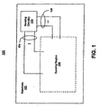
- FIG. 1 is a plan view of an exemplary two-dimensional capacitive sensor apparatus 100 that can be implemented to include one or more embodiments of the present invention.
- the capacitive sensor apparatus 100 can be utilized to communicate user input (e.g., using a user's finger or a probe) to a computing device or other electronic device.
- capacitive sensor apparatus 100 can be implemented as a capacitive touch screen device that can be placed over an underlying image or an information display device (not shown). In this manner, a user would view the underlying image or information display by looking through the substantially transparent sensing region 108 of capacitive sensor apparatus 100 as shown.
- one or more embodiments in accordance with the present invention can be incorporated with a capacitive touch screen device similar to capacitive sensor apparatus 100.
- the capacitive sensor apparatus 100 when implemented as a touch screen can include a substantially transparent substrate 102 having a first set of conductive coupling traces 104 and a second set of conductive coupling traces 106 patterned (or formed) thereon.
- Conductive coupling traces 104 and/or 106 can be utilized for coupling any sensing elements (not shown) or conductive traces that would form a sensing region 108 with sensing circuitry 110 thereby enabling the operation of capacitive sensor apparatus 100.
- Conductive coupling traces 104 and 106 may each include one or more conductive coupling elements or traces. It is noted that embodiments of sensing element patterns in accordance with the invention are described herein which can be implemented to form sensing region 108.
- the capacitive sensor apparatus 100 can also be implemented as a capacitive touchpad device.
- substrate 102 of capacitive sensor apparatus 100 can be implemented with, but is not limited to, one or more opaque materials that are utilized as a substrate for a capacitive touchpad device.
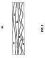
- FIG. 2 is a plan view of an exemplary capacitive sensor pattern 200 in accordance with embodiments of the invention.
- sensor pattern 200 includes sensing elements 202, 204, and 206 having three phases which can be utilized as part of a two-dimensional capacitive sensor apparatus (e.g., 100), such as but not limited to, a touch screen and/or a touchpad.
- sensor pattern 200 provides positioning information from a sensor pattern that has substantially parallel traces (or elements) with no crossovers. The positioning information can be derived from which sensing element detects an object (e.g., a user's finger, a probe, and the like), and the proportional strength of the signals on sensing elements 202, 204, and 206.
- sensing elements 202, 204, and 206 can be oriented using a single layer of conductive material such that they are substantially parallel to a first axis and their capacitive coupling to the sensor surface can vary periodically along the length of each trace (or sensing element).
- the widths of the sensing elements 202, 204, and 206 vary sinusoidally.
- the widths of sensing elements 202, 204, and 206 can each be a sinusoidal function of position.
- the varying width of each sensing element 202, 204, and 206 can include all or a portion of a sinusoidal waveform.
- each sensing element 202, 204, and 206 can include multiple sinusoidal waveforms or any other type of waveform.
- the sum of the widths of traces 202, 204, and 206 can also be implemented as a substantial constant.
- the phases of traces 202, 204, and 206 can each be shifted relative to its neighbors, so that the sum of the traces 202, 204, and 206 produces a complementary set of signals.
- the sensing elements 202, 204, and 206 can differ in phase by any angle (e.g., substantially 24, 30, 36, 40, 45, 60, 72, 90, or 120 degrees, etc.).
- sensing elements 202, 204, and 206 are each implemented to include less than one cycle (or period) of a sinusoidal waveform while each has a different phase. In this manner, each of the sensing elements 202, 204, and 206 produces a unique signal along its length.
- the combination of the output signals produced by the sensing elements 202, 204, and 206 can specifically identify the location of an object (e.g., a user's finger, a probe, a stylus, etc.) along the length of sensor pattern 200. It is noted that the sensing elements 202, 204, and 206 are location such that they are not required to overlap each other in order to determine a first location of an object along the first axis of a two-dimensional space.
- an object e.g., a user's finger, a probe, a stylus, etc.
- the shape and phase of the sensing elements 202, 204, and 206 can be implemented in a wide variety of ways. For example, within the present embodiment, if the waveform shape of sensing element 202 is substantially equal to sin e, then the waveform shape of sensing element 204 may be substantially equal to sin ⁇ + 120 degrees, while the waveform shape of sensing element 206 may be substantially equal to sin ⁇ + 240 degrees. Alternatively, the waveforms of sensing elements 204 and 206 may each be offset from the waveform of sensing element 202 by 2 ⁇ /3 radians. However, it is understood that the phase and shape of the waveform of sensing elements 202, 204, and 206 are not in any way limited to the present embodiment.
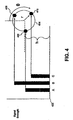
- Figure 4 illustrates an exemplary signal strength chart 402 along with its conversion into polar coordinates in accordance with embodiments of the invention. For example, suppose signal "A” is associated with sensing element 202 ( Figure 2 ), signal “B” is associated with sensing element 204, and signal “C” is associated with sensing element 206.
- the object is located along sensor 200 where sensing trace 204 is the widest, the sensing trace 202 is the second widest, and the sensing trace 206 is the third widest. Therefore, within this example, the object is located near the right-hand end of sensor pattern 200.
- signal "A” corresponds to sensing element 202
- signal “B” corresponds to sensing element 204
- signal “C” corresponds to sensing element 206, as mentioned above.
- sensing elements (or traces) 202, 204, and 206 have been observed to give values A 0 , B 0 , and C 0 , respectively, when no object is present or near sensor pattern 200.
- a A - A 0
- b B - B 0
- c C - C 0 . Therefore, determination of the polar coordinates "h”, "r”, and angle ⁇ that are associated with signals A, B, and C can be performed.
- the value of "h” corresponds to the height of the center of a circle 404 upon which points 406, 408, and 410 can be located.
- the points 406, 408, and 410 are associated with signals A, B, and C, respectively.
- the value of "r” corresponds to the radius of circle 404.
- the value of angle ⁇ can be used to indicate the linear location (or position) of an object in relationship to the length of sensor pattern 200.
- each degree of angle ⁇ may be equal to a specific distance (e.g., a specific number of millimeters or inches) from one of the end points of sensor pattern 200.
- a lookup table may be utilized to ascertain the distance that corresponds to the determined e. It is noted that the angle ⁇ provides the location of the center of the object along sensor pattern 200 while the "h” and the “r” can provide information regarding the size of the object.
- One of the advantages of determining the position along the first axis (e.g., X axis) of sensor pattern 200 in the manner described above is that common-mode noise has no effect on the determination of "r" and ⁇ .
- the sensing elements 202, 204, and 206 of sensor pattern 200 can be fabricated with any conductive material on any insulating substrate (e.g., 102).
- any conductive material on any insulating substrate e.g., 102
- this may include conventional copper/fiberglass printed circuit construction, ITO patterned on glass, screen printed conductor patterned on plastic, and the like.
- the sensor pattern 200 may be used to detect objects on either side of the substrate onto which it is fabricated.
- a ground plane or a driven shield conductor may be utilized to shield that side.
- sensor pattern 200 of Figure 2 there are advantages associated with the sensor pattern 200 of Figure 2 . For example, since the manufacture of sensor pattern 200 involves one layer of conductive material, this reduces manufacturing costs relative to the two-layer X-Y grids often used in touchpads. Additionally, in the case of touch screens, doing all the fabrication using only one layer of conductive material eliminates low yield alignment steps. Furthermore, the optical properties of touch screens can also benefit from the use of only one layer of substantially transparent conductive material, such as indium tin oxide (ITO).
- ITO indium tin oxide
- sensor pattern 200 can be implemented with a greater number of sensing elements than the sensing elements 202, 204, and 206 shown. However, if sensor pattern 200 is implemented with a greater number of sensing elements, the relationships described with reference to Figures 4 and 2 would be modified accordingly in order to determine "h”, "r", and ⁇ .
- sensing elements 202, 204, and 206 of the sensor pattern 200 can individually be coupled with sensing circuitry 110 ( Figure 1 ) utilizing conductive coupling traces 104 and/or 106. When coupled in this manner, the sensor pattern 200 can be utilized to form the sensing region 108.
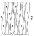
- FIG. 3 is a plan view of an exemplary capacitive sensor pattern 300 in accordance with embodiments of the invention.
- sensor pattern 300 can provide two-dimensional positioning information that has substantially parallel traces (or elements) with no crossovers.
- sensor pattern 300 includes a low-frequency set of sensing elements (e.g., 202, 204, and 206) and a high-frequency set of sensing elements (e.g., 302, 304, and 306). These two sets can work together to provide "coarse” and "fine” positioning information.
- sensing elements 202, 204, and 206 can operate in any manner similar to that described above to provide the "coarse" positioning information corresponding to the linear position of an object (e.g., a user's finger, a probe, and the like) in relation to sensor pattern 300.
- each of the signals associated with sensing elements 202, 204, and 206 can be utilized to determine the angle ⁇ , as described above with reference to Figures 2 and 4 .
- the "coarse" position along the first axis (e.g., X axis) of sensor pattern 300 is determined to the first order.
- the "fine" positioning information, or determination to the second order can be obtained by utilizing sensing elements 302, 304, and 306.
- each of the signals associated with sensing elements 302, 304, and 306. can be utilized to determine a second value ⁇ in a manner similar to that described herein with reference to Figures 2 and 4 .
- sensing elements 302, 304, and 306 include 4 periods (or cycles) of sinusoidal waveforms
- the determined second, value of ⁇ can represent 4 different locations along traces 302, 304, and 306.
- the "coarse" location is known with respect to sensing elements 202, 204, and 206, the second value of ⁇ located closest to the "coarse" location can be used. In this manner, this second order determination provides a finer resolution of the location (or position) of the object in relation to sensor pattern 300.
- sensing elements 202, 204, and 206 of sensor pattern 300 can include a portion of a waveform, along with one or more waveforms. Additionally, sensing elements 302, 304, and 306 of sensor pattern 300 can include any number of waveforms, or a portion of a waveform. It is understood that the sensing elements 302, 304, and 306 can be implemented in any manner that is different than the manner that sensing elements 202, 204, and 206 of sensor pattern 300 are implemented.
- the sensing elements 202, 204, 206, 302, 304, and 306 of sensor pattern 300 can be fabricated with any conductive material on any insulating substrate (e.g., 102).
- any conductive material on any insulating substrate e.g., 102
- this may include conventional copper/fiberglass printed circuit construction, ITO patterned on glass, screen printed conductor patterned on plastic, and the like.
- the sensor pattern 300 may be used to detect objects on either side of the substrate onto which it is fabricated.
- a ground plane or a driven shield conductor may be utilized to shield that side.
- the "low-frequency” (or “coarse") set of sensing elements (e.g., 202, 204, and 206) of sensor pattern 300 can be implemented with a greater number of sensing elements than that shown.
- the "high-frequency” (or “fine”) set of sensing elements (e.g., 302, 304, and 306) of censor pattern 300 can also be implemented with a greater number of sensing elements than that shown.
- the relationships described with reference to Figures 2 and 4 would be modified accordingly in order to determine "h", "r", and ⁇ .
- sensing elements 202, 204, 206, 302, 304, and 306 of the sensor pattern 300 can individually be coupled with sensing circuitry 110 ( Figure 1 ) utilizing conductive coupling traces 104 and/or 106. When coupled in this manner, the sensor pattern 300 can be utilized to form the sensing region 108. It is understood that sensor pattern 300 can be utilized in any manner similar to that described herein, but is not limited to such.
- FIG. 5 is a plan view of an exemplary capacitive sensor pattern 500 in accordance with embodiments of the invention.
- sensor pattern 500 includes three repeated patterns similar to sensing elements 202a, 204a, and 206a having three phases which can be utilized as part of a two-dimensional capacitive sensor apparatus (e.g., 100), such as but not limited to, a touch screen and/or a touchpad.
- sensor pattern 500 can provide two-dimensional positioning information that has substantially parallel traces (or sensing elements) with no crossovers.
- the sensor pattern 500 can be utilized in any manner similar to that described herein with reference to Figures 2 and 4 .
- any set of three adjacent traces can provide the signals for determining first-axis positioning of an object along the length of sensor pattern 500.
- sensor pattern 500 includes nine traces which allows for seven sets of three adjacent traces. It is appreciated that sensor pattern 500 can be utilized in any manner similar to that described herein, but is not limited to such.
- the sensing elements 202a, 204a, 206a, 202b, 204b, 206b, 202c, 204c, and 206c of sensor pattern 500 have been implemented in a different manner than the sensing elements 202, 204, and 206 of Figures 2 and 3 .
- each of the sensing elements 202a, 204a, 206a, 202b, 204b, 206b, 202c, 204c, and 206c does not include straight edges along its length.
- the sum of the widths of a set of sensing elements (e.g., 202a, 204a, and 206a) of sensor pattern 500 can be implemented as a substantial constant.
- each of the nine sensing elements 202a-206c of the sensor pattern 500 can be individually coupled with sensing circuitry 110 ( Figure 1 ) utilizing conductive coupling traces 104 and/or 106.
- the sensor pattern 500 can be utilized to form the sensing region 108.
- sensor pattern 500 can provide positioning information along a first axis (e.g., X axis), as described herein, and along a second axis (e.g., Y axis).
- each of the sensing elements 202a-206c of sensor pattern 500 can be utilized for determining a second location along a second axis (e.g., Y axis) that can be substantially perpendicular (or not parallel) to the first axis (e.g., X axis).
- a second axis e.g., Y axis
- the sensing circuitry e.g., 110 coupled with the sensor pattern 500 can determine that an object is location near sensing element 202a in the Y direction of the two-dimensional space.
- sensing circuitry can determine that an object is located below or near sensing element 206c in the Y direction of the two-dimensional space.
- sensor pattern 500 can be utilized to provide two coordinate positions associated with a two-dimensional space that correspond to the position of an object in relation to the sensor pattern 500.
- all of the similar sensing elements (e.g., 202a, 202b, and 202c) of sensor pattern 500 can be coupled together with sensing circuitry 110 ( Figure 1 ) utilizing conductive coupling traces 104 and/or 106.
- the sensor pattern 500 can provide positioning information to the sensing circuitry 110 corresponding to the first axis (e.g. X axis), but not along the second axis (e.g., Y axis).
- sensor pattern 500 can be implemented with a greater or fewer number of sensing elements than shown within the present embodiment.
- Sensor pattern 500 and its sensing elements 202a, 204a, 206a, 202b, 204b, 206b, 202c, 204c, and 206c can be implemented in any manner similar to that described herein, but is not limited to such.
- each set (e.g., 206a, 202b, and 204b) of the sensing elements (e.g., 202a-206c) of sensor pattern 500 can operate in any manner similar to that described herein in order to provide the positioning information corresponding to the linear position of an object (e.g., a user's finger, a probe, and the like) in relation to sensor pattern 500.
- each set of the signals associated with a set of sensing elements e.g., 204b, 206b, and 202c
- the position (or location) along the first axis (e.g., X axis) of sensor pattern 500 can be determined.
- FIG. 6 is a plan view of an exemplary capacitive sensor pattern 600 in accordance with embodiments of the invention.
- sensor pattern 600 includes five repeated patterns of a set of sensing elements 202, 204, and 206 having three phases which can be utilized as part of a two-dimensional capacitive sensor apparatus (e.g., 100), such as but not limited to, a touch screen and/or a touchpad.
- sensor pattern 600 includes second axis (e.g., Y axis) sensing elements 602 that are substantially parallel to the first axis, and interdigitated with each set of sensing elements 202, 204, and 206, and can be utilized for providing position information along the second axis.
- Sensor pattern 600 can provide two-dimensional positioning information that has substantially parallel traces (or sensing elements) with no crossovers. It is appreciated that sensor pattern 600 can be utilized in any manner similar to that described herein, but is not limited to such.
- Each of the similar first axis sensing elements (e.g., 202) of sensor pattern 600 can be coupled together and coupled with sensing circuitry 110 ( Figure 1 ) utilizing, but not limited to, conductive coupling traces 106. However, each similar first axis sensing element can be coupled together and coupled with sensing circuitry utilizing conductive coupling traces 104 and/or 106. Additionally, each of the second axis sensing elements (e.g., 602) can be coupled independently to sensing circuitry utilizing, but not limited to, conductive coupling traces 104. However, each of the second axis sensing elements 602 can be coupled individually with sensing circuitry utilizing conductive coupling traces 104 and/or 106.
- the second axis sensing elements 602 can operate to provide positioning information corresponding to the second axis position of an object (e.g., a user finger, a probe, a stylus, etc.) relative to sensor pattern 600. Therefore, when coupled in this manner, the sensor pattern 600 can provide positioning information to the sensing circuitry corresponding to the first axis (e.g. X axis) along with the second axis (e.g., Y axis). It is noted that the second axis is not parallel to the first axis and may be substantially perpendicular to it.
- the sensor pattern 600 can be utilized to form the sensing region 108.
- each of the first axis sensing elements (e.g., 202, 204, and 206) of the sensor pattern 600 can be individually coupled with sensing circuitry 110 ( Figure 1 ) utilizing conductive coupling traces 104 and/or 106.
- the sensor pattern 600 can be utilized to form the sensing region 108.
- the first axis sensing elements (e.g., 202, 204, and 206) of sensor pattern 600 can provide positioning information for both the first axis (e.g., X axis) and second axis (e.g., Y axis) since each trace can produce a signal that is individually detected by the sensing circuitry.
- sensor pattern 600 can be implemented without the second axis sensing elements 602.
- Sensor pattern 600 can be implemented with a greater or fewer number of sensing elements than shown within the present embodiment. Sensor pattern 600 and its sensing elements can be implemented in any manner similar to that described herein, but is not limited to such.
- each set of the first axis sensing elements (e.g., 202, 204, and 206) of sensor pattern 600 can operate in any manner similar to that described herein in order to provide the positioning information corresponding to the linear position of an object (e.g., a user's finger, a probe, and the like) in relation to sensor pattern 600.
- each set of the signals associated with a set of sensing elements (e.g., 202, 204, and 206) can be utilized to determine the angle ⁇ , as described above with reference to Figures 2 and 4 . In this manner, the position (or location) along the first axis (e.g., X axis) of sensor pattern 600 is determined.
- FIG. 7 is a plan view of an exemplary capacitive sensor pattern 700 in accordance with embodiments of the invention.
- sensor pattern 700 includes four repeated patterns of "coarse” and “fine” sets of sensing elements 202, 204, 206, 302, 304, and 306 which can be utilized as part of a two-dimensional capacitive sensor apparatus (e.g., 100), such as but not limited to, a touch screen and/or a touchpad.
- a two-dimensional capacitive sensor apparatus e.g., 100
- sensor pattern 700 includes second axis (e.g., Y axis) sensing elements 702 that are substantially parallel to the first axis, interdigitated with each set of sensing elements 202, 204, 206, 302, 304, and 306, and can be utilized for providing position information along the second axis.
- Sensor pattern 700 can provide two-dimensional positioning information that has substantially parallel traces (or sensing elements) with no crossovers. It is noted that sensor pattern 700 can be utilized in any manner similar to that described herein, but is not limited to such.
- Each of the similar first axis sensing elements (e.g., 302) of sensor pattern 700 can be coupled together and coupled with sensing circuitry 110 ( Figure 1 ) utilizing, but not limited to, conductive coupling traces 104. However, each similar first axis sensing element can be coupled together and coupled with sensing circuitry utilizing conductive coupling traces 104 and/or 106. Furthermore, each of the second axis sensing elements (e.g., 702) can be coupled independently to sensing circuitry utilizing, but not limited to, conductive coupling traces 106. However, each of the second axis sensing elements 702 can be coupled individually with sensing circuitry utilizing conductive coupling traces 104 and/or 106.
- the sensor pattern 700 can be utilized to form the sensing region 108. Additionally, when coupled in this manner, the sensor pattern 700 can provide positioning information to the sensing circuitry corresponding to the first axis (e.g. X axis) along with the second axis (e.g., Y axis). It is noted that the second axis is not parallel to the first axis and may be substantially perpendicular to it.
- each of the first axis sensing elements (e.g., 202, 204, 206, 302, 304, and 306) of the sensor pattern 700 can be individually coupled with sensing circuitry 110 ( Figure 1 ) utilizing conductive coupling traces 104 and/or 106. When coupled in this manner, the sensor pattern 700 can be utilized to form the sensing region 108.
- the first axis sensing elements (e.g., 202, 204, 206, 302, 304, and 306) of sensor pattern 700 can provide positioning information for both the first axis (e.g., X axis) and second axis (e.g., Y axis) since each trace can produce a signal that is individually detected by the sensing circuitry.
- sensor pattern 700 can be implemented without the second axis sensing elements 702.
- Sensor pattern 700 can be implemented with a greater or fewer number of sensing elements than shown within the present embodiment. Sensor pattern 700 and its sensing elements can be implemented in any manner similar to that described herein, but is not limited to such.
- each set of the first axis sensing elements (e.g., 202, 204, 206, 302, 304, and 306) of sensor pattern 700 can operate in any manner similar to that described herein to provide the positioning information corresponding to the linear position of an object (e.g., a user's finger, a probe, and the like) in relation to sensor pattern 700.
- each set of the signals associated with a set of sensing elements (e.g., 202, 204, and 206) can be utilized to determine the angle ⁇ , as described above with reference to Figures 2 and 4 . In this manner, the position (or location) along the first axis (e.g., X axis) of sensor pattern 700 is determined.
- FIG 8 is a plan view of an exemplary capacitive sensor pattern 800 in accordance with embodiments of the invention.
- sensor pattern 800 includes guard traces 802 and 804 along with five repeated patterns of sensing elements 202a, 204a, and 206a having three phases which can be utilized as part of a two-dimensional capacitive sensor apparatus (e.g., 100), such as, but not limited to, a touch screen and/or a touchpad.
- sensor pattern 800 can provide two-dimensional positioning information that has substantially parallel traces (or sensing elements) with no crossovers.
- the sensor pattern 800 can be utilized in any manner similar to that described herein, but is not limited to such.
- sensor pattern 800 of Figure 8 also includes guard traces 802 and 804 which are located at the "top” and “bottom”, respectively, of sensor pattern 800 thereby enabling the "edge" sensing elements located near them to operate in a manner similar to those sensing elements more centrally located within sensor pattern 800.
- the guard traces 802 and 804 may be electrically driven, grounded, and/or held at a substantially fixed or constant potential in accordance with embodiments of the present invention.
- guard traces 802 and 804 of Figure 8 may be coupled to aground; in this manner, guard traces 802 and 804 are functioning as grounded traces.
- guard traces 802 and 804 may be coupled to a constant potential signal; in this manner, guard traces 802 and 804 are functioning as constant potential traces.
- Guard traces 802 and 804 may also be actively driven; in this manner, guard traces 802 and 804 are functioning as driven guard traces. It is understood that guard traces 802 and 804 may be implemented in a wide variety of ways in accordance with the present embodiment.
- guard traces (or grounded or fix potential traces) similar to guard traces 802 and 804 can also be included as part of or with any sensing pattern described herein.
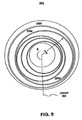
- FIG. 9 is a plan view of an exemplary loop capacitive sensor pattern 900 in accordance with embodiments of the invention.
- sensor pattern 900 includes two sets of concentric loop patterns of three sensing elements 202d, 204d, and 206d having three phases which can be utilized as part of a two-dimensional capacitive sensor apparatus (e.g., 100), such as but not limited to, a touch screen and/or a touchpad.
- sensor pattern 900 can provide continuous two-dimensional positioning information that has sensing elements with varying width and no crossovers.
- the sensor pattern 900 can be utilized in any manner similar to that described herein, but is not limited to such.
- each of the sensing elements 202d, 204d, and 206d has varying width and form a substantially circular (or loop) pattern
- a loop pattern may include any closed loop sensor pattern shape (e.g., circle, square, rectangle, triangle, polygon, etc.), radial arc sensor pattern, a semi-circle sensor pattern, and/or any sensor pattern that is not substantially in a straight line.
- the sensing elements 202d, 204d, and 206d are not required to overlap each other in order to determine an angular position ⁇ of an object relative to the substantially circular pattern (e.g., loop) in a two-dimensional space.
- the angular position ⁇ starts at an origin 902 which can be located anywhere associated with sensor pattern 900.
- the sensing elements 202d, 204d, and 206d provide a cumulative output signal that is substantially constant at different locations along the traces 202d, 204d, and 206d.
- the sensing elements 202d, 204d, and 206d can each include a conductive trace. Furthermore, each set of sensing elements (e.g., 202d, 204d, and 206d) can be used for determining a radial position "R" of the object relative to the loop in the two-dimensional space.
- each of the sensing elements (e.g., 202d, 204d, and 206d) of the sensor pattern 900 can be individually coupled with sensing circuitry 110 ( Figure 1 ) utilizing conductive coupling traces 104 and/or 106.
- the sensor pattern 900 can be utilized to form the sensing region 108.
- sensor pattern 900 can provide positioning information along the angular position ⁇ and the radial position "R".
- all similar sensing elements (e.g.; 202d) of sensor pattern 900 can be coupled together and coupled with sensing circuitry 110 ( Figure 1 ) utilizing conductive coupling traces 104 and/or 106.
- the sensor pattern 900 can provide positioning information to the sensing circuitry corresponding to the angular position ⁇ , but not of the radial position "R". It is understood that the radial position "R" can be determined in any manner similar to the way the second axis position can be determined, as described herein.
- sensor pattern 900 can be implemented with a greater or fewer number of sensing elements than shown within the present embodiment.
- sensor pattern 900 can be implemented with a single set of sensing elements 202d, 204d, and 206d.
- sensor pattern 900 can be implemented with multiple sets of sensing elements 202d, 204d, and 206d.
- Sensor pattern 900 and its sensing elements can be implemented in any manner similar to that described herein, but is not limited to such.
- each set of the sensing elements (e.g., 202d, 204d, and 206d) of sensor pattern 900 can operate in any manner similar to that described herein in order to provide the positioning information corresponding to the angular position ⁇ of an object (e.g., a user's finger, a probe, a stylus, and the like) in relation to sensor pattern 900.
- each set of the signals associated with a set of sensing elements (e.g., 202d, 204d, and 206d) can be utilized to determine the phase angle ⁇ , in a manner similar to that described herein with reference to Figures 2 and 4 . It is noted that once the phase angle ⁇ has been determined, it may be converted into a geometric position angle ⁇ relative to the origin 902. In this manner, the angular position ⁇ of an object is determined relative to sensor pattern 900.
- “coarse” or “fine” waveform patterns may have wavelengths that differ from the circumference of the loop sensor.
- FIG 10 is a plan view of an exemplary loop capacitive sensor pattern 1000 in accordance with embodiments of the invention.
- sensor pattern 1000 includes two sets of concentric loop patterns of four sensing elements 202e, 204e, 206e, and 1002 having four phases which can be utilized as part of a two-dimensional capacitive sensor apparatus (e.g., 100), such as but not limited to, a touch screen and/or a touchpad.
- sensor pattern 1000 can provide continuous two-dimensional positioning information that has sensing elements with varying width and no crossovers.
- the sensor pattern 1000 can be utilized in any manner similar to that described herein, but is not limited to such.
- each of the sensing elements 202e, 204e, 206e, and 1002 has varying width and form a substantially circular (or ioop) pattern. It is noted that sensing element 1002 can operate and be implemented in any manner similar to that described herein with reference to a sensing element.
- a loop pattern can include any closed loop sensor pattern shape (e.g., circle, square, rectangle, triangle, polygon, etc.), radial arc sensor pattern, a semi-circle sensor pattern, and/or any sensor pattern that is not substantially in a straight line.
- the sensing elements 202e, 204e, 206e, and 1002 are not required to overlap each other in order to determine an angular position ⁇ of an object relative to the substantially circular pattern (e.g., loop) in two-dimensional space.
- the angular position ⁇ starts at an origin 1004 which can be located anywhere associated with sensor pattern 1000.
- the sensing elements 202e, 204e, 206e, and 1002 provide a cumulative output signal that is substantially constant at different locations along the traces 202e, 204e, 206e, and 1002.
- the sensing elements 202e, 204e, 206e, and 1002 can each include a non-conductive region formed by two or more adjacent elements. Additionally, the sensing elements 202e, 204e, 206e, and 1002 can each include a conductive trace. Furthermore, each set of sensing elements (e.g., 202e, 204e, 206e, and 1002) can also be used for determining a radial position "R" of the object relative to the pattern 1000 in the two-dimensional space.
- each of the sensing elements (e.g., 202e, 204e, 206e, and 1002) of the sensor pattern 1000 can be individually coupled with sensing circuitry 110 ( Figure 1 ) utilizing conductive coupling traces 104 and/or 106.
- the sensor pattern 800 can be utilized to form the sensing region 108.
- sensor pattern 1000 can provide positioning information along the angular position ⁇ and the radial position "R".
- all similar sensing elements (e.g., 202e) of sensor pattern 1000 can be coupled together and coupled with sensing circuitry 110 ( Figure 1 ) utilizing conductive coupling traces 104 and/or 106.
- the sensor pattern 1000 can provide positioning information to the sensing circuitry corresponding to the angular position ⁇ , but hot of the radial position "R". It is understood that the radial position "R" can be determined in any manner similar to the way the second axis position can be determined, as described herein.
- sensor pattern 1000 can be implemented with a greater or fewer number of sensing elements than shown within the present embodiment. Sensor pattern 1000 and its sensing elements can be implemented in any manner similar to that described herein, but is not limited to such.
- each set of the sensing elements (e.g., 202e, 204e, 206e, and 1002) of sensor pattern 1000 can operate in any manner similar to that described herein in order to provide the positioning information corresponding to the angular position ⁇ of an object (e.g., a user's finger, a probe, a stylus, and the like) in relation to sensor pattern 1000.
- each set of the signals associated with a set of sensing elements e.g., 202e, 204e, 206e, and 1002 can be utilized to determine the phase angle ⁇ , in a manner similar to that as described herein with reference to Figures 2 and 4 .
- the phase angle ⁇ Once the phase angle ⁇ has been determined, it may be converted into a geometric position angle ⁇ , relative to the origin 1004. In this manner, the angular position ⁇ of an object relative to sensor pattern 1000 is determined.
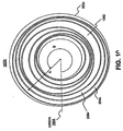
- FIG 11 is a plan view of an exemplary loop capacitive sensor pattern 1100 in accordance with embodiments of the invention.
- sensor pattern 1100 includes substantially "fixed" width sensing elements 1104, 1106, and 1108 along with four sets of concentric loop patterns of three sensing elements 202f, 204f, and 206f having three phases which can be utilized as part of a two-dimensional capacitive sensor apparatus (e.g., 100), such as but not limited to, a touch screen and/or a touchpad.
- sensor pattern 1100 can provide continuous two-dimensional positioning information that includes sensing elements with varying width and no crossovers.
- the sensor pattern 1100 can be utilized in any manner similar to that described herein, but is not limited to such.
- Each of the "fixed" width sensing elements 1104, 1106, and 1108 of sensor pattern 1100 can be individually coupled with sensing circuitry 110 ( Figure 1 ) utilizing conductive coupling traces 104 and/or 106. When coupled in this manner, sensing elements 1104, 1106, and 1108 can be utilized to provide positioning information to the sensing circuitry 110 associated with the radial position "R" of an object (e.g., a user's finger, a probe, a stylus, and the like) in relation to sensor pattern 1100. Additionally, each of the similar sensing elements of the four sets of sensing elements 202f, 204f, and 206f can be coupled together and coupled with sensing circuitry 110 ( Figure 1 ) utilizing conductive coupling traces 104 and/or 106. When coupled in this .manner, the four sets of sensing elements 202f, 204f, and 206f can provide positioning information to the sensing circuitry 110 corresponding to the angular position ⁇ of the object relative to an origin 1102.
- the constant width sensing elements 1104, 1106, and 1108 of Figure 11 can provide radial position "R" information to the sensing circuitry corresponding to the object while the four sets of sensing elements 202f, 204f, and 206f can provide angular position ⁇ information to the sensing circuitry associated with the sensor.
- each of the "fixed" width sensing elements 1104, 1106, and 1108 of sensor pattern 1100 are implemented with a width that is substantially fixed or constant. It is understood that the radial position "R" of sensor pattern 1100 can be determined in any manner similar to the way the second axis position can be determined, as described herein. The origin 1102 can be located anywhere with respect to sensor pattern 1100.
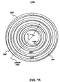
- FIG 12 is a plan view of an exemplary loop capacitive sensor pattern 1200 in accordance with embodiments of the invention.
- sensor pattern 1200 includes two sets of non-concentric loop patterns of three sensing elements 202g, 204g, and 206g having three phases which can be utilized as part of a two-dimensional capacitive sensor apparatus (e.g., 100), such as but not limited to, a touch screen and/or a touchpad.
- sensor pattern 1200 can provide continuous two-dimensional positioning information that has sensing elements with varying width and no crossovers.
- the sensor pattern 1200 can be utilized in any manner similar to that described herein, but is not limited to such.
- sensor pattern 1200 can operate in any manner similar to sensor pattern 900 of Figure 9 . Furthermore, it is appreciated that the sum of the widths of any three adjacent traces (or sensing elements) of sensor pattern 1200 can be implemented as a substantial constant width. The sensor pattern 1200 can be implemented with a greater or fewer number of sensing elements than shown within the present embodiment. Sensor pattern 1200 and its sensing elements can be implemented in any manner similar to that described herein, but is not limited to such.
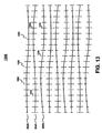
- FIG 13 is a plan view of an exemplary "fishbone" capacitive sensor pattern 1300 in accordance with embodiments of the invention.
- sensor pattern 1300 includes three repeated patterns of sensing elements 202h, 204h, and 206h having three phases which can be utilized as part of a two-dimensional capacitive sensor apparatus (e.g., 100), such as but not limited to, a touch screen and/or a touchpad.
- sensor pattern 1300 can provide two-dimensional positioning information that has substantially parallel traces (or sensing elements) with no crossovers.
- the sensor pattern 1300 can be utilized in any manner similar to that described herein with reference to Figures 2 and 4 . Additionally, sensor pattern 1300 can be utilized in any manner similar to that described herein, but is not limited to such.
- sensing element 202h includes a plurality of extensions 1302 that are substantially parallel to each other and are substantially perpendicular (or non-parallel) to a first axis of sensing element 202h. It is noted that the plurality of extensions 1302 cumulatively defines an envelope the shape of a first waveform.
- the sensing element 204h includes a plurality of extensions 1304 that are substantially parallel to each other and are substantially perpendicular (or non-parallel) to the first axis of sensing element 204h. It is understood that the plurality of extensions 1304 cumulatively defines an envelope the shape of a second waveform.
- the sensing element 206h includes a plurality of extensions 1306 that are substantially parallel to each other and are substantially perpendicular (or non-parallel) to the first axis of sensing element 206h. It is appreciated that the plurality of extensions 1306 cumulatively defines an envelope the shape of a third waveform.
- the repeated sets of sensing elements 202h, 204h, and 206h can be used for determining a first location of an object (e.g., a user's finger, a probe, a stylus, and the like) in relation to sensor pattern 1300 along the first axis of a two-dimensional space. Furthermore, the repeated sets of sensing elements 202h, 204h, and 206h can be used for determining first and second locations of an object in relation to sensor pattern 1300 along the first axis and a second axis of the two-dimensional space, wherein the second axis is substantially non-parallel (or substantially perpendicular) to the first axis.
- an object e.g., a user's finger, a probe, a stylus, and the like
- the repeated sets of sensing elements 202h, 204h, and 206h can be used for determining first and second locations of an object in relation to sensor pattern 1300 along the first axis and a second axis of the
- sensor pattern 1300 can operate in any manner similar to sensor pattern 500 of Figure 5 . Furthermore, it is appreciated that the sum of the widths of any three adjacent traces (or sensing elements) of sensor pattern 1300 can be implemented as a substantial constant width. The sensor pattern 1300 can be implemented with a greater or fewer number of sensing elements than shown within the present embodiment. Sensor pattern 1300 and its sensing elements can be implemented in any manner similar to that described herein, but is not limited to such.
- FIG 14 is a plan view of an exemplary "fishbone" capacitive sensor pattern 1400 in accordance witch embodiments of the invention.
- sensor pattern 1400 includes three repeated patterns of sensing elements 202i, 204i, and 206i having three phases which can be utilized as part of a two-dimensional capacitive sensor apparatus (e.g., 100), such as but not limited to, a touch screen and/or a touchpad.
- sensor pattern 1400 can provide two-dimensional positioning information that has substantially parallel traces (or sensing elements) with no crossovers.
- the sensor pattern 1400 can be utilized in any manner similar to that described herein with reference to Figures 2 and 4 .
- sensor pattern 1400 can be utilized in any manner similar to that described herein, but is not limited to such.
- sensing element 202i includes a plurality of extensions 1402 that are substantially parallel to each other and are substantially non-parallel to a first axis of sensing element 202i. It is noted that the plurality of extensions 1402 cumulatively defines an envelope the shape of a first waveform.
- the sensing element 204i includes a plurality of extensions 1404 that are substantially parallel to each other and are substantially non-parallel to the first axis of sensing element 204i. It is understood that the plurality of extensions 1404 cumulatively defines an envelope the shape of a second waveform.
- the sensing element 206i includes a plurality of extensions 1406 that are substantially parallel to each other and are substantially non-parallel to the first axis of sensing element 206i. It is appreciated that the plurality of extensions 1406 cumulatively defines an envelope the shape of a third waveform.
- the repeated sets of sensing elements 202i, 204i, and 206i can be used for determining a first location of an object (e.g., a user's finger, a probe, a stylus, and the like) in relation to sensor pattern 1400 along the first axis of a two-dimensional space. Furthermore, the repeated sets of sensing elements 202i, 204i, and 206i can be used for determining first and second locations of an object in relation to sensor pattern 1400 along the first axis and a second axis of the two-dimensional space, wherein the second axis is substantially non-parallel (or substantially perpendicular) to the first axis.
- an object e.g., a user's finger, a probe, a stylus, and the like
- the repeated sets of sensing elements 202i, 204i, and 206i can be used for determining first and second locations of an object in relation to sensor pattern 1400 along the first axis and a second axis of the
- sensor pattern 1400 can operate in any manner similar to sensor pattern 500 of Figure 5 . Furthermore, it is appreciated that the sum of the widths of any three adjacent traces (or sensing elements) of sensor pattern 1400 can be implemented as a substantial constant width.
- the sensor patterns 1400 can be implemented with a greater or fewer number of sensing elements than shown within the present embodiment. Sensor pattern 1400 and its sensing elements can be implemented in any manner similar to that described herein, but is not limited to such.
- second axis sensing elements having substantially constant width can be implemented as part of sensor patterns 1300 and/or 1400.
- second axis sensing elements can be incorporated with sensor patterns 1300 and/or 1400 in any manner similar to that described herein with reference to Figures 6 and 7 , but is not limited to such.
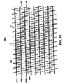
- FIG 15 is a plan view of an exemplary "fishbone" capacitive sensor pattern 1500 in accordance with embodiments of the invention.
- sensor pattern 1500 includes three repeated patterns of sensing elements 202j, 204j, and 206j having three phases which can be utilized as part of a two-dimensional capacitive sensor apparatus (e.g., 100), such as but not limited to, a touch screen and/or a touchpad.
- sensor pattern 1500 can provide two-dimensional positioning information that has substantially parallel traces (or sensing elements) with no crossovers.
- the sensor pattern 1500 can be utilized in any manner similar to that described herein with reference to Figures 2 and 4 , but is not limited to such.
- sensor pattern 1500 can be utilized in any manner similar to that described herein, but is not limited to such.
- sensing element 202j includes a plurality of extensions 1502 that are substantially parallel to each other and are substantially perpendicular to a first axis of sensing element 202j. It is noted that the plurality of extensions 1502 can each be implemented with a different width that slightly varies with its neighboring extension. As such, a first waveform is defined by the varying widths of the plurality of extensions 1502.
- the sensing element L 204j includes a plurality of extensions 1504 that are substantially parallel to each other and are substantially perpendicular to the first axis of sending element 204j. It is understood that the plurality of extensions 1504 can each be implemented with a different width that slightly varies with its neighboring extension.
- a second waveform is defined by the varying widths of the plurality of extensions 1504.
- the sensing element 206j includes a plurality of extensions 1506 that are substantially parallel to each other and are substantially perpendicular to the first axis of sensing element 206j. It is appreciated that the plurality of extensions 1506 can each be implemented with a different width that slightly varies with its neighboring extension. As such, a third waveform is defined by the varying widths of the plurality of extensions 1506.
- the plurality of extensions 1502 of sensing element 202j are interdigitated with the plurality of extensions 1504 of sensing element 204j.
- the plurality of extensions 1506 of sensing element 206j are interdigitated with the plurality of extensions 1504 of sensing element 204j.
- the repeated sets of sensing elements 202j, 204j, and 206j can be used for determining a first location of an object (e.g., a user's finger, a probe, a stylus, and the like) in relation to sensor pattern 1500 along the first axis of a two-dimensional space. Furthermore, the repeated sets of sensing elements 202j, 204j, and 206j can be used for determining first and second locations of an object in relation to sensor pattern 1500 along the first axis and a second axis of the two-dimensional space, wherein the second axis is substantially non-parallel (or substantially perpendicular) to the first axis.
- an object e.g., a user's finger, a probe, a stylus, and the like
- the repeated sets of sensing elements 202j, 204j, and 206j can be used for determining first and second locations of an object in relation to sensor pattern 1500 along the first axis and a second axis of the two-dimensional
- sensor pattern 1500 can operate in any manner similar to sensor pattern 500 of Figure 5 . Additionally, the sensor pattern 1500 can be implemented with a greater or fewer number of sensing elements than shown within the present embodiment. Sensor pattern 1500 and its sensing elements can be implemented in any manner similar to that described herein, but is not limited to such.
- FIG 16 is a plan view of an exemplary "fishbone" capacitive sensor pattern 1600 in accordance with embodiments of the invention.
- sensor pattern 1600 includes four repeated patterns of sensing elements 202k, 204k, and 206k having three phases which can be utilized as part of a two-dimensional capacitive sensor apparatus (e.g., 100), such as but not limited to, a touch screen and/or a touchpad.
- sensor pattern 1600 can provide two-dimensional positioning information that has substantially parallel traces (or sensing elements) with no crossovers.
- the sensor pattern 1600 can be utilized in any manner similar to that described herein with reference to Figures 2 and 4 , but is not limited to such.
- sensor pattern 1600 can be utilized in any manner similar to that described herein, but is not limited to such.
- sensing element 202k includes a plurality of extensions 1602 that are substantially parallel to each other and are substantially non-parallel to a first axis of sensing element 202k. It is noted that the plurality of extensions 1602 can each be implemented with a different width that slightly varies with its neighboring extension. As such, a first waveform is defined by the varying widths of the plurality of extensions 1602.
- the sensing element 204k includes a plurality of extensions 1604 that are substantially parallel to each other and are substantially non-parallel to the first axis of sensing element 204k. It is understood that the plurality of extensions 1604 can each be implemented with a different width that slightly varies with its neighboring extension.
- a second waveform is defined by the varying widths of the plurality of extensions 1604.
- the sensing element 206k includes a plurality of extensions 1606 that are substantially parallel to each other and are substantially non-parallel to the first axis of sensing element 206k. It is appreciated that the plurality of extensions 1606 can each be implemented with a different width that slightly varies with its neighboring extension. As such, a third waveform is defined by the varying widths of the plurality of extensions 1 606.
- the plurality of extensions 1602 of sensing element 202k are interdigitated with the plurality of extensions 1604 of sensing element 204k. Furthermore, the plurality of extensions 1606 of sensing element 206k are interdigitated with the plurality of extensions 1604 of sensing element 204k.
- the repeated sets of sensing elements 202k, 204k, and 206k can be used for determining a first location of an object (e.g., a user's finger, a probe, a stylus, and the like) in relation to sensor pattern 1600 along the first axis of a two-dimensional space. Additionally, the repeated sets of sensing elements 202k, 204k, and 206k can be used for determining first and second locations of an object in relation to sensor pattern 1600 along the first axis and a second axis of the two-dimensional space, wherein the second axis is substantially non-parallel (or substantially perpendicular) to the first axis.
- an object e.g., a user's finger, a probe, a stylus, and the like
- the repeated sets of sensing elements 202k, 204k, and 206k can be used for determining first and second locations of an object in relation to sensor pattern 1600 along the first axis and a second axis of the two-dimensional
- sensor pattern 1600 can operate in any manner similar to sensor pattern 500 of Figure 5 . Furthermore, the sensor pattern 1600 can be implemented with a greater or fewer number of sensing elements than shown within the present embodiment. Sensor pattern 1600 and its sensing elements can be implemented in any manner similar to that described herein, but is not limited to such.
- sensor patterns 500-1600 may each be operated with very few sensor channels. This can offer substantial cost savings if it there is a desire to use a low pin-count package, or build a simplified sensor ASIC (application-specific integrated circuit) for a capacitive sensor device or apparatus.
- ASIC application-specific integrated circuit
- sensor patterns 200, 300, and 500-1600 can each provide a capacitive sensing geometry that does not induce signal to noise ratio concerns. Additionally, sensor patterns 500-1600 may each be used to detect objects on either side of the substrate onto which it is fabricated. To prevent detection of signals of noise from one side of the substrate, a ground plane or a driven shield conductor may be utilized with each of sensor patterns 500-1600 to shield that side.
- the sensing elements of sensor patterns 200, 300, and 500-1600 can each include a non-conductive region formed by two or more adjacent sensing elements.
Landscapes
- Engineering & Computer Science (AREA)
- General Engineering & Computer Science (AREA)
- Theoretical Computer Science (AREA)
- Physics & Mathematics (AREA)
- General Physics & Mathematics (AREA)
- Human Computer Interaction (AREA)
- Quality & Reliability (AREA)
- Measurement Of Length, Angles, Or The Like Using Electric Or Magnetic Means (AREA)
- Position Input By Displaying (AREA)
- Measurement Of Resistance Or Impedance (AREA)
- Testing Or Measuring Of Semiconductors Or The Like (AREA)
Abstract
Description
- Conventional computing devices provide several ways for enabling a user to input a choice or a selection. For example, a user can use one or more keys of an alphanumeric keyboard communicatively connected to the computing device in order to indicate a choice or selection. Additionally, a user can use a cursor control device communicatively connected to the computing device to indicate a choice. Also, a user can use a microphone communicatively connected to the computing device to audibly indicate a particular selection. Moreover, touch sensing technology can be used to provide an input selection to a computing device or other electronic device.
- Within the broad category of touch sensing technology there exist capacitive sensing touch screens. Among conventional capacitive sensing touch screens, there are different sensing technologies. For example, one sensing technology involves the use of sensing electrodes formed in triangular shapes wherein the direction of each triangle point alternates. However, there are disadvantages associated with this technique. For instance, one of the disadvantages is that as a finger (or object) moves towards the wide end of a first triangular shaped electrode and the narrow point of a second triangular shaped electrode, the narrow point electrode does not provide a quality signal because of its inherent signal to noise ratio. As such, this can be referred to as sensing geometry that induces signal to noise ratio concerns.
- Another sensing technology uses a grid of conductive elements that cross over one another. While this design offers ease of signal interpretation, it also has the disadvantage of higher manufacturing cost. A further disadvantage affects multiple-layer sensors, as each layer degrades optical clarity of a capacitive sensing touch screen.
- The present invention may address one or more of the above mentioned issues.
- One embodiment in accordance with the invention includes a two-dimensional capacitive sensor apparatus. The two-dimensional capacitive sensor can include a first sensing element having varying width, a second sensing element having varying width, and a third sensing element having varying width. Additionally, the first sensing element, second sensing element, and third sensing element are substantially parallel to a first axis. Furthermore, each of the first sensing element, second sensing element, and third sensing element can be located such that they are not required to overlap each other to determine a first location along the first axis of a two-dimensional space. Moreover, the first sensing element, second sensing element, and third sensing element can have a cumulative width that is substantially constant.
- The present application discloses the following concepts:
-
Concept 1. A two-dimensional capacitive sensor apparatus comprising: a first sensing element having varying width; and a second sensing element having varying width, wherein said first sensing element and second sensing element are conductive and form a loop, each of said first sensing element and said second sensing element is located such that said first sensing element and second sensing element are not required to overlap each other to determine an angular position of an object relative to said loop in a two-dimensional space. - Concept 2. The two-dimensional capacitive sensor apparatus of
Concept 1, wherein: said first sensing element comprises a first waveform; and said second sensing element comprises a second waveform. - Concept 3. The two-dimensional capacitive sensor apparatus of Concept 2, wherein: said first sensing element comprises a first phase; and said second sensing element comprises a second phase different from said first phase.
-
Concept 4. The apparatus ofconcept 1 further comprising: a third sensing element having varying width, wherein said first sensing element, second sensing element, and third sensing element form a substantially circular pattern, and are located such that said first sensing element, second sensing element, and third sensing element are not required to overlap each other to determine an angular position of an object relative to said substantially circular pattern in a two-dimensional space, wherein said first sensing element, second sensing element, and third sensing element provide a cumulative output signal that is substantially constant at different locations along said substantially circular pattern. - Concept 5. The two-dimensional capacitive sensor apparatus of
Concept 4, wherein: said first sensing element comprises a waveform; said second sensing element comprises a waveform that is offset from said waveform of said first sensing element by 2π/3 radians; and said third sensing element comprises a waveform that is offset from said waveform of said first sensing element by 2π/3 radians. - Concept 6. The two-dimensional capacitive sensor apparatus of
Concept 4, wherein said angular position is determined using a first sensing element signal, a second sensing element signal, and a third sensing element signal. - Concept 7. The two-dimensional capacitive sensor apparatus of Concept 6, wherein said angular position is determined using a trigonometric function.
- Concept 8. A two-dimensional capacitive sensor apparatus which does not require overlapping sensing elements comprising: a first sensing element that is conductive; a second sensing element that is conductive; and a third sensing element that is conductive; wherein the shape of said second sensing element is defined by the shape of said first sensing element and the shape of said third sensing element, wherein said first sensing element second sensing element, and third sensing element form a loop for determining an angular location of an object relative to said loop within a two-dimensional space.
- Concept 9. The two-dimensional capacitive sensor apparatus of
Concept - Concept 10. A two-dimensional capacitive sensor apparatus comprising: a first sensing element having varying width; a second sensing element having varying width; and a third sensing element having varying width, wherein said first sensing element, second sensing element, and third sensing element are conductive and substantially parallel to a first axis, each of said first sensing element, second sensing element, and third sensing element are located such that said first sensing element, second sensing element, and third sensing element are not required to overlap each other to determine a first location along said first axis of a two-dimensional space, and wherein said first sensing element, second sensing element, and third sensing element have a cumulative width that is substantially constant.
- Concept 11. The two-dimensional capacitive sensor apparatus of Concept 10, wherein said first sensing element, second sensing element, and third sensing element are used for determining a second location along a second axis substantially perpendicular to said first axis.
- Concept 12. The two-dimensional capacitive sensor apparatus of Concept 10, wherein: said first sensing element comprises a sine (θ) waveform; said second sensing element comprises a waveform offset from said sine (θ) waveform; and said third sensing element comprises a waveform offset from said sine (θ) waveform.
- Concept 13. The two-dimensional capacitive sensor apparatus of Concept 10, wherein said first location along said first axis is determined using a first sensing element signal, a second sensing element signal, and a third sensing element signal.
- Concept 14. The two-dimensional capacitive sensor apparatus of Concept 10, wherein said first location along said first axis is determined using a trigonometric function.
- Concept 15. The two-dimensional capacitive sensor apparatus of Concept 10, further comprising: a fourth sensing element utilized to determine a second location along a second axis that is substantially perpendicular to said first axis, said fourth sensing element being substantially parallel to said first axis.
- Concept 16. The two-dimensional capacitive sensor apparatus of Concept 10, further comprising: a fourth sensing element having varying width; a fifth sensing element having varying width; and a sixth sensing element having varying width, wherein said fourth, fifth, and sixth sensing elements are substantially parallel to said first sensing element, and are located such that each does not require overlap of said first, second, third, fourth, fifth, and sixth sensing elements to determine said first location along said first axis.
- Concept 17. The two-dimensional capacitive sensor apparatus of Concept 16, wherein said first, second, third, fourth, fifth, and sixth sensing elements are used to determine a second position along a second axis, not parallel to said first axis.
- Concept 18. The two-dimensional capacitive sensor apparatus of Concept 16, wherein said first, second, and third sensing elements each comprises a first sinusoidal waveform; and said fourth, fifth, and sixth sensing elements each comprises a second sinusoidal waveform.
- Concept 19. The two-dimensional capacitive sensor apparatus of Concept 18, wherein, first sinusoidal waveform has a lower frequency than said second sinusoidal waveform.
- Concept 20. The two-dimensional capacitive sensor apparatus of Concept 10, wherein said first, second, and third sensing elements are utilized as part of a capacitive touch screen device or capacitive touch pad device.
- Concept 21. A two-dimensional capacitive sensor apparatus comprising: a first sensing element having varying width and is conductive; a second sensing element having varying width and is conductive; and a third sensing element having varying width and is conductive, wherein said first sensing element, second sensing element, and third sensing element are substantially parallel to a first axis and are located such that said first sensing element, second sensing element, and third sensing element are not required to overlap each other to determine a first location along said first axis of a two-dimensional space, wherein said first sensing element, second sensing element, and third sensing element provide a cumulative output signal that is substantially constant at different locations along said first sensing element, second sensing element, and third sensing element.
- Concept 22. The two-dimensional capacitive sensor apparatus of Concept 21, wherein said first sensing element, second sensing element, and third sensing element are used for determining a second location along a second axis, substantially perpendicular to said first axis.
- Concept 23. The two-dimensional capacitive sensor apparatus of Concept 21, wherein said first location along said first axis is determined using a first sensing element signal, a second sensing element signal, a third sensing element signal, and a trigonometric function.
- Concept 24. The two-dimensional capacitive sensor apparatus of Concept 21, further comprising: a fourth sensing element utilized to determine a second location along a second axis that is non-parallel to said first axis, said fourth sensing element substantially parallel to said third sensing element.
- Concept 25. A two-dimensional capacitive sensor apparatus that does not require overlapping sensing elements comprising: a first conductive trace including a first plurality of extensions that are substantially parallel to each other and are substantially non-parallel to a first axis of said first conductive trace, said first plurality of extensions cumulatively defines an envelope in the shape of a first waveform; a second conductive trace including a second plurality of extensions that are substantially parallel to each other and are substantially non-parallel to said first axis of said second conductive trace, said second plurality of extensions cumulatively defines an envelope in the shape of a second waveform; and a third conductive trace including a third plurality of extensions that are substantially parallel to each other and are substantially non-parallel to said first axis of said third conductive trace, said third plurality of extensions cumulatively defines an envelope in the shape of a third waveform, wherein said first, second, and third conductive traces are used for determining a first location along said first axis of a two-dimensional space.
- Concept 26. The two-dimensional capacitive sensor apparatus of Concept 25, wherein said first plurality of extensions and said second plurality of extensions are interdigitated.
- Concept 27. The two-dimensional capacitive sensor apparatus of Concept 26, wherein said second plurality of extensions and said third plurality of extensions are interdigitated.
- Concept 28. A portable electronic device comprising: a two-dimensional capacitive sensor; and a processor coupled with said two-dimensional capacitive sensor; wherein said two-dimensional capacitive sensor comprises: a first sensing element having varying width; a second sensing element having varying width; and a third sensing element having varying width, wherein said first sensing element, second sensing element, and third sensing element are each conductive and substantially parallel to a first axis, each of said first sensing element, second sensing element, and third sensing element is located such that said first sensing element, second sensing element, and third sensing element are not required to overlap each other to determine a first location along said first axis of a two-dimensional space, wherein said first sensing element, second sensing element, and third sensing element have a cumulative width that is substantially constant.
- Concept 29. the portable electronic device of Concept 28, wherein said first sensing element, second sensing element, and third sensing element are used for determining a second location along a second axis not parallel to said first axis.
- Concept 30. The portable electronic device of
Concept 4, 8, 10, 21 or 28, wherein: said first sensing element comprises a first waveform; said second sensing element comprises a second waveform; and said third sensing element comprises a third waveform. - Concept 31. The portable electronic device of Concept 21 or 30, wherein: said first sensing element comprises a first phase; said second sensing element comprises a second phase; and said third sensing element comprises a third phase.
- Concept 32. The portable electronic device of Concept 28, wherein: said first sensing element comprises a sine (θ) waveform; said second sensing element comprises a sine (θ) waveform shifted from said sine (θ) waveform of said first sensing element by 2π/3 radians; and said third sensing element comprises a sine (θ) waveform shifted from said sine (θ) waveform of said first sensing element by 2π/3 radians.
- Concept 33. The portable electronic device of Concept 28, wherein said first location along said first axis is determined using a; first sensing element signal, a second sensing element signal, and a third sensing element signal.
- Concept 34. The portable electronic device of Concept 28, when in said first location along said first axis is determined using a trigonometric function.
- Concept 35. The portable electronic device of Concept 28, further comprising: a fourth sensing element utilized to determine a second location along a second axis that is substantially perpendicular to said first axis, said fourth sensing element being substantially parallel to said first axis.
- Concept 36. A portable electronic device comprising: a two-dimensional capacitive sensor; and a processor coupled with said two-dimensional capacitive sensor; wherein said two-dimensional capacitive sensor comprises: a first sensing element having varying width; a second sensing element having varying width; and a third sensing element having varying width, wherein said first sensing element, second sensing element, and third sensing element are conductive and disposed along a loop, each of said first sensing element, second sensing element, and third sensing element is located such that said first sensing element, second sensing element, and third sensing element are not required to overlap each other to determine an angular location of an object relative to said loop within a two-dimensional space, wherein said first sensing element, second sensing element, and third sensing element have a cumulative width that is substantially constant.
- Concept 37 The portable electronic device of Concept 36, wherein said first sensing element, said second sensing element, and third sensing element are used for determining a radial position of said object relative to said loop in said two-dimensional space.
- Concept 38. The portable electronic device of Concept 36, wherein said first sensing element, second sensing element, and third sensing element provide a cumulative output signal that is substantially constant at different locations along said first sensing element, second sensing element, and third sensing element.
- Concept 39. The portable electronic device of Concept 36, wherein: said first sensing element comprises a phase; said second sensing element comprises a phase different from said phase of said first sensing element; and said third sensing element comprises a phase different from said phase of said first sensing element.
- Concept 40. A capacftive sensor device comprising: a substrate; a first conductive trace having varying width and disposed above said substrate; a second conductive trace having varying width and disposed above said substrate; and a third conductive trace having varying width and disposed above said substrate, wherein said first, second, and third conductive traces are substantially parallel to a first axis and are located such that each does not require overlap of said first, second, and third conductive traces to determine a first axis location.
- Concept 41. The capacitive sensor device of Concept 40, wherein: said first conductive trace comprises a first waveform; said second conductive trace comprises a second waveform; and said third conductive trace comprises a third waveform.
- Concept 42. The capacitive sensor device of Concept 41 wherein: said first conductive trace comprises a first phase; said second conductive trace comprises a second phase; and said third conductive trace comprises a third phase.
- Concept 43. The capacitive sensor device of Concept 40, wherein said first, second, and third conductive traces have a cumulative width that is substantially constant.
- Concept 44. The capacitive sensor device of Concept 40, wherein said first axis location is determined using a first conductive trace signal, a second conductive trace signal, and a third conductive trace signal.
- Concept 45. The capacitive sensor device of Concept 40, further comprising: a fourth conductive trace utilized to determine a second axis location, that is not parallel to said first axis location, said fourth conductive trace is not parallel to said first axis.
- Concept 46. The capacitive sensor device of Concept 40, wherein said first, second, and third conductive traces are utilized to determine a second axis location that is not parallel to said first axis.
- Concept 47. A two-dimensional capacitive sensor apparatus comprising: a first sensing element having varying width; a second sensing element having varying width; and a third sensing element haying varying width, wherein said first sensing element, second sensing element, and third sensing element are conductive and form a curved path, each of said first sensing element, second sensing element, and third sensing element is located such that said first sensing element, second sensing element, and third sensing element are not required to overlap each other to determine a radial location along said curved path of a two- dimensional space, wherein said first sensing element, second sensing element, and third sensing element have a cumulative width that is substantially constant.
- Concept 48. The portable electronic device of Concept 47, wherein said first sensing element, said second sensing element, and third sensing element are used for determining an angular position of said object relative to said curved path in said two-dimensional space.
- Concept 49. The portable electronic device of Concept 47, wherein said first sensing element, second sensing element, and third sensing element provide a cumulative output signal that is substantially constant at different locations along said first sensing element, second sensing element, and third sensing element.
- Concept 50. The portable electronic device of Concept 36 or 47, wherein: said first sensing element comprises a waveform; said second sensing element comprises a waveform; and said third sensing element comprises a waveform.
- Concept 51. The portable electronic device of Concept 50, wherein: said first sensing element comprises a phase; said second sensing element comprises a phase different from said phase of said first sensing element; and said third sensing element comprises a phase different from said phase of said first sensing element.
- Concept 52. The portable electronic device or capacitive sensor of
Concept 1, 8, 36, 42 or 47, wherein said sensing elements each comprises a sinusoidal waveform. -
-
Figure 1 is an exemplary capacitive touch screen device that can be implemented to include one or more embodiments of the invention. -
Figure 2 illustrates an exemplary capacitive sensor pattern in accordance with embodiments of the invention. -
Figure 3 illustrates another exemplary capacitive sensor pattern in accordance with embodiments of the invention. -
Figure 4 illustrates an exemplary signal strength chart along with its conversion into polar coordinates in accordance with embodiments of the invention. -
Figure 5 illustrates yet another exemplary capacitive sensor pattern in accordance with embodiments of the invention. -
Figure 6 illustrates still another exemplary capacitive sensor pattern in accordance with embodiments of the invention. -
Figure 7 illustrates another exemplary capacitive sensor pattern in accordance with embodiments of the invention. -
Figure 8 illustrates yet another exemplary capacitive sensor pattern in accordance with embodiments of the invention. -
Figure 9 illustrates an exemplary loop capacitive sensor pattern in accordance with embodiments of the invention. -
Figure 10 illustrates another exemplary loop capacitive sensor pattern in accordance with embodiments of the invention. -
Figure 11 illustrates yet another exemplary loop capacitive sensor pattern in accordance with embodiments of the invention. -
Figure 12 illustrates still exemplary loop capacitive sensor pattern in accordance with embodiments of the invention. -
Figure 13 illustrates an exemplary "fishbone" capacitive sensor pattern in accordance with embodiments of the invention. -
Figure 14 illustrates another exemplary "fishbone" capacitive sensor pattern in accordance with embodiments of the invention. -
Figure 15 illustrates yet another exemplary "fishbone" capacitive sensor pattern in accordance with embodiments of the invention. -
Figure 16 illustrates still another exemplary "fishbone" capacitive sensor pattern in accordance with embodiments of the invention. - The drawings referred to in this description should not be understood as being drawn to scale except if specifically noted.
- Reference will now be made in detail to embodiments of the invention, examples of which are illustrated in the accompanying drawings. While the invention will be described in conjunction with embodiments, it will be understood that they are not intended to limit the invention to these embodiments. On the contrary, the invention is intended to cover alternatives, modifications and equivalents, which may be included within the spirit and scope of the invention as defined by the appended claims. Furthermore, in the following detailed description of the present invention, numerous specific details are set forth in order to provide a thorough understanding of the present invention. However, it will be obvious to one of ordinary skill in the art that the present invention may be practiced without these specific details. In other instances, well known methods, procedures, components, and circuits have not been described in detail as not to unnecessarily obscure aspects of the present invention.
-
Figure 1 is a plan view of an exemplary two-dimensionalcapacitive sensor apparatus 100 that can be implemented to include one or more embodiments of the present invention. Thecapacitive sensor apparatus 100 can be utilized to communicate user input (e.g., using a user's finger or a probe) to a computing device or other electronic device. For example,capacitive sensor apparatus 100 can be implemented as a capacitive touch screen device that can be placed over an underlying image or an information display device (not shown). In this manner, a user would view the underlying image or information display by looking through the substantiallytransparent sensing region 108 ofcapacitive sensor apparatus 100 as shown. It is noted that one or more embodiments in accordance with the present invention can be incorporated with a capacitive touch screen device similar tocapacitive sensor apparatus 100. - The
capacitive sensor apparatus 100 when implemented as a touch screen can include a substantiallytransparent substrate 102 having a first set of conductive coupling traces 104 and a second set of conductive coupling traces 106 patterned (or formed) thereon. Conductive coupling traces 104 and/or 106 can be utilized for coupling any sensing elements (not shown) or conductive traces that would form asensing region 108 withsensing circuitry 110 thereby enabling the operation ofcapacitive sensor apparatus 100. Conductive coupling traces 104 and 106 may each include one or more conductive coupling elements or traces. It is noted that embodiments of sensing element patterns in accordance with the invention are described herein which can be implemented to formsensing region 108. - Within
Figure 1 , thecapacitive sensor apparatus 100 can also be implemented as a capacitive touchpad device. For example,substrate 102 ofcapacitive sensor apparatus 100 can be implemented with, but is not limited to, one or more opaque materials that are utilized as a substrate for a capacitive touchpad device. -
Figure 2 is a plan view of an exemplarycapacitive sensor pattern 200 in accordance with embodiments of the invention. Specifically,sensor pattern 200 includes sensingelements sensor pattern 200 provides positioning information from a sensor pattern that has substantially parallel traces (or elements) with no crossovers. The positioning information can be derived from which sensing element detects an object (e.g., a user's finger, a probe, and the like), and the proportional strength of the signals on sensingelements - Specifically, sensing
elements sensing elements sensing elements sensing element sensing element traces - Within
Figure 2 , the phases oftraces traces sensing elements elements sensing elements sensing elements sensor pattern 200. It is noted that thesensing elements - The shape and phase of the
sensing elements sensing element 202 is substantially equal to sin e, then the waveform shape ofsensing element 204 may be substantially equal to sin θ + 120 degrees, while the waveform shape ofsensing element 206 may be substantially equal to sin θ + 240 degrees. Alternatively, the waveforms of sensingelements sensing element 202 by 2π/3 radians. However, it is understood that the phase and shape of the waveform of sensingelements - There are a wide variety of ways in accordance with the present embodiment for determining a location (or position) of an object in relation to the length of
sensor pattern 200 using signals output by sensingelements Figure 4 illustrates an exemplarysignal strength chart 402 along with its conversion into polar coordinates in accordance with embodiments of the invention. For example, suppose signal "A" is associated with sensing element 202 (Figure 2 ), signal "B" is associated withsensing element 204, and signal "C" is associated withsensing element 206. As such, based on the signal strength shown withinchart 402, it can be determined that the object is located alongsensor 200 wheresensing trace 204 is the widest, thesensing trace 202 is the second widest, and thesensing trace 206 is the third widest. Therefore, within this example, the object is located near the right-hand end ofsensor pattern 200. - More specifically, given signal "A" corresponds to
sensing element 202, signal "B" corresponds tosensing element 204, and signal "C" corresponds tosensing element 206, as mentioned above. And further suppose that sensing elements (or traces) 202, 204, and 206 have been observed to give values A0, B0, and C0, respectively, when no object is present ornear sensor pattern 200. As such, let a = A - A0, b = B - B0, and c = C - C0. Therefore, determination of the polar coordinates "h", "r", and angle θ that are associated with signals A, B, and C can be performed. - Within
Figure 4 , it is noted that the value of "h" corresponds to the height of the center of acircle 404 upon which points 406, 408, and 410 can be located. Thepoints circle 404. The value of angle θ can be used to indicate the linear location (or position) of an object in relationship to the length ofsensor pattern 200. Specifically, the value of height "h" can be determined by using the following relationship:


sensor pattern 200 from one of its end points. For example, each degree of angle θ may be equal to a specific distance (e.g., a specific number of millimeters or inches) from one of the end points ofsensor pattern 200. Alternatively, a lookup table may be utilized to ascertain the distance that corresponds to the determined e. It is noted that the angle θ provides the location of the center of the object alongsensor pattern 200 while the "h" and the "r" can provide information regarding the size of the object. - One of the advantages of determining the position along the first axis (e.g., X axis) of
sensor pattern 200 in the manner described above is that common-mode noise has no effect on the determination of "r" and θ. - Within
Figure 4 , it is noted that angle θ can alternatively be determined utilizing the following relationships:


- The
sensing elements sensor pattern 200 can be fabricated with any conductive material on any insulating substrate (e.g., 102). For example, this may include conventional copper/fiberglass printed circuit construction, ITO patterned on glass, screen printed conductor patterned on plastic, and the like. It is noted that thesensor pattern 200 may be used to detect objects on either side of the substrate onto which it is fabricated. To prevent detection of signals of noise from one side of the substrate, a ground plane or a driven shield conductor may be utilized to shield that side. - There are advantages associated with the
sensor pattern 200 ofFigure 2 . For example, since the manufacture ofsensor pattern 200 involves one layer of conductive material, this reduces manufacturing costs relative to the two-layer X-Y grids often used in touchpads. Additionally, in the case of touch screens, doing all the fabrication using only one layer of conductive material eliminates low yield alignment steps. Furthermore, the optical properties of touch screens can also benefit from the use of only one layer of substantially transparent conductive material, such as indium tin oxide (ITO). - It is noted that
sensor pattern 200 can be implemented with a greater number of sensing elements than thesensing elements sensor pattern 200 is implemented with a greater number of sensing elements, the relationships described with reference toFigures 4 and2 would be modified accordingly in order to determine "h", "r", and θ. - Within
Figure 2 , it is understood that sensingelements sensor pattern 200 can individually be coupled with sensing circuitry 110 (Figure 1 ) utilizing conductive coupling traces 104 and/or 106. When coupled in this manner, thesensor pattern 200 can be utilized to form thesensing region 108. -
Figure 3 is a plan view of an exemplarycapacitive sensor pattern 300 in accordance with embodiments of the invention. When electrically coupled,sensor pattern 300 can provide two-dimensional positioning information that has substantially parallel traces (or elements) with no crossovers. Additionally,sensor pattern 300 includes a low-frequency set of sensing elements (e.g., 202, 204, and 206) and a high-frequency set of sensing elements (e.g., 302, 304, and 306). These two sets can work together to provide "coarse" and "fine" positioning information. - Specifically, sensing
elements sensor pattern 300. For example, each of the signals associated with sensingelements Figures 2 and4 . In this manner, the "coarse" position along the first axis (e.g., X axis) ofsensor pattern 300 is determined to the first order. - The "fine" positioning information, or determination to the second order, can be obtained by utilizing
sensing elements elements Figures 2 and4 . Since sensingelements traces elements sensor pattern 300. - Within
Figure 3 , it is noted that sensingelements sensor pattern 300 can include a portion of a waveform, along with one or more waveforms. Additionally, sensingelements sensor pattern 300 can include any number of waveforms, or a portion of a waveform. It is understood that thesensing elements elements sensor pattern 300 are implemented. - The
sensing elements sensor pattern 300 can be fabricated with any conductive material on any insulating substrate (e.g., 102). For example, this may include conventional copper/fiberglass printed circuit construction, ITO patterned on glass, screen printed conductor patterned on plastic, and the like. It is noted that thesensor pattern 300 may be used to detect objects on either side of the substrate onto which it is fabricated. To prevent detection of signals of noise from one side of the substrate, a ground plane or a driven shield conductor may be utilized to shield that side. - Within
Figure 3 , the "low-frequency" (or "coarse") set of sensing elements (e.g., 202, 204, and 206) ofsensor pattern 300 can be implemented with a greater number of sensing elements than that shown. Moreover, the "high-frequency" (or "fine") set of sensing elements (e.g., 302, 304, and 306) ofcensor pattern 300 can also be implemented with a greater number of sensing elements than that shown. However, if either the "coarse" set of sensing elements or "fine" set of sensing elements or both are implemented with a greater number of sensing elements, the relationships described with reference toFigures 2 and4 would be modified accordingly in order to determine "h", "r", and θ. - It is appreciated that sensing
elements sensor pattern 300 can individually be coupled with sensing circuitry 110 (Figure 1 ) utilizing conductive coupling traces 104 and/or 106. When coupled in this manner, thesensor pattern 300 can be utilized to form thesensing region 108. It is understood thatsensor pattern 300 can be utilized in any manner similar to that described herein, but is not limited to such. -
Figure 5 is a plan view of an exemplarycapacitive sensor pattern 500 in accordance with embodiments of the invention. Specifically,sensor pattern 500 includes three repeated patterns similar tosensing elements sensor pattern 500 can provide two-dimensional positioning information that has substantially parallel traces (or sensing elements) with no crossovers. Thesensor pattern 500 can be utilized in any manner similar to that described herein with reference toFigures 2 and4 . Additionally, it is noted that any set of three adjacent traces can provide the signals for determining first-axis positioning of an object along the length ofsensor pattern 500. Within the present embodiment,sensor pattern 500 includes nine traces which allows for seven sets of three adjacent traces. It is appreciated thatsensor pattern 500 can be utilized in any manner similar to that described herein, but is not limited to such. - The
sensing elements sensor pattern 500 have been implemented in a different manner than thesensing elements Figures 2 and3 . Specifically, each of thesensing elements sensor pattern 500 can be implemented as a substantial constant. - Within
Figure 5 , each of the ninesensing elements 202a-206c of thesensor pattern 500 can be individually coupled with sensing circuitry 110 (Figure 1 ) utilizing conductive coupling traces 104 and/or 106. When coupled in this manner, thesensor pattern 500 can be utilized to form thesensing region 108. Furthermore, when coupled in this manner,sensor pattern 500 can provide positioning information along a first axis (e.g., X axis), as described herein, and along a second axis (e.g., Y axis). - Specifically, each of the
sensing elements 202a-206c ofsensor pattern 500 can be utilized for determining a second location along a second axis (e.g., Y axis) that can be substantially perpendicular (or not parallel) to the first axis (e.g., X axis). For example, if sensingelement element sensor pattern 500 can determine that an object is location near sensingelement 202a in the Y direction of the two-dimensional space. Alternatively, if sensingelement 206c produces a strong signal while sensingelement 202b produces a very weak signal, the sensing circuitry can determine that an object is located below or nearsensing element 206c in the Y direction of the two-dimensional space. In this manner,sensor pattern 500 can be utilized to provide two coordinate positions associated with a two-dimensional space that correspond to the position of an object in relation to thesensor pattern 500. - Within
Figure 5 , all of the similar sensing elements (e.g., 202a, 202b, and 202c) ofsensor pattern 500 can be coupled together with sensing circuitry 110 (Figure 1 ) utilizing conductive coupling traces 104 and/or 106. When coupled in this manner, thesensor pattern 500 can provide positioning information to thesensing circuitry 110 corresponding to the first axis (e.g. X axis), but not along the second axis (e.g., Y axis). - It is appreciated that
sensor pattern 500 can be implemented with a greater or fewer number of sensing elements than shown within the present embodiment.Sensor pattern 500 and itssensing elements - Within
Figure 5 , each set (e.g., 206a, 202b, and 204b) of the sensing elements (e.g., 202a-206c) ofsensor pattern 500 can operate in any manner similar to that described herein in order to provide the positioning information corresponding to the linear position of an object (e.g., a user's finger, a probe, and the like) in relation tosensor pattern 500. For example, each set of the signals associated with a set of sensing elements (e.g., 204b, 206b, and 202c) can be utilized to determine the angle θ, as described above with reference toFigures 2 and4 . In this manner, the position (or location) along the first axis (e.g., X axis) ofsensor pattern 500 can be determined. -
Figure 6 is a plan view of an exemplarycapacitive sensor pattern 600 in accordance with embodiments of the invention. Specifically,sensor pattern 600 includes five repeated patterns of a set of sensingelements sensor pattern 600 includes second axis (e.g., Y axis) sensingelements 602 that are substantially parallel to the first axis, and interdigitated with each set of sensingelements Sensor pattern 600 can provide two-dimensional positioning information that has substantially parallel traces (or sensing elements) with no crossovers. It is appreciated thatsensor pattern 600 can be utilized in any manner similar to that described herein, but is not limited to such. - Each of the similar first axis sensing elements (e.g., 202) of
sensor pattern 600 can be coupled together and coupled with sensing circuitry 110 (Figure 1 ) utilizing, but not limited to, conductive coupling traces 106. However, each similar first axis sensing element can be coupled together and coupled with sensing circuitry utilizing conductive coupling traces 104 and/or 106. Additionally, each of the second axis sensing elements (e.g., 602) can be coupled independently to sensing circuitry utilizing, but not limited to, conductive coupling traces 104. However, each of the secondaxis sensing elements 602 can be coupled individually with sensing circuitry utilizing conductive coupling traces 104 and/or 106. When coupled in this manner, the secondaxis sensing elements 602 can operate to provide positioning information corresponding to the second axis position of an object (e.g., a user finger, a probe, a stylus, etc.) relative tosensor pattern 600. Therefore, when coupled in this manner, thesensor pattern 600 can provide positioning information to the sensing circuitry corresponding to the first axis (e.g. X axis) along with the second axis (e.g., Y axis). It is noted that the second axis is not parallel to the first axis and may be substantially perpendicular to it. Thesensor pattern 600 can be utilized to form thesensing region 108. - Alternatively, each of the first axis sensing elements (e.g., 202, 204, and 206) of the
sensor pattern 600 can be individually coupled with sensing circuitry 110 (Figure 1 ) utilizing conductive coupling traces 104 and/or 106. When coupled in this manner, thesensor pattern 600 can be utilized to form thesensing region 108. Moreover, when coupled in this manner, the first axis sensing elements (e.g., 202, 204, and 206) ofsensor pattern 600 can provide positioning information for both the first axis (e.g., X axis) and second axis (e.g., Y axis) since each trace can produce a signal that is individually detected by the sensing circuitry. However, when coupled in this manner,sensor pattern 600 can be implemented without the secondaxis sensing elements 602. -
Sensor pattern 600 can be implemented with a greater or fewer number of sensing elements than shown within the present embodiment.Sensor pattern 600 and its sensing elements can be implemented in any manner similar to that described herein, but is not limited to such. - Within
Figure 6 , each set of the first axis sensing elements (e.g., 202, 204, and 206) ofsensor pattern 600 can operate in any manner similar to that described herein in order to provide the positioning information corresponding to the linear position of an object (e.g., a user's finger, a probe, and the like) in relation tosensor pattern 600. For example, each set of the signals associated with a set of sensing elements (e.g., 202, 204, and 206) can be utilized to determine the angle θ, as described above with reference toFigures 2 and4 . In this manner, the position (or location) along the first axis (e.g., X axis) ofsensor pattern 600 is determined. -
Figure 7 is a plan view of an exemplarycapacitive sensor pattern 700 in accordance with embodiments of the invention. Specifically,sensor pattern 700 includes four repeated patterns of "coarse" and "fine" sets of sensingelements sensor pattern 700 includes second axis (e.g., Y axis) sensingelements 702 that are substantially parallel to the first axis, interdigitated with each set of sensingelements Sensor pattern 700 can provide two-dimensional positioning information that has substantially parallel traces (or sensing elements) with no crossovers. It is noted thatsensor pattern 700 can be utilized in any manner similar to that described herein, but is not limited to such. - Each of the similar first axis sensing elements (e.g., 302) of
sensor pattern 700 can be coupled together and coupled with sensing circuitry 110 (Figure 1 ) utilizing, but not limited to, conductive coupling traces 104. However, each similar first axis sensing element can be coupled together and coupled with sensing circuitry utilizing conductive coupling traces 104 and/or 106. Furthermore, each of the second axis sensing elements (e.g., 702) can be coupled independently to sensing circuitry utilizing, but not limited to, conductive coupling traces 106. However, each of the secondaxis sensing elements 702 can be coupled individually with sensing circuitry utilizing conductive coupling traces 104 and/or 106. When coupled in this manner, thesensor pattern 700 can be utilized to form thesensing region 108. Additionally, when coupled in this manner, thesensor pattern 700 can provide positioning information to the sensing circuitry corresponding to the first axis (e.g. X axis) along with the second axis (e.g., Y axis). It is noted that the second axis is not parallel to the first axis and may be substantially perpendicular to it. - Alternatively, each of the first axis sensing elements (e.g., 202, 204, 206, 302, 304, and 306) of the
sensor pattern 700 can be individually coupled with sensing circuitry 110 (Figure 1 ) utilizing conductive coupling traces 104 and/or 106. When coupled in this manner, thesensor pattern 700 can be utilized to form thesensing region 108. Furthermore, when coupled in this manner, the first axis sensing elements (e.g., 202, 204, 206, 302, 304, and 306) ofsensor pattern 700 can provide positioning information for both the first axis (e.g., X axis) and second axis (e.g., Y axis) since each trace can produce a signal that is individually detected by the sensing circuitry. However, when coupled in this manner,sensor pattern 700 can be implemented without the secondaxis sensing elements 702. -
Sensor pattern 700 can be implemented with a greater or fewer number of sensing elements than shown within the present embodiment.Sensor pattern 700 and its sensing elements can be implemented in any manner similar to that described herein, but is not limited to such. - Within
Figure 7 , each set of the first axis sensing elements (e.g., 202, 204, 206, 302, 304, and 306) ofsensor pattern 700 can operate in any manner similar to that described herein to provide the positioning information corresponding to the linear position of an object (e.g., a user's finger, a probe, and the like) in relation tosensor pattern 700. For example, each set of the signals associated with a set of sensing elements (e.g., 202, 204, and 206) can be utilized to determine the angle θ, as described above with reference toFigures 2 and4 . In this manner, the position (or location) along the first axis (e.g., X axis) ofsensor pattern 700 is determined. -
Figure 8 is a plan view of an exemplarycapacitive sensor pattern 800 in accordance with embodiments of the invention. Specifically,sensor pattern 800 includes guard traces 802 and 804 along with five repeated patterns ofsensing elements sensor pattern 800 can provide two-dimensional positioning information that has substantially parallel traces (or sensing elements) with no crossovers. Thesensor pattern 800 can be utilized in any manner similar to that described herein, but is not limited to such. - It is noted that the five repeated patterns of
sensing elements sensor pattern 500 ofFigure 5 , described herein. However,sensor pattern 800 ofFigure 8 also includes guard traces 802 and 804 which are located at the "top" and "bottom", respectively, ofsensor pattern 800 thereby enabling the "edge" sensing elements located near them to operate in a manner similar to those sensing elements more centrally located withinsensor pattern 800. The guard traces 802 and 804 may be electrically driven, grounded, and/or held at a substantially fixed or constant potential in accordance with embodiments of the present invention. - For example, guard traces 802 and 804 of
Figure 8 may be coupled to aground; in this manner, guard traces 802 and 804 are functioning as grounded traces. Alternatively, guard traces 802 and 804 may be coupled to a constant potential signal; in this manner, guard traces 802 and 804 are functioning as constant potential traces. Guard traces 802 and 804 may also be actively driven; in this manner, guard traces 802 and 804 are functioning as driven guard traces. It is understood that guard traces 802 and 804 may be implemented in a wide variety of ways in accordance with the present embodiment. - It is noted that guard traces (or grounded or fix potential traces) similar to guard traces 802 and 804 can also be included as part of or with any sensing pattern described herein.
-
Figure 9 is a plan view of an exemplary loopcapacitive sensor pattern 900 in accordance with embodiments of the invention. Specifically,sensor pattern 900 includes two sets of concentric loop patterns of threesensing elements sensor pattern 900 can provide continuous two-dimensional positioning information that has sensing elements with varying width and no crossovers. Thesensor pattern 900 can be utilized in any manner similar to that described herein, but is not limited to such. - Specifically, each of the
sensing elements sensing elements origin 902 which can be located anywhere associated withsensor pattern 900. Thesensing elements traces - Within
Figure 9 , thesensing elements - It is understood that each of the sensing elements (e.g., 202d, 204d, and 206d) of the
sensor pattern 900 can be individually coupled with sensing circuitry 110 (Figure 1 ) utilizing conductive coupling traces 104 and/or 106. When coupled in this manner, thesensor pattern 900 can be utilized to form thesensing region 108. Furthermore, when coupled in this manner,sensor pattern 900 can provide positioning information along the angular position φ and the radial position "R". - Alternatively, all similar sensing elements (e.g.; 202d) of
sensor pattern 900 can be coupled together and coupled with sensing circuitry 110 (Figure 1 ) utilizing conductive coupling traces 104 and/or 106. When coupled in this manner, thesensor pattern 900 can provide positioning information to the sensing circuitry corresponding to the angular position φ, but not of the radial position "R". It is understood that the radial position "R" can be determined in any manner similar to the way the second axis position can be determined, as described herein. - It is appreciated that
sensor pattern 900 can be implemented with a greater or fewer number of sensing elements than shown within the present embodiment. For example,sensor pattern 900 can be implemented with a single set ofsensing elements sensor pattern 900 can be implemented with multiple sets ofsensing elements Sensor pattern 900 and its sensing elements can be implemented in any manner similar to that described herein, but is not limited to such. - Within
Figure 9 , each set of the sensing elements (e.g., 202d, 204d, and 206d) ofsensor pattern 900 can operate in any manner similar to that described herein in order to provide the positioning information corresponding to the angular position φ of an object (e.g., a user's finger, a probe, a stylus, and the like) in relation tosensor pattern 900. For example, each set of the signals associated with a set of sensing elements (e.g., 202d, 204d, and 206d) can be utilized to determine the phase angle θ, in a manner similar to that described herein with reference toFigures 2 and4 . It is noted that once the phase angle θ has been determined, it may be converted into a geometric position angle φ relative to theorigin 902. In this manner, the angular position φ of an object is determined relative tosensor pattern 900. - It is noted that "coarse" or "fine" waveform patterns may have wavelengths that differ from the circumference of the loop sensor.
-
Figure 10 is a plan view of an exemplary loopcapacitive sensor pattern 1000 in accordance with embodiments of the invention. Specifically,sensor pattern 1000 includes two sets of concentric loop patterns of foursensing elements sensor pattern 1000 can provide continuous two-dimensional positioning information that has sensing elements with varying width and no crossovers. Thesensor pattern 1000 can be utilized in any manner similar to that described herein, but is not limited to such. - Specifically, each of the
sensing elements sensing element 1002 can operate and be implemented in any manner similar to that described herein with reference to a sensing element. A loop pattern can include any closed loop sensor pattern shape (e.g., circle, square, rectangle, triangle, polygon, etc.), radial arc sensor pattern, a semi-circle sensor pattern, and/or any sensor pattern that is not substantially in a straight line. Thesensing elements origin 1004 which can be located anywhere associated withsensor pattern 1000. Thesensing elements traces - Within
Figure 10 , thesensing elements sensing elements pattern 1000 in the two-dimensional space. - It is understood that each of the sensing elements (e.g., 202e, 204e, 206e, and 1002) of the
sensor pattern 1000 can be individually coupled with sensing circuitry 110 (Figure 1 ) utilizing conductive coupling traces 104 and/or 106. When coupled in this manner, thesensor pattern 800 can be utilized to form thesensing region 108. Furthermore, when coupled in this manner,sensor pattern 1000 can provide positioning information along the angular position φ and the radial position "R". - Alternatively, all similar sensing elements (e.g., 202e) of
sensor pattern 1000 can be coupled together and coupled with sensing circuitry 110 (Figure 1 ) utilizing conductive coupling traces 104 and/or 106. When coupled in this manner, thesensor pattern 1000 can provide positioning information to the sensing circuitry corresponding to the angular position φ, but hot of the radial position "R". It is understood that the radial position "R" can be determined in any manner similar to the way the second axis position can be determined, as described herein. - It is appreciated that
sensor pattern 1000 can be implemented with a greater or fewer number of sensing elements than shown within the present embodiment.Sensor pattern 1000 and its sensing elements can be implemented in any manner similar to that described herein, but is not limited to such. - Within
Figure 10 , each set of the sensing elements (e.g., 202e, 204e, 206e, and 1002) ofsensor pattern 1000 can operate in any manner similar to that described herein in order to provide the positioning information corresponding to the angular position φ of an object (e.g., a user's finger, a probe, a stylus, and the like) in relation tosensor pattern 1000. For example, each set of the signals associated with a set of sensing elements (e.g., 202e, 204e, 206e, and 1002) can be utilized to determine the phase angle θ, in a manner similar to that as described herein with reference toFigures 2 and4 . Once the phase angle θ has been determined, it may be converted into a geometric position angle φ, relative to theorigin 1004. In this manner, the angular position φ of an object relative tosensor pattern 1000 is determined. -
Figure 11 is a plan view of an exemplary loopcapacitive sensor pattern 1100 in accordance with embodiments of the invention. Specifically,sensor pattern 1100 includes substantially "fixed"width sensing elements elements sensor pattern 1100 can provide continuous two-dimensional positioning information that includes sensing elements with varying width and no crossovers. Thesensor pattern 1100 can be utilized in any manner similar to that described herein, but is not limited to such. - Each of the "fixed"
width sensing elements sensor pattern 1100 can be individually coupled with sensing circuitry 110 (Figure 1 ) utilizing conductive coupling traces 104 and/or 106. When coupled in this manner, sensingelements sensing circuitry 110 associated with the radial position "R" of an object (e.g., a user's finger, a probe, a stylus, and the like) in relation tosensor pattern 1100. Additionally, each of the similar sensing elements of the four sets of sensingelements Figure 1 ) utilizing conductive coupling traces 104 and/or 106. When coupled in this .manner, the four sets of sensingelements sensing circuitry 110 corresponding to the angular position φ of the object relative to anorigin 1102. - Therefore, the constant
width sensing elements Figure 11 can provide radial position "R" information to the sensing circuitry corresponding to the object while the four sets of sensingelements - It is noted that each of the "fixed"
width sensing elements sensor pattern 1100 are implemented with a width that is substantially fixed or constant. It is understood that the radial position "R" ofsensor pattern 1100 can be determined in any manner similar to the way the second axis position can be determined, as described herein. Theorigin 1102 can be located anywhere with respect tosensor pattern 1100. -
Figure 12 is a plan view of an exemplary loopcapacitive sensor pattern 1200 in accordance with embodiments of the invention. Specifically,sensor pattern 1200 includes two sets of non-concentric loop patterns of three sensingelements sensor pattern 1200 can provide continuous two-dimensional positioning information that has sensing elements with varying width and no crossovers. Thesensor pattern 1200 can be utilized in any manner similar to that described herein, but is not limited to such. - It is noted that
sensor pattern 1200 can operate in any manner similar tosensor pattern 900 ofFigure 9 . Furthermore, it is appreciated that the sum of the widths of any three adjacent traces (or sensing elements) ofsensor pattern 1200 can be implemented as a substantial constant width. Thesensor pattern 1200 can be implemented with a greater or fewer number of sensing elements than shown within the present embodiment.Sensor pattern 1200 and its sensing elements can be implemented in any manner similar to that described herein, but is not limited to such. -
Figure 13 is a plan view of an exemplary "fishbone"capacitive sensor pattern 1300 in accordance with embodiments of the invention. Specifically,sensor pattern 1300 includes three repeated patterns ofsensing elements sensor pattern 1300 can provide two-dimensional positioning information that has substantially parallel traces (or sensing elements) with no crossovers. Thesensor pattern 1300 can be utilized in any manner similar to that described herein with reference toFigures 2 and4 . Additionally,sensor pattern 1300 can be utilized in any manner similar to that described herein, but is not limited to such. - Specifically,
sensing element 202h includes a plurality ofextensions 1302 that are substantially parallel to each other and are substantially perpendicular (or non-parallel) to a first axis ofsensing element 202h. It is noted that the plurality ofextensions 1302 cumulatively defines an envelope the shape of a first waveform. Thesensing element 204h includes a plurality ofextensions 1304 that are substantially parallel to each other and are substantially perpendicular (or non-parallel) to the first axis ofsensing element 204h. It is understood that the plurality ofextensions 1304 cumulatively defines an envelope the shape of a second waveform. Thesensing element 206h includes a plurality ofextensions 1306 that are substantially parallel to each other and are substantially perpendicular (or non-parallel) to the first axis ofsensing element 206h. It is appreciated that the plurality ofextensions 1306 cumulatively defines an envelope the shape of a third waveform. - The repeated sets of
sensing elements sensor pattern 1300 along the first axis of a two-dimensional space. Furthermore, the repeated sets ofsensing elements sensor pattern 1300 along the first axis and a second axis of the two-dimensional space, wherein the second axis is substantially non-parallel (or substantially perpendicular) to the first axis. - Within
Figure 13 ,sensor pattern 1300 can operate in any manner similar tosensor pattern 500 ofFigure 5 . Furthermore, it is appreciated that the sum of the widths of any three adjacent traces (or sensing elements) ofsensor pattern 1300 can be implemented as a substantial constant width. Thesensor pattern 1300 can be implemented with a greater or fewer number of sensing elements than shown within the present embodiment.Sensor pattern 1300 and its sensing elements can be implemented in any manner similar to that described herein, but is not limited to such. -
Figure 14 is a plan view of an exemplary "fishbone"capacitive sensor pattern 1400 in accordance witch embodiments of the invention. Specifically,sensor pattern 1400 includes three repeated patterns ofsensing elements 202i, 204i, and 206i having three phases which can be utilized as part of a two-dimensional capacitive sensor apparatus (e.g., 100), such as but not limited to, a touch screen and/or a touchpad. When electrically coupled,sensor pattern 1400 can provide two-dimensional positioning information that has substantially parallel traces (or sensing elements) with no crossovers. Thesensor pattern 1400 can be utilized in any manner similar to that described herein with reference toFigures 2 and4 . Furthermore,sensor pattern 1400 can be utilized in any manner similar to that described herein, but is not limited to such. - Specifically,
sensing element 202i includes a plurality ofextensions 1402 that are substantially parallel to each other and are substantially non-parallel to a first axis ofsensing element 202i. It is noted that the plurality ofextensions 1402 cumulatively defines an envelope the shape of a first waveform. The sensing element 204i includes a plurality ofextensions 1404 that are substantially parallel to each other and are substantially non-parallel to the first axis of sensing element 204i. It is understood that the plurality ofextensions 1404 cumulatively defines an envelope the shape of a second waveform. The sensing element 206i includes a plurality ofextensions 1406 that are substantially parallel to each other and are substantially non-parallel to the first axis of sensing element 206i. It is appreciated that the plurality ofextensions 1406 cumulatively defines an envelope the shape of a third waveform. - The repeated sets of
sensing elements 202i, 204i, and 206i can be used for determining a first location of an object (e.g., a user's finger, a probe, a stylus, and the like) in relation tosensor pattern 1400 along the first axis of a two-dimensional space. Furthermore, the repeated sets ofsensing elements 202i, 204i, and 206i can be used for determining first and second locations of an object in relation tosensor pattern 1400 along the first axis and a second axis of the two-dimensional space, wherein the second axis is substantially non-parallel (or substantially perpendicular) to the first axis. - Within
Figure 14 ,sensor pattern 1400 can operate in any manner similar tosensor pattern 500 ofFigure 5 . Furthermore, it is appreciated that the sum of the widths of any three adjacent traces (or sensing elements) ofsensor pattern 1400 can be implemented as a substantial constant width. Thesensor patterns 1400 can be implemented with a greater or fewer number of sensing elements than shown within the present embodiment.Sensor pattern 1400 and its sensing elements can be implemented in any manner similar to that described herein, but is not limited to such. - Within
Figures 13 and14 , it is noted that second axis (e.g., Y axis) sensing elements having substantially constant width can be implemented as part ofsensor patterns 1300 and/or 1400. For example, second axis sensing elements can be incorporated withsensor patterns 1300 and/or 1400 in any manner similar to that described herein with reference toFigures 6 and7 , but is not limited to such. -
Figure 15 is a plan view of an exemplary "fishbone"capacitive sensor pattern 1500 in accordance with embodiments of the invention. Specifically,sensor pattern 1500 includes three repeated patterns ofsensing elements sensor pattern 1500 can provide two-dimensional positioning information that has substantially parallel traces (or sensing elements) with no crossovers. Thesensor pattern 1500 can be utilized in any manner similar to that described herein with reference toFigures 2 and4 , but is not limited to such. Moreover,sensor pattern 1500 can be utilized in any manner similar to that described herein, but is not limited to such. - Specifically, sensing element 202j includes a plurality of
extensions 1502 that are substantially parallel to each other and are substantially perpendicular to a first axis of sensing element 202j. It is noted that the plurality ofextensions 1502 can each be implemented with a different width that slightly varies with its neighboring extension. As such, a first waveform is defined by the varying widths of the plurality ofextensions 1502. Thesensing element L 204j includes a plurality ofextensions 1504 that are substantially parallel to each other and are substantially perpendicular to the first axis of sendingelement 204j. It is understood that the plurality ofextensions 1504 can each be implemented with a different width that slightly varies with its neighboring extension. Therefore, a second waveform is defined by the varying widths of the plurality ofextensions 1504. Thesensing element 206j includes a plurality ofextensions 1506 that are substantially parallel to each other and are substantially perpendicular to the first axis ofsensing element 206j. It is appreciated that the plurality ofextensions 1506 can each be implemented with a different width that slightly varies with its neighboring extension. As such, a third waveform is defined by the varying widths of the plurality ofextensions 1506. - Within
Figure 15 , the plurality ofextensions 1502 of sensing element 202j are interdigitated with the plurality ofextensions 1504 ofsensing element 204j. Moreover, the plurality ofextensions 1506 ofsensing element 206j are interdigitated with the plurality ofextensions 1504 ofsensing element 204j. - The repeated sets of
sensing elements sensor pattern 1500 along the first axis of a two-dimensional space. Furthermore, the repeated sets ofsensing elements sensor pattern 1500 along the first axis and a second axis of the two-dimensional space, wherein the second axis is substantially non-parallel (or substantially perpendicular) to the first axis. - Within
Figure 15 ,sensor pattern 1500 can operate in any manner similar tosensor pattern 500 ofFigure 5 . Additionally, thesensor pattern 1500 can be implemented with a greater or fewer number of sensing elements than shown within the present embodiment.Sensor pattern 1500 and its sensing elements can be implemented in any manner similar to that described herein, but is not limited to such. -
Figure 16 is a plan view of an exemplary "fishbone"capacitive sensor pattern 1600 in accordance with embodiments of the invention. Specifically,sensor pattern 1600 includes four repeated patterns of sensingelements sensor pattern 1600 can provide two-dimensional positioning information that has substantially parallel traces (or sensing elements) with no crossovers. Thesensor pattern 1600 can be utilized in any manner similar to that described herein with reference toFigures 2 and4 , but is not limited to such. Furthermore,sensor pattern 1600 can be utilized in any manner similar to that described herein, but is not limited to such. - Specifically, sensing
element 202k includes a plurality ofextensions 1602 that are substantially parallel to each other and are substantially non-parallel to a first axis ofsensing element 202k. It is noted that the plurality ofextensions 1602 can each be implemented with a different width that slightly varies with its neighboring extension. As such, a first waveform is defined by the varying widths of the plurality ofextensions 1602. Thesensing element 204k includes a plurality ofextensions 1604 that are substantially parallel to each other and are substantially non-parallel to the first axis ofsensing element 204k. It is understood that the plurality ofextensions 1604 can each be implemented with a different width that slightly varies with its neighboring extension. Therefore, a second waveform is defined by the varying widths of the plurality ofextensions 1604. Thesensing element 206k includes a plurality ofextensions 1606 that are substantially parallel to each other and are substantially non-parallel to the first axis ofsensing element 206k. It is appreciated that the plurality ofextensions 1606 can each be implemented with a different width that slightly varies with its neighboring extension. As such, a third waveform is defined by the varying widths of the plurality ofextensions 1 606. - Within
Figure 16 , the plurality ofextensions 1602 ofsensing element 202k are interdigitated with the plurality ofextensions 1604 ofsensing element 204k. Furthermore, the plurality ofextensions 1606 ofsensing element 206k are interdigitated with the plurality ofextensions 1604 ofsensing element 204k. - The repeated sets of sensing
elements sensor pattern 1600 along the first axis of a two-dimensional space. Additionally, the repeated sets of sensingelements sensor pattern 1600 along the first axis and a second axis of the two-dimensional space, wherein the second axis is substantially non-parallel (or substantially perpendicular) to the first axis. - Within
Figure 16 ,sensor pattern 1600 can operate in any manner similar tosensor pattern 500 ofFigure 5 . Furthermore, thesensor pattern 1600 can be implemented with a greater or fewer number of sensing elements than shown within the present embodiment.Sensor pattern 1600 and its sensing elements can be implemented in any manner similar to that described herein, but is not limited to such. - Within
Figures 5-16 , it is noted that sensor patterns 500-1600 may each be operated with very few sensor channels. This can offer substantial cost savings if it there is a desire to use a low pin-count package, or build a simplified sensor ASIC (application-specific integrated circuit) for a capacitive sensor device or apparatus. - It is further noted that
sensor patterns - Within
Figures 2 ,3 , and5-16 , it is pointed out that the sensing elements ofsensor patterns - The foregoing descriptions of specific embodiments of the present invention have been presented for purposes of illustration and description. They are not intended to be exhaustive or to limit the invention to the precise forms disclosed, and obviously many modifications and variations are possible in light of the above teaching. The embodiments were chosen and described in order to best explain the principles of the invention and its practical application, to thereby enable others skilled in the art to best utilize the invention and various embodiments with various modifications as are suited to the particular use contemplated. It is intended that the scope of the invention be defined by the Claims appended hereto and their equivalents.
Claims (13)
- A two-dimensional capacitive sensor apparatus (200; 300; 500; 700; 800) comprising:a first sensing element (202; 202a) having varying width,a second sensing elements (204; 204a) having varying width; anda third sensing element (206; 206a) having varying width, wherein said first sensing element, second sensing element, and third sensing element are conductive and substantially parallel to a first axis, and wherein each of said first sensing element (202; 202a), second sensing element (204; 204a), and third, sensing element (206; 206a) is located such that said first sensing element, second sensing element, and third sensing element are not requited to overlap each other to determine a first location along said first axis of a two-dimensional space;characterized in that said first sensing element (202; 202a), second sensing element (204; 204a), and third sensing element (206; 206a) have a cumulative width that is substantially constant and/or said first sensing element, second sensing element, and third sensing element provide a cumulative output signal that is substantially constant at different locations along said first sensing element, second sensing element, and third sensing element; the sensing elements being such that the first location along said first axis is determined using a trigonometric function.
- The two-dimensional capacitive sensor apparatus of Claim 1, wherein: said first sensing element (202; 202a) comprises a first waveform; said second sensing element (204; 204a) comprises a second waveform; and said third sensing element (206; 206a) comprises a third waveform.
- The two-dimensional capacitive sensor apparatus of Claim 2, wherein: said first sensing element (202; 202a) comprises a first phase; said second sensing element (204; 204a) comprises a second phase; and said third sensing element comprises a third phase (206; 206a).
- The two-dimensional capacitive sensor apparatus of Claim 2 of 3, wherein: said first sensing element (202; 202a) comprises a sine (8) waveform; said second sensing element (204; 204a) comprises a waveform offset from said sine (θ) waveform; and said third sensing element (206: 206a) comprises a waveform offset from said sine (θ) waveform.
- The two-dimensional capacitive sensor apparatus of Claim 1 to 4, further comprising: a fourth sensing element (302; 202b) having varying width; a fifth sensing element (304; 204b) having varying width; and a sixth sensing element (306; 206b) having varying width, wherein said fourth (302; 202b), fifth (304; 204b), and sixth (306; 206b) sensing elements, are substantially parallel to said first sensing element, and are located such that each does not require overlap of said first, second, third, fourth fifth, and sixth sensing elements to determine said first location along said first axis.
- The two-dimensional capacitive sensor apparatus of Claim 5, wherein said first (202; 202a), second (204; 204a), third (206; 206a), fourth (302; 202b), fifth (304; 204b), and sixth (306; 206b) sensing elements are used to determine a second position along a second axis, not parallel to said first axis.
- The two-dimensional capacitive sensor apparatus of Claim 1, wherein said first sensing element (202; 202a), second sensing element (204; 204a), and third sensing element (206; 206a) are used for determining a second location along a second axis substantially perpendicular to said first axis.
- The two-dimensional capacitive sensor apparatus of Claim 1, further comprising: a fourth sensing element (702; 802) utilized to determine a second location along a second axis that is substantially perpendicular to said first axis, said fourth sensing element (702; 802) being substantially parallel to said first axis.
- The two-dimensional capacitive sensor apparatus of claim 1, further comprising:a ground plane or a driven shield for shielding said two-dimensional capacitive sensor apparatus from noise on one side of said two-dimensional capacitive sensor apparatus.
- The two-dimensional capacitive sensor apparatus of any of the above Claims, further comprising:a substantially transparent substrate with said first (202; 202a), second (204; 204a), and third (206; 206a) sensing elements patterned thereon, wherein said two-dimensional capacitive sensor apparatus is utilized as part of a capacitive touch screen device.
- The two-dimensional capacitive sensor apparatus of claim 10 wherein said first (202; 202a), second (204; 204a), and third (206; 206a) sensing elements are formed from ITO.
- The two-dimensional capacitive sensor apparatus of any of Claim 1 to 11, wherein said first (202); 202a), second (204; 204a), and third (206; 206a) sensing elements are formed from copper printed circuit construction.
- The two-dimensional capacitive sensor apparatus of any of the above Claims, wherein said first (202; 202a), second (204; 204a), and third (206; 206a) sensing elements are formed using one layer of conductive material.
Applications Claiming Priority (2)
| Application Number | Priority Date | Filing Date | Title |
|---|---|---|---|
| US10/861,210 US7382139B2 (en) | 2004-06-03 | 2004-06-03 | One layer capacitive sensing apparatus having varying width sensing elements |
| EP05755359A EP1754133B1 (en) | 2004-06-03 | 2005-05-26 | One layer capacitive sensing apparatus having varying width sensing elements |
Related Parent Applications (2)
| Application Number | Title | Priority Date | Filing Date |
|---|---|---|---|
| EP05755359A Division EP1754133B1 (en) | 2004-06-03 | 2005-05-26 | One layer capacitive sensing apparatus having varying width sensing elements |
| EP05755359.6 Division | 2005-05-26 |
Publications (3)
| Publication Number | Publication Date |
|---|---|
| EP2104022A2 EP2104022A2 (en) | 2009-09-23 |
| EP2104022A3 EP2104022A3 (en) | 2009-09-30 |
| EP2104022B1 true EP2104022B1 (en) | 2011-07-06 |
Family
ID=34971496
Family Applications (2)
| Application Number | Title | Priority Date | Filing Date |
|---|---|---|---|
| EP09007787A Active EP2104022B1 (en) | 2004-06-03 | 2005-05-26 | One layer capacitive sensing apparatus having varying width sensing elements |
| EP05755359A Active EP1754133B1 (en) | 2004-06-03 | 2005-05-26 | One layer capacitive sensing apparatus having varying width sensing elements |
Family Applications After (1)
| Application Number | Title | Priority Date | Filing Date |
|---|---|---|---|
| EP05755359A Active EP1754133B1 (en) | 2004-06-03 | 2005-05-26 | One layer capacitive sensing apparatus having varying width sensing elements |
Country Status (8)
| Country | Link |
|---|---|
| US (1) | US7382139B2 (en) |
| EP (2) | EP2104022B1 (en) |
| JP (1) | JP2008502051A (en) |
| KR (1) | KR20070029161A (en) |
| CN (1) | CN100492266C (en) |
| AT (2) | ATE434214T1 (en) |
| DE (1) | DE602005014975D1 (en) |
| WO (1) | WO2005121940A2 (en) |
Families Citing this family (198)
| Publication number | Priority date | Publication date | Assignee | Title |
|---|---|---|---|---|
| GB9722766D0 (en) | 1997-10-28 | 1997-12-24 | British Telecomm | Portable computers |
| US7469381B2 (en) | 2007-01-07 | 2008-12-23 | Apple Inc. | List scrolling and document translation, scaling, and rotation on a touch-screen display |
| US7312785B2 (en) | 2001-10-22 | 2007-12-25 | Apple Inc. | Method and apparatus for accelerated scrolling |
| US7333092B2 (en) | 2002-02-25 | 2008-02-19 | Apple Computer, Inc. | Touch pad for handheld device |
| US7487444B2 (en) | 2002-03-19 | 2009-02-03 | Aol Llc | Reformatting columns of content for display |
| US20070152977A1 (en) | 2005-12-30 | 2007-07-05 | Apple Computer, Inc. | Illuminated touchpad |
| US7499040B2 (en) | 2003-08-18 | 2009-03-03 | Apple Inc. | Movable touch pad with added functionality |
| US8059099B2 (en) | 2006-06-02 | 2011-11-15 | Apple Inc. | Techniques for interactive input to portable electronic devices |
| US7495659B2 (en) | 2003-11-25 | 2009-02-24 | Apple Inc. | Touch pad for handheld device |
| CN101661357B (en) | 2004-08-16 | 2013-07-03 | 苹果公司 | Touch sensitive device and method of increasing the spatial resolution of touch sensitive device |
| TWI273497B (en) * | 2004-12-14 | 2007-02-11 | Elan Microelectronics Corp | Dual-axis unequal-interval interlacing-type sensing-scan capacitance-type touch panel |
| US20060227117A1 (en) * | 2005-04-07 | 2006-10-12 | Microsoft Corporation | Circular touch sensor |
| US8854333B2 (en) * | 2005-09-09 | 2014-10-07 | Synaptics Incorporated | Polar sensor patterns |
| US7880729B2 (en) | 2005-10-11 | 2011-02-01 | Apple Inc. | Center button isolation ring |
| DE102005049802A1 (en) * | 2005-10-18 | 2007-04-19 | BSH Bosch und Siemens Hausgeräte GmbH | Appliances operating device |
| FR2892873B1 (en) * | 2005-10-28 | 2008-04-18 | Jaeger Controls | CAPACITIVE SENSOR FOR DETECTING A FINGER FOR CONTROL AND / OR CONTROL OPERATION |
| US20070152983A1 (en) | 2005-12-30 | 2007-07-05 | Apple Computer, Inc. | Touch pad with symbols based on mode |
| US7218124B1 (en) * | 2006-01-30 | 2007-05-15 | Synaptics Incorporated | Capacitive sensing apparatus designs |
| US7876309B2 (en) * | 2006-05-18 | 2011-01-25 | Cypress Semiconductor Corporation | Toothed slider |
| US8004497B2 (en) | 2006-05-18 | 2011-08-23 | Cypress Semiconductor Corporation | Two-pin buttons |
| US8121283B2 (en) * | 2006-05-18 | 2012-02-21 | Cypress Semiconductor Corporation | Tapered capacitive sensing structure |
| US8619054B2 (en) | 2006-05-31 | 2013-12-31 | Atmel Corporation | Two dimensional position sensor |
| GB2439614B (en) * | 2006-05-31 | 2008-12-24 | Harald Philipp | Two-dimensional position sensor |
| US8022935B2 (en) | 2006-07-06 | 2011-09-20 | Apple Inc. | Capacitance sensing electrode with integrated I/O mechanism |
| US8743060B2 (en) | 2006-07-06 | 2014-06-03 | Apple Inc. | Mutual capacitance touch sensing device |
| US9360967B2 (en) | 2006-07-06 | 2016-06-07 | Apple Inc. | Mutual capacitance touch sensing device |
| US8040321B2 (en) | 2006-07-10 | 2011-10-18 | Cypress Semiconductor Corporation | Touch-sensor with shared capacitive sensors |
| US7545289B2 (en) * | 2006-07-17 | 2009-06-09 | Synaptics Incorporated | Capacitive sensing using a repeated pattern of sensing elements |
| US7688080B2 (en) * | 2006-07-17 | 2010-03-30 | Synaptics Incorporated | Variably dimensioned capacitance sensor elements |
| US7795553B2 (en) | 2006-09-11 | 2010-09-14 | Apple Inc. | Hybrid button |
| US20080074398A1 (en) * | 2006-09-26 | 2008-03-27 | David Gordon Wright | Single-layer capacitive sensing device |
| US20080088600A1 (en) * | 2006-10-11 | 2008-04-17 | Apple Inc. | Method and apparatus for implementing multiple push buttons in a user input device |
| US8274479B2 (en) | 2006-10-11 | 2012-09-25 | Apple Inc. | Gimballed scroll wheel |
| US8482530B2 (en) | 2006-11-13 | 2013-07-09 | Apple Inc. | Method of capacitively sensing finger position |
| US8072429B2 (en) * | 2006-12-22 | 2011-12-06 | Cypress Semiconductor Corporation | Multi-axial touch-sensor device with multi-touch resolution |
| US7920129B2 (en) | 2007-01-03 | 2011-04-05 | Apple Inc. | Double-sided touch-sensitive panel with shield and drive combined layer |
| US7844915B2 (en) | 2007-01-07 | 2010-11-30 | Apple Inc. | Application programming interfaces for scrolling operations |
| US8058937B2 (en) | 2007-01-30 | 2011-11-15 | Cypress Semiconductor Corporation | Setting a discharge rate and a charge rate of a relaxation oscillator circuit |
| US8456427B2 (en) * | 2007-03-29 | 2013-06-04 | Cirque Corporation | Floating capacitive couplers used to enhance signal coupling in a capacitive touchpad |
| WO2008121411A1 (en) | 2007-03-29 | 2008-10-09 | Cirque Corporation | Driven shield for capacitive touchpads |
| TW200842681A (en) | 2007-04-27 | 2008-11-01 | Tpk Touch Solutions Inc | Touch pattern structure of a capacitive touch panel |
| US8593428B1 (en) * | 2007-06-22 | 2013-11-26 | Cypress Semiconductor Corporation | Radial track-pad system and method |
| US8605050B2 (en) | 2007-08-21 | 2013-12-10 | Tpk Touch Solutions (Xiamen) Inc. | Conductor pattern structure of capacitive touch panel |
| US8683378B2 (en) | 2007-09-04 | 2014-03-25 | Apple Inc. | Scrolling techniques for user interfaces |
| US7910843B2 (en) | 2007-09-04 | 2011-03-22 | Apple Inc. | Compact input device |
| US8633915B2 (en) | 2007-10-04 | 2014-01-21 | Apple Inc. | Single-layer touch-sensitive display |
| JP2009122969A (en) * | 2007-11-15 | 2009-06-04 | Hitachi Displays Ltd | Screen input-type image-displaying device |
| US8416198B2 (en) | 2007-12-03 | 2013-04-09 | Apple Inc. | Multi-dimensional scroll wheel |
| TWI374379B (en) | 2007-12-24 | 2012-10-11 | Wintek Corp | Transparent capacitive touch panel and manufacturing method thereof |
| US20090174676A1 (en) | 2008-01-04 | 2009-07-09 | Apple Inc. | Motion component dominance factors for motion locking of touch sensor data |
| US20090174462A1 (en) * | 2008-01-04 | 2009-07-09 | Apple Inc. | Circuit board arrangements for electronic device input components |
| US8125461B2 (en) | 2008-01-11 | 2012-02-28 | Apple Inc. | Dynamic input graphic display |
| US8820133B2 (en) | 2008-02-01 | 2014-09-02 | Apple Inc. | Co-extruded materials and methods |
| WO2009108765A2 (en) | 2008-02-28 | 2009-09-03 | 3M Innovative Properties Company | Touch screen sensor having varying sheet resistance |
| CN102017071B (en) | 2008-02-28 | 2013-12-18 | 3M创新有限公司 | Methods of patterning conductor on substrate |
| US8284332B2 (en) | 2008-08-01 | 2012-10-09 | 3M Innovative Properties Company | Touch screen sensor with low visibility conductors |
| CN102016766B (en) | 2008-02-28 | 2014-05-14 | 3M创新有限公司 | Touch screen sensor with low visibility conductors |
| EP4071785A1 (en) | 2008-02-28 | 2022-10-12 | 3M Innovative Properties Company | Touch screen sensor |
| US9454256B2 (en) * | 2008-03-14 | 2016-09-27 | Apple Inc. | Sensor configurations of an input device that are switchable based on mode |
| JP4816668B2 (en) * | 2008-03-28 | 2011-11-16 | ソニー株式会社 | Display device with touch sensor |
| US8487898B2 (en) * | 2008-04-25 | 2013-07-16 | Apple Inc. | Ground guard for capacitive sensing |
| US8576193B2 (en) * | 2008-04-25 | 2013-11-05 | Apple Inc. | Brick layout and stackup for a touch screen |
| JP4523049B2 (en) * | 2008-04-25 | 2010-08-11 | Smk株式会社 | Instruction input device |
| US7782133B2 (en) * | 2008-09-03 | 2010-08-24 | Infineon Technologies Ag | Power amplifier with output power control |
| US20100059294A1 (en) * | 2008-09-08 | 2010-03-11 | Apple Inc. | Bandwidth enhancement for a touch sensor panel |
| US8816967B2 (en) * | 2008-09-25 | 2014-08-26 | Apple Inc. | Capacitive sensor having electrodes arranged on the substrate and the flex circuit |
| KR100971501B1 (en) * | 2008-10-24 | 2010-07-21 | 주식회사 애트랩 | Touch sensor device |
| US8395590B2 (en) | 2008-12-17 | 2013-03-12 | Apple Inc. | Integrated contact switch and touch sensor elements |
| US8418550B2 (en) | 2008-12-23 | 2013-04-16 | Little Giant Pump Company | Method and apparatus for capacitive sensing the top level of a material in a vessel |
| KR101055049B1 (en) * | 2009-01-19 | 2011-08-05 | 엘지이노텍 주식회사 | Input device |
| KR101055102B1 (en) * | 2009-01-21 | 2011-08-08 | 엘지이노텍 주식회사 | Input device |
| US9261997B2 (en) | 2009-02-02 | 2016-02-16 | Apple Inc. | Touch regions in diamond configuration |
| US8922521B2 (en) | 2009-02-02 | 2014-12-30 | Apple Inc. | Switching circuitry for touch sensitive display |
| US8970515B2 (en) | 2009-02-26 | 2015-03-03 | 3M Innovative Properties Company | Touch screen sensor and patterned substrate having overlaid micropatterns with low visibility |
| US8098141B2 (en) * | 2009-02-27 | 2012-01-17 | Nokia Corporation | Touch sensitive wearable band apparatus and method |
| KR101304787B1 (en) | 2009-03-20 | 2013-09-05 | 티피케이 터치 솔루션즈 (씨아먼) 인코포레이티드 | Capacitive touch circuit pattern and manufacturing method thereof |
| CN101847065B (en) | 2009-03-24 | 2013-01-23 | 宸鸿科技(厦门)有限公司 | Circuit structure of capacitance type touch control panel |
| US8174510B2 (en) | 2009-03-29 | 2012-05-08 | Cypress Semiconductor Corporation | Capacitive touch screen |
| US8593410B2 (en) | 2009-04-10 | 2013-11-26 | Apple Inc. | Touch sensor panel design |
| US9354751B2 (en) | 2009-05-15 | 2016-05-31 | Apple Inc. | Input device with optimized capacitive sensing |
| US8279194B2 (en) * | 2009-05-22 | 2012-10-02 | Elo Touch Solutions, Inc. | Electrode configurations for projected capacitive touch screen |
| TWI401590B (en) | 2009-06-25 | 2013-07-11 | Htc Corp | Touch panel with unbalanced conductive patterns, and touch apparatus and method for determining multi-touch thereof |
| US8957874B2 (en) | 2009-06-29 | 2015-02-17 | Apple Inc. | Touch sensor panel design |
| US8872771B2 (en) | 2009-07-07 | 2014-10-28 | Apple Inc. | Touch sensing device having conductive nodes |
| US8456443B2 (en) * | 2009-07-24 | 2013-06-04 | Synaptics Incorporated | Single-layer touch sensors |
| US8237453B2 (en) * | 2009-07-24 | 2012-08-07 | Synaptics Incorporated | Capacitive sensing pattern |
| CN102576260B (en) * | 2009-09-11 | 2015-11-25 | 辛纳普蒂克斯公司 | Based on the input media of voltage gradient |
| US8415958B2 (en) * | 2009-09-11 | 2013-04-09 | Synaptics Incorporated | Single layer capacitive image sensing |
| US9916045B2 (en) | 2009-10-26 | 2018-03-13 | Amtel Corporation | Sense electrode design |
| US20110141039A1 (en) * | 2009-12-15 | 2011-06-16 | Lee Chun-Yi | Touch panel |
| TWI417777B (en) * | 2009-12-24 | 2013-12-01 | Orise Technology Co Ltd | Capacitive touch panel with high touching sensitivity |
| US9146644B2 (en) | 2010-03-08 | 2015-09-29 | Nuvoton Technology Corporation | Systems and methods for detecting multiple touch points in surface-capacitance type touch panels |
| US8872788B2 (en) * | 2010-03-08 | 2014-10-28 | Nuvoton Technology Corporation | Systems and methods for detecting multiple touch points in surface-capacitance type touch panels |
| CN102193697A (en) * | 2010-03-18 | 2011-09-21 | 宇辰光电股份有限公司 | Single-layer capacitive touch device |
| TW201140416A (en) * | 2010-05-04 | 2011-11-16 | Zhi-Xuan Liao | Touch point sensing structure and sensing method of resistive touch panel |
| JP2013526746A (en) | 2010-05-14 | 2013-06-24 | イーロ・タッチ・ソリューションズ・インコーポレイテッド | System and method for detecting the position of a touch on a touch sensor |
| US9727175B2 (en) | 2010-05-14 | 2017-08-08 | Elo Touch Solutions, Inc. | System and method for detecting locations of touches on a projected capacitive touch sensor |
| US9652088B2 (en) | 2010-07-30 | 2017-05-16 | Apple Inc. | Fabrication of touch sensor panel using laser ablation |
| KR20120017587A (en) * | 2010-08-19 | 2012-02-29 | 삼성모바일디스플레이주식회사 | Liquid crystal display integrated touch screen panel |
| KR20120027984A (en) * | 2010-09-14 | 2012-03-22 | 삼성전기주식회사 | Capacity type touch screen |
| JP5616184B2 (en) | 2010-09-28 | 2014-10-29 | 株式会社ジャパンディスプレイ | Display device with touch detection function and electronic device |
| US20120105133A1 (en) * | 2010-10-29 | 2012-05-03 | Young Wook Kim | Input device |
| US9736928B2 (en) | 2011-02-02 | 2017-08-15 | 3M Innovative Properties Company | Patterned substrates with darkened conductor traces |
| US8933906B2 (en) | 2011-02-02 | 2015-01-13 | 3M Innovative Properties Company | Patterned substrates with non-linear conductor traces |
| WO2012128893A1 (en) | 2011-02-24 | 2012-09-27 | Cypress Semiconductor Corporation | Single layer touch sensor |
| US8866491B2 (en) | 2011-02-24 | 2014-10-21 | Cypress Semiconductor Corporation | Tail effect correction for SLIM pattern touch panels |
| US9389258B2 (en) * | 2011-02-24 | 2016-07-12 | Parade Technologies, Ltd. | SLIM sensor design with minimum tail effect |
| US20140210784A1 (en) * | 2011-02-24 | 2014-07-31 | Cypress Semiconductor Corporation | Touch sensor device |
| US8600688B2 (en) | 2011-03-17 | 2013-12-03 | Standard Microsystems Corporation | Geometrically based button discrimination in capacitive sensing applications |
| TWI537778B (en) * | 2011-04-06 | 2016-06-11 | Sitronix Technology Corp | Touch panel sensing structure |
| US8797285B2 (en) | 2011-04-18 | 2014-08-05 | Atmel Corporation | Panel |
| CN102760002A (en) * | 2011-04-29 | 2012-10-31 | 君曜科技股份有限公司 | Single-layer touch control sensing device |
| JP5839541B2 (en) | 2011-05-13 | 2016-01-06 | 富士フイルム株式会社 | Conductive sheet and touch panel |
| JP5809846B2 (en) | 2011-05-13 | 2015-11-11 | 富士フイルム株式会社 | Conductive sheet and touch panel |
| JP5670827B2 (en) | 2011-05-13 | 2015-02-18 | 富士フイルム株式会社 | Conductive sheet and touch panel |
| JP5675491B2 (en) | 2011-05-13 | 2015-02-25 | 富士フイルム株式会社 | Conductive sheet and touch panel |
| CN102866794A (en) | 2011-06-15 | 2013-01-09 | 宸鸿光电科技股份有限公司 | Touch control sensing layer and manufacturing method thereof |
| FR2976688B1 (en) | 2011-06-16 | 2021-04-23 | Nanotec Solution | DEVICE AND METHOD FOR GENERATING AN ELECTRICAL POWER SUPPLY IN AN ELECTRONIC SYSTEM WITH A VARIABLE REFERENCE POTENTIAL. |
| US8886480B2 (en) | 2011-06-27 | 2014-11-11 | Synaptics Incorporated | System and method for signaling in gradient sensor devices |
| US8692799B1 (en) | 2011-07-05 | 2014-04-08 | Cypress Semiconductor Corporation | Single layer multi-touch capacitive sensor |
| US9052782B2 (en) | 2011-07-29 | 2015-06-09 | Synaptics Incorporated | Systems and methods for voltage gradient sensor devices |
| US9116581B2 (en) * | 2011-08-24 | 2015-08-25 | Cypress Semiconductor Corporation | Edge accuracy in a capacitive sense array |
| DE102011083336A1 (en) * | 2011-09-23 | 2013-03-28 | Ident Technology Ag | Electrode configuration for position detection and position detection |
| CN103076906B (en) * | 2011-10-26 | 2017-02-15 | 宸鸿科技(厦门)有限公司 | Touch panel and production method thereof |
| CN102339186A (en) * | 2011-10-26 | 2012-02-01 | 苏州瀚瑞微电子有限公司 | Wiring structure of single-layer ITO (indium tin oxide) |
| US9262019B2 (en) * | 2011-11-22 | 2016-02-16 | Atmel Corporation | Touch sensor with conductive lines having different widths |
| FR2985049B1 (en) | 2011-12-22 | 2014-01-31 | Nanotec Solution | CAPACITIVE MEASURING DEVICE WITH SWITCHED ELECTRODES FOR TOUCHLESS CONTACTLESS INTERFACES |
| US9134827B2 (en) | 2011-12-28 | 2015-09-15 | Synaptics Incorporated | System and method for mathematically independent signaling in gradient sensor devices |
| US9182861B2 (en) | 2012-01-12 | 2015-11-10 | Synaptics Incoporated | Single layer capacitive imaging sensors |
| US8910104B2 (en) | 2012-01-23 | 2014-12-09 | Cirque Corporation | Graduated routing for routing electrodes coupled to touch sensor electrodes to thereby balance capacitance on the touch sensor electrodes |
| KR20140129134A (en) | 2012-02-10 | 2014-11-06 | 쓰리엠 이노베이티브 프로퍼티즈 컴파니 | Mesh patterns for touch sensor electrodes |
| US9154127B2 (en) * | 2012-03-06 | 2015-10-06 | Atmel Corporation | Touch sensor with conductive lines having portions with different widths |
| KR101370808B1 (en) * | 2012-03-06 | 2014-03-07 | 주식회사 리딩유아이 | Capacitive touch pannel |
| TWI456470B (en) * | 2012-03-07 | 2014-10-11 | Himax Tech Ltd | Touch cell applied to capacitive touch panel and associated capacitive touch panel |
| US8952925B2 (en) | 2012-03-22 | 2015-02-10 | Synaptics Incorporated | System and method for determining resistance in an input device |
| US9188675B2 (en) | 2012-03-23 | 2015-11-17 | Synaptics Incorporated | System and method for sensing multiple input objects with gradient sensor devices |
| US9329723B2 (en) | 2012-04-16 | 2016-05-03 | Apple Inc. | Reconstruction of original touch image from differential touch image |
| US9239655B2 (en) | 2012-05-10 | 2016-01-19 | Nuvoton Technology Corporation | Parsimonious systems for touch detection and capacitive touch methods useful in conjunction therewith |
| US20130342503A1 (en) * | 2012-06-20 | 2013-12-26 | Inputek Co., Ltd. | Signal Enhancing Method for Capacitive Touch Panel of Mobile Device |
| JP5224203B1 (en) | 2012-07-11 | 2013-07-03 | 大日本印刷株式会社 | Touch panel sensor, touch panel device, and display device |
| CN103576950B (en) * | 2012-07-24 | 2016-08-24 | 宸鸿科技(厦门)有限公司 | Contact panel and preparation method thereof |
| US10712859B2 (en) * | 2012-08-03 | 2020-07-14 | Touchplus Information Corp. | Touch-sensitive control device |
| TW201409297A (en) * | 2012-08-21 | 2014-03-01 | Wintek Corp | Touch-sensing electrode structure and touch-sensitive device |
| US9483168B2 (en) | 2012-08-22 | 2016-11-01 | Google Inc. | Correcting scrolling gesture |
| US9007191B2 (en) | 2012-10-04 | 2015-04-14 | Google Inc. | Sensor pattern for a tactile input device |
| US9164607B2 (en) | 2012-11-30 | 2015-10-20 | 3M Innovative Properties Company | Complementary touch panel electrodes |
| US9229553B2 (en) | 2012-11-30 | 2016-01-05 | 3M Innovative Properties Company | Mesh patterns for touch sensor electrodes |
| US9292138B2 (en) | 2013-02-08 | 2016-03-22 | Parade Technologies, Ltd. | Single layer sensor pattern |
| CN104346009B (en) * | 2013-08-07 | 2018-08-28 | 上海思立微电子科技有限公司 | Touch position detecting method on capacitance touching control screen and capacitance touching control screen |
| US9542023B2 (en) | 2013-08-07 | 2017-01-10 | Synaptics Incorporated | Capacitive sensing using matrix electrodes driven by routing traces disposed in a source line layer |
| US9886141B2 (en) | 2013-08-16 | 2018-02-06 | Apple Inc. | Mutual and self capacitance touch measurements in touch panel |
| FR3009879B1 (en) * | 2013-08-22 | 2016-12-23 | Continental Automotive France | USER PRESENCE DETECTING DEVICE AND VEHICLE DOOR HANDLE COMPRISING SAID DEVICE |
| CN103455227B (en) * | 2013-08-30 | 2016-12-28 | 京东方科技集团股份有限公司 | Capacitive touch screen and display device |
| US10042489B2 (en) | 2013-09-30 | 2018-08-07 | Synaptics Incorporated | Matrix sensor for image touch sensing |
| US20150091842A1 (en) | 2013-09-30 | 2015-04-02 | Synaptics Incorporated | Matrix sensor for image touch sensing |
| US9298325B2 (en) | 2013-09-30 | 2016-03-29 | Synaptics Incorporated | Processing system for a capacitive sensing device |
| US9459367B2 (en) | 2013-10-02 | 2016-10-04 | Synaptics Incorporated | Capacitive sensor driving technique that enables hybrid sensing or equalization |
| US9274662B2 (en) | 2013-10-18 | 2016-03-01 | Synaptics Incorporated | Sensor matrix pad for performing multiple capacitive sensing techniques |
| US9495046B2 (en) | 2013-10-23 | 2016-11-15 | Synaptics Incorporated | Parasitic capacitance filter for single-layer capacitive imaging sensors |
| US9081457B2 (en) | 2013-10-30 | 2015-07-14 | Synaptics Incorporated | Single-layer muti-touch capacitive imaging sensor |
| JP6170420B2 (en) * | 2013-12-02 | 2017-07-26 | 富士フイルム株式会社 | Conductive sheet and touch panel |
| WO2015083815A1 (en) * | 2013-12-06 | 2015-06-11 | ポリマテック・ジャパン株式会社 | Touch sensor and touch panel device |
| US9798429B2 (en) | 2014-02-28 | 2017-10-24 | Synaptics Incorporated | Guard electrodes in a sensing stack |
| US10133421B2 (en) | 2014-04-02 | 2018-11-20 | Synaptics Incorporated | Display stackups for matrix sensor |
| US9927832B2 (en) | 2014-04-25 | 2018-03-27 | Synaptics Incorporated | Input device having a reduced border region |
| US9690397B2 (en) | 2014-05-20 | 2017-06-27 | Synaptics Incorporated | System and method for detecting an active pen with a matrix sensor |
| US10936120B2 (en) | 2014-05-22 | 2021-03-02 | Apple Inc. | Panel bootstraping architectures for in-cell self-capacitance |
| US10289251B2 (en) | 2014-06-27 | 2019-05-14 | Apple Inc. | Reducing floating ground effects in pixelated self-capacitance touch screens |
| US9658726B2 (en) | 2014-07-10 | 2017-05-23 | Cypress Semiconductor Corporation | Single layer sensor pattern |
| US9280251B2 (en) | 2014-07-11 | 2016-03-08 | Apple Inc. | Funneled touch sensor routing |
| JP2016018188A (en) * | 2014-07-11 | 2016-02-01 | 株式会社ジャパンディスプレイ | Display device |
| US9868902B2 (en) | 2014-07-17 | 2018-01-16 | Soulbrain Co., Ltd. | Composition for etching |
| US9880655B2 (en) | 2014-09-02 | 2018-01-30 | Apple Inc. | Method of disambiguating water from a finger touch on a touch sensor panel |
| US10705658B2 (en) | 2014-09-22 | 2020-07-07 | Apple Inc. | Ungrounded user signal compensation for pixelated self-capacitance touch sensor panel |
| CN104216594A (en) * | 2014-09-25 | 2014-12-17 | 福州智创触控技术有限公司 | Low-impedance capacitive touch screen and manufacturing method thereof |
| TWI569194B (en) * | 2014-09-30 | 2017-02-01 | 瑞鼎科技股份有限公司 | Capacitive touch panel having single-layer touch sensor |
| CN107077262B (en) | 2014-10-27 | 2020-11-10 | 苹果公司 | Pixelization from capacitive water repellence |
| US10175827B2 (en) | 2014-12-23 | 2019-01-08 | Synaptics Incorporated | Detecting an active pen using a capacitive sensing device |
| US10990148B2 (en) | 2015-01-05 | 2021-04-27 | Synaptics Incorporated | Central receiver for performing capacitive sensing |
| AU2016215616B2 (en) | 2015-02-02 | 2018-12-06 | Apple Inc. | Flexible self-capacitance and mutual capacitance touch sensing system architecture |
| KR20160107490A (en) | 2015-03-04 | 2016-09-19 | 박보현 | LED stands for correcting color adjustment visually |
| US10488992B2 (en) | 2015-03-10 | 2019-11-26 | Apple Inc. | Multi-chip touch architecture for scalability |
| US9939972B2 (en) | 2015-04-06 | 2018-04-10 | Synaptics Incorporated | Matrix sensor with via routing |
| US9720541B2 (en) | 2015-06-30 | 2017-08-01 | Synaptics Incorporated | Arrangement of sensor pads and display driver pads for input device |
| US9715304B2 (en) | 2015-06-30 | 2017-07-25 | Synaptics Incorporated | Regular via pattern for sensor-based input device |
| US10095948B2 (en) | 2015-06-30 | 2018-10-09 | Synaptics Incorporated | Modulation scheme for fingerprint sensing |
| CN104991438B (en) * | 2015-08-06 | 2017-09-22 | 惠州Tcl移动通信有限公司 | A kind of control method of wrist-watch touchpad, intelligent watch and intelligent watch |
| CN205028263U (en) | 2015-09-07 | 2016-02-10 | 辛纳普蒂克斯公司 | Capacitance sensor |
| US10534481B2 (en) | 2015-09-30 | 2020-01-14 | Apple Inc. | High aspect ratio capacitive sensor panel |
| US10365773B2 (en) | 2015-09-30 | 2019-07-30 | Apple Inc. | Flexible scan plan using coarse mutual capacitance and fully-guarded measurements |
| US10037112B2 (en) | 2015-09-30 | 2018-07-31 | Synaptics Incorporated | Sensing an active device'S transmission using timing interleaved with display updates |
| US10067587B2 (en) | 2015-12-29 | 2018-09-04 | Synaptics Incorporated | Routing conductors in an integrated display device and sensing device |
| CN106933400B (en) | 2015-12-31 | 2021-10-29 | 辛纳普蒂克斯公司 | Single layer sensor pattern and sensing method |
| US9927901B2 (en) * | 2016-06-09 | 2018-03-27 | Atmel Corporation | Force sensor array |
| JP2019528531A (en) * | 2016-08-30 | 2019-10-10 | タクチュアル ラブズ シーオー. | Capacitance sensor |
| AU2017208277B2 (en) | 2016-09-06 | 2018-12-20 | Apple Inc. | Back of cover touch sensors |
| US10642418B2 (en) | 2017-04-20 | 2020-05-05 | Apple Inc. | Finger tracking in wet environment |
| US11662867B1 (en) | 2020-05-30 | 2023-05-30 | Apple Inc. | Hover detection on a touch sensor panel |
Family Cites Families (30)
| Publication number | Priority date | Publication date | Assignee | Title |
|---|---|---|---|---|
| US4087625A (en) * | 1976-12-29 | 1978-05-02 | International Business Machines Corporation | Capacitive two dimensional tablet with single conductive layer |
| US4264903A (en) * | 1978-06-12 | 1981-04-28 | General Electric Company | Capacitive touch control and display |
| JPS5697138A (en) * | 1979-12-31 | 1981-08-05 | Pentel Kk | Information input device |
| JPS6075923A (en) * | 1983-09-30 | 1985-04-30 | Sony Corp | Position detector |
| JPS6093311A (en) * | 1983-10-27 | 1985-05-25 | Mitsutoyo Mfg Co Ltd | Capacity type measuring machine of displacement |
| US4879508A (en) * | 1986-04-04 | 1989-11-07 | Mitutoyo Corporation | Capacitance-type measuring device for absolute measurement of positions |
| US4788386A (en) * | 1987-03-20 | 1988-11-29 | Summagraphics Corporation | Menu for a charge ratio digitizer |
| US4980519A (en) * | 1990-03-02 | 1990-12-25 | The Board Of Trustees Of The Leland Stanford Jr. Univ. | Three dimensional baton and gesture sensor |
| JP2795776B2 (en) * | 1992-05-22 | 1998-09-10 | シャープ株式会社 | Display integrated tablet device |
| US5543590A (en) | 1992-06-08 | 1996-08-06 | Synaptics, Incorporated | Object position detector with edge motion feature |
| US5880411A (en) * | 1992-06-08 | 1999-03-09 | Synaptics, Incorporated | Object position detector with edge motion feature and gesture recognition |
| US5543591A (en) * | 1992-06-08 | 1996-08-06 | Synaptics, Incorporated | Object position detector with edge motion feature and gesture recognition |
| US6239389B1 (en) * | 1992-06-08 | 2001-05-29 | Synaptics, Inc. | Object position detection system and method |
| EP0574213B1 (en) | 1992-06-08 | 1999-03-24 | Synaptics, Inc. | Object position detector |
| US5914465A (en) * | 1992-06-08 | 1999-06-22 | Synaptics, Inc. | Object position detector |
| US6028271A (en) * | 1992-06-08 | 2000-02-22 | Synaptics, Inc. | Object position detector with edge motion feature and gesture recognition |
| US6249234B1 (en) * | 1994-05-14 | 2001-06-19 | Absolute Sensors Limited | Position detector |
| DE4447295A1 (en) * | 1994-11-10 | 1996-05-15 | Siedle Horst Kg | Method and device for determining a respective local position of a body by capacitive scanning |
| US5650597A (en) * | 1995-01-20 | 1997-07-22 | Dynapro Systems, Inc. | Capacitive touch sensor |
| US6288707B1 (en) * | 1996-07-29 | 2001-09-11 | Harald Philipp | Capacitive position sensor |
| US5920310A (en) * | 1996-11-15 | 1999-07-06 | Synaptics, Incorporated | Electronic device employing a touch sensitive transducer |
| JPH1115591A (en) * | 1997-06-20 | 1999-01-22 | Japan Aviation Electron Ind Ltd | Electrostatic connection-type tablet device |
| US6188391B1 (en) * | 1998-07-09 | 2001-02-13 | Synaptics, Inc. | Two-layer capacitive touchpad and method of making same |
| GB9815826D0 (en) * | 1998-07-22 | 1998-09-16 | British Aerospace | Capacitive position transducer |
| AU769964B2 (en) * | 1998-11-27 | 2004-02-12 | Synaptics (Uk) Limited | Position sensor |
| US6297811B1 (en) * | 1999-06-02 | 2001-10-02 | Elo Touchsystems, Inc. | Projective capacitive touchscreen |
| US6661405B1 (en) * | 2000-04-27 | 2003-12-09 | Leapfrog Enterprises, Inc. | Electrographic position location apparatus and method |
| US6879930B2 (en) * | 2001-03-30 | 2005-04-12 | Microsoft Corporation | Capacitance touch slider |
| US7466307B2 (en) * | 2002-04-11 | 2008-12-16 | Synaptics Incorporated | Closed-loop sensor on a solid-state object position detector |
| JP4270931B2 (en) * | 2003-05-08 | 2009-06-03 | アルプス電気株式会社 | Touch sensor |
-
2004
- 2004-06-03 US US10/861,210 patent/US7382139B2/en not_active Expired - Lifetime
-
2005
- 2005-05-26 AT AT05755359T patent/ATE434214T1/en not_active IP Right Cessation
- 2005-05-26 CN CNB2005800160527A patent/CN100492266C/en active Active
- 2005-05-26 JP JP2007515440A patent/JP2008502051A/en not_active Ceased
- 2005-05-26 DE DE602005014975T patent/DE602005014975D1/en active Active
- 2005-05-26 KR KR1020067021616A patent/KR20070029161A/en not_active Application Discontinuation
- 2005-05-26 EP EP09007787A patent/EP2104022B1/en active Active
- 2005-05-26 EP EP05755359A patent/EP1754133B1/en active Active
- 2005-05-26 AT AT09007787T patent/ATE515733T1/en not_active IP Right Cessation
- 2005-05-26 WO PCT/US2005/018901 patent/WO2005121940A2/en not_active Application Discontinuation
Also Published As
| Publication number | Publication date |
|---|---|
| ATE434214T1 (en) | 2009-07-15 |
| DE602005014975D1 (en) | 2009-07-30 |
| US20050270039A1 (en) | 2005-12-08 |
| WO2005121940A2 (en) | 2005-12-22 |
| KR20070029161A (en) | 2007-03-13 |
| CN100492266C (en) | 2009-05-27 |
| ATE515733T1 (en) | 2011-07-15 |
| EP2104022A2 (en) | 2009-09-23 |
| EP1754133B1 (en) | 2009-06-17 |
| EP1754133A2 (en) | 2007-02-21 |
| CN1969253A (en) | 2007-05-23 |
| EP2104022A3 (en) | 2009-09-30 |
| US7382139B2 (en) | 2008-06-03 |
| WO2005121940A3 (en) | 2006-02-16 |
| JP2008502051A (en) | 2008-01-24 |
Similar Documents
| Publication | Publication Date | Title |
|---|---|---|
| EP2104022B1 (en) | One layer capacitive sensing apparatus having varying width sensing elements | |
| US7692431B2 (en) | Capacitive sensing apparatus designs | |
| US7737953B2 (en) | Capacitive sensing apparatus having varying depth sensing elements | |
| US10067590B2 (en) | Differential force and touch sensing | |
| US8440920B2 (en) | Circular single-layer touch sensors | |
| EP2430757B1 (en) | Capacitive sensor device | |
| US9256327B2 (en) | System and method for detecting locations of touches on a touch sensor | |
| US8456443B2 (en) | Single-layer touch sensors | |
| US9075484B2 (en) | Sensor patterns for mutual capacitance touchscreens | |
| US20150022224A1 (en) | Touch sensing device and a detection method | |
| US7451658B2 (en) | Sensing apparatus and method | |
| EP2542952A1 (en) | A touch sensitive film and a touch sensing device | |
| US20110210944A1 (en) | Digital capacitive touch screen | |
| WO2007129085A2 (en) | Navigation arrangement for an electronic device | |
| EP2997450B1 (en) | An apparatus comprising a plurality of capacitive sensor electrodes | |
| US9304617B2 (en) | Mesh design for touch sensors | |
| WO2022066173A1 (en) | Electronic devices with touch sensors having overlaid projected-capacitive layers |
Legal Events
| Date | Code | Title | Description |
|---|---|---|---|
| PUAI | Public reference made under article 153(3) epc to a published international application that has entered the european phase |
Free format text: ORIGINAL CODE: 0009012 |
|
| PUAL | Search report despatched |
Free format text: ORIGINAL CODE: 0009013 |
|
| AC | Divisional application: reference to earlier application |
Ref document number: 1754133 Country of ref document: EP Kind code of ref document: P |
|
| AK | Designated contracting states |
Kind code of ref document: A2 Designated state(s): AT BE BG CH CY CZ DE DK EE ES FI FR GB GR HU IE IS IT LI LT LU MC NL PL PT RO SE SI SK TR |
|
| AK | Designated contracting states |
Kind code of ref document: A3 Designated state(s): AT BE BG CH CY CZ DE DK EE ES FI FR GB GR HU IE IS IT LI LT LU MC NL PL PT RO SE SI SK TR |
|
| RTI1 | Title (correction) |
Free format text: ONE LAYER CAPACITIVE SENSING APPARATUS HAVING VARYING WIDTH SENSING ELEMENTS |
|
| 17P | Request for examination filed |
Effective date: 20100305 |
|
| 17Q | First examination report despatched |
Effective date: 20100401 |
|
| GRAP | Despatch of communication of intention to grant a patent |
Free format text: ORIGINAL CODE: EPIDOSNIGR1 |
|
| RIC1 | Information provided on ipc code assigned before grant |
Ipc: G06F 3/044 20060101AFI20110112BHEP |
|
| GRAS | Grant fee paid |
Free format text: ORIGINAL CODE: EPIDOSNIGR3 |
|
| GRAA | (expected) grant |
Free format text: ORIGINAL CODE: 0009210 |
|
| AC | Divisional application: reference to earlier application |
Ref document number: 1754133 Country of ref document: EP Kind code of ref document: P |
|
| AK | Designated contracting states |
Kind code of ref document: B1 Designated state(s): AT BE BG CH CY CZ DE DK EE ES FI FR GB GR HU IE IS IT LI LT LU MC NL PL PT RO SE SI SK TR |
|
| REG | Reference to a national code |
Ref country code: GB Ref legal event code: FG4D |
|
| REG | Reference to a national code |
Ref country code: CH Ref legal event code: EP |
|
| REG | Reference to a national code |
Ref country code: IE Ref legal event code: FG4D |
|
| REG | Reference to a national code |
Ref country code: DE Ref legal event code: R096 Ref document number: 602005028928 Country of ref document: DE Effective date: 20110825 |
|
| REG | Reference to a national code |
Ref country code: NL Ref legal event code: VDEP Effective date: 20110706 |
|
| PG25 | Lapsed in a contracting state [announced via postgrant information from national office to epo] |
Ref country code: SI Free format text: LAPSE BECAUSE OF FAILURE TO SUBMIT A TRANSLATION OF THE DESCRIPTION OR TO PAY THE FEE WITHIN THE PRESCRIBED TIME-LIMIT Effective date: 20110706 |
|
| REG | Reference to a national code |
Ref country code: AT Ref legal event code: MK05 Ref document number: 515733 Country of ref document: AT Kind code of ref document: T Effective date: 20110706 |
|
| PG25 | Lapsed in a contracting state [announced via postgrant information from national office to epo] |
Ref country code: LT Free format text: LAPSE BECAUSE OF FAILURE TO SUBMIT A TRANSLATION OF THE DESCRIPTION OR TO PAY THE FEE WITHIN THE PRESCRIBED TIME-LIMIT Effective date: 20110706 Ref country code: SE Free format text: LAPSE BECAUSE OF FAILURE TO SUBMIT A TRANSLATION OF THE DESCRIPTION OR TO PAY THE FEE WITHIN THE PRESCRIBED TIME-LIMIT Effective date: 20110706 Ref country code: BE Free format text: LAPSE BECAUSE OF FAILURE TO SUBMIT A TRANSLATION OF THE DESCRIPTION OR TO PAY THE FEE WITHIN THE PRESCRIBED TIME-LIMIT Effective date: 20110706 Ref country code: FI Free format text: LAPSE BECAUSE OF FAILURE TO SUBMIT A TRANSLATION OF THE DESCRIPTION OR TO PAY THE FEE WITHIN THE PRESCRIBED TIME-LIMIT Effective date: 20110706 Ref country code: IS Free format text: LAPSE BECAUSE OF FAILURE TO SUBMIT A TRANSLATION OF THE DESCRIPTION OR TO PAY THE FEE WITHIN THE PRESCRIBED TIME-LIMIT Effective date: 20111106 Ref country code: PT Free format text: LAPSE BECAUSE OF FAILURE TO SUBMIT A TRANSLATION OF THE DESCRIPTION OR TO PAY THE FEE WITHIN THE PRESCRIBED TIME-LIMIT Effective date: 20111107 Ref country code: NL Free format text: LAPSE BECAUSE OF FAILURE TO SUBMIT A TRANSLATION OF THE DESCRIPTION OR TO PAY THE FEE WITHIN THE PRESCRIBED TIME-LIMIT Effective date: 20110706 |
|
| PG25 | Lapsed in a contracting state [announced via postgrant information from national office to epo] |
Ref country code: GR Free format text: LAPSE BECAUSE OF FAILURE TO SUBMIT A TRANSLATION OF THE DESCRIPTION OR TO PAY THE FEE WITHIN THE PRESCRIBED TIME-LIMIT Effective date: 20111007 Ref country code: AT Free format text: LAPSE BECAUSE OF FAILURE TO SUBMIT A TRANSLATION OF THE DESCRIPTION OR TO PAY THE FEE WITHIN THE PRESCRIBED TIME-LIMIT Effective date: 20110706 Ref country code: CY Free format text: LAPSE BECAUSE OF FAILURE TO SUBMIT A TRANSLATION OF THE DESCRIPTION OR TO PAY THE FEE WITHIN THE PRESCRIBED TIME-LIMIT Effective date: 20110706 Ref country code: PL Free format text: LAPSE BECAUSE OF FAILURE TO SUBMIT A TRANSLATION OF THE DESCRIPTION OR TO PAY THE FEE WITHIN THE PRESCRIBED TIME-LIMIT Effective date: 20110706 |
|
| PG25 | Lapsed in a contracting state [announced via postgrant information from national office to epo] |
Ref country code: SK Free format text: LAPSE BECAUSE OF FAILURE TO SUBMIT A TRANSLATION OF THE DESCRIPTION OR TO PAY THE FEE WITHIN THE PRESCRIBED TIME-LIMIT Effective date: 20110706 Ref country code: CZ Free format text: LAPSE BECAUSE OF FAILURE TO SUBMIT A TRANSLATION OF THE DESCRIPTION OR TO PAY THE FEE WITHIN THE PRESCRIBED TIME-LIMIT Effective date: 20110706 |
|
| PLBE | No opposition filed within time limit |
Free format text: ORIGINAL CODE: 0009261 |
|
| STAA | Information on the status of an ep patent application or granted ep patent |
Free format text: STATUS: NO OPPOSITION FILED WITHIN TIME LIMIT |
|
| PG25 | Lapsed in a contracting state [announced via postgrant information from national office to epo] |
Ref country code: IT Free format text: LAPSE BECAUSE OF FAILURE TO SUBMIT A TRANSLATION OF THE DESCRIPTION OR TO PAY THE FEE WITHIN THE PRESCRIBED TIME-LIMIT Effective date: 20110706 Ref country code: EE Free format text: LAPSE BECAUSE OF FAILURE TO SUBMIT A TRANSLATION OF THE DESCRIPTION OR TO PAY THE FEE WITHIN THE PRESCRIBED TIME-LIMIT Effective date: 20110706 Ref country code: RO Free format text: LAPSE BECAUSE OF FAILURE TO SUBMIT A TRANSLATION OF THE DESCRIPTION OR TO PAY THE FEE WITHIN THE PRESCRIBED TIME-LIMIT Effective date: 20110706 |
|
| 26N | No opposition filed |
Effective date: 20120411 |
|
| PG25 | Lapsed in a contracting state [announced via postgrant information from national office to epo] |
Ref country code: DK Free format text: LAPSE BECAUSE OF FAILURE TO SUBMIT A TRANSLATION OF THE DESCRIPTION OR TO PAY THE FEE WITHIN THE PRESCRIBED TIME-LIMIT Effective date: 20110706 |
|
| REG | Reference to a national code |
Ref country code: DE Ref legal event code: R097 Ref document number: 602005028928 Country of ref document: DE Effective date: 20120411 |
|
| PG25 | Lapsed in a contracting state [announced via postgrant information from national office to epo] |
Ref country code: MC Free format text: LAPSE BECAUSE OF NON-PAYMENT OF DUE FEES Effective date: 20120531 |
|
| REG | Reference to a national code |
Ref country code: CH Ref legal event code: PL |
|
| GBPC | Gb: european patent ceased through non-payment of renewal fee |
Effective date: 20120526 |
|
| PG25 | Lapsed in a contracting state [announced via postgrant information from national office to epo] |
Ref country code: CH Free format text: LAPSE BECAUSE OF NON-PAYMENT OF DUE FEES Effective date: 20120531 Ref country code: LI Free format text: LAPSE BECAUSE OF NON-PAYMENT OF DUE FEES Effective date: 20120531 |
|
| REG | Reference to a national code |
Ref country code: IE Ref legal event code: MM4A |
|
| REG | Reference to a national code |
Ref country code: FR Ref legal event code: ST Effective date: 20130131 |
|
| PG25 | Lapsed in a contracting state [announced via postgrant information from national office to epo] |
Ref country code: IE Free format text: LAPSE BECAUSE OF NON-PAYMENT OF DUE FEES Effective date: 20120526 Ref country code: FR Free format text: LAPSE BECAUSE OF NON-PAYMENT OF DUE FEES Effective date: 20120531 Ref country code: ES Free format text: LAPSE BECAUSE OF FAILURE TO SUBMIT A TRANSLATION OF THE DESCRIPTION OR TO PAY THE FEE WITHIN THE PRESCRIBED TIME-LIMIT Effective date: 20111017 Ref country code: GB Free format text: LAPSE BECAUSE OF NON-PAYMENT OF DUE FEES Effective date: 20120526 |
|
| PG25 | Lapsed in a contracting state [announced via postgrant information from national office to epo] |
Ref country code: BG Free format text: LAPSE BECAUSE OF FAILURE TO SUBMIT A TRANSLATION OF THE DESCRIPTION OR TO PAY THE FEE WITHIN THE PRESCRIBED TIME-LIMIT Effective date: 20111006 |
|
| PG25 | Lapsed in a contracting state [announced via postgrant information from national office to epo] |
Ref country code: TR Free format text: LAPSE BECAUSE OF FAILURE TO SUBMIT A TRANSLATION OF THE DESCRIPTION OR TO PAY THE FEE WITHIN THE PRESCRIBED TIME-LIMIT Effective date: 20110706 |
|
| PG25 | Lapsed in a contracting state [announced via postgrant information from national office to epo] |
Ref country code: LU Free format text: LAPSE BECAUSE OF NON-PAYMENT OF DUE FEES Effective date: 20120526 |
|
| PG25 | Lapsed in a contracting state [announced via postgrant information from national office to epo] |
Ref country code: HU Free format text: LAPSE BECAUSE OF FAILURE TO SUBMIT A TRANSLATION OF THE DESCRIPTION OR TO PAY THE FEE WITHIN THE PRESCRIBED TIME-LIMIT Effective date: 20050526 |
|
| REG | Reference to a national code |
Ref country code: DE Ref legal event code: R082 Ref document number: 602005028928 Country of ref document: DE Representative=s name: KOPF WESTENBERGER WACHENHAUSEN GBR, DE Ref country code: DE Ref legal event code: R082 Ref document number: 602005028928 Country of ref document: DE Representative=s name: LKGLOBAL | LORENZ & KOPF PARTG MBB PATENTANWAE, DE Ref country code: DE Ref legal event code: R082 Ref document number: 602005028928 Country of ref document: DE Representative=s name: KOPF WESTENBERGER WACHENHAUSEN PATENTANWAELTE , DE |
|
| REG | Reference to a national code |
Ref country code: DE Ref legal event code: R082 Ref document number: 602005028928 Country of ref document: DE |
|
| PGFP | Annual fee paid to national office [announced via postgrant information from national office to epo] |
Ref country code: DE Payment date: 20240418 Year of fee payment: 20 |