EP2103989A2 - Display module, display-module fixing structure and liquid crystal display apparatus - Google Patents
Display module, display-module fixing structure and liquid crystal display apparatus Download PDFInfo
- Publication number
- EP2103989A2 EP2103989A2 EP09154777A EP09154777A EP2103989A2 EP 2103989 A2 EP2103989 A2 EP 2103989A2 EP 09154777 A EP09154777 A EP 09154777A EP 09154777 A EP09154777 A EP 09154777A EP 2103989 A2 EP2103989 A2 EP 2103989A2
- Authority
- EP
- European Patent Office
- Prior art keywords
- section
- base plate
- display module
- circuit board
- rear surface
- Prior art date
- Legal status (The legal status is an assumption and is not a legal conclusion. Google has not performed a legal analysis and makes no representation as to the accuracy of the status listed.)
- Withdrawn
Links
- 239000004973 liquid crystal related substance Substances 0.000 title claims description 48
- 125000006850 spacer group Chemical group 0.000 description 6
- 229920001971 elastomer Polymers 0.000 description 5
- 239000002184 metal Substances 0.000 description 5
- 229910052751 metal Inorganic materials 0.000 description 5
- 230000011514 reflex Effects 0.000 description 4
- 238000000034 method Methods 0.000 description 3
- 238000012986 modification Methods 0.000 description 3
- 230000004048 modification Effects 0.000 description 3
- 238000012423 maintenance Methods 0.000 description 2
- 239000011347 resin Substances 0.000 description 2
- 229920005989 resin Polymers 0.000 description 2
- 229910000831 Steel Inorganic materials 0.000 description 1
- HCHKCACWOHOZIP-UHFFFAOYSA-N Zinc Chemical compound [Zn] HCHKCACWOHOZIP-UHFFFAOYSA-N 0.000 description 1
- 239000010960 cold rolled steel Substances 0.000 description 1
- 238000013461 design Methods 0.000 description 1
- 230000000694 effects Effects 0.000 description 1
- 238000005401 electroluminescence Methods 0.000 description 1
- 238000001746 injection moulding Methods 0.000 description 1
- 238000009434 installation Methods 0.000 description 1
- 238000009413 insulation Methods 0.000 description 1
- 238000004519 manufacturing process Methods 0.000 description 1
- 239000000463 material Substances 0.000 description 1
- 238000012545 processing Methods 0.000 description 1
- 229920002379 silicone rubber Polymers 0.000 description 1
- 239000010959 steel Substances 0.000 description 1
- 229910052725 zinc Inorganic materials 0.000 description 1
- 239000011701 zinc Substances 0.000 description 1
Images






Classifications
-
- G—PHYSICS
- G02—OPTICS
- G02F—OPTICAL DEVICES OR ARRANGEMENTS FOR THE CONTROL OF LIGHT BY MODIFICATION OF THE OPTICAL PROPERTIES OF THE MEDIA OF THE ELEMENTS INVOLVED THEREIN; NON-LINEAR OPTICS; FREQUENCY-CHANGING OF LIGHT; OPTICAL LOGIC ELEMENTS; OPTICAL ANALOGUE/DIGITAL CONVERTERS
- G02F1/00—Devices or arrangements for the control of the intensity, colour, phase, polarisation or direction of light arriving from an independent light source, e.g. switching, gating or modulating; Non-linear optics
- G02F1/01—Devices or arrangements for the control of the intensity, colour, phase, polarisation or direction of light arriving from an independent light source, e.g. switching, gating or modulating; Non-linear optics for the control of the intensity, phase, polarisation or colour
- G02F1/13—Devices or arrangements for the control of the intensity, colour, phase, polarisation or direction of light arriving from an independent light source, e.g. switching, gating or modulating; Non-linear optics for the control of the intensity, phase, polarisation or colour based on liquid crystals, e.g. single liquid crystal display cells
- G02F1/133—Constructional arrangements; Operation of liquid crystal cells; Circuit arrangements
- G02F1/1333—Constructional arrangements; Manufacturing methods
- G02F1/133308—Support structures for LCD panels, e.g. frames or bezels
-
- G—PHYSICS
- G02—OPTICS
- G02F—OPTICAL DEVICES OR ARRANGEMENTS FOR THE CONTROL OF LIGHT BY MODIFICATION OF THE OPTICAL PROPERTIES OF THE MEDIA OF THE ELEMENTS INVOLVED THEREIN; NON-LINEAR OPTICS; FREQUENCY-CHANGING OF LIGHT; OPTICAL LOGIC ELEMENTS; OPTICAL ANALOGUE/DIGITAL CONVERTERS
- G02F1/00—Devices or arrangements for the control of the intensity, colour, phase, polarisation or direction of light arriving from an independent light source, e.g. switching, gating or modulating; Non-linear optics
- G02F1/01—Devices or arrangements for the control of the intensity, colour, phase, polarisation or direction of light arriving from an independent light source, e.g. switching, gating or modulating; Non-linear optics for the control of the intensity, phase, polarisation or colour
- G02F1/13—Devices or arrangements for the control of the intensity, colour, phase, polarisation or direction of light arriving from an independent light source, e.g. switching, gating or modulating; Non-linear optics for the control of the intensity, phase, polarisation or colour based on liquid crystals, e.g. single liquid crystal display cells
- G02F1/133—Constructional arrangements; Operation of liquid crystal cells; Circuit arrangements
- G02F1/1333—Constructional arrangements; Manufacturing methods
-
- G—PHYSICS
- G02—OPTICS
- G02F—OPTICAL DEVICES OR ARRANGEMENTS FOR THE CONTROL OF LIGHT BY MODIFICATION OF THE OPTICAL PROPERTIES OF THE MEDIA OF THE ELEMENTS INVOLVED THEREIN; NON-LINEAR OPTICS; FREQUENCY-CHANGING OF LIGHT; OPTICAL LOGIC ELEMENTS; OPTICAL ANALOGUE/DIGITAL CONVERTERS
- G02F1/00—Devices or arrangements for the control of the intensity, colour, phase, polarisation or direction of light arriving from an independent light source, e.g. switching, gating or modulating; Non-linear optics
- G02F1/01—Devices or arrangements for the control of the intensity, colour, phase, polarisation or direction of light arriving from an independent light source, e.g. switching, gating or modulating; Non-linear optics for the control of the intensity, phase, polarisation or colour
- G02F1/13—Devices or arrangements for the control of the intensity, colour, phase, polarisation or direction of light arriving from an independent light source, e.g. switching, gating or modulating; Non-linear optics for the control of the intensity, phase, polarisation or colour based on liquid crystals, e.g. single liquid crystal display cells
- G02F1/133—Constructional arrangements; Operation of liquid crystal cells; Circuit arrangements
- G02F1/1333—Constructional arrangements; Manufacturing methods
- G02F1/1335—Structural association of cells with optical devices, e.g. polarisers or reflectors
-
- G—PHYSICS
- G02—OPTICS
- G02F—OPTICAL DEVICES OR ARRANGEMENTS FOR THE CONTROL OF LIGHT BY MODIFICATION OF THE OPTICAL PROPERTIES OF THE MEDIA OF THE ELEMENTS INVOLVED THEREIN; NON-LINEAR OPTICS; FREQUENCY-CHANGING OF LIGHT; OPTICAL LOGIC ELEMENTS; OPTICAL ANALOGUE/DIGITAL CONVERTERS
- G02F1/00—Devices or arrangements for the control of the intensity, colour, phase, polarisation or direction of light arriving from an independent light source, e.g. switching, gating or modulating; Non-linear optics
- G02F1/01—Devices or arrangements for the control of the intensity, colour, phase, polarisation or direction of light arriving from an independent light source, e.g. switching, gating or modulating; Non-linear optics for the control of the intensity, phase, polarisation or colour
- G02F1/13—Devices or arrangements for the control of the intensity, colour, phase, polarisation or direction of light arriving from an independent light source, e.g. switching, gating or modulating; Non-linear optics for the control of the intensity, phase, polarisation or colour based on liquid crystals, e.g. single liquid crystal display cells
- G02F1/133—Constructional arrangements; Operation of liquid crystal cells; Circuit arrangements
- G02F1/1333—Constructional arrangements; Manufacturing methods
- G02F1/133308—Support structures for LCD panels, e.g. frames or bezels
- G02F1/133325—Assembling processes
-
- G—PHYSICS
- G02—OPTICS
- G02F—OPTICAL DEVICES OR ARRANGEMENTS FOR THE CONTROL OF LIGHT BY MODIFICATION OF THE OPTICAL PROPERTIES OF THE MEDIA OF THE ELEMENTS INVOLVED THEREIN; NON-LINEAR OPTICS; FREQUENCY-CHANGING OF LIGHT; OPTICAL LOGIC ELEMENTS; OPTICAL ANALOGUE/DIGITAL CONVERTERS
- G02F1/00—Devices or arrangements for the control of the intensity, colour, phase, polarisation or direction of light arriving from an independent light source, e.g. switching, gating or modulating; Non-linear optics
- G02F1/01—Devices or arrangements for the control of the intensity, colour, phase, polarisation or direction of light arriving from an independent light source, e.g. switching, gating or modulating; Non-linear optics for the control of the intensity, phase, polarisation or colour
- G02F1/13—Devices or arrangements for the control of the intensity, colour, phase, polarisation or direction of light arriving from an independent light source, e.g. switching, gating or modulating; Non-linear optics for the control of the intensity, phase, polarisation or colour based on liquid crystals, e.g. single liquid crystal display cells
- G02F1/133—Constructional arrangements; Operation of liquid crystal cells; Circuit arrangements
- G02F1/1333—Constructional arrangements; Manufacturing methods
- G02F1/1335—Structural association of cells with optical devices, e.g. polarisers or reflectors
- G02F1/1336—Illuminating devices
- G02F1/133602—Direct backlight
- G02F1/133604—Direct backlight with lamps
-
- G—PHYSICS
- G02—OPTICS
- G02F—OPTICAL DEVICES OR ARRANGEMENTS FOR THE CONTROL OF LIGHT BY MODIFICATION OF THE OPTICAL PROPERTIES OF THE MEDIA OF THE ELEMENTS INVOLVED THEREIN; NON-LINEAR OPTICS; FREQUENCY-CHANGING OF LIGHT; OPTICAL LOGIC ELEMENTS; OPTICAL ANALOGUE/DIGITAL CONVERTERS
- G02F2201/00—Constructional arrangements not provided for in groups G02F1/00 - G02F7/00
- G02F2201/46—Fixing elements
Definitions
- the present invention relates to a display module, a fixing structure for the display module and a display apparatus, for a thin display panel held by a frame having a narrow edge that surrounds the display panel.
- Such display apparatuses usually consist of: a display panel having a frame for holding a display module, a display screen thereof being installed in the frame for viewing; and a mount to support the display panel so that the display panel can be turned in the perpendicular and lateral directions.
- Liquid crystal display modules require a backlight device with light sources, such as, cold cathode fluorescent lamps (CCFL) and external electrode fluorescent lamps (EEFL).
- light sources such as, cold cathode fluorescent lamps (CCFL) and external electrode fluorescent lamps (EEFL).
- a display module is held by a frame with screws turned into bosses formed on the frame (such as disclosed in Japanese Un-examined Patent Publication No. 2000 - 305068 ) or with fixing members attached to the module and engaged with ribs formed on the frame (such as disclosed in Japanese Un-examined Patent Publication No. 2003 - 140117 ).
- the publications are referred to as Citations 1 and 2, respectively, hereinafter.
- a display panel in which a display module is held on a frame with fixing members of the module engaged with ribs of the frame, such as disclosed in Citation 2, is relatively effective in achieving a narrower frame edge.
- Such fixing members are, however, provided on the display module as protruding in the thickness direction, and hence not appropriate for achieving a thinner display panel.
- a liquid crystal display panel requires power supply circuits, such as inverters, for supplying power to light sources, provided on the side edges of a display module on both sides of a screen, and hence posing a big problem in achieving a thinner display panel.
- FIG. 16 shows a schematic perspective rear view of a known liquid crystal display module 101, showing the rear side of the module viewed from above.
- CCFL cold cathode fluorescent lamps
- inverter circuits 103 are also installed in the liquid crystal display module 101, that supply voltages to electrodes 102a of each CCFL 102 through CCFL wirings (not shown).
- the CCFL wirings are made as short as possible for stably driving the CCFL 102.
- a purpose of the present invention is to provide a display module, a fixing structure for the display module and a display apparatus, achieving a thinner display panel held by a frame having a narrower edge that surrounds the display panel, with circuit boards on both sides of the display module.
- the present invention provides a display module comprising: a base plate having a front surface section and a rear surface section that has at least one edge section; a display panel provided on the front surface section of the base plate; a circuit board provided in a specific zone of the rear surface section of the base plate in which the specific zone is closer to the edge section of the rear surface section of the base plate than a center of the rear surface section is; and a protecting cover to protect the circuit board and the base plate wherein the protecting cover has a higher section and a lower section that is closer to the base plate than the higher section is so that the higher section at least partially covers the circuit board while the lower section at least partially covers the base plate, the higher and lower sections giving a space inside the display module but outside the protecting cover, the space having a height corresponding to a step crated by the higher and lower sections and being located between the specific zone and the edge section of the rear surface section of the base plate.
- the present invention provides a fixing structure for fixing a display module, comprising: a cover; and a fixing component to fix the display module to the cover, wherein the display module includes: a base plate having a front surface section and a rear surface section that has at least one edge section; a display panel provided on the front surface section of the base plate; a circuit board provided in a specific zone of the rear surface section of the base plate in which the specific zone is closer to the edge section of the rear surface section of the base plate than a center of the rear surface section is; and a protecting cover to protect the circuit board and the base plate wherein the protecting cover has a higher section and a lower section that is closer to the base plate than the higher section is so that the higher section at least partially covers the circuit board while the lower section at least partially covers the base plate, the higher and lower sections giving a space inside the display module but outside the protecting cover, the space having a height corresponding to a step created by the higher and lower sections and being located between the specific zone and the edge section of the rear surface section of
- the present invention provides a display apparatus comprising: a cover; a display module; and a fixing component to fix the display module to the cover, wherein the display module includes: a base plate having a front surface section and a rear surface section that has at least one edge section; a display panel provided on the front surface section of the base plate; a circuit board provided in a specific zone of the rear surface section of the base plate in which the specific zone is closer to the edge section of the rear surface section of the base plate than a center of the rear surface section is; and a protecting cover to protect the circuit board and the base plate wherein the protecting cover has a higher section and a lower section that is closer to the base plate than the higher section is so that the higher section at least partially covers the circuit board while the lower section at least partially covers the base plate, the higher and lower sections giving a space inside the display module but outside the protecting cover, the space having a height corresponding to a step created by the higher and lower sections and being located between the specific zone and the edge section of the rear surface section of the base plate
- FIG. 1 shows external perspective views of a display apparatus 50 according to the present invention, in which (a) and (b) show the rear and front sides, respectively, of the display apparatus viewed from above.
- the display apparatus 50 shown in FIG. 1 is a 46-inch television equipped with a liquid crystal display module 1, in this embodiment, that consists of: a display panel 50A having the display module 1 installed therein; and a mount 50B to support the display panel 50A so that the display panel 50A can be turned in the perpendicular and lateral directions.
- the display panel 50A has a housing 4 with a front cover 2 that is a frame and a rear cover 3 that is a flat box with an opening on one side. Installed in the housing 4 is the liquid crystal display module 1 held by a fixing structure which will be described later.
- a protruding cover section 3a that protrudes in the rear side, as shown in (a) of FIG. 1 .
- Installed in the cover section 3a are a circuit board for television signal processing, a power supply, etc. (not shown).
- the zone except for the protruding cover section 3a is referred to as a reference rear section 3b, hereinafter.
- the plane of the reference rear section 3b is referred to as a reference rear plane 3bf, hereinafter.
- the front cover 2 has an opening 2a for a screen 1a of the liquid crystal display module 1 to be installed, as shown in (b) of FIG. 1 .
- the frame section that surrounds the opening 2a is referred to as an edge section 2c.
- the front-side plane of the front cover 2 is referred to as a reference front plane 2b, hereinafter.
- the dimensions of the housing 4 are defined as follows:
- a smaller thickness TK provides a thinner display panel 50A and shorter distances WT, WL and WR provide a narrower edge section 2c.
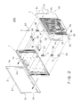
- FIG. 2 shows an exploded perspective view of the display panel 50A viewed from the rear side, illustrating how the display panel 50A is assembled which is described below.
- Two short brackets 5 (four short brackets in total) are attached to the liquid crystal display module 1 on both side edges and slid along the side edges by a specific distance. Then, the brackets 5 are engaged with side ribs (not shown in FIG. 2 and which will be described later) provided on the front cover 2 and fixed to the liquid crystal display module 1 with male screws S5.
- brackets 6 are attached to the liquid crystal display module 1 on the upper edge and slid along the upper edge by a specific distance. Then, the brackets 6 are engaged with upper ribs (not shown in FIG. 2 and which will be described later) provided on the front cover 2 and fixed to the liquid crystal display module 1 with male screws S6.
- a pair of angle brackets 7 are attached to the liquid crystal display module 1 on both side edges and slid along the side edges upwards by a specific distance. Then, the brackets 7 are engaged with side ribs and upper side ribs (not shown in FIG. 2 and which will be described later) provided on the front cover 2 and fixed to the liquid crystal display module 1 with male screws S7.
- the liquid crystal display module 1 is fit in the front cover 2 from the rear side of the front cover 2, with the short brackets 5, the long brackets 6, and the angle brackets 7 being engaged with several ribs after the brackets are slid in the orthogonal or lateral direction.
- the ribs are provided on both edges 2e and an upper edge 2f of a frame section 2c of the front cover 2, as protruding to the rear side of the front cover 2.
- the ribs can be formed by injection molding with a slide core mold.
- the liquid crystal display module 1 is then fixed to the front cover 2 with the male screws S5 to S7.
- the liquid crystal display module 1 is also fixed to the rear cover 3 with male screws S3 that are screwed into female screws (not shown) formed on the brackets 5 to 7, which will be described later in detail.
- the male screws S3, S5, S6 and S7 are not exposed to the front side of the front cover 2 but to the front side of the rear cover 3 (the rear side of the display panel 50A), thus maintaining a good appearance.
- FIG. 3 is a perspective view illustrating each of the four short brackets 5 shown in FIG. 2 .
- the short bracket 5 is made of a pressed sheet metal, having a rectangular-like base section 5a and a two-step bent section 5f connected to the base section 5a at one longitudinal side thereof.
- the two-step bent section 5f has a first bent section 5b and a second bent section 5c.
- the first bent section 5b is formed as being oblique to the base section 5a at about 45 degrees.
- the second bent section 5c is formed as being oblique to the base section 5a at about 90 degrees, or formed as having a reflex angle ⁇ of about (270 + ⁇ ) degrees ( ⁇ being a positive integer) to the base section 5a.
- the angle ⁇ is also an oblique angle of an inner surface 2e1, shown in FIG. 10 , of each edge 2e of the frame section 2c ( FIG. 2 ).
- the sign V in FIG. 10 indicates a line perpendicular to the screen 1a.
- the two-step bent section 5f has slits 5d formed on both ends in a way that each slit 5d straddles the first and second bent sections 5b and 5c. Each slit 5d is provided so that it can engage with a rib 2d provided to the front cover 2 ( FIG. 2 ), as shown in FIG. 12 , which will be described later in detail.
- a protruding section 5a1 Formed in the center of the base section 5a is a protruding section 5a1, that sticks out from the base section 5a in a direction opposite to the two-step bent section 5f, provided with a female screw 5a2. Formed along the protruding section 5a1 is a long oval hole 5e lying in the longitudinal direction of the base section 5a. Also formed on the base section 5a are a pair of through holes 5a3 on both sides of the protruding section 5a1.
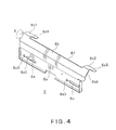
- FIG. 4 is a perspective view illustrating each of the two long brackets 6 shown in FIG. 2 .
- the long bracket 6 is made of a pressed sheet metal, having a rectangular-like base section 6a and a two-step bent section 6f connected to the base section 6a at one longitudinal side thereof.
- the two-step bent section 6f has a first bent section 6b and a pair of second bent sections 6c1 and 6c2 connected to the first bent section 6b at both ends thereof.
- the first bent section 6b is formed as being oblique to the base section 6a at about 45 degrees.
- the second bent sections 6c1 and 6c2 are formed as being oblique to the base section 6a at about 90 degrees, or formed as having a reflex angle ⁇ of about (270 + ⁇ ) degrees ( ⁇ being a positive integer) to the base section 6a.
- the angle ⁇ is also an oblique angle of the inner surface of the upper edge 2f of the frame section 2c ( FIG. 2 ).
- a slit 6d1 formed in a way that the slit 6d1 straddles the first bent section 6b and the second bent section 6c1.
- a tongue piece 6c3 that sticks out from an end 6bt of the first bent section 6b.
- the slit 6d1 and the tongue piece 6c3 are provided so that they can engage with ribs 2f5 and 2f6, respectively, both provided to the upper edge 2f of the frame section 2c of the front cover 2 ( FIG. 2 ), as shown in FIG. 13 , which will be described later in detail.
- the base section 6a is provided with a female screw 6a2, a pair of long oval holes 6e lying in the longitudinal direction of the base section 6a, and also a pair of through holes 6a3 adjacent to the long oval holes 6e in the longitudinal direction.
- FIG. 5 is a perspective view illustrating each of the two angle brackets 7 shown in FIG. 2 .
- the angle bracket 7 is made of a pressed sheet metal, having a rectangular-like base section 7a, a two-step bent section 7j connected to the base section 7a at one longitudinal side thereof, and a three-step bent section 7k connected to the base section 7a at one longitudinal end thereof.
- the two-step bent section 7j has a first bent section 7b and a second bent section 7c.
- the first bent section 7b is formed as being oblique to the base section 7a at about 45 degrees.
- the second bent section 7c is formed as being oblique to the base section 7a at about 90 degrees, or formed as having a reflex angle ⁇ of about (270 + ⁇ ) degrees ( ⁇ being a positive integer) to the base section 7a.
- the angle ⁇ is also an oblique angle of the inner surface of the upper edge 2f of the frame section 2c ( FIG. 2 ).
- a slit 7d formed in a way that the slit 7d straddles the bent sections 7b and 7c.
- the slit 7d is provided so that it can engage with a rib 2d2 provided to the side edge 2e of the frame section 2c of the front cover 2 ( FIG. 2 ), as shown in FIG. 14 , which will be described later in detail.
- the three-step bent section 7k has a first bent section 7f, a second bent section 7g, and a third bent section 7h.
- the first and second bent sections 7f and 7g are formed as being oblique to the base section 7a at about 45 and 90 degrees, respectively.
- the third bent section 7h is formed as being bent outwards so that it lies as parallel to the base section 7a.
- a slit 7i formed in a way that the slit 7i straddles the bent sections 7g and 7h.
- the slit 7i is provided so that it can engage with a rib 2f1 provided to the upper edge 2f of the frame section 2c of the front cover 2 ( FIG. 2 ), as shown in FIG. 15 , which will be described later in detail.
- a protruding section 7a1 Formed on the base section 7a is a protruding section 7a1, that sticks out from the base section 7a in a direction opposite to the two- and three-step bent sections 7j and 7k, provided with a female screw 7a2. Formed along the protruding section 7a1 is a long oval hole 7e lying in the longitudinal direction of the base section 7a. Also formed on the base section 7a is a through hole 7a3.
- liquid crystal display module 1 ( FIG. 1 ) with reference to FIGS. 6 to 14 .
- FIG. 6 is a perspective view illustrating the liquid crystal display module 1 viewed from the rear side thereof.
- the liquid crystal display module 1 is provided with: a base plate 1b made of a sheet metal; several cold cathode fluorescent lamps 1c (referred to as CCFL 1c, hereinafter, not shown in FIG. 6 but in FIGS. 1 and 9 ) arranged in parallel, each CCFL 1c lying in the longitudinal direction H; a pair of circuit boards 1d (inverter circuit boards in this embodiment) arranged on both sides of the module 1 in the rear side thereof, fixed to the base plate 1b with male screws (not shown); a pair of protecting covers 1e made of resin to cover the inverter circuit boards 1d; and also a light-diffusing panel assembly 11 and a liquid crystal display panel 12 (both shown in FIG. 10 ) arranged in front of the CCFLs 1c.
- CCFL 1c cold cathode fluorescent lamps 1c
- each circuit board 1d Mounted on each circuit board 1d are inverter circuits 1dk ( FIG. 9 ) that supply voltages to the CCFL 1c.
- the liquid crystal display module 1 is supported by a frame section 1j in which the base plate 1b is installed.
- the resin-made protecting covers 1e protect the inverter circuit boards 1d from damages and provide them with insulation. Moreover, the protecting covers 1e are provided so that a maintenance or service man can be protected from touching a high-voltage section, such as transformers 1d1, in the liquid crystal display module 1, and the module 1 can be protected from being damaged while shipped.
- each protecting cover 1e Provided on each protecting cover 1e are through holes 1e9 through which the transformers 1d1 are exposed, as described later.
- FIG. 9 a sectional view of the display panel 50A shown in (a) of FIG. 1 , taken on line S1 - S1 of FIG. 6 .
- each CCFL 1c is provided with electrodes 1c1 on both ends, which is supported by rubber spacers 1h fixed as being engaged with long oval holes 1b1 of the base plate 1b.
- Each electrode 1c1 is connected with flexible CCFL wirings 1g to a connector 1i mounted on the associated inverter circuit board 1d at one end.
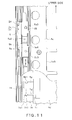
- FIG. 11 a plan view illustrating the fixing structure with each short bracket 5 ( FIG. 2 ).
- FIG. 11 shows the long oval hole 1b1 ( FIG. 9 ) provided on the base plate 1b as being opened in the longitudinal direction along each of the left and right sides of the frame section 2c ( FIG. 2 ).
- Each rubber spacer 1h can be seen through the long oval hole 1b1.
- the rubber spacer 1h is provided with a pair of wire supporters 1h1 formed as protruding from the spacer 1h.
- the wire supporters 1h1 go through the long oval hole 1b1 at both ends, as if each hole end is pinched by the associated supporter 1h1, and stick out from the base plate 1b to the rear side ( FIG. 1 ).
- the rubber spacer 1h are thus fixed to the base plate 1b with the wire supporters 1h1. Led out from the wire supporters 1h1 are the CCFL wirings 1g.
- the base plate 1b is provided with four base sections 1f at the upper edge, formed by stamping, as protruding from the base plate 1b in the rear side, as shown in FIG. 6 .
- FIG. 7 is a partial enlarged view illustrating each base section 1f.
- the dowel 1f1 is engaged with the associated long oval hole 6e of the long bracket 6 ( FIG. 4 ) so that the bracket 6 is slidable along the upper edge of the display panel 50A in FIG. 2 .
- the slide mechanism of the long bracket 6 allows the slit 6d1 and the tongue piece 6c3 (both shown in FIG. 4 ) to be engaged with the ribs 2f5 and 2f6, respectively, of the front cover 2 ( FIG. 13 ). After the engagement, each screw S6 ( FIG. 2 ) is inserted into the through hole 6a3 ( FIG. 4 ) and screwed into the female screw 1f2 ( FIG. 7 ) to fix the long bracket 6 to the base plate 1b ( FIG. 6 ), as shown in FIG. 2 .
- the number of the transformers 1d1 mounted on the inverter circuits 1d for supplying high voltages to the CCFLs 1c is equal to the number of the CCFLs 1c.
- Each transformer 1d1 is much higher than other components mounted on the associated inverter circuit 1d.
- the through holes 1e9 are provided on the protecting covers 1e for the transformers 1d1 to be exposed therethrough to give a small thickness TK to the reference rear section 3b of the housing 4 in (a) of FIG. 1 .
- FIG. 8 is a perspective view of the protecting cover 1e.
- FIG. 9 is a sectional view of the display panel 50A shown in (a) of FIG. 1 , taken on line S1 - S1 of FIG. 6 , as already mentioned.
- the protecting cover 1e is a rectangular-like flat cover provided with a stepped section 1e3 on a longitudinal edge section 1et side.
- the protecting cover 1e has: a higher section 1e1 that covers a zone AR1 in which the inverter circuit boards 1d are located; and a lower section 1e2 that covers a zone AR2, outside the zone AR1 in the longitudinal edge section 1et side, in which the wire supporters 1h1 are located.
- the lower section 1e2 is located closer to the base plate 1b than the higher section 1e1 is.
- dowels 1e4 also shown in FIG. 10 , are provided to the lower section 1e2 at a specific interval along the longitudinal edge section 1et.
- the stepped section 1e3 on the border of the zones AR1 and AR2 is located in a zone AR3, outside (in the left side in FIG. 9 ) an edge 1d2 of each inverter circuit board 1d, in which the CCFL wirings 1g are lying.
- the CCFL wirings 1g are flexible, they can be provided as being bent on the stepped section 1e3, thus achieving higher space utility.
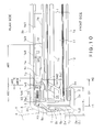
- Each CCFL wiring 1g may be provided so that its end at the associated inverter circuit board 1d side is positioned at the inner side than the edge 1d2 of the circuit board 1d, as shown in FIG. 10 (a modification).
- the stepped section 1e3 ( FIG. 8 ) is preferably located in a zone AR31 within the zone AR3 but terminated at the edge 1d2.
- the degree of step of the stepped section 1e3 in the thickness direction, or the front - to - rear (thickness) direction is referred to as a step degree D4, as shown in FIGS. 8 to 10 .
- each inverter circuit board 1d is provided as its edge 1d2 is positioned at a point H2 located inside the frame section 1j by a distance D1 from a point H1 that is the position of an inner side face 1j2 (shown only in FIG. 10 ) of the frame section 1j.
- the lower section 1e2 is located closer to the base plate 1b than the higher section 1e1 is.
- the lower section 1e2 covers the zone AR2 in which the wire supporters 1h1 are located.
- the higher section 1e1 covers the zone AR1 in which the inverter circuit boards 1e are located.
- the configuration described above provides spaces KS on both sides of the display panel 50A, each space KS corresponding to the step degree D4 of the stepped section 1e3 of the associated protecting cover 1e, on the rear side of the lower section 1e2 of the protecting cover 1e.
- the short brackets 5 are provided as the base sections 5a of the brackets 5 are installed in the spaces KS described above, which allows the thickness TK of the display panel 50A to be thinner with no effects of the thickness of each bracket 5 and other components associated with the bracket 5.
- FIG. 11 a plan view illustrating the fixing structure with the short bracket 5 ( FIG. 2 ), the short bracket 5 is configured as slidable in a direction Ds while the long oval hole 5e ( FIG. 3 ) is engaged with the associated dowel 1e4 ( FIG. 8 ) of the protecting cover 1e.
- the slide mechanism allows one of the slits 5d ( FIG. 3 ) of each short bracket 5 to be engaged with the rib 2d of the front cover 2 ( FIG. 2 ) so that the short bracket 5 is positioned at a certain location in the front - to - rear (thickness) direction.
- the rib 2d is formed as protruding inwardly from the side edge 2e in the frame section 2c of the front cover 2.
- each short bracket 5 When one of the slits 5d ( FIG. 3 ) of each short bracket 5 is engaged with the rib 2d of the front cover 2, as shown in FIGS. 11 and 12 , the screw S5 ( FIG. 2 ) is inserted into one of the through holes 5a3 and also one of several holes 1e5 provided on each protecting cover 1e, as shown in FIG. 8 , and then screwed into a female screw (not shown) of the base plate ( FIG. 6 ). Illustrated in FIG. 11 is that the screw S5 is inserted into the through hole 5a3 and the hole 1e5.
- the fixing structure described above offers a short distance D2 between the outer surface of the frame section 1j of the liquid crystal display module 1 and the inner surface 2e1 of the edge 2e of the frame section 2c of the frame cover 2, as shown in FIG. 9 .
- the distance D2 is very short almost equal to the thickness of each short bracket 5 with a narrow margin, thus achieving smaller widths WL and WR in (b) of FIG. 1 .
- Such a short distance D2 is also achieved by providing the second bent section 5c of each short bracket 5 so that the bent section 5c lies on the slant inner surface of the front cover 2 at the reflex angle ⁇ of about (270 + ⁇ ) degrees ( ⁇ being a positive integer) to the base section 5a.
- FIG. 13 a plan view illustrating the fixing structure with each long bracket 6 ( FIG. 2 ), the long bracket 6 is configured as slidable in a direction Ds2 while each long oval hole 6e ( FIG. 4 ) is engaged with the dowel 1f1 ( FIG. 7 ) of the associated base section 1f of the base plate 1b ( FIG. 6 ).
- the slide mechanism allows the slit 6d1 and the tongue piece 6c3 ( FIG. 4 ) of each long bracket 6 to be engaged with the ribs 2f5 and 2f6, respectively, of the front cover 2 ( FIG. 2 ) so that the long bracket 6 is positioned at a certain location in the front - to - rear (thickness) direction, or in the direction orthogonal to the plan view of FIG. 13 .
- the ribs 2f5 and 2f6 are formed as protruding inwardly from the upper edge 2f of the frame section 2c of the front cover 2.
- each long bracket 6 When the slit 6d1 and the tongue piece 6c3 of each long bracket 6 are engaged with the ribs 2f5 and 2f6, respectively, of the front cover 2, as shown in FIG. 13 , the screws S6 ( FIG. 2 ) are inserted into the through holes 6a3 and screwed into the female screws 1f2 ( FIG. 7 ) of the associated base section 1f of the base plate 1b ( FIG. 6 ), thus long bracket 6 being fixed on the base plate 1b.
- the fixing structure described above offers a short distance D3 between the outer surface of the frame section 1j of the liquid crystal display module 1 and the inner surface 2f2 of the upper edge 2f of the frame section 2c of the frame cover 2, as shown in FIG. 13 .
- the distance D3 is very short almost equal to the thickness of each long bracket 6 with a narrow margin, thus achieving a smaller width WT in (b) of FIG. 1 .
- FIG. 14 a plan view illustrating the fixing structure with each angle bracket 7 ( FIGS. 2 and 5 ), the angle bracket 7 is configured as slidable in a direction Ds along a long oval hole 7e while the hole 7e is engaged with one of the dowels 1e4 ( FIG. 8 ) of the associated protecting cover 1e.
- FIG. 15 is a fragmentary perspective view of the frame section 2c and the angle bracket 7 of FIG. 14 , viewed from lower right in FIG. 14 .
- the slide mechanism allows the slit 7i ( FIG. 5 ) of each angle bracket 7 to be engaged with a rib 2f1 of the front cover 2 ( FIG. 2 ) so that the angle bracket 7 is positioned at a certain location in the front - to - rear (thickness) direction.
- the rib 2f1 is formed as protruding inwardly from the upper edge 2f in the frame section 2c of the front cover 2.
- the rib 2f1 is constituted by a longitudinal rib 2f1a that lies in the thickness direction in which the slit 7c receives the rib 2f1a and a lateral rib 2f1b that touches an upper surface 7ht of the third bent section 7h of the three-step bent section 7k ( FIG. 5 ) to prevent the angle bracket 7 from being detached.
- the fixing structure described above offers a short distance D2 between the outer surface of the frame section 1j of the liquid crystal display module 1 and the inner surface 2e1 of the edge 2e of the frame section 2c of the frame cover 2, as shown in FIG. 9 .
- the distance D2 is very short almost equal to the thickness of each short bracket 5 with a narrow margin, thus achieving smaller widths WL and WR in (b) of FIG. 1 .
- the fixing structure described above offers a short distance D3 between an outer surface 1j2 of the frame section 1j of the liquid crystal display module 1 and an inner surface 2f2 of the frame section 2c of the frame cover 2, as shown in FIG. 13 .
- the distance D2 is very short almost equal to the thickness of each angle bracket 7 with the thickness of the ribs 2d2 and 2f1 and also a narrow margin, thus achieving narrower width WT in (b) of FIG. 1 .
- the through holes 3c are provided in counterbores 3z of the rear cover 3 which are provided as entering the space KS on both sides of the display panel 50A.
- a screw head S3t of each male screw S3 is allowed to remain in the associated counterbore 3z and thus prevented from protruding from the reference rear plane 3bf of the rear cover 3, shown in (a) of FIG. 1 , thus achieving a thinner liquid crystal display module 1.
- the liquid crystal display module 1 is fixed to the front cover 2 with the short, long, and angle brackets 5, 6, and 7 using the ribs 2d, 2d2, 2f1, 2f5, and 2f6 formed on the front cover 2 and to the rear cover 3 with the brackets 5, 6, and 7 with the screws S3.
- the ribs 2d, 2d2, 2f1, 2f5, and 2f6 are chamfered at their summits, as shown with a sign C in FIGS. 9 , 10 , 12 , and 15 , by which the liquid crystal display module 1 is smoothly and easily guided and fixed to the front cover 2.
- the height of each rib is adjusted as its summit almost touches the frame section 1j.
- the ribs 2d, 2d2, 2f1, 2f5, and 2f6 adjusted as described above allow the liquid crystal display module 1 to be fixed to the front cover 2 at an accurate position, particularly, with respect to the opening 2a through which the screen 1a is exposed, as shown in (b) of FIG. 1 , thus appropriate for mass production.
- the ribs 2d, 2d2, 2f1, 2f5, and 2f6 are adjusted as their summits almost touch the frame section 1j, the ribs immediately touch and prevent the frame section 1j from being deformed when the front cover 2 is pressed by fingers for example, thus providing a highly rigid housing 4.
- the short, long and angle brackets 5, 6 and 7 are provided with the first bent sections 5b, 6b and 7f, respectively.
- the bent sections 5b, 6b and 7f are formed as oblique to the base sections 5a, 6a and 7a, respectively, at about 45 degrees, as shown in FIGS. 3 , 4 and 5 , respectively.
- the configuration to the brackets 5, 6 and 7 allows a side face 3m ( FIG. 9 ) of the rear cover 3 to be formed as being tapered to the rear side which makes the display panel 50A ( FIG. 1 ) look like a slim panel, thus effective in panel design.
- the inverter circuits 1d are installed in the liquid crystal display module 1 so that the edge of each circuit 1d is positioned inside the left and right side faces of the module 1. This installation gives the space KS ( FIG. 9 ) on both sides of the circuit 1d, that corresponds to the thickness of each circuit 1d.
- the space KS creates a rectangular shape in the liquid crystal display module 1, constituted by the length Lc of each protecting cover 1e in the longitudinal direction, the step degree D4 of the stepped section 1e3, and zone AR2 of the lower section 1e2, shown in FIG. 8 .
- each space KS is a fixing means for fixing the liquid crystal display module 1 to the housing 4, which makes the housing 4 thinner at the location in which the fixing means is provided than at the location in which each inverter circuit 1d is installed, thus achieving a thinner housing 4.
- the fixing means installed in the spaces KS described above are the short and angle brackets 5 and 7, in this embodiment, with the sheet-metal bent sections having the slits 5d and 7d, respectively, engaged with the ribs 2d, and 2d2 and 2f1, respectively, formed as protruding from the housing to inside, to fix the liquid crystal display module 1 in the housing 4.
- the fixing structure allows the gap between the module 1 in the housing 4 to be narrow as almost corresponding to the thickness of the the short and angle brackets 5 and 7.
- the display apparatus 50 having the configuration with the fixing structure described above can have a narrow edge section 2c concerning the widths WL, WR, and WT, as shown in (b) of FIG. 1 .
- the angle brackets 7 are not essential components for a display apparatus with a relatively small display panel. Nevertheless, the angle brackets 7 are very effective components for a display apparatus with a large (for example, 42 inches or larger) display panel, to effectively prevent the front cover 2 from being deformed.
- the display apparatus 50 described above requires the mount 50B to support the display panel 50A.
- the present invention is applicable to a display apparatus with no such mount, such as a hung-on-wall type.
- the display apparatus 50 described above is a 46-inch television
- the present invention is applicable to any screen size.
- the display module 1 described above is a liquid crystal display module
- the present invention is applicable to any types of display module, such as an organic electro-luminescence type.
- the present invention can employ other tube-type light sources, such as EEFL, with inverter circuit boards are smaller or larger than those for CCFL.
- circuit boards 1d described above are the inverter circuit boards, any types of circuit boards are available in the present invention.
- the front cover is provided for protecting the circuit boards from damages in shipping, maintenance, etc., but still, the space KS described above is created.
- the fixing means for fixing the display module 1 to the housing 4 allows the housing 4 to be made thinner at the location in which the fixing means is provided than at the location in which each inverter circuit 1d is installed, thus achieving a thinner housing 4.
- the fixing structure described above can be provided at the upper and lower edges of the housing 4 when the circuit boards 1d are provided at the upper and lower edges of the display module 1.
- the present invention achieves a thinner display panel held by a frame having a narrower edge that surrounds the display panel.
Landscapes
- Physics & Mathematics (AREA)
- Nonlinear Science (AREA)
- Mathematical Physics (AREA)
- Chemical & Material Sciences (AREA)
- Crystallography & Structural Chemistry (AREA)
- General Physics & Mathematics (AREA)
- Optics & Photonics (AREA)
- Liquid Crystal (AREA)
- Devices For Indicating Variable Information By Combining Individual Elements (AREA)
Abstract
Description
- This application is based on and claims the benefit of priority from the prior Japanese Patent Application Nos.
2008 - 059438 filed on March 10, 2008 2008 - 300621 filed on November 26, 2008 - The present invention relates to a display module, a fixing structure for the display module and a display apparatus, for a thin display panel held by a frame having a narrow edge that surrounds the display panel.
- In recent years, display apparatuses or television apparatuses to display images through a liquid crystal display module have rapidly become popular.
- Such display apparatuses usually consist of: a display panel having a frame for holding a display module, a display screen thereof being installed in the frame for viewing; and a mount to support the display panel so that the display panel can be turned in the perpendicular and lateral directions.
- Liquid crystal display modules require a backlight device with light sources, such as, cold cathode fluorescent lamps (CCFL) and external electrode fluorescent lamps (EEFL).
- In such image display apparatuses, a display module is held by a frame with screws turned into bosses formed on the frame (such as disclosed in Japanese Un-examined Patent Publication No.
2000 - 305068 2003 - 140117 Citations - With higher popularity of image display apparatuses, there are higher demands for a thinner display panel and a frame for holding the screen of the display panel with a narrower frame edge that surrounds the screen, particularly on the upper edge section and the side edge sections, except for the bottom edge section closer to the mount for supporting the display panel.
- The assembly of a display panel in which a display module is held by a frame with screws, such as disclosed in
Citation 1, however, requires the space for bosses on the outer edge of the frame, thus restricting, at least, on the width of the edge that surrounds the screen, in achieving a narrower frame edge. - The assembly of a display panel in which a display module is held on a frame with fixing members of the module engaged with ribs of the frame, such as disclosed in
Citation 2, is relatively effective in achieving a narrower frame edge. Such fixing members are, however, provided on the display module as protruding in the thickness direction, and hence not appropriate for achieving a thinner display panel. Particularly, a liquid crystal display panel requires power supply circuits, such as inverters, for supplying power to light sources, provided on the side edges of a display module on both sides of a screen, and hence posing a big problem in achieving a thinner display panel. - Such problems discussed above are explained more in detail with respect to
FIG. 16 . -
FIG. 16 shows a schematic perspective rear view of a known liquidcrystal display module 101, showing the rear side of the module viewed from above. - Installed in the liquid
crystal display module 101 are several cold cathode fluorescent lamps (CCFL) 102, as backlights, arranged in parallel in the longitudinal direction H, on the front side of abase 104 of themodule 101, in order to illuminating a screen (not shown) on the front side. - Also installed in the liquid
crystal display module 101 areinverter circuits 103 provided on both rear edge sides of thebase 104, that supply voltages toelectrodes 102a of eachCCFL 102 through CCFL wirings (not shown). Usually, the CCFL wirings are made as short as possible for stably driving the CCFL 102. - The
inverter circuits 103 provided on both sides of the liquidcrystal display module 101 pose difficulty in achieving a thinner display panel difficult. - A purpose of the present invention is to provide a display module, a fixing structure for the display module and a display apparatus, achieving a thinner display panel held by a frame having a narrower edge that surrounds the display panel, with circuit boards on both sides of the display module.
- The present invention provides a display module comprising: a base plate having a front surface section and a rear surface section that has at least one edge section; a display panel provided on the front surface section of the base plate; a circuit board provided in a specific zone of the rear surface section of the base plate in which the specific zone is closer to the edge section of the rear surface section of the base plate than a center of the rear surface section is; and a protecting cover to protect the circuit board and the base plate wherein the protecting cover has a higher section and a lower section that is closer to the base plate than the higher section is so that the higher section at least partially covers the circuit board while the lower section at least partially covers the base plate, the higher and lower sections giving a space inside the display module but outside the protecting cover, the space having a height corresponding to a step crated by the higher and lower sections and being located between the specific zone and the edge section of the rear surface section of the base plate.
- Moreover, the present invention provides a fixing structure for fixing a display module, comprising: a cover; and a fixing component to fix the display module to the cover, wherein the display module includes: a base plate having a front surface section and a rear surface section that has at least one edge section; a display panel provided on the front surface section of the base plate; a circuit board provided in a specific zone of the rear surface section of the base plate in which the specific zone is closer to the edge section of the rear surface section of the base plate than a center of the rear surface section is; and a protecting cover to protect the circuit board and the base plate wherein the protecting cover has a higher section and a lower section that is closer to the base plate than the higher section is so that the higher section at least partially covers the circuit board while the lower section at least partially covers the base plate, the higher and lower sections giving a space inside the display module but outside the protecting cover, the space having a height corresponding to a step created by the higher and lower sections and being located between the specific zone and the edge section of the rear surface section of the base plate, wherein the fixing component is at least partially installed in the space and attached to the base plate.
- Furthermore, the present invention provides a display apparatus comprising: a cover; a display module; and a fixing component to fix the display module to the cover, wherein the display module includes: a base plate having a front surface section and a rear surface section that has at least one edge section; a display panel provided on the front surface section of the base plate; a circuit board provided in a specific zone of the rear surface section of the base plate in which the specific zone is closer to the edge section of the rear surface section of the base plate than a center of the rear surface section is; and a protecting cover to protect the circuit board and the base plate wherein the protecting cover has a higher section and a lower section that is closer to the base plate than the higher section is so that the higher section at least partially covers the circuit board while the lower section at least partially covers the base plate, the higher and lower sections giving a space inside the display module but outside the protecting cover, the space having a height corresponding to a step created by the higher and lower sections and being located between the specific zone and the edge section of the rear surface section of the base plate, wherein the fixing component is at least partially installed in the space and attached to the base plate.
-
-
FIG. 1 shows external perspective views of a display apparatus according to the present invention, in which (a) and (b) show the rear and front sides, respectively, of the display apparatus viewed from above; -
FIG. 2 shows a fragmentary perspective view of a display apparatus according to the present invention; -
FIG. 3 is a perspective view illustrating a short bracket to be used as a first component of a fixing structure for a display apparatus according to the present invention; -
FIG. 4 is a perspective view illustrating a long bracket used as a second component of the fixing structure for a display apparatus according to the present invention; -
FIG. 5 is a perspective view illustrating an angle bracket used as a third component of the fixing structure for a display apparatus according to the present invention; -
FIG. 6 is a perspective view illustrating a display module installed in a display apparatus according to the present invention; -
FIG. 7 is a partial enlarged view illustrating a base section of the display module shown inFIG. 6 , according to the present invention; -
FIG. 8 is a perspective view of a protecting cover used for a liquid crystal display module installed in a display apparatus according to the present invention; -
FIG. 9 is a partial sectional view illustrating a display panel shown in (a) ofFIG. 1 , taken on line S1 - S1 ofFIG. 6 ; -
FIG. 10 is a partial sectional view illustrating a modification to a display module installed in a display apparatus according to the present invention, taken on line S1 -S1 ofFIG. 6 ; -
FIG. 11 is a plan view illustrating a fixing structure for a display apparatus according to the present invention; -
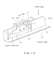
FIG. 12 is a perspective view illustrating the fixing structure for a display apparatus according to the present invention; -
FIG. 13 is a plan view illustrating the fixing structure for a display apparatus according to the present invention; -
FIG. 14 is a plan view illustrating the fixing structure for a display apparatus according to the present invention; -
FIG. 15 is a perspective view illustrating the fixing structure for a display apparatus according to the present invention; and -
FIG. 16 is a perspective view illustrating a known display module. - In the following disclosure and throughout the drawings, the same or analogous elements or components are given the same numerals or signs, the overlapping description being omitted if not necessary.
-
FIG. 1 shows external perspective views of adisplay apparatus 50 according to the present invention, in which (a) and (b) show the rear and front sides, respectively, of the display apparatus viewed from above. - The
display apparatus 50 shown inFIG. 1 is a 46-inch television equipped with a liquidcrystal display module 1, in this embodiment, that consists of: adisplay panel 50A having thedisplay module 1 installed therein; and amount 50B to support thedisplay panel 50A so that thedisplay panel 50A can be turned in the perpendicular and lateral directions. - The
display panel 50A has a housing 4 with afront cover 2 that is a frame and arear cover 3 that is a flat box with an opening on one side. Installed in the housing 4 is the liquidcrystal display module 1 held by a fixing structure which will be described later. - Formed on the
rear cover 3 is a protruding cover section 3a that protrudes in the rear side, as shown in (a) ofFIG. 1 . Installed in the cover section 3a are a circuit board for television signal processing, a power supply, etc. (not shown). - In the
rear cover 3, the zone except for the protruding cover section 3a is referred to as a referencerear section 3b, hereinafter. The plane of the referencerear section 3b is referred to as a reference rear plane 3bf, hereinafter. - The
front cover 2 has anopening 2a for ascreen 1a of the liquidcrystal display module 1 to be installed, as shown in (b) ofFIG. 1 . The frame section that surrounds theopening 2a is referred to as anedge section 2c. The front-side plane of thefront cover 2 is referred to as areference front plane 2b, hereinafter. - In (a) and (b) of
FIG. 1 , the dimensions of the housing 4 are defined as follows: - TK: a thickness of the reference
rear section 3b, the zone except for the protruding cover section 3a, corresponding to the distance between thereference front plane 2b and the reference rear plane 3bf; - WT: a width between the upper edge of the
front cover 2 and the opening 2a; - WL: a width between the left-side edge of the
front cover 2 and the opening 2a; and - WR: a width between the right-side edge of the
front cover 2 and the opening 2a. - According to the definition, a smaller thickness TK provides a
thinner display panel 50A and shorter distances WT, WL and WR provide anarrower edge section 2c. -
FIG. 2 shows an exploded perspective view of thedisplay panel 50A viewed from the rear side, illustrating how thedisplay panel 50A is assembled which is described below. - Two short brackets 5 (four short brackets in total) are attached to the liquid
crystal display module 1 on both side edges and slid along the side edges by a specific distance. Then, thebrackets 5 are engaged with side ribs (not shown inFIG. 2 and which will be described later) provided on thefront cover 2 and fixed to the liquidcrystal display module 1 with male screws S5. - Likewise, two
long brackets 6 are attached to the liquidcrystal display module 1 on the upper edge and slid along the upper edge by a specific distance. Then, thebrackets 6 are engaged with upper ribs (not shown inFIG. 2 and which will be described later) provided on thefront cover 2 and fixed to the liquidcrystal display module 1 with male screws S6. - Moreover, a pair of
angle brackets 7 are attached to the liquidcrystal display module 1 on both side edges and slid along the side edges upwards by a specific distance. Then, thebrackets 7 are engaged with side ribs and upper side ribs (not shown inFIG. 2 and which will be described later) provided on thefront cover 2 and fixed to the liquidcrystal display module 1 with male screws S7. - With the assembly procedure described above, the liquid
crystal display module 1 is fit in thefront cover 2 from the rear side of thefront cover 2, with theshort brackets 5, thelong brackets 6, and theangle brackets 7 being engaged with several ribs after the brackets are slid in the orthogonal or lateral direction. - Although not shown in
FIG. 2 , the ribs are provided on bothedges 2e and anupper edge 2f of aframe section 2c of thefront cover 2, as protruding to the rear side of thefront cover 2. The ribs can be formed by injection molding with a slide core mold. - The slide mechanism provided for each of the
brackets 5 to 7 will be described later in detail. - The liquid
crystal display module 1 is then fixed to thefront cover 2 with the male screws S5 to S7. - The liquid
crystal display module 1 is also fixed to therear cover 3 with male screws S3 that are screwed into female screws (not shown) formed on thebrackets 5 to 7, which will be described later in detail. - In this procedure, all of the male screws S3, S5, S6 and S7 are screwed from the rear to the front side, as shown in
FIG. 2 , thus achieving an efficient assembly procedure. - Moreover, the male screws S3, S5, S6 and S7 are not exposed to the front side of the
front cover 2 but to the front side of the rear cover 3 (the rear side of thedisplay panel 50A), thus maintaining a good appearance. -
FIG. 3 is a perspective view illustrating each of the fourshort brackets 5 shown inFIG. 2 . - The
short bracket 5 is made of a pressed sheet metal, having a rectangular-like base section 5a and a two-stepbent section 5f connected to thebase section 5a at one longitudinal side thereof. - The two-step
bent section 5f has a firstbent section 5b and a secondbent section 5c. The firstbent section 5b is formed as being oblique to thebase section 5a at about 45 degrees. The secondbent section 5c is formed as being oblique to thebase section 5a at about 90 degrees, or formed as having a reflex angle Θ of about (270 + α) degrees (α being a positive integer) to thebase section 5a. - The angle α is also an oblique angle of an inner surface 2e1, shown in
FIG. 10 , of eachedge 2e of theframe section 2c (FIG. 2 ). The sign V inFIG. 10 indicates a line perpendicular to thescreen 1a. - The two-step
bent section 5f hasslits 5d formed on both ends in a way that eachslit 5d straddles the first and secondbent sections slit 5d is provided so that it can engage with arib 2d provided to the front cover 2 (FIG. 2 ), as shown inFIG. 12 , which will be described later in detail. - Formed in the center of the
base section 5a is a protruding section 5a1, that sticks out from thebase section 5a in a direction opposite to the two-stepbent section 5f, provided with a female screw 5a2. Formed along the protruding section 5a1 is a longoval hole 5e lying in the longitudinal direction of thebase section 5a. Also formed on thebase section 5a are a pair of through holes 5a3 on both sides of the protruding section 5a1. -
FIG. 4 is a perspective view illustrating each of the twolong brackets 6 shown inFIG. 2 . - The
long bracket 6 is made of a pressed sheet metal, having a rectangular-like base section 6a and a two-stepbent section 6f connected to the base section 6a at one longitudinal side thereof. - The two-step
bent section 6f has a firstbent section 6b and a pair of second bent sections 6c1 and 6c2 connected to the firstbent section 6b at both ends thereof. The firstbent section 6b is formed as being oblique to the base section 6a at about 45 degrees. The second bent sections 6c1 and 6c2 are formed as being oblique to the base section 6a at about 90 degrees, or formed as having a reflex angle Θ of about (270 + β) degrees (β being a positive integer) to the base section 6a. The angle β is also an oblique angle of the inner surface of theupper edge 2f of theframe section 2c (FIG. 2 ). - Provided to the first
bent section 6b and the second bent section 6c1 is a slit 6d1 formed in a way that the slit 6d1 straddles the firstbent section 6b and the second bent section 6c1. Provided to the second bent section 6c2 is a tongue piece 6c3 that sticks out from an end 6bt of the firstbent section 6b. The slit 6d1 and the tongue piece 6c3 are provided so that they can engage with ribs 2f5 and 2f6, respectively, both provided to theupper edge 2f of theframe section 2c of the front cover 2 (FIG. 2 ), as shown inFIG. 13 , which will be described later in detail. - The base section 6a is provided with a female screw 6a2, a pair of
long oval holes 6e lying in the longitudinal direction of the base section 6a, and also a pair of through holes 6a3 adjacent to thelong oval holes 6e in the longitudinal direction. -
FIG. 5 is a perspective view illustrating each of the twoangle brackets 7 shown inFIG. 2 . - The
angle bracket 7 is made of a pressed sheet metal, having a rectangular-like base section 7a, a two-step bent section 7j connected to the base section 7a at one longitudinal side thereof, and a three-stepbent section 7k connected to the base section 7a at one longitudinal end thereof. - The two-step bent section 7j has a first
bent section 7b and a secondbent section 7c. The firstbent section 7b is formed as being oblique to the base section 7a at about 45 degrees. The secondbent section 7c is formed as being oblique to the base section 7a at about 90 degrees, or formed as having a reflex angle Θ of about (270 + β) degrees (β being a positive integer) to the base section 7a. The angle β is also an oblique angle of the inner surface of theupper edge 2f of theframe section 2c (FIG. 2 ). - Provided to the first and second
bent sections slit 7d formed in a way that theslit 7d straddles thebent sections slit 7d is provided so that it can engage with a rib 2d2 provided to theside edge 2e of theframe section 2c of the front cover 2 (FIG. 2 ), as shown inFIG. 14 , which will be described later in detail. - The three-step
bent section 7k has a firstbent section 7f, a second bent section 7g, and a thirdbent section 7h. The first and secondbent sections 7f and 7g are formed as being oblique to the base section 7a at about 45 and 90 degrees, respectively. The thirdbent section 7h is formed as being bent outwards so that it lies as parallel to the base section 7a. - Provided to the second and third
bent sections 7g and 7h is aslit 7i formed in a way that theslit 7i straddles thebent sections 7g and 7h. Theslit 7i is provided so that it can engage with a rib 2f1 provided to theupper edge 2f of theframe section 2c of the front cover 2 (FIG. 2 ), as shown inFIG. 15 , which will be described later in detail. - Formed on the base section 7a is a protruding section 7a1, that sticks out from the base section 7a in a direction opposite to the two- and three-step
bent sections 7j and 7k, provided with a female screw 7a2. Formed along the protruding section 7a1 is a longoval hole 7e lying in the longitudinal direction of the base section 7a. Also formed on the base section 7a is a through hole 7a3. - Described next is the liquid crystal display module 1 (
FIG. 1 ) with reference toFIGS. 6 to 14 . -
FIG. 6 is a perspective view illustrating the liquidcrystal display module 1 viewed from the rear side thereof. - In
FIG. 6 , the liquidcrystal display module 1 is provided with: abase plate 1b made of a sheet metal; several coldcathode fluorescent lamps 1c (referred to asCCFL 1c, hereinafter, not shown inFIG. 6 but inFIGS. 1 and9 ) arranged in parallel, eachCCFL 1c lying in the longitudinal direction H; a pair ofcircuit boards 1d (inverter circuit boards in this embodiment) arranged on both sides of themodule 1 in the rear side thereof, fixed to thebase plate 1b with male screws (not shown); a pair of protectingcovers 1e made of resin to cover theinverter circuit boards 1d; and also a light-diffusingpanel assembly 11 and a liquid crystal display panel 12 (both shown inFIG. 10 ) arranged in front of theCCFLs 1c. - Mounted on each
circuit board 1d are inverter circuits 1dk (FIG. 9 ) that supply voltages to theCCFL 1c. - The liquid
crystal display module 1 is supported by aframe section 1j in which thebase plate 1b is installed. - The resin-made
protecting covers 1e protect theinverter circuit boards 1d from damages and provide them with insulation. Moreover, the protectingcovers 1e are provided so that a maintenance or service man can be protected from touching a high-voltage section, such as transformers 1d1, in the liquidcrystal display module 1, and themodule 1 can be protected from being damaged while shipped. - Provided on each protecting
cover 1e are through holes 1e9 through which the transformers 1d1 are exposed, as described later. - The wiring between the
inverter circuit boards 1d and theCCFLs 1c is described with reference toFIG. 9 , a sectional view of thedisplay panel 50A shown in (a) ofFIG. 1 , taken on line S1 - S1 ofFIG. 6 . - In
FIG. 9 , eachCCFL 1c is provided with electrodes 1c1 on both ends, which is supported byrubber spacers 1h fixed as being engaged with long oval holes 1b1 of thebase plate 1b. Each electrode 1c1 is connected withflexible CCFL wirings 1g to aconnector 1i mounted on the associatedinverter circuit board 1d at one end. - The wiring is also shown in
FIG. 11 , a plan view illustrating the fixing structure with each short bracket 5 (FIG. 2 ). -
FIG. 11 shows the long oval hole 1b1 (FIG. 9 ) provided on thebase plate 1b as being opened in the longitudinal direction along each of the left and right sides of theframe section 2c (FIG. 2 ). - Each
rubber spacer 1h can be seen through the long oval hole 1b1. Therubber spacer 1h is provided with a pair of wire supporters 1h1 formed as protruding from thespacer 1h. The wire supporters 1h1 go through the long oval hole 1b1 at both ends, as if each hole end is pinched by the associated supporter 1h1, and stick out from thebase plate 1b to the rear side (FIG. 1 ). Therubber spacer 1h are thus fixed to thebase plate 1b with the wire supporters 1h1. Led out from the wire supporters 1h1 are theCCFL wirings 1g. - The
base plate 1b is provided with four base sections 1f at the upper edge, formed by stamping, as protruding from thebase plate 1b in the rear side, as shown inFIG. 6 . -
FIG. 7 is a partial enlarged view illustrating each base section 1f. Provided on the base section 1f are a dowel 1f1 and a female screw 1f2. The dowel 1f1 is engaged with the associated longoval hole 6e of the long bracket 6 (FIG. 4 ) so that thebracket 6 is slidable along the upper edge of thedisplay panel 50A inFIG. 2 . - The slide mechanism of the
long bracket 6 allows the slit 6d1 and the tongue piece 6c3 (both shown inFIG. 4 ) to be engaged with the ribs 2f5 and 2f6, respectively, of the front cover 2 (FIG. 13 ). After the engagement, each screw S6 (FIG. 2 ) is inserted into the through hole 6a3 (FIG. 4 ) and screwed into the female screw 1f2 (FIG. 7 ) to fix thelong bracket 6 to thebase plate 1b (FIG. 6 ), as shown inFIG. 2 . - In
FIG. 6 , the number of the transformers 1d1 mounted on theinverter circuits 1d for supplying high voltages to theCCFLs 1c is equal to the number of theCCFLs 1c. Each transformer 1d1 is much higher than other components mounted on the associatedinverter circuit 1d. Thus, the through holes 1e9 are provided on the protecting covers 1e for the transformers 1d1 to be exposed therethrough to give a small thickness TK to the referencerear section 3b of the housing 4 in (a) ofFIG. 1 . - Described next with reference to
FIGS. 8 and9 is each resin-made protectingcover 1e shown inFIG. 6 .FIG. 8 is a perspective view of the protectingcover 1e.FIG. 9 is a sectional view of thedisplay panel 50A shown in (a) ofFIG. 1 , taken on line S1 - S1 ofFIG. 6 , as already mentioned. - As shown in
FIG. 8 , the protectingcover 1e is a rectangular-like flat cover provided with a stepped section 1e3 on a longitudinal edge section 1et side. - In
FIGS. 8 and9 , the protectingcover 1e has: a higher section 1e1 that covers a zone AR1 in which theinverter circuit boards 1d are located; and a lower section 1e2 that covers a zone AR2, outside the zone AR1 in the longitudinal edge section 1et side, in which the wire supporters 1h1 are located. The lower section 1e2 is located closer to thebase plate 1b than the higher section 1e1 is. Several dowels 1e4, also shown inFIG. 10 , are provided to the lower section 1e2 at a specific interval along the longitudinal edge section 1et. - The stepped section 1e3 on the border of the zones AR1 and AR2 is located in a zone AR3, outside (in the left side in
FIG. 9 ) an edge 1d2 of eachinverter circuit board 1d, in which theCCFL wirings 1g are lying. - Since the
CCFL wirings 1g are flexible, they can be provided as being bent on the stepped section 1e3, thus achieving higher space utility. - Each
CCFL wiring 1g may be provided so that its end at the associatedinverter circuit board 1d side is positioned at the inner side than the edge 1d2 of thecircuit board 1d, as shown inFIG. 10 (a modification). In such an arrangement, the stepped section 1e3 (FIG. 8 ) is preferably located in a zone AR31 within the zone AR3 but terminated at the edge 1d2. - The degree of step of the stepped section 1e3 in the thickness direction, or the front - to - rear (thickness) direction is referred to as a step degree D4, as shown in
FIGS. 8 to 10 . - In
FIGS. 9 and10 , eachinverter circuit board 1d is provided as its edge 1d2 is positioned at a point H2 located inside theframe section 1j by a distance D1 from a point H1 that is the position of an inner side face 1j2 (shown only inFIG. 10 ) of theframe section 1j. - In each protecting
cover 1e, as already described, the lower section 1e2 is located closer to thebase plate 1b than the higher section 1e1 is. Here, the lower section 1e2 covers the zone AR2 in which the wire supporters 1h1 are located. The higher section 1e1 covers the zone AR1 in which theinverter circuit boards 1e are located. - The configuration described above provides spaces KS on both sides of the
display panel 50A, each space KS corresponding to the step degree D4 of the stepped section 1e3 of the associated protectingcover 1e, on the rear side of the lower section 1e2 of the protectingcover 1e. - Then, the
short brackets 5 are provided as thebase sections 5a of thebrackets 5 are installed in the spaces KS described above, which allows the thickness TK of thedisplay panel 50A to be thinner with no effects of the thickness of eachbracket 5 and other components associated with thebracket 5. - In
FIG. 11 , a plan view illustrating the fixing structure with the short bracket 5 (FIG. 2 ), theshort bracket 5 is configured as slidable in a direction Ds while the longoval hole 5e (FIG. 3 ) is engaged with the associated dowel 1e4 (FIG. 8 ) of the protectingcover 1e. - Then, as shown in
FIG. 12 , the slide mechanism allows one of theslits 5d (FIG. 3 ) of eachshort bracket 5 to be engaged with therib 2d of the front cover 2 (FIG. 2 ) so that theshort bracket 5 is positioned at a certain location in the front - to - rear (thickness) direction. InFIG. 12 , therib 2d is formed as protruding inwardly from theside edge 2e in theframe section 2c of thefront cover 2. - When one of the
slits 5d (FIG. 3 ) of eachshort bracket 5 is engaged with therib 2d of thefront cover 2, as shown inFIGS. 11 and12 , the screw S5 (FIG. 2 ) is inserted into one of the through holes 5a3 and also one of several holes 1e5 provided on each protectingcover 1e, as shown inFIG. 8 , and then screwed into a female screw (not shown) of the base plate (FIG. 6 ). Illustrated inFIG. 11 is that the screw S5 is inserted into the through hole 5a3 and the hole 1e5. - The fixing structure described above offers a short distance D2 between the outer surface of the
frame section 1j of the liquidcrystal display module 1 and the inner surface 2e1 of theedge 2e of theframe section 2c of theframe cover 2, as shown inFIG. 9 . The distance D2 is very short almost equal to the thickness of eachshort bracket 5 with a narrow margin, thus achieving smaller widths WL and WR in (b) ofFIG. 1 . - Such a short distance D2 is also achieved by providing the second
bent section 5c of eachshort bracket 5 so that thebent section 5c lies on the slant inner surface of thefront cover 2 at the reflex angle Θ of about (270 + α) degrees (α being a positive integer) to thebase section 5a. - In
FIG. 13 , a plan view illustrating the fixing structure with each long bracket 6 (FIG. 2 ), thelong bracket 6 is configured as slidable in a direction Ds2 while eachlong oval hole 6e (FIG. 4 ) is engaged with the dowel 1f1 (FIG. 7 ) of the associated base section 1f of thebase plate 1b (FIG. 6 ). - Then, as shown in
FIG. 13 , the slide mechanism allows the slit 6d1 and the tongue piece 6c3 (FIG. 4 ) of eachlong bracket 6 to be engaged with the ribs 2f5 and 2f6, respectively, of the front cover 2 (FIG. 2 ) so that thelong bracket 6 is positioned at a certain location in the front - to - rear (thickness) direction, or in the direction orthogonal to the plan view ofFIG. 13 . InFIG. 13 , the ribs 2f5 and 2f6 are formed as protruding inwardly from theupper edge 2f of theframe section 2c of thefront cover 2. - When the slit 6d1 and the tongue piece 6c3 of each
long bracket 6 are engaged with the ribs 2f5 and 2f6, respectively, of thefront cover 2, as shown inFIG. 13 , the screws S6 (FIG. 2 ) are inserted into the through holes 6a3 and screwed into the female screws 1f2 (FIG. 7 ) of the associated base section 1f of thebase plate 1b (FIG. 6 ), thuslong bracket 6 being fixed on thebase plate 1b. - The fixing structure described above offers a short distance D3 between the outer surface of the
frame section 1j of the liquidcrystal display module 1 and the inner surface 2f2 of theupper edge 2f of theframe section 2c of theframe cover 2, as shown inFIG. 13 . The distance D3 is very short almost equal to the thickness of eachlong bracket 6 with a narrow margin, thus achieving a smaller width WT in (b) ofFIG. 1 . - In
FIG. 14 , a plan view illustrating the fixing structure with each angle bracket 7 (FIGS. 2 and5 ), theangle bracket 7 is configured as slidable in a direction Ds along a longoval hole 7e while thehole 7e is engaged with one of the dowels 1e4 (FIG. 8 ) of the associated protectingcover 1e. - Then, as shown in
FIG. 15 , the slide mechanism allows theslit 7d (FIG. 5 ) of eachangle bracket 7 to be engaged with a rib 2d2 of the front cover 2 (FIG. 2 ) so that theangle bracket 7 is positioned at a certain location in the front - to - rear (thickness) direction. InFIG. 14 , the rib 2d2 is formed as protruding inwardly from theside edge 2e in theframe section 2c of thefront cover 2.FIG. 15 is a fragmentary perspective view of theframe section 2c and theangle bracket 7 ofFIG. 14 , viewed from lower right inFIG. 14 . - Moreover, in
FIG. 15 , the slide mechanism allows theslit 7i (FIG. 5 ) of eachangle bracket 7 to be engaged with a rib 2f1 of the front cover 2 (FIG. 2 ) so that theangle bracket 7 is positioned at a certain location in the front - to - rear (thickness) direction. InFIG. 15 , the rib 2f1 is formed as protruding inwardly from theupper edge 2f in theframe section 2c of thefront cover 2. The rib 2f1 is constituted by a longitudinal rib 2f1a that lies in the thickness direction in which theslit 7c receives the rib 2f1a and a lateral rib 2f1b that touches an upper surface 7ht of the thirdbent section 7h of the three-stepbent section 7k (FIG. 5 ) to prevent theangle bracket 7 from being detached. - The engagement of the
slits ribs 2d and 2f1, respectively, prevents thefront panel 2 from being deformed which otherwise tends to occur at the corners of thepanel 2 for a larger screen. - As already described, when one of the
slits 5d of each short bracket 5 (FIG. 3 ) is engaged with therib 2d of thefront cover 2, as shown inFIGS. 11 and12 , the screw S5 (FIG. 2 ) is inserted into one of the through holes 5a3 and also one of the holes 1e5 provided on each protectingcover 1e, as shown inFIG. 8 , and then screwed into a female screw (not shown) of thebase plate 1b (FIG. 6 ). - The fixing structure described above offers a short distance D2 between the outer surface of the
frame section 1j of the liquidcrystal display module 1 and the inner surface 2e1 of theedge 2e of theframe section 2c of theframe cover 2, as shown inFIG. 9 . The distance D2 is very short almost equal to the thickness of eachshort bracket 5 with a narrow margin, thus achieving smaller widths WL and WR in (b) ofFIG. 1 . - For the
angle brackets 7, when theslits FIG. 5 ) are engaged with the ribs 2d2 and 2f1 of thefront cover 2, as shown inFIG. 14 , the screw S7 (FIG. 2 ) is inserted into the through hole 7a3 (FIG. 5 ) of thebracket 7, and then screwed into a female screw (not shown) of thebase plate 1b (FIG. 6 ). - The fixing structure described above offers a short distance D3 between an outer surface 1j2 of the
frame section 1j of the liquidcrystal display module 1 and an inner surface 2f2 of theframe section 2c of theframe cover 2, as shown inFIG. 13 . The distance D2 is very short almost equal to the thickness of eachangle bracket 7 with the thickness of the ribs 2d2 and 2f1 and also a narrow margin, thus achieving narrower width WT in (b) ofFIG. 1 . - When the short, long, and
angle brackets base plate 1b with the screws S5, S6, and S7, respectively, the male screws S3 are screwed into the female screws 5a2, 6a2, and 7a2 of thebrackets FIGS. 3 ,4 , and5 , respectively, via throughholes 3c of therear cover 3, to fix therear cover 3 to the liquidcrystal display module 1, as shown inFIG. 2 . - As shown in
FIG. 9 , the throughholes 3c are provided incounterbores 3z of therear cover 3 which are provided as entering the space KS on both sides of thedisplay panel 50A. A screw head S3t of each male screw S3 is allowed to remain in the associatedcounterbore 3z and thus prevented from protruding from the reference rear plane 3bf of therear cover 3, shown in (a) ofFIG. 1 , thus achieving a thinner liquidcrystal display module 1. - As described above, the liquid
crystal display module 1 is fixed to thefront cover 2 with the short, long, andangle brackets ribs 2d, 2d2, 2f1, 2f5, and 2f6 formed on thefront cover 2 and to therear cover 3 with thebrackets - The
ribs 2d, 2d2, 2f1, 2f5, and 2f6 are chamfered at their summits, as shown with a sign C inFIGS. 9 ,10 ,12 , and15 , by which the liquidcrystal display module 1 is smoothly and easily guided and fixed to thefront cover 2. The height of each rib is adjusted as its summit almost touches theframe section 1j. - The
ribs 2d, 2d2, 2f1, 2f5, and 2f6 adjusted as described above allow the liquidcrystal display module 1 to be fixed to thefront cover 2 at an accurate position, particularly, with respect to theopening 2a through which thescreen 1a is exposed, as shown in (b) ofFIG. 1 , thus appropriate for mass production. - Moreover, since the heights of the
ribs 2d, 2d2, 2f1, 2f5, and 2f6 are adjusted as their summits almost touch theframe section 1j, the ribs immediately touch and prevent theframe section 1j from being deformed when thefront cover 2 is pressed by fingers for example, thus providing a highly rigid housing 4. - Furthermore, as already described, the short, long and
angle brackets bent sections bent sections base sections 5a, 6a and 7a, respectively, at about 45 degrees, as shown inFIGS. 3 ,4 and5 , respectively. The configuration to thebrackets side face 3m (FIG. 9 ) of therear cover 3 to be formed as being tapered to the rear side which makes thedisplay panel 50A (FIG. 1 ) look like a slim panel, thus effective in panel design. - Although not limited, the following are recommended materials for the several components described above:
- ABC resin for: the
front cover 2,rear cover 3, and protectingcovers 1e; - Zinc-coated steel sheet (
t 1. 0) for: the short, long andangle brackets - Silicon rubber for: the
rubber spacers 1h; and - SPCC (Cold Rolled Steel Sheet,
t 1. 0) for: thebase plate 1b andframe section 1j. - Moreover, although not limited, the following are recommended dimensions for the several components described above:
- In (a) and (b) of
FIG. 1 ,
39 mm: the thickness TK; and
23 mm: WL, WR, and Wt. - In
FIG. 9 ,
32. 5 mm: the zone AR1;
14. 5 mm: the zone AR2;
9. 5 mm: the zone AR3;
23. 3 mm: the distance D1; and
5. 0 mm: the distance D2; - In
FIG. 13 ,
5. 0 mm: the distance D3; - In
FIG. 8 ,
5. 6 mm: the step degree D4 of each protectingcover 1e; and
550 mm: the length Lc of each protectingcover 1e in longitudinal direction. - As described in detail, the
inverter circuits 1d are installed in the liquidcrystal display module 1 so that the edge of eachcircuit 1d is positioned inside the left and right side faces of themodule 1. This installation gives the space KS (FIG. 9 ) on both sides of thecircuit 1d, that corresponds to the thickness of eachcircuit 1d. - The space KS creates a rectangular shape in the liquid
crystal display module 1, constituted by the length Lc of each protectingcover 1e in the longitudinal direction, the step degree D4 of the stepped section 1e3, and zone AR2 of the lower section 1e2, shown inFIG. 8 . The volume V of the space KS is then given as V = Lc x D4 x AR2. - Provided in each space KS is a fixing means for fixing the liquid
crystal display module 1 to the housing 4, which makes the housing 4 thinner at the location in which the fixing means is provided than at the location in which eachinverter circuit 1d is installed, thus achieving a thinner housing 4. - The fixing means installed in the spaces KS described above are the short and
angle brackets slits ribs 2d, and 2d2 and 2f1, respectively, formed as protruding from the housing to inside, to fix the liquidcrystal display module 1 in the housing 4. The fixing structure allows the gap between themodule 1 in the housing 4 to be narrow as almost corresponding to the thickness of the the short andangle brackets - Therefore, the
display apparatus 50 having the configuration with the fixing structure described above can have anarrow edge section 2c concerning the widths WL, WR, and WT, as shown in (b) ofFIG. 1 . - It is further understood by those skilled in the art that the foregoing description is a preferred embodiment of the disclosed apparatus and that various changes and modifications may be made in the invention without departing from the spirit and scope of thereof.
- For example, in the present invention, the
angle brackets 7 are not essential components for a display apparatus with a relatively small display panel. Nevertheless, theangle brackets 7 are very effective components for a display apparatus with a large (for example, 42 inches or larger) display panel, to effectively prevent thefront cover 2 from being deformed. - The
display apparatus 50 described above requires themount 50B to support thedisplay panel 50A. However, the present invention is applicable to a display apparatus with no such mount, such as a hung-on-wall type. - Although the
display apparatus 50 described above is a 46-inch television, the present invention is applicable to any screen size. - Although the
display module 1 described above is a liquid crystal display module, the present invention is applicable to any types of display module, such as an organic electro-luminescence type. - Although the light sources described above are the
CCFL 1c for the liquidcrystal display module 1, the present invention can employ other tube-type light sources, such as EEFL, with inverter circuit boards are smaller or larger than those for CCFL. - Although the
circuit boards 1d described above are the inverter circuit boards, any types of circuit boards are available in the present invention. - When the light source to be used is not CCFL, thus with no such CCFL wirings described above, the front cover is provided for protecting the circuit boards from damages in shipping, maintenance, etc., but still, the space KS described above is created.
- Therefore, no matter what type of tube light source is used, the following technical idea of the present invention already discussed is applicable: the fixing means for fixing the
display module 1 to the housing 4 allows the housing 4 to be made thinner at the location in which the fixing means is provided than at the location in which eachinverter circuit 1d is installed, thus achieving a thinner housing 4. - Moreover, the fixing structure described above can be provided at the upper and lower edges of the housing 4 when the
circuit boards 1d are provided at the upper and lower edges of thedisplay module 1. - As disclosed above in detail, the present invention achieves a thinner display panel held by a frame having a narrower edge that surrounds the display panel.
Claims (9)
- A display module comprising:a base plate having a front surface section and a rear surface section that has at least one edge section;a display panel provided on the front surface section of the base plate;a circuit board provided in a specific zone of the rear surface section of the base plate in which the specific zone is closer to the edge section of the rear surface section of the base plate than a center of the rear surface section is; anda protecting cover to protect the circuit board and the base plate wherein the protecting cover has a higher section and a lower section that is closer to the base plate than the higher section is so that the higher section at least partially covers the circuit board while the lower section at least partially covers the base plate, the higher and lower sections giving a space inside the display module but outside the protecting cover, the space having a height corresponding to a step created by the higher and lower sections and being located between the specific zone and the edge section of the rear surface section of the base plate.
- The display module according to claim 1, wherein the display panel is a liquid crystal display panel having a plurality of tube-like light sources arranged in parallel between the base plate and the liquid crystal display panel, each light source having an electrode on one end thereof,
wherein the circuit board has a circuit for applying a voltage to each light source via a wiring connected between the circuit and the electrode,
each light source is provided so that the electrode is located in a zone between the space given inside the display module and the specific zone in which the circuit board is provided so that the higher section at least partially covers the circuit board while the lower section at least partially covers the electrode, with the wiring laying as straddling the higher and lower sections. - The display module according to claim 1, wherein a fixing component is at least partially installed in the space given inside the display module to fix the display module to a housing.
- A fixing structure for fixing a display module, comprising:a cover; anda fixing component to fix the display module to the cover,wherein the display module includes:a base plate having a front surface section and a rear surface section that has at least one edge section;a display panel provided on the front surface section of the base plate;a circuit board provided in a specific zone of the rear surface section of the base plate in which the specific zone is closer to the edge section of the rear surface section of the base plate than a center of the rear surface section is; anda protecting cover to protect the circuit board and the base plate wherein the protecting cover has a higher section and a lower section that is closer to the base plate than the higher section is so that the higher section at least partially covers the circuit board while the lower section at least partially covers the base plate, the higher and lower sections giving a space inside the display module but outside the protecting cover, the space having a height corresponding to a step created by the higher and lower sections and being located between the specific zone and the edge section of the rear surface section of the base plate,wherein the fixing component is at least partially installed in the space given inside the display module and attached to the base plate.
- The fixing structure according to claim 4, wherein the cover has a frame having an opening for the display panel to be installed and a rib that protrudes towards the rear surface section of the base plate, and the fixing component has a base section and a bent section having a slit and being connected to the base section, the base section being attached to the base plate so that the lower section of the protecting cover is inserted between the base section and the base plate, and the slit being engaged with the rib.
- The display module according to claim 4, wherein the display panel is a liquid crystal display panel having a plurality of tube-like light sources arranged in parallel between the base plate and the liquid crystal display panel, each light source having an electrode on one end thereof,
wherein the circuit board has a circuit for applying a voltage to each light source via a wiring connected between the circuit and the electrode,
each light source is provided so that the electrode is located in a zone between the space given inside the display module and the specific zone in which the circuit board is provided so that the higher section at least partially covers the circuit board while the lower section at least partially covers the electrode, with the wiring laying as straddling the higher and lower sections. - A display apparatus comprising:a cover;a display module; anda fixing component to fix the display module to the cover,wherein the display module includes:a base plate having a front surface section and a rear surface section that has at least one edge section;a display panel provided on the front surface section of the base plate;a circuit board provided in a specific zone of the rear surface section of the base plate in which the specific zone is closer to the edge section of the rear surface section of the base plate than a center of the rear surface section is; anda protecting cover to protect the circuit board and the base plate wherein the protecting cover has a higher section and a lower section that is closer to the base plate than the higher section is so that the higher section at least partially covers the circuit board while the lower section at least partially covers the base plate, the higher and lower sections giving a space inside the display module but outside the protecting cover, the space having a height corresponding to a step created by the higher and lower sections and being located between the specific zone and the edge section of the rear surface section of the base plate,wherein the fixing component is at least partially installed in the space given inside the display module and attached to the base plate.
- The display apparatus according to claim 7, wherein the cover has a frame having an opening for the display panel to be installed and a rib that protrudes towards the rear surface section of the base plate, and the fixing component has a base section and a bent section having a slit and being connected to the base section, the base section being attached to the base plate so that the lower section of the protecting cover is inserted between the base section and the base plate, and the slit being engaged with the rib.
- The display apparatus according to claim 7, wherein the display panel is a liquid crystal display panel having a plurality of tube-like light sources arranged in parallel between the base plate and the liquid crystal display panel, each light source having an electrode on one end thereof,
wherein the circuit board has a circuit for applying a voltage to each light source via a wiring connected between the circuit and the electrode,
each light source is provided so that the electrode is located in a zone between the space given inside the display module and the specific zone in which the circuit board is provided so that the higher section at least partially covers the circuit board while the lower section at least partially covers the electrode, with the wiring laying as straddling the higher and lower sections.
Applications Claiming Priority (2)
| Application Number | Priority Date | Filing Date | Title |
|---|---|---|---|
| JP2008059438 | 2008-03-10 | ||
| JP2008300621A JP5109944B2 (en) | 2008-03-10 | 2008-11-26 | Display module, display module fixing structure, and image display device |
Publications (2)
| Publication Number | Publication Date |
|---|---|
| EP2103989A2 true EP2103989A2 (en) | 2009-09-23 |
| EP2103989A3 EP2103989A3 (en) | 2010-12-29 |
Family
ID=40756525
Family Applications (1)
| Application Number | Title | Priority Date | Filing Date |
|---|---|---|---|
| EP09154777A Withdrawn EP2103989A3 (en) | 2008-03-10 | 2009-03-10 | Display module, display-module fixing structure and liquid crystal display apparatus |
Country Status (5)
| Country | Link |
|---|---|
| US (1) | US20090225254A1 (en) |
| EP (1) | EP2103989A3 (en) |
| JP (1) | JP5109944B2 (en) |
| KR (1) | KR101076456B1 (en) |
| CN (1) | CN101533585B (en) |
Cited By (1)
| Publication number | Priority date | Publication date | Assignee | Title |
|---|---|---|---|---|
| WO2015078530A1 (en) * | 2013-11-29 | 2015-06-04 | Arcelik Anonim Sirketi | Image display device's front cabinet panel mounting arrangement |
Families Citing this family (16)
| Publication number | Priority date | Publication date | Assignee | Title |
|---|---|---|---|---|
| JP5778126B2 (en) * | 2010-02-26 | 2015-09-16 | 三洋電機株式会社 | Image display device |
| WO2012104761A2 (en) * | 2011-02-03 | 2012-08-09 | Tp Vision Holding B.V. | An electronic apparatus |
| KR101818972B1 (en) * | 2011-08-18 | 2018-01-17 | 엘지디스플레이 주식회사 | Display apparatus |
| JP5960044B2 (en) * | 2012-12-26 | 2016-08-02 | 船井電機株式会社 | Display device |
| JP2016033526A (en) * | 2012-12-28 | 2016-03-10 | ソニー株式会社 | Display device |
| JP2014186053A (en) * | 2013-03-21 | 2014-10-02 | Funai Electric Co Ltd | Display device |
| JPWO2014155722A1 (en) * | 2013-03-29 | 2017-02-16 | 株式会社東芝 | Display device |
| CN103268031B (en) * | 2013-06-05 | 2016-01-20 | 苏州佳世达电通有限公司 | Display |
| US9860479B2 (en) | 2013-12-25 | 2018-01-02 | Funai Electric Co., Ltd. | Display apparatus |
| KR102301424B1 (en) * | 2015-05-19 | 2021-09-13 | 엘지전자 주식회사 | Display apparatus |
| CN108292483B (en) * | 2015-12-01 | 2019-06-28 | 三菱电机株式会社 | Panel mounting structure of display and panel mounting method of display |
| KR102504803B1 (en) | 2016-04-06 | 2023-02-28 | 엘지전자 주식회사 | Display device |
| JP7349667B2 (en) * | 2019-04-02 | 2023-09-25 | パナソニックIpマネジメント株式会社 | Image display device and furniture equipped with it |
| NL2024096B1 (en) | 2019-10-24 | 2021-07-13 | Microsoft Technology Licensing Llc | Connecting display screen to device body |
| KR102733835B1 (en) | 2019-12-31 | 2024-11-26 | 삼성전자주식회사 | Display apparatus |
| TW202446191A (en) * | 2023-05-10 | 2024-11-16 | 凱銳光電股份有限公司 | Display device and fixed structure set |
Citations (4)
| Publication number | Priority date | Publication date | Assignee | Title |
|---|---|---|---|---|
| JP2000305068A (en) | 1999-02-18 | 2000-11-02 | Nec Corp | Fitting structure for liquid crystal module and information terminal equipment mounted with same |
| JP2003140117A (en) | 2001-10-31 | 2003-05-14 | Nec Access Technica Ltd | Method and structure for fixing liquid crystal module |
| JP2008059438A (en) | 2006-09-01 | 2008-03-13 | Hitachi Ltd | Storage system, data relocation method thereof, and data relocation program |
| JP2008300621A (en) | 2007-05-31 | 2008-12-11 | Nichia Corp | Semiconductor light emitting device and manufacturing method thereof |
Family Cites Families (17)
| Publication number | Priority date | Publication date | Assignee | Title |
|---|---|---|---|---|
| JP3136200B2 (en) * | 1992-07-22 | 2001-02-19 | 株式会社日立製作所 | Liquid crystal display |
| JP3562793B2 (en) * | 1999-08-04 | 2004-09-08 | 三洋電機株式会社 | Display device |
| JP3529347B2 (en) * | 2000-10-25 | 2004-05-24 | Nec液晶テクノロジー株式会社 | Circuit board protection structure, method for manufacturing the same, and liquid crystal display device |
| KR100784804B1 (en) * | 2001-05-07 | 2007-12-14 | 삼성전자주식회사 | Liquid Crystal Display and Manufacturing Method |
| KR100783609B1 (en) * | 2001-07-10 | 2007-12-07 | 삼성전자주식회사 | Liquid crystal display |
| TW506597U (en) * | 2001-11-05 | 2002-10-11 | Benq Corp | Fixing apparatus of flat display and liquid crystal display screen using the same |
| JP2003195263A (en) * | 2001-12-27 | 2003-07-09 | Fujitsu Display Technologies Corp | Liquid crystal display |
| JP2004264571A (en) * | 2003-02-28 | 2004-09-24 | Pentel Corp | Liquid crystal display |
| JP4282371B2 (en) * | 2003-05-19 | 2009-06-17 | Nec液晶テクノロジー株式会社 | Backlight unit, liquid crystal display device, and lamp replacement method |
| JP4224706B2 (en) * | 2004-04-16 | 2009-02-18 | 船井電機株式会社 | Plasma television, panel display type television, and panel display type television assembly method |
| KR20060019653A (en) | 2004-08-28 | 2006-03-06 | 삼성전자주식회사 | Back light assembly and liquid crystal display device having same |
| KR20060019654A (en) * | 2004-08-28 | 2006-03-06 | 삼성전자주식회사 | Back light assembly and liquid crystal display device having same |
| US7677757B2 (en) * | 2004-11-30 | 2010-03-16 | Sharp Kabushiki Kaisha | Lamp holder, backlight device using the same, and display using the same |
| US7982847B2 (en) * | 2005-03-15 | 2011-07-19 | Sharp Kabushiki Kaisha | Display device and a television receiver having the same |
| KR20070023271A (en) * | 2005-08-24 | 2007-02-28 | 삼성전자주식회사 | Display device and manufacturing method thereof |
| KR20070023844A (en) * | 2005-08-25 | 2007-03-02 | 삼성전자주식회사 | Mold frame and manufacturing method thereof, and backlight assembly and display device having same |
| PL1933194T3 (en) * | 2006-12-13 | 2014-06-30 | Lg Display Co Ltd | Backlight unit and liquid crystal display module including the same |
-
2008
- 2008-11-26 JP JP2008300621A patent/JP5109944B2/en active Active
-
2009
- 2009-02-24 KR KR1020090015209A patent/KR101076456B1/en not_active Expired - Fee Related
- 2009-03-09 US US12/381,209 patent/US20090225254A1/en not_active Abandoned
- 2009-03-10 EP EP09154777A patent/EP2103989A3/en not_active Withdrawn
- 2009-03-10 CN CN200910126957XA patent/CN101533585B/en active Active
Patent Citations (4)
| Publication number | Priority date | Publication date | Assignee | Title |
|---|---|---|---|---|
| JP2000305068A (en) | 1999-02-18 | 2000-11-02 | Nec Corp | Fitting structure for liquid crystal module and information terminal equipment mounted with same |
| JP2003140117A (en) | 2001-10-31 | 2003-05-14 | Nec Access Technica Ltd | Method and structure for fixing liquid crystal module |
| JP2008059438A (en) | 2006-09-01 | 2008-03-13 | Hitachi Ltd | Storage system, data relocation method thereof, and data relocation program |
| JP2008300621A (en) | 2007-05-31 | 2008-12-11 | Nichia Corp | Semiconductor light emitting device and manufacturing method thereof |
Cited By (1)
| Publication number | Priority date | Publication date | Assignee | Title |
|---|---|---|---|---|
| WO2015078530A1 (en) * | 2013-11-29 | 2015-06-04 | Arcelik Anonim Sirketi | Image display device's front cabinet panel mounting arrangement |
Also Published As
| Publication number | Publication date |
|---|---|
| JP5109944B2 (en) | 2012-12-26 |
| EP2103989A3 (en) | 2010-12-29 |
| KR101076456B1 (en) | 2011-10-25 |
| CN101533585A (en) | 2009-09-16 |
| KR20090097110A (en) | 2009-09-15 |
| JP2009244845A (en) | 2009-10-22 |
| CN101533585B (en) | 2012-06-13 |
| US20090225254A1 (en) | 2009-09-10 |
Similar Documents
| Publication | Publication Date | Title |
|---|---|---|
| US20090225254A1 (en) | Display module, display-module fixing structure and liquid crystal display apparatus | |
| CN100354714C (en) | Panel display device | |
| US7891985B2 (en) | Display apparatus | |
| CN103810942B (en) | The display device of bending | |
| EP2043415B1 (en) | Image displaying apparatus | |
| EP2083313B1 (en) | Liquid crystal module | |
| US7525627B2 (en) | Display device | |
| WO2013119005A1 (en) | Supporting member for backlight unit, backlight unit and image display apparatus having the same | |
| CN101206348B (en) | Liquid crystal display device | |
| US8902376B2 (en) | Backlight module and display device using the same | |
| JP2009086276A (en) | Image display device and support structure thereof | |
| KR100480822B1 (en) | Liquid Crystal Device Module | |
| US8545036B2 (en) | Back frame and backlight system thereof | |
| KR20100090847A (en) | Sash for frame | |
| KR20060125098A (en) | Assembly structure of display device | |
| JP5097851B2 (en) | Power supply substrate for thin display device and thin display device using the same | |
| CN1549021A (en) | Liquid crystal display and light source device thereof | |
| KR20050029981A (en) | Liquid crystal display device module | |
| KR20070072138A (en) | FFC preventive structure LCD module | |
| WO2011152153A1 (en) | Inverter unit protective cover for lighting device, lighting device for display device, display device and television receiving device |
Legal Events
| Date | Code | Title | Description |
|---|---|---|---|
| PUAI | Public reference made under article 153(3) epc to a published international application that has entered the european phase |
Free format text: ORIGINAL CODE: 0009012 |
|
| AK | Designated contracting states |
Kind code of ref document: A2 Designated state(s): AT BE BG CH CY CZ DE DK EE ES FI FR GB GR HR HU IE IS IT LI LT LU LV MC MK MT NL NO PL PT RO SE SI SK TR |
|
| AX | Request for extension of the european patent |
Extension state: AL BA RS |
|
| PUAL | Search report despatched |
Free format text: ORIGINAL CODE: 0009013 |
|
| AK | Designated contracting states |
Kind code of ref document: A3 Designated state(s): AT BE BG CH CY CZ DE DK EE ES FI FR GB GR HR HU IE IS IT LI LT LU LV MC MK MT NL NO PL PT RO SE SI SK TR |
|
| AX | Request for extension of the european patent |
Extension state: AL BA RS |
|
| 17P | Request for examination filed |
Effective date: 20110601 |
|
| AKX | Designation fees paid |
Designated state(s): DE FR GB |
|
| RAP1 | Party data changed (applicant data changed or rights of an application transferred) |
Owner name: JVC KENWOOD CORPORATION |
|
| 17Q | First examination report despatched |
Effective date: 20150916 |
|
| STAA | Information on the status of an ep patent application or granted ep patent |
Free format text: STATUS: THE APPLICATION IS DEEMED TO BE WITHDRAWN |
|
| 18D | Application deemed to be withdrawn |
Effective date: 20160127 |