EP2102949B1 - Skalierbare thermisch effiziente pumpdiodensysteme - Google Patents
Skalierbare thermisch effiziente pumpdiodensysteme Download PDFInfo
- Publication number
- EP2102949B1 EP2102949B1 EP06845311A EP06845311A EP2102949B1 EP 2102949 B1 EP2102949 B1 EP 2102949B1 EP 06845311 A EP06845311 A EP 06845311A EP 06845311 A EP06845311 A EP 06845311A EP 2102949 B1 EP2102949 B1 EP 2102949B1
- Authority
- EP
- European Patent Office
- Prior art keywords
- diode
- pump
- indentation
- spacers
- assemblies
- Prior art date
- Legal status (The legal status is an assumption and is not a legal conclusion. Google has not performed a legal analysis and makes no representation as to the accuracy of the status listed.)
- Not-in-force
Links
- 125000006850 spacer group Chemical group 0.000 claims abstract description 93
- 230000000712 assembly Effects 0.000 claims abstract description 87
- 238000000429 assembly Methods 0.000 claims abstract description 87
- 239000000758 substrate Substances 0.000 claims abstract description 75
- 238000007373 indentation Methods 0.000 claims abstract description 51
- 239000000463 material Substances 0.000 claims description 34
- 230000003287 optical effect Effects 0.000 claims description 19
- 229910003460 diamond Inorganic materials 0.000 claims description 16
- 239000010432 diamond Substances 0.000 claims description 16
- 230000005855 radiation Effects 0.000 claims description 13
- FRWYFWZENXDZMU-UHFFFAOYSA-N 2-iodoquinoline Chemical compound C1=CC=CC2=NC(I)=CC=C21 FRWYFWZENXDZMU-UHFFFAOYSA-N 0.000 claims description 9
- LTPBRCUWZOMYOC-UHFFFAOYSA-N beryllium oxide Inorganic materials O=[Be] LTPBRCUWZOMYOC-UHFFFAOYSA-N 0.000 claims description 9
- 229910000679 solder Inorganic materials 0.000 claims description 8
- RYGMFSIKBFXOCR-UHFFFAOYSA-N Copper Chemical compound [Cu] RYGMFSIKBFXOCR-UHFFFAOYSA-N 0.000 claims description 7
- 229910052802 copper Inorganic materials 0.000 claims description 7
- 239000010949 copper Substances 0.000 claims description 7
- 230000005540 biological transmission Effects 0.000 claims description 5
- PCHJSUWPFVWCPO-UHFFFAOYSA-N gold Chemical compound [Au] PCHJSUWPFVWCPO-UHFFFAOYSA-N 0.000 claims description 4
- 229910052737 gold Inorganic materials 0.000 claims description 4
- 239000010931 gold Substances 0.000 claims description 4
- PMHQVHHXPFUNSP-UHFFFAOYSA-M copper(1+);methylsulfanylmethane;bromide Chemical compound Br[Cu].CSC PMHQVHHXPFUNSP-UHFFFAOYSA-M 0.000 claims description 3
- TWNQGVIAIRXVLR-UHFFFAOYSA-N oxo(oxoalumanyloxy)alumane Chemical compound O=[Al]O[Al]=O TWNQGVIAIRXVLR-UHFFFAOYSA-N 0.000 claims description 3
- 229910052594 sapphire Inorganic materials 0.000 claims description 3
- 239000010980 sapphire Substances 0.000 claims description 3
- 229910001080 W alloy Inorganic materials 0.000 claims description 2
- SBYXRAKIOMOBFF-UHFFFAOYSA-N copper tungsten Chemical compound [Cu].[W] SBYXRAKIOMOBFF-UHFFFAOYSA-N 0.000 claims description 2
- 230000005284 excitation Effects 0.000 abstract description 9
- 238000005086 pumping Methods 0.000 description 11
- 239000004020 conductor Substances 0.000 description 10
- 238000010521 absorption reaction Methods 0.000 description 7
- 238000003491 array Methods 0.000 description 7
- -1 krypton or xenon Chemical class 0.000 description 7
- 238000000862 absorption spectrum Methods 0.000 description 6
- 230000000694 effects Effects 0.000 description 6
- 229910052751 metal Inorganic materials 0.000 description 6
- 239000002184 metal Substances 0.000 description 6
- 238000013021 overheating Methods 0.000 description 6
- 239000002826 coolant Substances 0.000 description 5
- 238000001228 spectrum Methods 0.000 description 5
- 229910052779 Neodymium Inorganic materials 0.000 description 4
- 150000002739 metals Chemical class 0.000 description 4
- 238000000034 method Methods 0.000 description 4
- 238000004891 communication Methods 0.000 description 3
- 239000002131 composite material Substances 0.000 description 3
- 238000001816 cooling Methods 0.000 description 3
- 238000000295 emission spectrum Methods 0.000 description 3
- 230000007613 environmental effect Effects 0.000 description 3
- 229910019655 synthetic inorganic crystalline material Inorganic materials 0.000 description 3
- 238000012546 transfer Methods 0.000 description 3
- JNDMLEXHDPKVFC-UHFFFAOYSA-N aluminum;oxygen(2-);yttrium(3+) Chemical compound [O-2].[O-2].[O-2].[Al+3].[Y+3] JNDMLEXHDPKVFC-UHFFFAOYSA-N 0.000 description 2
- 239000000919 ceramic Substances 0.000 description 2
- 229910010293 ceramic material Inorganic materials 0.000 description 2
- 239000011248 coating agent Substances 0.000 description 2
- 238000000576 coating method Methods 0.000 description 2
- 239000013078 crystal Substances 0.000 description 2
- 238000013461 design Methods 0.000 description 2
- 238000010586 diagram Methods 0.000 description 2
- 230000005611 electricity Effects 0.000 description 2
- 238000005516 engineering process Methods 0.000 description 2
- 230000005281 excited state Effects 0.000 description 2
- 230000005283 ground state Effects 0.000 description 2
- QEFYFXOXNSNQGX-UHFFFAOYSA-N neodymium atom Chemical compound [Nd] QEFYFXOXNSNQGX-UHFFFAOYSA-N 0.000 description 2
- 239000007787 solid Substances 0.000 description 2
- 239000010409 thin film Substances 0.000 description 2
- 230000007704 transition Effects 0.000 description 2
- WFKWXMTUELFFGS-UHFFFAOYSA-N tungsten Chemical compound [W] WFKWXMTUELFFGS-UHFFFAOYSA-N 0.000 description 2
- 229910052721 tungsten Inorganic materials 0.000 description 2
- 239000010937 tungsten Substances 0.000 description 2
- 229910019901 yttrium aluminum garnet Inorganic materials 0.000 description 2
- ZOXJGFHDIHLPTG-UHFFFAOYSA-N Boron Chemical compound [B] ZOXJGFHDIHLPTG-UHFFFAOYSA-N 0.000 description 1
- VYZAMTAEIAYCRO-UHFFFAOYSA-N Chromium Chemical compound [Cr] VYZAMTAEIAYCRO-UHFFFAOYSA-N 0.000 description 1
- 230000003321 amplification Effects 0.000 description 1
- 230000002238 attenuated effect Effects 0.000 description 1
- NWAIGJYBQQYSPW-UHFFFAOYSA-N azanylidyneindigane Chemical compound [In]#N NWAIGJYBQQYSPW-UHFFFAOYSA-N 0.000 description 1
- 229910052796 boron Inorganic materials 0.000 description 1
- 229910052804 chromium Inorganic materials 0.000 description 1
- 239000011651 chromium Substances 0.000 description 1
- 230000001427 coherent effect Effects 0.000 description 1
- 230000000295 complement effect Effects 0.000 description 1
- QTCANKDTWWSCMR-UHFFFAOYSA-N costic aldehyde Natural products C1CCC(=C)C2CC(C(=C)C=O)CCC21C QTCANKDTWWSCMR-UHFFFAOYSA-N 0.000 description 1
- 230000008021 deposition Effects 0.000 description 1
- 238000001514 detection method Methods 0.000 description 1
- 238000011161 development Methods 0.000 description 1
- 239000003814 drug Substances 0.000 description 1
- 230000002708 enhancing effect Effects 0.000 description 1
- 239000000835 fiber Substances 0.000 description 1
- 239000010408 film Substances 0.000 description 1
- 239000013505 freshwater Substances 0.000 description 1
- 238000002682 general surgery Methods 0.000 description 1
- 239000011521 glass Substances 0.000 description 1
- 239000002920 hazardous waste Substances 0.000 description 1
- 229910052738 indium Inorganic materials 0.000 description 1
- APFVFJFRJDLVQX-UHFFFAOYSA-N indium atom Chemical compound [In] APFVFJFRJDLVQX-UHFFFAOYSA-N 0.000 description 1
- 229910003437 indium oxide Inorganic materials 0.000 description 1
- PJXISJQVUVHSOJ-UHFFFAOYSA-N indium(iii) oxide Chemical compound [O-2].[O-2].[O-2].[In+3].[In+3] PJXISJQVUVHSOJ-UHFFFAOYSA-N 0.000 description 1
- ISTFUJWTQAMRGA-UHFFFAOYSA-N iso-beta-costal Natural products C1C(C(=C)C=O)CCC2(C)CCCC(C)=C21 ISTFUJWTQAMRGA-UHFFFAOYSA-N 0.000 description 1
- 229910052743 krypton Inorganic materials 0.000 description 1
- DNNSSWSSYDEUBZ-UHFFFAOYSA-N krypton atom Chemical compound [Kr] DNNSSWSSYDEUBZ-UHFFFAOYSA-N 0.000 description 1
- 239000007788 liquid Substances 0.000 description 1
- 230000003340 mental effect Effects 0.000 description 1
- 229910001092 metal group alloy Inorganic materials 0.000 description 1
- 229910052756 noble gas Inorganic materials 0.000 description 1
- 150000002835 noble gases Chemical class 0.000 description 1
- 238000003199 nucleic acid amplification method Methods 0.000 description 1
- 238000004806 packaging method and process Methods 0.000 description 1
- 238000002428 photodynamic therapy Methods 0.000 description 1
- 238000003825 pressing Methods 0.000 description 1
- 239000010979 ruby Substances 0.000 description 1
- 229910001750 ruby Inorganic materials 0.000 description 1
- 229910052710 silicon Inorganic materials 0.000 description 1
- 239000010703 silicon Substances 0.000 description 1
- HBMJWWWQQXIZIP-UHFFFAOYSA-N silicon carbide Chemical compound [Si+]#[C-] HBMJWWWQQXIZIP-UHFFFAOYSA-N 0.000 description 1
- 229910010271 silicon carbide Inorganic materials 0.000 description 1
- 230000003595 spectral effect Effects 0.000 description 1
- 238000004611 spectroscopical analysis Methods 0.000 description 1
- 230000002269 spontaneous effect Effects 0.000 description 1
- 230000003319 supportive effect Effects 0.000 description 1
- 238000003878 thermal aging Methods 0.000 description 1
- 239000002470 thermal conductor Substances 0.000 description 1
- LSGOVYNHVSXFFJ-UHFFFAOYSA-N vanadate(3-) Chemical compound [O-][V]([O-])([O-])=O LSGOVYNHVSXFFJ-UHFFFAOYSA-N 0.000 description 1
- XLYOFNOQVPJJNP-UHFFFAOYSA-N water Substances O XLYOFNOQVPJJNP-UHFFFAOYSA-N 0.000 description 1
- 238000003466 welding Methods 0.000 description 1
- 229910052724 xenon Inorganic materials 0.000 description 1
- FHNFHKCVQCLJFQ-UHFFFAOYSA-N xenon atom Chemical compound [Xe] FHNFHKCVQCLJFQ-UHFFFAOYSA-N 0.000 description 1
Images




Classifications
-
- H—ELECTRICITY
- H01—ELECTRIC ELEMENTS
- H01S—DEVICES USING THE PROCESS OF LIGHT AMPLIFICATION BY STIMULATED EMISSION OF RADIATION [LASER] TO AMPLIFY OR GENERATE LIGHT; DEVICES USING STIMULATED EMISSION OF ELECTROMAGNETIC RADIATION IN WAVE RANGES OTHER THAN OPTICAL
- H01S3/00—Lasers, i.e. devices using stimulated emission of electromagnetic radiation in the infrared, visible or ultraviolet wave range
- H01S3/05—Construction or shape of optical resonators; Accommodation of active medium therein; Shape of active medium
- H01S3/06—Construction or shape of active medium
- H01S3/0602—Crystal lasers or glass lasers
- H01S3/0612—Non-homogeneous structure
-
- H—ELECTRICITY
- H01—ELECTRIC ELEMENTS
- H01S—DEVICES USING THE PROCESS OF LIGHT AMPLIFICATION BY STIMULATED EMISSION OF RADIATION [LASER] TO AMPLIFY OR GENERATE LIGHT; DEVICES USING STIMULATED EMISSION OF ELECTROMAGNETIC RADIATION IN WAVE RANGES OTHER THAN OPTICAL
- H01S5/00—Semiconductor lasers
- H01S5/02—Structural details or components not essential to laser action
- H01S5/022—Mountings; Housings
- H01S5/023—Mount members, e.g. sub-mount members
- H01S5/02315—Support members, e.g. bases or carriers
-
- H—ELECTRICITY
- H01—ELECTRIC ELEMENTS
- H01S—DEVICES USING THE PROCESS OF LIGHT AMPLIFICATION BY STIMULATED EMISSION OF RADIATION [LASER] TO AMPLIFY OR GENERATE LIGHT; DEVICES USING STIMULATED EMISSION OF ELECTROMAGNETIC RADIATION IN WAVE RANGES OTHER THAN OPTICAL
- H01S3/00—Lasers, i.e. devices using stimulated emission of electromagnetic radiation in the infrared, visible or ultraviolet wave range
- H01S3/05—Construction or shape of optical resonators; Accommodation of active medium therein; Shape of active medium
- H01S3/06—Construction or shape of active medium
- H01S3/0619—Coatings, e.g. AR, HR, passivation layer
- H01S3/0625—Coatings on surfaces other than the end-faces
-
- H—ELECTRICITY
- H01—ELECTRIC ELEMENTS
- H01S—DEVICES USING THE PROCESS OF LIGHT AMPLIFICATION BY STIMULATED EMISSION OF RADIATION [LASER] TO AMPLIFY OR GENERATE LIGHT; DEVICES USING STIMULATED EMISSION OF ELECTROMAGNETIC RADIATION IN WAVE RANGES OTHER THAN OPTICAL
- H01S3/00—Lasers, i.e. devices using stimulated emission of electromagnetic radiation in the infrared, visible or ultraviolet wave range
- H01S3/09—Processes or apparatus for excitation, e.g. pumping
- H01S3/091—Processes or apparatus for excitation, e.g. pumping using optical pumping
- H01S3/094—Processes or apparatus for excitation, e.g. pumping using optical pumping by coherent light
- H01S3/094084—Processes or apparatus for excitation, e.g. pumping using optical pumping by coherent light with pump light recycling, i.e. with reinjection of the unused pump light, e.g. by reflectors or circulators
-
- H—ELECTRICITY
- H01—ELECTRIC ELEMENTS
- H01S—DEVICES USING THE PROCESS OF LIGHT AMPLIFICATION BY STIMULATED EMISSION OF RADIATION [LASER] TO AMPLIFY OR GENERATE LIGHT; DEVICES USING STIMULATED EMISSION OF ELECTROMAGNETIC RADIATION IN WAVE RANGES OTHER THAN OPTICAL
- H01S3/00—Lasers, i.e. devices using stimulated emission of electromagnetic radiation in the infrared, visible or ultraviolet wave range
- H01S3/09—Processes or apparatus for excitation, e.g. pumping
- H01S3/091—Processes or apparatus for excitation, e.g. pumping using optical pumping
- H01S3/094—Processes or apparatus for excitation, e.g. pumping using optical pumping by coherent light
- H01S3/0941—Processes or apparatus for excitation, e.g. pumping using optical pumping by coherent light of a laser diode
-
- H—ELECTRICITY
- H01—ELECTRIC ELEMENTS
- H01S—DEVICES USING THE PROCESS OF LIGHT AMPLIFICATION BY STIMULATED EMISSION OF RADIATION [LASER] TO AMPLIFY OR GENERATE LIGHT; DEVICES USING STIMULATED EMISSION OF ELECTROMAGNETIC RADIATION IN WAVE RANGES OTHER THAN OPTICAL
- H01S5/00—Semiconductor lasers
- H01S5/02—Structural details or components not essential to laser action
- H01S5/024—Arrangements for thermal management
-
- H—ELECTRICITY
- H01—ELECTRIC ELEMENTS
- H01S—DEVICES USING THE PROCESS OF LIGHT AMPLIFICATION BY STIMULATED EMISSION OF RADIATION [LASER] TO AMPLIFY OR GENERATE LIGHT; DEVICES USING STIMULATED EMISSION OF ELECTROMAGNETIC RADIATION IN WAVE RANGES OTHER THAN OPTICAL
- H01S5/00—Semiconductor lasers
- H01S5/40—Arrangement of two or more semiconductor lasers, not provided for in groups H01S5/02 - H01S5/30
- H01S5/4025—Array arrangements, e.g. constituted by discrete laser diodes or laser bar
-
- H—ELECTRICITY
- H01—ELECTRIC ELEMENTS
- H01S—DEVICES USING THE PROCESS OF LIGHT AMPLIFICATION BY STIMULATED EMISSION OF RADIATION [LASER] TO AMPLIFY OR GENERATE LIGHT; DEVICES USING STIMULATED EMISSION OF ELECTROMAGNETIC RADIATION IN WAVE RANGES OTHER THAN OPTICAL
- H01S5/00—Semiconductor lasers
- H01S5/40—Arrangement of two or more semiconductor lasers, not provided for in groups H01S5/02 - H01S5/30
- H01S5/4025—Array arrangements, e.g. constituted by discrete laser diodes or laser bar
- H01S5/4031—Edge-emitting structures
- H01S5/4043—Edge-emitting structures with vertically stacked active layers
- H01S5/405—Two-dimensional arrays
-
- H—ELECTRICITY
- H01—ELECTRIC ELEMENTS
- H01S—DEVICES USING THE PROCESS OF LIGHT AMPLIFICATION BY STIMULATED EMISSION OF RADIATION [LASER] TO AMPLIFY OR GENERATE LIGHT; DEVICES USING STIMULATED EMISSION OF ELECTROMAGNETIC RADIATION IN WAVE RANGES OTHER THAN OPTICAL
- H01S3/00—Lasers, i.e. devices using stimulated emission of electromagnetic radiation in the infrared, visible or ultraviolet wave range
- H01S3/05—Construction or shape of optical resonators; Accommodation of active medium therein; Shape of active medium
- H01S3/06—Construction or shape of active medium
- H01S3/0602—Crystal lasers or glass lasers
- H01S3/061—Crystal lasers or glass lasers with elliptical or circular cross-section and elongated shape, e.g. rod
-
- H—ELECTRICITY
- H01—ELECTRIC ELEMENTS
- H01S—DEVICES USING THE PROCESS OF LIGHT AMPLIFICATION BY STIMULATED EMISSION OF RADIATION [LASER] TO AMPLIFY OR GENERATE LIGHT; DEVICES USING STIMULATED EMISSION OF ELECTROMAGNETIC RADIATION IN WAVE RANGES OTHER THAN OPTICAL
- H01S3/00—Lasers, i.e. devices using stimulated emission of electromagnetic radiation in the infrared, visible or ultraviolet wave range
- H01S3/05—Construction or shape of optical resonators; Accommodation of active medium therein; Shape of active medium
- H01S3/06—Construction or shape of active medium
- H01S3/0602—Crystal lasers or glass lasers
- H01S3/0615—Shape of end-face
-
- H—ELECTRICITY
- H01—ELECTRIC ELEMENTS
- H01S—DEVICES USING THE PROCESS OF LIGHT AMPLIFICATION BY STIMULATED EMISSION OF RADIATION [LASER] TO AMPLIFY OR GENERATE LIGHT; DEVICES USING STIMULATED EMISSION OF ELECTROMAGNETIC RADIATION IN WAVE RANGES OTHER THAN OPTICAL
- H01S5/00—Semiconductor lasers
- H01S5/02—Structural details or components not essential to laser action
- H01S5/022—Mountings; Housings
- H01S5/023—Mount members, e.g. sub-mount members
-
- H—ELECTRICITY
- H01—ELECTRIC ELEMENTS
- H01S—DEVICES USING THE PROCESS OF LIGHT AMPLIFICATION BY STIMULATED EMISSION OF RADIATION [LASER] TO AMPLIFY OR GENERATE LIGHT; DEVICES USING STIMULATED EMISSION OF ELECTROMAGNETIC RADIATION IN WAVE RANGES OTHER THAN OPTICAL
- H01S5/00—Semiconductor lasers
- H01S5/02—Structural details or components not essential to laser action
- H01S5/022—Mountings; Housings
- H01S5/0233—Mounting configuration of laser chips
-
- H—ELECTRICITY
- H01—ELECTRIC ELEMENTS
- H01S—DEVICES USING THE PROCESS OF LIGHT AMPLIFICATION BY STIMULATED EMISSION OF RADIATION [LASER] TO AMPLIFY OR GENERATE LIGHT; DEVICES USING STIMULATED EMISSION OF ELECTROMAGNETIC RADIATION IN WAVE RANGES OTHER THAN OPTICAL
- H01S5/00—Semiconductor lasers
- H01S5/02—Structural details or components not essential to laser action
- H01S5/022—Mountings; Housings
- H01S5/0235—Method for mounting laser chips
-
- H—ELECTRICITY
- H01—ELECTRIC ELEMENTS
- H01S—DEVICES USING THE PROCESS OF LIGHT AMPLIFICATION BY STIMULATED EMISSION OF RADIATION [LASER] TO AMPLIFY OR GENERATE LIGHT; DEVICES USING STIMULATED EMISSION OF ELECTROMAGNETIC RADIATION IN WAVE RANGES OTHER THAN OPTICAL
- H01S5/00—Semiconductor lasers
- H01S5/02—Structural details or components not essential to laser action
- H01S5/022—Mountings; Housings
- H01S5/0235—Method for mounting laser chips
- H01S5/02355—Fixing laser chips on mounts
- H01S5/02365—Fixing laser chips on mounts by clamping
-
- H—ELECTRICITY
- H01—ELECTRIC ELEMENTS
- H01S—DEVICES USING THE PROCESS OF LIGHT AMPLIFICATION BY STIMULATED EMISSION OF RADIATION [LASER] TO AMPLIFY OR GENERATE LIGHT; DEVICES USING STIMULATED EMISSION OF ELECTROMAGNETIC RADIATION IN WAVE RANGES OTHER THAN OPTICAL
- H01S5/00—Semiconductor lasers
- H01S5/02—Structural details or components not essential to laser action
- H01S5/024—Arrangements for thermal management
- H01S5/02476—Heat spreaders, i.e. improving heat flow between laser chip and heat dissipating elements
Definitions
- diode bars may be selected that emit radiation having one or more wavelengths falling within the range from 700 - 900 nm, or specifically that emit radiation at or around 808 nm, corresponding to one or more prominent absorption bands of Nd:YAG. More generally, the diode bars may be selected to emit one or more wavelengths most appropriately matched to the absorption spectrum of any chosen lasing medium.
- the diode bars may include a single laser diode, or a plurality of laser diodes, for example, in any suitable arrangement (such as a one-dimensional array).
Landscapes
- Physics & Mathematics (AREA)
- Electromagnetism (AREA)
- Optics & Photonics (AREA)
- Condensed Matter Physics & Semiconductors (AREA)
- General Physics & Mathematics (AREA)
- Plasma & Fusion (AREA)
- Engineering & Computer Science (AREA)
- Life Sciences & Earth Sciences (AREA)
- Sustainable Development (AREA)
- Chemical & Material Sciences (AREA)
- Crystallography & Structural Chemistry (AREA)
- Lasers (AREA)
- Semiconductor Lasers (AREA)
- Amplifiers (AREA)
Claims (16)
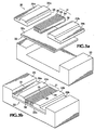
- Pumpendiodeneinheit (10) für einen diodengepumpten Laser, wobei die Einheit folgendes umfasst:ein Substrat (12), das eine Vertiefung (18) definiert, wobei das Substrat (12) zwei Basiselemente (12a, 12b) aufweist, die so konfiguriert sind, dass sie so zusammenpassen, dass zwei Seiten und ein Boden der Vertiefung (18) gebildet werden;eine Mehrzahl von Diodenbarren (14), die in der Vertiefung (18) angeordnet sind; undeine Mehrzahl von wärmeleitfähigen Abstandshaltern (16), die in der Vertiefung (18) angeordnet sind und die Diodenbarren (14) voneinander trennen.
- Pumpendiodeneinheit nach Anspruch 1, wobei es sich bei der Vertiefung (18) um eine im Wesentlichen rechteckige Kerbe handelt, und wobei die Diodenbarren (14) und die Abstandshalter (16) im Wesentlichen rechteckig und so bemessen sind, dass sie in die Kerbe passen.
- Pumpendiodeneinheit nach Anspruch 1, wobei die Basiselemente (12a, 12b) so konfiguriert sind, dass sie eine Klemmkraft auf die Diodenbarren (14) und die Abstandshalter (16) ausüben.
- Pumpendiodeneinheit nach Anspruch 1, wobei die Basiselemente, welche die beiden Seiten der Vertiefung (12a, 12b) bilden, aus einem Material bestehen, das aus der Gruppe ausgewählt wird, die folgendes umfasst: Berylliumoxid, Aluminiumoxid, Aluminiumnitrid und Diamant.
- Pumpendiodeneinheit nach Anspruch 1, wobei die Abstandshalter (16) aus einem Material mit hoher Wärmeleitfähigkeit bestehen, das aus der Gruppe ausgewählt wird, die folgendes umfasst: Gold, Kupfer, Kupfer-Wolfram-Legierung, Saphir, Berylliumoxid und Diamant.
- Pumpendiodeneinheit nach Anspruch 5, wobei die Abstandshalter (16) mit einem metallischen Lötmittel überzogen sind, um einen elektrisch leitfähigen Pfad zwischen den Diodenbarren (14) und den Abstandshaltern (16) bereitzustellen.
- Pumpendiodeneinheit nach Anspruch 1, wobei diese ferner folgendes umfasst:mindestens einen optischen Wärmeverteiler (62), der zwischen einer Lasermediumplatte (60) und den Diodenbarren (14) angeordnet ist, wobei der optische Wärmeverteiler (62) so konfiguriert ist, dass er eine substanzielle Übermittlung der von den Diodenbarren (14) zu der Platte (60) ermöglicht.
- Pumpenkopfeinheit (49) für einen diodengepumpten Laser, wobei die Einheit folgendes umfasst:eine Pumpendiodeneinheit (10) nach Anspruch 1 oder Anspruch 7, wobei es sich bei der Vertiefung (18) um eine im Wesentlichen planare Vertiefung (58) handelt, und wobei die Pumpenkopfeinheit (49) ferner folgendes umfasst:eine Lasermediumplatte (60);mindestens einen Wärmeverteiler (62), der so konfiguriert ist, dass er Wärme von der Lasermediumplatte (60) weg leitet und die Übermittlung von Strahlung von den Diodenbarren (54) zu der Lasermediumplatte (60) ermöglicht; undeine wärmeleitfähige Basis (67) zum sicheren Anbringen des Substrats (52), der Diodenbarren (54), der Abstandshalter (56), der Lasermediumplatte (60) und des Wärmeverteilers (62).
- Pumpenkopfeinheit nach Anspruch 8, wobei die Diodenbarren (54) und die Abstandshalter (56) elongiert sind und in der Vertiefung (58) in einer im Wesentlichen parallelen und alternierenden Anordnung angeordnet sind.
- Pumpenkopfeinheit nach Anspruch 8, wobei diese ferner die in Anspruch 2 oder Anspruch 3 aufgeführten Merkmale umfasst.
- Pumpenkopfeinheit nach Anspruch 8, wobei der optische Wärmeverteiler (62) zwischen der Lasermediumplatte (60) und den Diodenbarren (54) und angrenzend daran angeordnet ist.
- Vierfach symmetrische Pumpenkopfeinheit (100) für einen diodengepumpten Laser, mit ersten, zweiten, dritten und vierten Pumpendiodeneinheiten (110) gemäß der Definition in Anspruch 1 oder Anspruch 7, wobei die ersten und zweiten Pumpendiodeneinheiten (110) im Wesentlichen orthogonal zueinander ausgerichtet sind, und wobei die dritten und vierten Pumpendiodeneinheiten (110) entsprechend im Wesentlichen parallel zu den ersten und zweiten Pumpendiodeneinheiten (110) ausgerichtet sind.
- Vierfach symmetrische Pumpenkopfeinheit nach Anspruch 12, wobei diese ferner erste, zweite, dritte und vierte optische Wärmeverteiler (122) umfasst, die entsprechend angrenzend an die ersten, zweiten, dritten und vierten Pumpendiodeneinheiten (110) angeordnet sind.
- Vierfach symmetrische Pumpenkopfeinheit nach Anspruch 13, wobei diese ferner eine Lasermediumplatte (120) mit vier Seiten umfasst, wobei jede Seite an einen der optischen Wärmeverteiler (122) angrenzt, wobei die optischen Wärmeverteiler (122) jeweils so konfiguriert sind, dass sie Wärme von der Lasermediumplatte (120) weg leiten und eine substanzielle Übermittlung von Strahlung von einem der Diodenbarren (114) zu der Lasermediumplatte (120) ermöglichen, und wobei die Pumpendiodeneinheiten (110) sequentiell entlang einer Längsachse der Platte (120) angeordnet sind und sic' im Wesentlichen nicht überlappen.
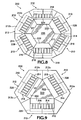
- N-fach symmetrische Pumpenkopfeinheit (200) für einen diodengepumpten Laser, mit einer Mehrzahl von Pumpendiodeneinheiten (210) nach Anspruch 1, wobei mindestens eine Pumpendiodeneinheit (210) im Wesentlichen parallel zu jeder Seite eines N-seitigen, nicht rechteckigen, regelmäßigen Polygons ausgerichtet ist.
- N-fach symmetrische Pumpenkopfeinheit nach Anspruch 15, wobei die Pumpendiodeneinheiten (210) jeweils ein Substrat (212) aufweisen, das eine im Wesentlichen planare Vertiefung (218) definiert und einen wärmeleitfähiges Diamant-Abstandshalter aufweist, der einen Boden der Vertiefung definiert, wobei eine Mehrzahl von Diodenbarren (214) in der Vertiefung (218) angeordnet ist, und wobei eine Mehrzahl von wärmeleitefähigen Abstandshaltern (216) in der Vertiefung (218) angeordnet ist und die Diodenbarren (214) voneinander trennt.
Applications Claiming Priority (1)
| Application Number | Priority Date | Filing Date | Title |
|---|---|---|---|
| PCT/US2006/047448 WO2008073085A2 (en) | 2006-12-12 | 2006-12-12 | Scalable thermally efficient pump diode systems |
Publications (3)
| Publication Number | Publication Date |
|---|---|
| EP2102949A2 EP2102949A2 (de) | 2009-09-23 |
| EP2102949A4 EP2102949A4 (de) | 2010-01-20 |
| EP2102949B1 true EP2102949B1 (de) | 2011-08-10 |
Family
ID=39512222
Family Applications (1)
| Application Number | Title | Priority Date | Filing Date |
|---|---|---|---|
| EP06845311A Not-in-force EP2102949B1 (de) | 2006-12-12 | 2006-12-12 | Skalierbare thermisch effiziente pumpdiodensysteme |
Country Status (5)
| Country | Link |
|---|---|
| EP (1) | EP2102949B1 (de) |
| CN (1) | CN101689744B (de) |
| AT (1) | ATE520177T1 (de) |
| GB (1) | GB2458409A (de) |
| WO (1) | WO2008073085A2 (de) |
Families Citing this family (7)
| Publication number | Priority date | Publication date | Assignee | Title |
|---|---|---|---|---|
| US8964805B2 (en) | 2009-03-12 | 2015-02-24 | Futurewei Technologies, Inc. | Thermally optimized mechanical interface for hybrid integrated wavelength division multiplexed arrayed transmitter |
| CN103457151B (zh) * | 2013-08-08 | 2016-01-20 | 中国科学院苏州生物医学工程技术研究所 | 一种高温硬焊料准连续半导体激光器巴条叠阵封装方法 |
| CN105226485B (zh) * | 2015-10-23 | 2019-03-29 | 惠州市杰普特电子技术有限公司 | 激光散热装置 |
| CN110350395A (zh) * | 2019-07-23 | 2019-10-18 | 长春理工大学 | 一种半导体激光器传导冷却封装结构传导冷却封装结构 |
| CN216134092U (zh) * | 2021-05-12 | 2022-03-25 | 张宝刚 | 一种固态脉冲铥激光和绿激光协同输出的医用激光器 |
| JP7811874B2 (ja) * | 2022-03-29 | 2026-02-06 | 浜松ホトニクス株式会社 | レーザモジュール |
| CN116646816B (zh) * | 2023-05-05 | 2025-05-09 | 西安炬光科技股份有限公司 | 光源组件及半导体激光器 |
Family Cites Families (10)
| Publication number | Priority date | Publication date | Assignee | Title |
|---|---|---|---|---|
| US4306278A (en) * | 1975-09-24 | 1981-12-15 | Grumman Aerospace Corporation | Semiconductor laser array |
| DE19518177A1 (de) * | 1995-05-19 | 1996-11-21 | Fraunhofer Ges Forschung | Diodenlasergepumpter Festkörperlaser |
| US5778020A (en) * | 1996-06-04 | 1998-07-07 | Cj Laser, Inc. | ND: YAG laser pump head |
| US6295307B1 (en) * | 1997-10-14 | 2001-09-25 | Decade Products, Inc. | Laser diode assembly |
| US5913108A (en) * | 1998-04-30 | 1999-06-15 | Cutting Edge Optronics, Inc. | Laser diode packaging |
| CA2284946A1 (en) * | 1999-10-04 | 2001-04-04 | Institut National D'optique | Laser diode array assembly made from a ridged monolithic substrate |
| JPWO2003001634A1 (ja) * | 2001-06-21 | 2004-10-14 | 三菱電機株式会社 | 励起モジュール、レーザ発振器およびレーザ増幅器 |
| US6724792B2 (en) * | 2002-09-12 | 2004-04-20 | The Boeing Company | Laser diode arrays with replaceable laser diode bars and methods of removing and replacing laser diode bars |
| JP2004207496A (ja) * | 2002-12-25 | 2004-07-22 | Nec Corp | 固体レーザ発振器 |
| US7116690B2 (en) * | 2004-05-17 | 2006-10-03 | Textron Systems Corporation | Staggered array coupler |
-
2006
- 2006-12-12 CN CN2006800569092A patent/CN101689744B/zh active Active
- 2006-12-12 EP EP06845311A patent/EP2102949B1/de not_active Not-in-force
- 2006-12-12 AT AT06845311T patent/ATE520177T1/de not_active IP Right Cessation
- 2006-12-12 WO PCT/US2006/047448 patent/WO2008073085A2/en not_active Ceased
- 2006-12-12 GB GB0911913A patent/GB2458409A/en not_active Withdrawn
Also Published As
| Publication number | Publication date |
|---|---|
| ATE520177T1 (de) | 2011-08-15 |
| CN101689744B (zh) | 2012-11-07 |
| EP2102949A2 (de) | 2009-09-23 |
| CN101689744A (zh) | 2010-03-31 |
| EP2102949A4 (de) | 2010-01-20 |
| GB0911913D0 (en) | 2009-08-19 |
| WO2008073085A3 (en) | 2009-01-15 |
| GB2458409A (en) | 2009-09-23 |
| WO2008073085A2 (en) | 2008-06-19 |
Similar Documents
| Publication | Publication Date | Title |
|---|---|---|
| US20090274189A1 (en) | Scalable thermally efficient pump diode systems | |
| US20110069731A1 (en) | Scalable thermally efficient pump diode assemblies | |
| EP1454386B1 (de) | Laser mit einem verteilten verstärkungsmedium | |
| US9246299B2 (en) | Slab laser and amplifier | |
| US5774488A (en) | Solid-state laser with trapped pump light | |
| US7430231B2 (en) | Vertical cavity surface emitting laser (VCSEL) arrays pumped solid-state lasers | |
| US5351251A (en) | Laser apparatus | |
| US6834070B2 (en) | Edge-facet pumped, multi-aperture, thin-disk laser geometry for very high average power output scaling | |
| US7522651B2 (en) | Solid-state lasers employing incoherent monochromatic pump | |
| WO2010145855A1 (en) | Monolithic, side pumped solid-state laser and method for operating the same | |
| WO2005117218A1 (en) | Staggered array coupler | |
| EP2102949B1 (de) | Skalierbare thermisch effiziente pumpdiodensysteme | |
| KR101809429B1 (ko) | 형광 광원 장치 | |
| Shen et al. | Design and development of a high-performance LED-side-pumped Nd: YAG rod laser | |
| AU609050B2 (en) | Frequency shifted laser transmitter | |
| US7949022B2 (en) | Diode pumping of a laser gain medium | |
| TW200415612A (en) | Multiple-disk laser system | |
| EP1788672A2 (de) | Laser mit einem verteilten Verstärkungsmedium | |
| WO2006085886A1 (en) | Solid-state lasers employing incoherent monochromatic pump | |
| Wilson et al. | XeF excimer pumping of Nd: P5O14 | |
| Zhang et al. | Power scaling of Tm: YAG slab ceramic laser | |
| KR20090038223A (ko) | 레이저 발생 장치 및 이의 제조 방법 |
Legal Events
| Date | Code | Title | Description |
|---|---|---|---|
| PUAI | Public reference made under article 153(3) epc to a published international application that has entered the european phase |
Free format text: ORIGINAL CODE: 0009012 |
|
| 17P | Request for examination filed |
Effective date: 20090709 |
|
| AK | Designated contracting states |
Kind code of ref document: A2 Designated state(s): AT BE BG CH CY CZ DE DK EE ES FI FR GB GR HU IE IS IT LI LT LU LV MC NL PL PT RO SE SI SK TR |
|
| A4 | Supplementary search report drawn up and despatched |
Effective date: 20091217 |
|
| DAX | Request for extension of the european patent (deleted) | ||
| 17Q | First examination report despatched |
Effective date: 20100331 |
|
| GRAP | Despatch of communication of intention to grant a patent |
Free format text: ORIGINAL CODE: EPIDOSNIGR1 |
|
| RIC1 | Information provided on ipc code assigned before grant |
Ipc: H01S 5/40 20060101ALI20101014BHEP Ipc: H01S 3/06 20060101ALI20101014BHEP Ipc: H01S 3/0941 20060101AFI20101014BHEP |
|
| GRAS | Grant fee paid |
Free format text: ORIGINAL CODE: EPIDOSNIGR3 |
|
| GRAA | (expected) grant |
Free format text: ORIGINAL CODE: 0009210 |
|
| AK | Designated contracting states |
Kind code of ref document: B1 Designated state(s): AT BE BG CH CY CZ DE DK EE ES FI FR GB GR HU IE IS IT LI LT LU LV MC NL PL PT RO SE SI SK TR |
|
| REG | Reference to a national code |
Ref country code: GB Ref legal event code: FG4D |
|
| REG | Reference to a national code |
Ref country code: CH Ref legal event code: EP |
|
| REG | Reference to a national code |
Ref country code: IE Ref legal event code: FG4D |
|
| REG | Reference to a national code |
Ref country code: DE Ref legal event code: R096 Ref document number: 602006023763 Country of ref document: DE Effective date: 20111013 |
|
| REG | Reference to a national code |
Ref country code: NL Ref legal event code: VDEP Effective date: 20110810 |
|
| LTIE | Lt: invalidation of european patent or patent extension |
Effective date: 20110810 |
|
| PG25 | Lapsed in a contracting state [announced via postgrant information from national office to epo] |
Ref country code: PT Free format text: LAPSE BECAUSE OF FAILURE TO SUBMIT A TRANSLATION OF THE DESCRIPTION OR TO PAY THE FEE WITHIN THE PRESCRIBED TIME-LIMIT Effective date: 20111212 Ref country code: FI Free format text: LAPSE BECAUSE OF FAILURE TO SUBMIT A TRANSLATION OF THE DESCRIPTION OR TO PAY THE FEE WITHIN THE PRESCRIBED TIME-LIMIT Effective date: 20110810 Ref country code: IS Free format text: LAPSE BECAUSE OF FAILURE TO SUBMIT A TRANSLATION OF THE DESCRIPTION OR TO PAY THE FEE WITHIN THE PRESCRIBED TIME-LIMIT Effective date: 20111210 Ref country code: LT Free format text: LAPSE BECAUSE OF FAILURE TO SUBMIT A TRANSLATION OF THE DESCRIPTION OR TO PAY THE FEE WITHIN THE PRESCRIBED TIME-LIMIT Effective date: 20110810 Ref country code: SE Free format text: LAPSE BECAUSE OF FAILURE TO SUBMIT A TRANSLATION OF THE DESCRIPTION OR TO PAY THE FEE WITHIN THE PRESCRIBED TIME-LIMIT Effective date: 20110810 Ref country code: NL Free format text: LAPSE BECAUSE OF FAILURE TO SUBMIT A TRANSLATION OF THE DESCRIPTION OR TO PAY THE FEE WITHIN THE PRESCRIBED TIME-LIMIT Effective date: 20110810 |
|
| REG | Reference to a national code |
Ref country code: AT Ref legal event code: MK05 Ref document number: 520177 Country of ref document: AT Kind code of ref document: T Effective date: 20110810 |
|
| PG25 | Lapsed in a contracting state [announced via postgrant information from national office to epo] |
Ref country code: GR Free format text: LAPSE BECAUSE OF FAILURE TO SUBMIT A TRANSLATION OF THE DESCRIPTION OR TO PAY THE FEE WITHIN THE PRESCRIBED TIME-LIMIT Effective date: 20111111 Ref country code: PL Free format text: LAPSE BECAUSE OF FAILURE TO SUBMIT A TRANSLATION OF THE DESCRIPTION OR TO PAY THE FEE WITHIN THE PRESCRIBED TIME-LIMIT Effective date: 20110810 Ref country code: AT Free format text: LAPSE BECAUSE OF FAILURE TO SUBMIT A TRANSLATION OF THE DESCRIPTION OR TO PAY THE FEE WITHIN THE PRESCRIBED TIME-LIMIT Effective date: 20110810 Ref country code: CY Free format text: LAPSE BECAUSE OF FAILURE TO SUBMIT A TRANSLATION OF THE DESCRIPTION OR TO PAY THE FEE WITHIN THE PRESCRIBED TIME-LIMIT Effective date: 20110810 Ref country code: SI Free format text: LAPSE BECAUSE OF FAILURE TO SUBMIT A TRANSLATION OF THE DESCRIPTION OR TO PAY THE FEE WITHIN THE PRESCRIBED TIME-LIMIT Effective date: 20110810 Ref country code: LV Free format text: LAPSE BECAUSE OF FAILURE TO SUBMIT A TRANSLATION OF THE DESCRIPTION OR TO PAY THE FEE WITHIN THE PRESCRIBED TIME-LIMIT Effective date: 20110810 |
|
| PG25 | Lapsed in a contracting state [announced via postgrant information from national office to epo] |
Ref country code: BE Free format text: LAPSE BECAUSE OF FAILURE TO SUBMIT A TRANSLATION OF THE DESCRIPTION OR TO PAY THE FEE WITHIN THE PRESCRIBED TIME-LIMIT Effective date: 20110810 |
|
| PG25 | Lapsed in a contracting state [announced via postgrant information from national office to epo] |
Ref country code: SK Free format text: LAPSE BECAUSE OF FAILURE TO SUBMIT A TRANSLATION OF THE DESCRIPTION OR TO PAY THE FEE WITHIN THE PRESCRIBED TIME-LIMIT Effective date: 20110810 Ref country code: CZ Free format text: LAPSE BECAUSE OF FAILURE TO SUBMIT A TRANSLATION OF THE DESCRIPTION OR TO PAY THE FEE WITHIN THE PRESCRIBED TIME-LIMIT Effective date: 20110810 |
|
| PG25 | Lapsed in a contracting state [announced via postgrant information from national office to epo] |
Ref country code: RO Free format text: LAPSE BECAUSE OF FAILURE TO SUBMIT A TRANSLATION OF THE DESCRIPTION OR TO PAY THE FEE WITHIN THE PRESCRIBED TIME-LIMIT Effective date: 20110810 Ref country code: EE Free format text: LAPSE BECAUSE OF FAILURE TO SUBMIT A TRANSLATION OF THE DESCRIPTION OR TO PAY THE FEE WITHIN THE PRESCRIBED TIME-LIMIT Effective date: 20110810 Ref country code: IT Free format text: LAPSE BECAUSE OF FAILURE TO SUBMIT A TRANSLATION OF THE DESCRIPTION OR TO PAY THE FEE WITHIN THE PRESCRIBED TIME-LIMIT Effective date: 20110810 |
|
| PLBE | No opposition filed within time limit |
Free format text: ORIGINAL CODE: 0009261 |
|
| STAA | Information on the status of an ep patent application or granted ep patent |
Free format text: STATUS: NO OPPOSITION FILED WITHIN TIME LIMIT |
|
| PG25 | Lapsed in a contracting state [announced via postgrant information from national office to epo] |
Ref country code: DK Free format text: LAPSE BECAUSE OF FAILURE TO SUBMIT A TRANSLATION OF THE DESCRIPTION OR TO PAY THE FEE WITHIN THE PRESCRIBED TIME-LIMIT Effective date: 20110810 |
|
| 26N | No opposition filed |
Effective date: 20120511 |
|
| PG25 | Lapsed in a contracting state [announced via postgrant information from national office to epo] |
Ref country code: MC Free format text: LAPSE BECAUSE OF NON-PAYMENT OF DUE FEES Effective date: 20111231 |
|
| REG | Reference to a national code |
Ref country code: CH Ref legal event code: PL |
|
| REG | Reference to a national code |
Ref country code: DE Ref legal event code: R097 Ref document number: 602006023763 Country of ref document: DE Effective date: 20120511 |
|
| REG | Reference to a national code |
Ref country code: IE Ref legal event code: MM4A |
|
| PG25 | Lapsed in a contracting state [announced via postgrant information from national office to epo] |
Ref country code: LI Free format text: LAPSE BECAUSE OF NON-PAYMENT OF DUE FEES Effective date: 20111231 Ref country code: IE Free format text: LAPSE BECAUSE OF NON-PAYMENT OF DUE FEES Effective date: 20111212 Ref country code: CH Free format text: LAPSE BECAUSE OF NON-PAYMENT OF DUE FEES Effective date: 20111231 |
|
| PG25 | Lapsed in a contracting state [announced via postgrant information from national office to epo] |
Ref country code: ES Free format text: LAPSE BECAUSE OF FAILURE TO SUBMIT A TRANSLATION OF THE DESCRIPTION OR TO PAY THE FEE WITHIN THE PRESCRIBED TIME-LIMIT Effective date: 20111121 |
|
| PG25 | Lapsed in a contracting state [announced via postgrant information from national office to epo] |
Ref country code: LU Free format text: LAPSE BECAUSE OF NON-PAYMENT OF DUE FEES Effective date: 20111212 |
|
| PG25 | Lapsed in a contracting state [announced via postgrant information from national office to epo] |
Ref country code: BG Free format text: LAPSE BECAUSE OF FAILURE TO SUBMIT A TRANSLATION OF THE DESCRIPTION OR TO PAY THE FEE WITHIN THE PRESCRIBED TIME-LIMIT Effective date: 20111110 |
|
| PGFP | Annual fee paid to national office [announced via postgrant information from national office to epo] |
Ref country code: DE Payment date: 20130624 Year of fee payment: 7 Ref country code: GB Payment date: 20130610 Year of fee payment: 7 |
|
| PGFP | Annual fee paid to national office [announced via postgrant information from national office to epo] |
Ref country code: FR Payment date: 20130703 Year of fee payment: 7 |
|
| PG25 | Lapsed in a contracting state [announced via postgrant information from national office to epo] |
Ref country code: TR Free format text: LAPSE BECAUSE OF FAILURE TO SUBMIT A TRANSLATION OF THE DESCRIPTION OR TO PAY THE FEE WITHIN THE PRESCRIBED TIME-LIMIT Effective date: 20110810 |
|
| PG25 | Lapsed in a contracting state [announced via postgrant information from national office to epo] |
Ref country code: HU Free format text: LAPSE BECAUSE OF FAILURE TO SUBMIT A TRANSLATION OF THE DESCRIPTION OR TO PAY THE FEE WITHIN THE PRESCRIBED TIME-LIMIT Effective date: 20110810 |
|
| REG | Reference to a national code |
Ref country code: DE Ref legal event code: R119 Ref document number: 602006023763 Country of ref document: DE |
|
| GBPC | Gb: european patent ceased through non-payment of renewal fee |
Effective date: 20131212 |
|
| REG | Reference to a national code |
Ref country code: DE Ref legal event code: R119 Ref document number: 602006023763 Country of ref document: DE Effective date: 20140701 |
|
| REG | Reference to a national code |
Ref country code: FR Ref legal event code: ST Effective date: 20140829 |
|
| PG25 | Lapsed in a contracting state [announced via postgrant information from national office to epo] |
Ref country code: DE Free format text: LAPSE BECAUSE OF NON-PAYMENT OF DUE FEES Effective date: 20140701 |
|
| PG25 | Lapsed in a contracting state [announced via postgrant information from national office to epo] |
Ref country code: FR Free format text: LAPSE BECAUSE OF NON-PAYMENT OF DUE FEES Effective date: 20131231 Ref country code: GB Free format text: LAPSE BECAUSE OF NON-PAYMENT OF DUE FEES Effective date: 20131212 |