EP2102748B1 - Système et procédé de récupération de transactions de mémoire - Google Patents
Système et procédé de récupération de transactions de mémoire Download PDFInfo
- Publication number
- EP2102748B1 EP2102748B1 EP07826951A EP07826951A EP2102748B1 EP 2102748 B1 EP2102748 B1 EP 2102748B1 EP 07826951 A EP07826951 A EP 07826951A EP 07826951 A EP07826951 A EP 07826951A EP 2102748 B1 EP2102748 B1 EP 2102748B1
- Authority
- EP
- European Patent Office
- Prior art keywords
- transaction
- valid
- marker
- writing
- recovery
- Prior art date
- Legal status (The legal status is an assumption and is not a legal conclusion. Google has not performed a legal analysis and makes no representation as to the accuracy of the status listed.)
- Not-in-force
Links
Images


Classifications
-
- G—PHYSICS
- G06—COMPUTING; CALCULATING OR COUNTING
- G06F—ELECTRIC DIGITAL DATA PROCESSING
- G06F11/00—Error detection; Error correction; Monitoring
- G06F11/07—Responding to the occurrence of a fault, e.g. fault tolerance
- G06F11/14—Error detection or correction of the data by redundancy in operation
- G06F11/1402—Saving, restoring, recovering or retrying
- G06F11/1415—Saving, restoring, recovering or retrying at system level
- G06F11/1441—Resetting or repowering
-
- G—PHYSICS
- G06—COMPUTING; CALCULATING OR COUNTING
- G06F—ELECTRIC DIGITAL DATA PROCESSING
- G06F11/00—Error detection; Error correction; Monitoring
- G06F11/07—Responding to the occurrence of a fault, e.g. fault tolerance
- G06F11/14—Error detection or correction of the data by redundancy in operation
- G06F11/1402—Saving, restoring, recovering or retrying
- G06F11/1405—Saving, restoring, recovering or retrying at machine instruction level
- G06F11/141—Saving, restoring, recovering or retrying at machine instruction level for bus or memory accesses
Definitions
- the present invention is related to a method for transactional writing of data into a persistent memory.
- the invention is further related to a corresponding memory system and a corresponding computer program.
- a transition from one consistent memory system state to another may involve updates of several memory cells of persistent memory. These updates should be performed atomically, that means either all memory cells are updated or none of them.
- the atomicity of several memory updates is supported by the so called “transaction model" in which the system can designate the beginning of an atomic set of updates by issuing the begin-of-transaction command. This command may be given explicitly or even implicitly, i.e. be contained in the atomic set command itself. For instance primitive commands, like the data types "byte” and "short” have to be atomically updated and their mere appearance may already serve as begin-of-transaction command. After this point, each persistent memory cell is updated only conditionally by a transaction support system.
- Memory systems such as smart cards may be equipped with different types of persistent read/write memory, some of which (such as EEPROM) exhibit the behaviour of so-called “weak cells". These weak cells are created when, during writing the memory cells, the smart card is removed from the smart card reader and therefore cannot fully complete the write operation before being cut off from its power supply. In the following, this is called a "weak write”. After reboot, the weak memory cell then may not only return any value but even different values at different times, e.g., if read more than once. This may seriously harm the functionality of the smart card.
- Oestreicher describes in "Transactions in Java Card", Computer Security Applications Conference 1999, AZ, USA, 6-10 Dec. 1999 a transaction model implied by the Java Card 2.1 specifications and presents a detailed discussion of possible implementation schemes and their optimization.
- the present invention is directed to a method, a memory system and a computer program as defined in independent claims. Further embodiments of the invention are provided in the appended dependent claims.
- a method for transactional writing of data into a persistent memory comprising memory cells, the method comprising a transactional writing step and a transaction recovery step,
- a transaction recovery marker that indicates the start of a transaction recovery allows an evaluation whether a former transaction recovery was aborted.
- the transaction recovery marker indicates a pending transaction recovery.
- a memory system can check upon starting of a transaction recovery, if the respective transaction buffer comprises data from a former transaction recovery that could not be completed. This information about former and not completed transaction recoveries can be used to improve and enhance the reliability of the transaction recovery of memory systems. It is in particular useful to provide measures for avoiding memory system failures caused by weak writes.
- the transaction buffer comprises two functions. On the one hand it indicates a pending transaction recovery and on the other hand it indicates the last valid transaction buffer entry. This is very efficient in terms of reducing writing steps to the transaction buffer.
- a valid transaction recovery marker is defined by a predefined bit pattern.
- This embodiment is in particular useful for memory cells for which after a weak write all possible combinations of data values for the respective weakly written memory cell arise with the same probability.
- it is in particular useful for memories cells for which it can be assumed that after a weak write all data values are equally distributed.
- the probability that the transaction recovery marker is weakly written can be chosen by the size of the transaction recovery marker. The longer the transaction recovery marker, the lower the chance that the predefined bit pattern of the transaction recovery marker is by accident written by a weak write.
- n denotes the number of bits of the transaction recovery marker.
- the predefined bit pattern according to this embodiment of the invention is a bit pattern of zeros.
- a valid transaction recovery marker would be defined by any bit pattern that does not only comprise zeros.
- the first valid marker is defined by a predefined bit pattern.
- Providing a first and a second valid marker provides redundancy and allows validity checking in pairs. By such validity checking in pairs the validity of one value can be derived from the validity of the other value.
- the first valid marker serves as validity indicator for the second valid marker. If the first valid marker is read as valid, it can be assumed that the previously written second valid marker was completely written and is not a weak-write.
- the transaction recovery step further comprises a rewriting step for rewriting the first valid marker of the first transaction buffer entry, the rewriting step being performed after the transaction buffer checking step if the first valid marker of the first transaction buffer entry is valid.
- a computer program for transactional writing of data into a memory device comprising instructions for carrying out the steps of the method according to the first aspect of the invention when said computer program is executed on a memory system.
- any of the device features may be applied to the method aspect of the invention and vice versa. Advantages of the device features apply to corresponding method features and vice versa.
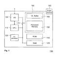
- the memory system 100 writes the current data value of the respective memory cell and the corresponding address as transaction buffer entry in the transaction buffer 160.
- the memory system 100 writes a second valid marker for the transaction buffer entry in the transaction buffer 160.
- the memory system 100 writes a first valid marker for the transaction buffer entry in the transaction buffer 160.
- the sub-step 230 is optional and may be omitted for some embodiments of the invention. If the sub-step 230 is omitted, there is only one valid marker, namely the first valid marker, written in the transaction buffer 160. As an alternative, bits or bytes that are present in a transaction buffer entry anyway can be used as second valid marker.
- Fig. 4 shows a block diagram of a transaction buffer 400 according to another exemplary embodiment of the invention.
- the transaction buffer 400 comprises transaction buffer entries 401.
- the transaction buffer 400 may comprise any number of transaction buffer entries which is indicated by the bolded points.
- Each of the transaction buffer entries 401 comprises a first valid marker M 1 denoted by the reference numeral 402.
- the first valid marker M 1 is preferably defined as valid by a predefined bit pattern.
- each of the transaction buffer entries 401 comprises data fields 403 comprising a data value and the corresponding address of the data value in the persistent memory 150.
- the first valid markers M 1 indicate that the corresponding data fields 403 comprise a valid data value and data address.
- the transaction buffer 400 comprises a transaction recovery marker 405.
- the transaction recovery marker 405 should preferably comprise more bits or bytes respectively than the page size of the memory system 100.
- a preferred size of the transaction recovery marker 405 could be e.g. 64 bytes.
- the size of the transaction recovery marker 405 determines the probability that a weakly written transaction recovery marker 405 is read as valid. Under the assumption that after a weak write all possible bit combinations of the transaction recovery marker 405 that comprises n-bits are equally distributed, i.e. occur with the same probability, the chance is only 1/(2 ⁇ n) that a transaction recovery marker 405 that has been written as valid stems from a weak-write. So if actually a valid transaction recovery marker 405 is read, it may be considered as not written weakly in the beginning and it may be assumed that it is stable and will not change its value.
- the transaction recovery step 700 as illustrated in Fig. 7 is in particular suited for persistent memories that exhibit the following properties: It can be assumed that after a weak write it is more likely to actually read the weakly written data value for a period of time, in particular a short period of time, before the contents of the affected memory cells may arbitrarily change their data values.
- sub-step 720 If in sub-step 720 the first valid marker M 1* of the first transaction buffer entry 501 * is not valid, the transaction recovery step 700 continues with a sub-step 810 which starts the subroutine 800. In a following sub-step 820 it is checked whether the transaction recovery marker 505 is invalid as well. If this is the case, the subroutine 800 stops in an ending sub-step 825. Actually this indicates that there was previously no aborted transaction recovery. If the result of sub-step 820 is that the transaction recovery marker 505 is valid, this indicates that the restoring sub-step 750 of the transaction recovery step 700 could be completed, but that the sub-steps 760 and/or 770 could not be completed.
Claims (10)
- Procédé d'écriture transactionnelle de données dans une mémoire persistante de carte à puce qui comprend des cellules de mémoire, ledit procédé comprenant une étape d'écriture transactionnelle et une étape de récupération de transactions,- l'étape d'écriture transactionnelle comprenant une ou deux étapes d'écriture de cellule de mémoire, les étapes d'écriture de cellule de mémoire comprenant la séquence suivante d'étapes secondaires :a.) écriture de la valeur de données courante et de l'adresse correspondante de la cellule de mémoire respective dans un tampon de transaction en tant qu'entrée de tampon de transaction,b.) écriture d'un premier marqueur valide pour la cellule de mémoire dans le tampon de transaction,c.) écriture d'une nouvelle valeur de données dans la cellule de mémoire ;- l'étape de récupération de transactions intervenant en cas d'un abandon de l'étape d'écriture transactionnelle et permettant de restaurer les valeurs de données courantes de la transaction abandonnée dans la mémoire persistante, l'étape de récupération de transaction comprenant la séquence suivante d'étapes secondaires :a.) une étape de vérification du tampon de transaction pour vérifier si le premier marqueur valide de la première entrée du tampon de transaction est valide ;b.) si le premier marqueur valide de la première entrée du tampon de transaction est valide, une étape de vérification du marqueur de récupération de transaction pour vérifier si le marqueur de récupération de transaction est valide ;c.) si le marqueur de récupération de transaction n'est pas valide, écriture d'un marqueur de récupération de transaction dans le tampon de transaction pour indiquer le démarrage de la récupération de transactions, dans laquelle le marqueur de récupération de transaction est écrit derrière la dernière entrée valide du tampon de transaction,d.) restauration de toutes les entrées du tampon de transaction jusqu'au marqueur de récupération de transaction dans la mémoire persistante ;e.) invalidation du premier marqueur valide du tampon de transaction,f.) invalidation du marqueur de récupération de transaction.
- Procédé selon la revendication 1, dans lequel un marqueur valide de récupération de transaction est défini par une configuration binaire prédéfinie.
- Procédé selon la revendication 1, dans lequel un marqueur valide de récupération de transaction est défini par une configuration binaire non égale à la configuration binaire prédéfinie.
- Procédé selon l'une quelconque des revendications précédentes, dans lequel le premier marqueur valide est défini par une configuration binaire prédéfinie.
- Procédé selon l'une quelconque des revendications précédentes, dans lequel l'étape d'écriture transactionnelle comprend l'écriture d'un second marqueur valide avant celle du premier marqueur valide.
- Procédé selon la revendication 5, dans lequel le second marqueur valide est défini par une configuration binaire non égale à la configuration binaire prédéfinie.
- Procédé selon la revendication 1, dans lequel l'étape de récupération de transaction comprend également une étape de réécriture pour réécrire le premier marqueur valide de la première entrée de tampon de transaction, l'étape de réécriture intervenant après l'étape de vérification du tampon de transaction si le premier marqueur valide de la première entrée de tampon de transaction est valide.
- Procédé selon la revendication 1, comprenant également les étapes suivantes si le premier marqueur valide de la première entrée de tampon de transaction n'est pas valide :- vérifier si le marqueur de récupération de transaction est valide et, si le marqueur de récupération de transaction n'est pas valide, effectuer les étapes- d'invalidation du premier marqueur valide du premier tampon de transaction,- d'invalidation du marqueur de récupération de transaction.
- Carte à puces comprenant une mémoire persistante et un tampon de transaction persistant, la carte à puces servant à l'écriture transactionnelle de valeurs de données dans la mémoire persistante, la carte à puces permettant d'effectuer une étape d'écriture transactionnelle et une étape de récupération de transaction, l'étape d'écriture transactionnelle comprenant une ou plusieurs étapes d'écriture de cellule de mémoire, les étapes d'écriture de cellule de mémoire comprenant la séquence suivante d'étapes secondaires :a.) écriture de la valeur de donnés courante et de l'adresse correspondante de la cellule de mémoire respective dans un tampon de transaction en tant qu'entrée de tampon de transaction,b.) écriture d'un premier marqueur valide pour la cellule de mémoire dans le tampon de transaction,c.) écriture d'une nouvelle valeur de données dans la cellule de mémoire ;- l'étape de récupération de transaction étant exécutée dans le cas d'un abandon de l'étape d'écriture de transaction et permettant de récupérer les valeurs de données courantes de la transaction abandonnée dans la mémoire persistante, l'étape de récupération de transaction comprenant la séquence suivante d'étapes secondaires :a.) étape de vérification du tampon de transaction pour vérifier si le premier marqueur valide de la première entrée du tampon de transaction est valide ;b.) si le premier marqueur valide de la première entrée du tampon de transaction est valide, une étape de vérification du marqueur de récupération de transaction pour vérifier si le marqueur de récupération de transaction est valide ;c.) si le marqueur de récupération de transaction n'est pas valide, écriture d'un marqueur de récupération de transaction dans le tampon de transaction pour indiquer le démarrage de la récupération de transactions, dans laquelle le marqueur de récupération de transaction est écrit derrière la dernière entrée valide du tampon de transaction,d.) restauration de toutes les entrées du tampon de transaction jusqu'au marqueur de récupération de transaction dans la mémoire persistante ;e.) invalidation du premier marqueur valide du tampon de transaction,f.) invalidation du marqueur de récupération de transaction.
- Programme informatique pour l'écriture transactionnelle de données dans une mémoire persistante d'une carte à puce comprenant des instructions permettant de réaliser le procédé selon l'une quelconque des revendications 1 à 8 lorsque ledit programme est exécuté sur la carte à puce.
Priority Applications (1)
| Application Number | Priority Date | Filing Date | Title |
|---|---|---|---|
| EP07826951A EP2102748B1 (fr) | 2006-12-22 | 2007-11-02 | Système et procédé de récupération de transactions de mémoire |
Applications Claiming Priority (3)
| Application Number | Priority Date | Filing Date | Title |
|---|---|---|---|
| EP06127040 | 2006-12-22 | ||
| EP07826951A EP2102748B1 (fr) | 2006-12-22 | 2007-11-02 | Système et procédé de récupération de transactions de mémoire |
| PCT/IB2007/054446 WO2008078207A2 (fr) | 2006-12-22 | 2007-11-02 | Système et procédé de récupération de transactions de mémoire |
Publications (2)
| Publication Number | Publication Date |
|---|---|
| EP2102748A2 EP2102748A2 (fr) | 2009-09-23 |
| EP2102748B1 true EP2102748B1 (fr) | 2012-02-01 |
Family
ID=39511287
Family Applications (1)
| Application Number | Title | Priority Date | Filing Date |
|---|---|---|---|
| EP07826951A Not-in-force EP2102748B1 (fr) | 2006-12-22 | 2007-11-02 | Système et procédé de récupération de transactions de mémoire |
Country Status (4)
| Country | Link |
|---|---|
| US (1) | US7861114B2 (fr) |
| EP (1) | EP2102748B1 (fr) |
| AT (1) | ATE544114T1 (fr) |
| WO (1) | WO2008078207A2 (fr) |
Families Citing this family (4)
| Publication number | Priority date | Publication date | Assignee | Title |
|---|---|---|---|---|
| CU23432B6 (es) * | 2005-11-02 | 2009-10-16 | Ct Ingenieria Genetica Biotech | Formulaciones estabilizadas que contienen a los interferones gamma y alfa en proporciones potenciadoras |
| FR2988878B1 (fr) * | 2012-04-02 | 2015-01-16 | Morpho | Procede de modification en memoire d'un ensemble de donnees |
| US9015404B2 (en) * | 2012-09-28 | 2015-04-21 | Intel Corporation | Persistent log operations for non-volatile memory |
| US10229012B2 (en) * | 2016-08-15 | 2019-03-12 | Oracle International Corporation | Committing copy-on-write transaction with a persist barrier for a persistent object including payload references |
Family Cites Families (9)
| Publication number | Priority date | Publication date | Assignee | Title |
|---|---|---|---|---|
| US4922456A (en) * | 1988-04-29 | 1990-05-01 | Scientific-Atlanta, Inc. | Method of reducing wearout in a non-volatile memory with double buffer |
| DE19600081C2 (de) * | 1996-01-03 | 1999-11-18 | Ibm | Sicherung der Datenintegrität bei Datenträgerkarten |
| EP0831433A1 (fr) * | 1996-09-24 | 1998-03-25 | Koninklijke KPN N.V. | Méthode pour réaliser une transaction récupérable avec une carte à circuit intégré, une méthode pour récupérer une telle transaction ainsi qu'une carte à circuit intégré permettant des transactions récupérables |
| US5988510A (en) * | 1997-02-13 | 1999-11-23 | Micron Communications, Inc. | Tamper resistant smart card and method of protecting data in a smart card |
| US6272607B1 (en) * | 1998-08-28 | 2001-08-07 | International Business Machines Corporation | Method and apparatus for transactional writing of data into a persistent memory |
| US6535997B1 (en) * | 1999-05-19 | 2003-03-18 | International Business Machines Corporation | Data integrity in smartcard transactions |
| US7065538B2 (en) * | 2000-02-11 | 2006-06-20 | Quest Software, Inc. | System and method for reconciling transactions between a replication system and a recovered database |
| KR100390853B1 (ko) * | 2000-06-07 | 2003-07-10 | 차상균 | 주 메모리 트랜잭션 처리 시스템에서 병렬적 회복 연산을 위한 디퍼런셜 로깅 방법 및 장치 |
| DE10141926B4 (de) * | 2001-08-28 | 2004-05-06 | Giesecke & Devrient Gmbh | Verfahren zur Sicherung der Daten eines Datenspeichers |
-
2007
- 2007-11-02 EP EP07826951A patent/EP2102748B1/fr not_active Not-in-force
- 2007-11-02 AT AT07826951T patent/ATE544114T1/de active
- 2007-11-02 WO PCT/IB2007/054446 patent/WO2008078207A2/fr active Application Filing
- 2007-12-21 US US11/962,718 patent/US7861114B2/en active Active
Also Published As
| Publication number | Publication date |
|---|---|
| US20080168307A1 (en) | 2008-07-10 |
| EP2102748A2 (fr) | 2009-09-23 |
| WO2008078207A2 (fr) | 2008-07-03 |
| ATE544114T1 (de) | 2012-02-15 |
| WO2008078207A3 (fr) | 2008-11-20 |
| US7861114B2 (en) | 2010-12-28 |
Similar Documents
| Publication | Publication Date | Title |
|---|---|---|
| US6272607B1 (en) | Method and apparatus for transactional writing of data into a persistent memory | |
| CN106227680B (zh) | 一种数据处理及防掉电数据保护方法 | |
| JP2010072965A (ja) | 携帯可能電子装置および携帯可能電子装置におけるデータ処理方法 | |
| US20070011416A1 (en) | Data storage device and medium and related method of storing backup data | |
| EP2102748B1 (fr) | Système et procédé de récupération de transactions de mémoire | |
| CN101645046A (zh) | 一次性可编程存储器仿真 | |
| CN107402717B (zh) | 闪速存储器存储管理 | |
| US20030120770A1 (en) | Method and apparatus for processing transactions in a data processing system | |
| JP5104653B2 (ja) | Icカード及びicカードプログラム | |
| CN107239229B (zh) | 用于执行数据更新的方法 | |
| JP5754287B2 (ja) | Icチップ、icチップにおける処理方法、uim、携帯端末、及びicチップ用処理プログラム | |
| JP4460850B2 (ja) | Icカードとicカードの処理方法 | |
| JP4195822B2 (ja) | Icカード及びicカードプログラム | |
| CN107402887B (zh) | 闪速存储器中的计数器 | |
| US10461971B2 (en) | IC card, portable electronic device, program, processing apparatus, and processing system | |
| US20070274302A1 (en) | Data Storage Device, Memory Managing Method, and Program | |
| US7346730B2 (en) | Mobile electronic device | |
| JP6252341B2 (ja) | 電子情報記憶媒体、情報処理方法、及び情報処理プログラム | |
| JP6984328B2 (ja) | 電子情報記憶媒体、icカード、外部機器、データ書き込み方法及びデータ書き込みプログラム | |
| US20170185334A1 (en) | Storage in flash memory | |
| CN114637626B (zh) | 减少eeprom数据读写出错的方法、装置、设备及可读存储介质 | |
| CN112558878B (zh) | 一种基于不同类型存储机制的空间调换方法 | |
| JP6758910B2 (ja) | Icカード | |
| JP2016153945A (ja) | 電子情報記憶媒体、カウンタ書換方法、及びカウンタ書換プログラム | |
| CN114253674A (zh) | 一种流处理方法和装置 |
Legal Events
| Date | Code | Title | Description |
|---|---|---|---|
| PUAI | Public reference made under article 153(3) epc to a published international application that has entered the european phase |
Free format text: ORIGINAL CODE: 0009012 |
|
| 17P | Request for examination filed |
Effective date: 20090709 |
|
| AK | Designated contracting states |
Kind code of ref document: A2 Designated state(s): AT BE BG CH CY CZ DE DK EE ES FI FR GB GR HU IE IS IT LI LT LU LV MC MT NL PL PT RO SE SI SK TR |
|
| 17Q | First examination report despatched |
Effective date: 20090929 |
|
| DAX | Request for extension of the european patent (deleted) | ||
| GRAP | Despatch of communication of intention to grant a patent |
Free format text: ORIGINAL CODE: EPIDOSNIGR1 |
|
| GRAS | Grant fee paid |
Free format text: ORIGINAL CODE: EPIDOSNIGR3 |
|
| GRAA | (expected) grant |
Free format text: ORIGINAL CODE: 0009210 |
|
| AK | Designated contracting states |
Kind code of ref document: B1 Designated state(s): AT BE BG CH CY CZ DE DK EE ES FI FR GB GR HU IE IS IT LI LT LU LV MC MT NL PL PT RO SE SI SK TR |
|
| REG | Reference to a national code |
Ref country code: GB Ref legal event code: FG4D |
|
| REG | Reference to a national code |
Ref country code: CH Ref legal event code: EP Ref country code: AT Ref legal event code: REF Ref document number: 544114 Country of ref document: AT Kind code of ref document: T Effective date: 20120215 |
|
| REG | Reference to a national code |
Ref country code: DE Ref legal event code: R084 Ref document number: 602007020475 Country of ref document: DE |
|
| REG | Reference to a national code |
Ref country code: CH Ref legal event code: NV Representative=s name: IBM RESEARCH GMBH ZURICH RESEARCH LABORATORY INTEL |
|
| REG | Reference to a national code |
Ref country code: DE Ref legal event code: R096 Ref document number: 602007020475 Country of ref document: DE Effective date: 20120329 |
|
| REG | Reference to a national code |
Ref country code: GB Ref legal event code: 746 Effective date: 20120416 |
|
| REG | Reference to a national code |
Ref country code: DE Ref legal event code: R084 Ref document number: 602007020475 Country of ref document: DE Effective date: 20120307 |
|
| REG | Reference to a national code |
Ref country code: NL Ref legal event code: VDEP Effective date: 20120201 |
|
| LTIE | Lt: invalidation of european patent or patent extension |
Effective date: 20120201 |
|
| PG25 | Lapsed in a contracting state [announced via postgrant information from national office to epo] |
Ref country code: NL Free format text: LAPSE BECAUSE OF FAILURE TO SUBMIT A TRANSLATION OF THE DESCRIPTION OR TO PAY THE FEE WITHIN THE PRESCRIBED TIME-LIMIT Effective date: 20120201 Ref country code: IS Free format text: LAPSE BECAUSE OF FAILURE TO SUBMIT A TRANSLATION OF THE DESCRIPTION OR TO PAY THE FEE WITHIN THE PRESCRIBED TIME-LIMIT Effective date: 20120601 Ref country code: LT Free format text: LAPSE BECAUSE OF FAILURE TO SUBMIT A TRANSLATION OF THE DESCRIPTION OR TO PAY THE FEE WITHIN THE PRESCRIBED TIME-LIMIT Effective date: 20120201 |
|
| PG25 | Lapsed in a contracting state [announced via postgrant information from national office to epo] |
Ref country code: BE Free format text: LAPSE BECAUSE OF FAILURE TO SUBMIT A TRANSLATION OF THE DESCRIPTION OR TO PAY THE FEE WITHIN THE PRESCRIBED TIME-LIMIT Effective date: 20120201 Ref country code: PT Free format text: LAPSE BECAUSE OF FAILURE TO SUBMIT A TRANSLATION OF THE DESCRIPTION OR TO PAY THE FEE WITHIN THE PRESCRIBED TIME-LIMIT Effective date: 20120601 Ref country code: GR Free format text: LAPSE BECAUSE OF FAILURE TO SUBMIT A TRANSLATION OF THE DESCRIPTION OR TO PAY THE FEE WITHIN THE PRESCRIBED TIME-LIMIT Effective date: 20120502 Ref country code: FI Free format text: LAPSE BECAUSE OF FAILURE TO SUBMIT A TRANSLATION OF THE DESCRIPTION OR TO PAY THE FEE WITHIN THE PRESCRIBED TIME-LIMIT Effective date: 20120201 Ref country code: PL Free format text: LAPSE BECAUSE OF FAILURE TO SUBMIT A TRANSLATION OF THE DESCRIPTION OR TO PAY THE FEE WITHIN THE PRESCRIBED TIME-LIMIT Effective date: 20120201 Ref country code: LV Free format text: LAPSE BECAUSE OF FAILURE TO SUBMIT A TRANSLATION OF THE DESCRIPTION OR TO PAY THE FEE WITHIN THE PRESCRIBED TIME-LIMIT Effective date: 20120201 |
|
| REG | Reference to a national code |
Ref country code: AT Ref legal event code: MK05 Ref document number: 544114 Country of ref document: AT Kind code of ref document: T Effective date: 20120201 |
|
| PG25 | Lapsed in a contracting state [announced via postgrant information from national office to epo] |
Ref country code: CY Free format text: LAPSE BECAUSE OF FAILURE TO SUBMIT A TRANSLATION OF THE DESCRIPTION OR TO PAY THE FEE WITHIN THE PRESCRIBED TIME-LIMIT Effective date: 20120201 |
|
| PG25 | Lapsed in a contracting state [announced via postgrant information from national office to epo] |
Ref country code: SI Free format text: LAPSE BECAUSE OF FAILURE TO SUBMIT A TRANSLATION OF THE DESCRIPTION OR TO PAY THE FEE WITHIN THE PRESCRIBED TIME-LIMIT Effective date: 20120201 Ref country code: RO Free format text: LAPSE BECAUSE OF FAILURE TO SUBMIT A TRANSLATION OF THE DESCRIPTION OR TO PAY THE FEE WITHIN THE PRESCRIBED TIME-LIMIT Effective date: 20120201 Ref country code: SE Free format text: LAPSE BECAUSE OF FAILURE TO SUBMIT A TRANSLATION OF THE DESCRIPTION OR TO PAY THE FEE WITHIN THE PRESCRIBED TIME-LIMIT Effective date: 20120201 Ref country code: CZ Free format text: LAPSE BECAUSE OF FAILURE TO SUBMIT A TRANSLATION OF THE DESCRIPTION OR TO PAY THE FEE WITHIN THE PRESCRIBED TIME-LIMIT Effective date: 20120201 Ref country code: EE Free format text: LAPSE BECAUSE OF FAILURE TO SUBMIT A TRANSLATION OF THE DESCRIPTION OR TO PAY THE FEE WITHIN THE PRESCRIBED TIME-LIMIT Effective date: 20120201 Ref country code: DK Free format text: LAPSE BECAUSE OF FAILURE TO SUBMIT A TRANSLATION OF THE DESCRIPTION OR TO PAY THE FEE WITHIN THE PRESCRIBED TIME-LIMIT Effective date: 20120201 |
|
| PG25 | Lapsed in a contracting state [announced via postgrant information from national office to epo] |
Ref country code: IT Free format text: LAPSE BECAUSE OF FAILURE TO SUBMIT A TRANSLATION OF THE DESCRIPTION OR TO PAY THE FEE WITHIN THE PRESCRIBED TIME-LIMIT Effective date: 20120201 Ref country code: SK Free format text: LAPSE BECAUSE OF FAILURE TO SUBMIT A TRANSLATION OF THE DESCRIPTION OR TO PAY THE FEE WITHIN THE PRESCRIBED TIME-LIMIT Effective date: 20120201 |
|
| PLBE | No opposition filed within time limit |
Free format text: ORIGINAL CODE: 0009261 |
|
| STAA | Information on the status of an ep patent application or granted ep patent |
Free format text: STATUS: NO OPPOSITION FILED WITHIN TIME LIMIT |
|
| 26N | No opposition filed |
Effective date: 20121105 |
|
| PG25 | Lapsed in a contracting state [announced via postgrant information from national office to epo] |
Ref country code: AT Free format text: LAPSE BECAUSE OF FAILURE TO SUBMIT A TRANSLATION OF THE DESCRIPTION OR TO PAY THE FEE WITHIN THE PRESCRIBED TIME-LIMIT Effective date: 20120201 |
|
| REG | Reference to a national code |
Ref country code: DE Ref legal event code: R097 Ref document number: 602007020475 Country of ref document: DE Effective date: 20121105 |
|
| PG25 | Lapsed in a contracting state [announced via postgrant information from national office to epo] |
Ref country code: ES Free format text: LAPSE BECAUSE OF FAILURE TO SUBMIT A TRANSLATION OF THE DESCRIPTION OR TO PAY THE FEE WITHIN THE PRESCRIBED TIME-LIMIT Effective date: 20120512 |
|
| REG | Reference to a national code |
Ref country code: CH Ref legal event code: PL |
|
| PG25 | Lapsed in a contracting state [announced via postgrant information from national office to epo] |
Ref country code: BG Free format text: LAPSE BECAUSE OF FAILURE TO SUBMIT A TRANSLATION OF THE DESCRIPTION OR TO PAY THE FEE WITHIN THE PRESCRIBED TIME-LIMIT Effective date: 20120501 Ref country code: CH Free format text: LAPSE BECAUSE OF NON-PAYMENT OF DUE FEES Effective date: 20121130 Ref country code: LI Free format text: LAPSE BECAUSE OF NON-PAYMENT OF DUE FEES Effective date: 20121130 |
|
| REG | Reference to a national code |
Ref country code: IE Ref legal event code: MM4A |
|
| PG25 | Lapsed in a contracting state [announced via postgrant information from national office to epo] |
Ref country code: IE Free format text: LAPSE BECAUSE OF NON-PAYMENT OF DUE FEES Effective date: 20121102 |
|
| PG25 | Lapsed in a contracting state [announced via postgrant information from national office to epo] |
Ref country code: MT Free format text: LAPSE BECAUSE OF FAILURE TO SUBMIT A TRANSLATION OF THE DESCRIPTION OR TO PAY THE FEE WITHIN THE PRESCRIBED TIME-LIMIT Effective date: 20120201 |
|
| PG25 | Lapsed in a contracting state [announced via postgrant information from national office to epo] |
Ref country code: TR Free format text: LAPSE BECAUSE OF FAILURE TO SUBMIT A TRANSLATION OF THE DESCRIPTION OR TO PAY THE FEE WITHIN THE PRESCRIBED TIME-LIMIT Effective date: 20120201 Ref country code: MC Free format text: LAPSE BECAUSE OF NON-PAYMENT OF DUE FEES Effective date: 20121130 |
|
| PG25 | Lapsed in a contracting state [announced via postgrant information from national office to epo] |
Ref country code: LU Free format text: LAPSE BECAUSE OF NON-PAYMENT OF DUE FEES Effective date: 20121102 |
|
| PG25 | Lapsed in a contracting state [announced via postgrant information from national office to epo] |
Ref country code: HU Free format text: LAPSE BECAUSE OF FAILURE TO SUBMIT A TRANSLATION OF THE DESCRIPTION OR TO PAY THE FEE WITHIN THE PRESCRIBED TIME-LIMIT Effective date: 20071102 |
|
| REG | Reference to a national code |
Ref country code: FR Ref legal event code: PLFP Year of fee payment: 9 |
|
| PGFP | Annual fee paid to national office [announced via postgrant information from national office to epo] |
Ref country code: GB Payment date: 20151028 Year of fee payment: 9 |
|
| PGFP | Annual fee paid to national office [announced via postgrant information from national office to epo] |
Ref country code: FR Payment date: 20151008 Year of fee payment: 9 |
|
| REG | Reference to a national code |
Ref country code: DE Ref legal event code: R082 Ref document number: 602007020475 Country of ref document: DE Representative=s name: RICHARDT PATENTANWAELTE PARTG MBB, DE Ref country code: DE Ref legal event code: R081 Ref document number: 602007020475 Country of ref document: DE Owner name: GLOBALFOUNDRIES INC., KY Free format text: FORMER OWNER: INTERNATIONAL BUSINESS MACHINES CORPORATION, ARMONK, N.Y., US |
|
| REG | Reference to a national code |
Ref country code: DE Ref legal event code: R082 Ref document number: 602007020475 Country of ref document: DE Representative=s name: RICHARDT PATENTANWAELTE PARTG MBB, DE Ref country code: DE Ref legal event code: R081 Ref document number: 602007020475 Country of ref document: DE Owner name: GLOBALFOUNDRIES INC., KY Free format text: FORMER OWNER: GLOBALFOUNDRIES US 2 LLC (N.D.GES.DES STAATES DELAWARE), HOPEWELL JUNCTION, N.Y., US |
|
| REG | Reference to a national code |
Ref country code: FR Ref legal event code: TP Owner name: GLOBALFOUNDRIES INC., GB Effective date: 20160829 |
|
| GBPC | Gb: european patent ceased through non-payment of renewal fee |
Effective date: 20161102 |
|
| REG | Reference to a national code |
Ref country code: FR Ref legal event code: ST Effective date: 20170731 |
|
| PG25 | Lapsed in a contracting state [announced via postgrant information from national office to epo] |
Ref country code: FR Free format text: LAPSE BECAUSE OF NON-PAYMENT OF DUE FEES Effective date: 20161130 |
|
| PG25 | Lapsed in a contracting state [announced via postgrant information from national office to epo] |
Ref country code: GB Free format text: LAPSE BECAUSE OF NON-PAYMENT OF DUE FEES Effective date: 20161102 |
|
| PGFP | Annual fee paid to national office [announced via postgrant information from national office to epo] |
Ref country code: DE Payment date: 20191022 Year of fee payment: 13 |
|
| REG | Reference to a national code |
Ref country code: DE Ref legal event code: R119 Ref document number: 602007020475 Country of ref document: DE |
|
| PG25 | Lapsed in a contracting state [announced via postgrant information from national office to epo] |
Ref country code: DE Free format text: LAPSE BECAUSE OF NON-PAYMENT OF DUE FEES Effective date: 20210601 |