EP2101456A1 - Linear combiner - Google Patents
Linear combiner Download PDFInfo
- Publication number
- EP2101456A1 EP2101456A1 EP08102494A EP08102494A EP2101456A1 EP 2101456 A1 EP2101456 A1 EP 2101456A1 EP 08102494 A EP08102494 A EP 08102494A EP 08102494 A EP08102494 A EP 08102494A EP 2101456 A1 EP2101456 A1 EP 2101456A1
- Authority
- EP
- European Patent Office
- Prior art keywords
- transistors
- signals
- log
- quasi
- linear
- Prior art date
- Legal status (The legal status is an assumption and is not a legal conclusion. Google has not performed a legal analysis and makes no representation as to the accuracy of the status listed.)
- Withdrawn
Links
- 239000003990 capacitor Substances 0.000 claims abstract description 5
- 230000003111 delayed effect Effects 0.000 claims description 2
- 230000010363 phase shift Effects 0.000 claims description 2
- 238000013139 quantization Methods 0.000 claims description 2
- 101100042630 Caenorhabditis elegans sin-3 gene Proteins 0.000 description 4
- 238000000034 method Methods 0.000 description 4
- 238000007792 addition Methods 0.000 description 3
- 230000014509 gene expression Effects 0.000 description 3
- 238000001514 detection method Methods 0.000 description 2
- XUIMIQQOPSSXEZ-UHFFFAOYSA-N Silicon Chemical compound [Si] XUIMIQQOPSSXEZ-UHFFFAOYSA-N 0.000 description 1
- 238000006243 chemical reaction Methods 0.000 description 1
- 230000008878 coupling Effects 0.000 description 1
- 238000010168 coupling process Methods 0.000 description 1
- 238000005859 coupling reaction Methods 0.000 description 1
- 230000001419 dependent effect Effects 0.000 description 1
- 238000001914 filtration Methods 0.000 description 1
- 238000004519 manufacturing process Methods 0.000 description 1
- 229910052710 silicon Inorganic materials 0.000 description 1
- 239000010703 silicon Substances 0.000 description 1
- 238000010561 standard procedure Methods 0.000 description 1
- 230000003068 static effect Effects 0.000 description 1
Images


Classifications
-
- H—ELECTRICITY
- H04—ELECTRIC COMMUNICATION TECHNIQUE
- H04L—TRANSMISSION OF DIGITAL INFORMATION, e.g. TELEGRAPHIC COMMUNICATION
- H04L27/00—Modulated-carrier systems
- H04L27/10—Frequency-modulated carrier systems, i.e. using frequency-shift keying
- H04L27/14—Demodulator circuits; Receiver circuits
- H04L27/142—Compensating direct current components occurring during the demodulation and which are caused by mistuning
-
- H—ELECTRICITY
- H03—ELECTRONIC CIRCUITRY
- H03D—DEMODULATION OR TRANSFERENCE OF MODULATION FROM ONE CARRIER TO ANOTHER
- H03D3/00—Demodulation of angle-, frequency- or phase- modulated oscillations
- H03D3/007—Demodulation of angle-, frequency- or phase- modulated oscillations by converting the oscillations into two quadrature related signals
-
- H—ELECTRICITY
- H04—ELECTRIC COMMUNICATION TECHNIQUE
- H04L—TRANSMISSION OF DIGITAL INFORMATION, e.g. TELEGRAPHIC COMMUNICATION
- H04L27/00—Modulated-carrier systems
- H04L27/10—Frequency-modulated carrier systems, i.e. using frequency-shift keying
- H04L27/14—Demodulator circuits; Receiver circuits
- H04L27/156—Demodulator circuits; Receiver circuits with demodulation using temporal properties of the received signal, e.g. detecting pulse width
- H04L27/1563—Demodulator circuits; Receiver circuits with demodulation using temporal properties of the received signal, e.g. detecting pulse width using transition or level detection
-
- H—ELECTRICITY
- H04—ELECTRIC COMMUNICATION TECHNIQUE
- H04L—TRANSMISSION OF DIGITAL INFORMATION, e.g. TELEGRAPHIC COMMUNICATION
- H04L27/00—Modulated-carrier systems
- H04L27/18—Phase-modulated carrier systems, i.e. using phase-shift keying
- H04L27/22—Demodulator circuits; Receiver circuits
-
- H—ELECTRICITY
- H03—ELECTRONIC CIRCUITRY
- H03D—DEMODULATION OR TRANSFERENCE OF MODULATION FROM ONE CARRIER TO ANOTHER
- H03D2200/00—Indexing scheme relating to details of demodulation or transference of modulation from one carrier to another covered by H03D
- H03D2200/0041—Functional aspects of demodulators
- H03D2200/0047—Offset of DC voltage or frequency
Definitions
- the present invention is related to the field of wireless telecommunication systems, in particular reception and demodulation of digital coded schemes
- Frequency Shift Keying is a common type of modulation used to transmit information between transmitters and receivers.
- One example is the well known Bluetooth receiver that uses Gaussian FSK (GFSK).
- GFSK Gaussian FSK
- the information is modulated in the transmitter and in order to recover such information in the receiver, the signal has to be demodulated, that is, the digital information of the signal has to be extracted, by means of a demodulator.
- Zero-crossing demodulators usually have a first analogue part which involves a linear combiner that by linearly combining the in-phase and quadrature signals (I and Q) generates a set of different sub-signals i k (t) and q k (t) and also amplitude limiters; and a digital part which generates the output data stream and the symbol synchronization circuit.
- the number of sub-signals i k (t) - q k (t) needed depends on the type of signal and the demodulation scheme.
- the invention refers to a linear combiner according to claim 1. Preferred embodiments of the linear combiner are defined in the dependent claim.
- the present invention provides a compact circuit for a linear combiner, which overcomes the drawbacks of prior-art linear combiners as described before, since dissipating devices (such as resistors) are not used and the input signals are capacitively coupled to a quasi-floating node which provides a linear combination of the input signals.
- a first aspect of the invention relates to a linear combiner for linearly combining a set of N input signals, N being a natural number N ⁇ 2, wherein:
- linear combiner of the present invention a linear combination of several input signals is achieved by means of capacitive division with an independent control of the dc level.
- the component with a very high resistive value is preferably implemented by means of one or more transistors, such that the resulting design is efficient in terms of silicon area.
- Such one or more transistors can be worked in the cut-off mode, in diode connection; in this region the current going through such transistor is only the leakage current, and the equivalent resistance is very high Or it is also possible to have one or more transistors working in the subthreshold region This latter preferred embodiment provides a better precision when the DC voltage in the single node is established.
- the quasi-floating node of the linear combiner is preferably connected to an amplifying stage, which amplifying stage is implemented by means of two transistors both working as Quasi-Floating Gate (QFG) transistors. Further, the amplifying stage preferably drives a latched comparator to achieve amplitude limitation of the input signals.
- QFG Quasi-Floating Gate
- the amplifying stage can be any of a preamplifier, an operational amplifier or a differential amplifier.
- a further aspect of the invention relates to a demodulator for detecting frequency-modulated signals, wherein said signals comprise an in-phase component ( i(t) ) and a quadrature component ( q(t) ), the demodulator comprises:
- the demodulator may further comprise:
- the demodulator may be part of a zero-IF receiver.
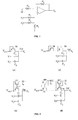
- Figure 1 shows the conventional way to implement a linear combiner and obtain at the output a weighted addition of two input voltages, by means of an operational amplifier and passive resistors.
- FIGS. 2(a), 2(b), 2(c) and 2(d) show different possible embodiments of the linear combiner of the invention:
- the component with a very high resistive value is implemented by means of a transistor 10 working in cut-off in diode connection to a biasing dc voltage V BIAS .
- the component with a very high resistive value is implemented by means of a group of series transistors 10 in diode connection
- the component with a very high resistive value is implemented by means of a transistor 11 working in the sub-threshold region.
- the component with a very high resistive value is implemented by means of a group of transistors 11 connected in series, which transistors are working in the sub-threshold region.
- V o f j ⁇ ⁇ R big ⁇ C 1 1 + j ⁇ ⁇ R big ⁇ C 1 + C 2 ⁇ V 1 f + j ⁇ ⁇ R big ⁇ C 2 1 + j ⁇ ⁇ R big ⁇ C 1 + C 2 ⁇ V 2 f
- R big represents the equivalent resistance of the component with a very high resistive value. So the transistors implement an extremely high resistance that sets the DC input level to V BIAS .
- the DC voltage at said node is V BIAS and the AC voltage at that node is the result of filtering the input voltages with a first-order high-pass filter, with a cut-off frequency of 1 / [2 ⁇ R big (C 1 + C 2 )] .
- V 0 V BIAS + a 1 ⁇ V 1 - V 1 ⁇ DC + a 2 ⁇ V 2 - V 2 ⁇ DC
- a 1 C 1 C 1 + C 2
- a 2 C 2 C 1 + C 2
- the linear combiner of the present invention may be used, for instance, as part of a demodulator in a zero-IF receiver.
- the down-conversion from the input RF signal is done at the DC level, so the method for demodulation used is based on zero-crossing detection. It greatly simplifies gain control of the receiver due to the use of amplitude limiters, and it allows for simple digital detection without requiring multibit analogue to digital converters (ADC).
- ADC analogue to digital converters
- sub-signals i k (t)-q k (t) which are combinations of these signals for the demodulation.
- the number of sub-signals i k (t)-q k (t) needed in each case depends on the type of signal and the modulation scheme. In the present example, eight combinations of the signal will be generated, which implies a division of the instantaneous phase in sixteen sectors with eight axes This provides the phase resolution that can obtained, which is needed in order to demodulate the phase or frequency modulated signal, by detecting the zero crossing angle or phase. It is necessary that the received waveform crosses zero at least once or more per symbol.
- the set of signals that has to be generated is a linear combination of the input signals, by means of product and additions.
- linear combiner in this case is implemented by means of eight identical linear combiner circuits, a sample of which has already been described and shown in figures 2(a)-2(d) ; each linear combiner will preferably be further connected to a limiting amplifier portion consisting of a differential preamplifier 20 and a latched comparator 30 ( figure 3 ).
- Each combined voltage V G1 and V G2 is applied at the input of a differential preamplifier 20, the input transistors M 1 and M 2 of said preamplifier working as QFG transistor
- V G ⁇ 1 V BIAS + C 1 C 1 + C 2 ⁇ i t + C 2 C 1 + C 2 ⁇ q t
- V G ⁇ 2 V BIAS
- a latched comparator 30 has been added after the preamplifier, in order to act, in combination with the preamplifier, as an amplitude limiter for the differential signal at the input of the preamplifier.
- the values of the two capacitors C 1 and C 2 have to be chosen so as to comply with such combination.
- the analogue part of the demodulator involves the linear combiner, the output of which is connected to an amplitude limiter.
- Figure 4 shows a second preferred embodiment of a linear combiner plus amplitude limiter for differential input signals i + (t) - i - (t) and q + (t) - q - (t) .
- an autozeroing circuit can be included to remove the offset of the input differential pair.
- Differential pairs usually have an input offset, which should be removed to achieve more accuracy. This offset is conventionally removed using autozeroing techniques Such well-known techniques can be easily incorporated in the preamplifier of Figure 4 .
- linear combiner as described hereinbefore has been developed for a specific type of Demodulator Nevertheless, the linear combiner of the present invention can be applied to any type of demodulator or circuit which requires a linear combination of signals.
- the linear combiner of the invention is not only valid for two input signals, but it can be used to combine N input signals.
- Figure 5 shows how it is possible to generalise to N input signals, showing a linear combiner having N differential input signals V 1 + - V 1 - , V 2 + - V 2 - , ... V N + - V N - .
- the linear combiner circuit consists of capacitive dividers formed by N capacitors C 1 , C 2 ,... C N and a MOS transistor 10 in diode connection to V BIAS that acts as a resistor for biasing.
- Each combined voltage V G1 and V G2 is applied at the input of a differential preamplifier 20, the input transistors M 1 and M 2 of said preamplifier working as QFG transistors
- the power consumption of the resulting circuit can be in the order of some microwatts, in the linear combiner of the present invention there is no quiescent power consumption, or it is negligible, that is to say, about three or four orders of magnitude lower.
- the present invention relates to a linear combiner It is to be understood that the above disclosure is an exemplification of the principles of the invention and does not limit the invention to the illustrated embodiments.
Landscapes
- Engineering & Computer Science (AREA)
- Computer Networks & Wireless Communication (AREA)
- Signal Processing (AREA)
- Power Engineering (AREA)
- Digital Transmission Methods That Use Modulated Carrier Waves (AREA)
Abstract
The invention refers to a linear combiner for linearly combining at set of N input signals (i(t), q(t)), Vk +-Vk -), N≥2, wherein.
- said N input signals are connected by means of respective N capacitors (Ck) to a single quasi-floating node (Out, G1, G2);
- said single quasi-floating node is further connected to a dc biasing voltage (VBIAS) by means of a component with a very high resistive value (10, 11), such that the current through the quasi-floating node is negligible;
such that the signal at said quasi-floating node (V0, VG1, VG2) is a weighted combination of the input signals (V1, V2, i(t), q(t), Vk + -Vk -)
- said N input signals are connected by means of respective N capacitors (Ck) to a single quasi-floating node (Out, G1, G2);
- said single quasi-floating node is further connected to a dc biasing voltage (VBIAS) by means of a component with a very high resistive value (10, 11), such that the current through the quasi-floating node is negligible;
such that the signal at said quasi-floating node (V0, VG1, VG2) is a weighted combination of the input signals (V1, V2, i(t), q(t), Vk + -Vk -)
Description
- The present invention is related to the field of wireless telecommunication systems, in particular reception and demodulation of digital coded schemes
- Frequency Shift Keying (FSK) is a common type of modulation used to transmit information between transmitters and receivers. One example is the well known Bluetooth receiver that uses Gaussian FSK (GFSK). The information is modulated in the transmitter and in order to recover such information in the receiver, the signal has to be demodulated, that is, the digital information of the signal has to be extracted, by means of a demodulator.
- Zero-crossing demodulators usually have a first analogue part which involves a linear combiner that by linearly combining the in-phase and quadrature signals (I and Q) generates a set of different sub-signals ik(t) and qk(t) and also amplitude limiters; and a digital part which generates the output data stream and the symbol synchronization circuit. The number of sub-signals ik(t)-qk(t) needed depends on the type of signal and the demodulation scheme.
- The conventional way to implement a linear combiner and obtain the weighted addition of two input voltages, is by means of operational amplifiers and passive resistors, as shown for example in
figure 1 ("Handbook of operational amplifier applications", Texas Instruments Application Report, SBOA092A, October 2001). In the operational amplifier shown, it is well known that V 0=a 1 V 1+a 2 V 2, where:

- However, this implementation shown in
fig 1 has the following drawbacks: - An operational amplifier is required for each linear combination, which involves high power consumption.
- The driving stage is resistively loaded.
- The closed-loop operation of the operational amplifier limits speed
- An input DC offset may saturate the output.
- Another implementation can be found in US patent
US-3934204 , which describes an AM/AGC weighted diversity combiner utilizing the AGC and AM voltages from the AGC loops of a pair of receivers for generating an optimum weighting signal or combining ratio. - The invention refers to a linear combiner according to
claim 1. Preferred embodiments of the linear combiner are defined in the dependent claim. - The present invention provides a compact circuit for a linear combiner, which overcomes the drawbacks of prior-art linear combiners as described before, since dissipating devices (such as resistors) are not used and the input signals are capacitively coupled to a quasi-floating node which provides a linear combination of the input signals.
- A first aspect of the invention relates to a linear combiner for linearly combining a set of N input signals, N being a natural number N≥2, wherein:
- said N input signals are connected by means of respective N capacitors Ck to a single quasi-floating node, whereby the input resistance of the linear combiner is infinite and its static power consumption is null; and wherein
- said single quasi-floating node is further connected to a dc biasing voltage VBIAS by means of a component with a very high resistive value -in the order of gigaohms-i.e., the resistive value of said component is sufficiently high so that the current through the quasi-floating node is negligible;
- With the linear combiner of the present invention, a linear combination of several input signals is achieved by means of capacitive division with an independent control of the dc level.
- Saturation by input offsets of the linear combiner is avoided since any de offset at the input(s) is not transmitted to the output. It is important e.g. in Zero-IF receivers as the signal is demodulated at baseband frequencies, which makes DC offsets one of the main problems in this kind of receivers.
- The component with a very high resistive value is preferably implemented by means of one or more transistors, such that the resulting design is efficient in terms of silicon area.
- Such one or more transistors can be worked in the cut-off mode, in diode connection; in this region the current going through such transistor is only the leakage current, and the equivalent resistance is very high Or it is also possible to have one or more transistors working in the subthreshold region This latter preferred embodiment provides a better precision when the DC voltage in the single node is established.
- In either case, if there is more than one transistor, they are preferably connected in series, such that the total resistance value is higher
- The quasi-floating node of the linear combiner is preferably connected to an amplifying stage, which amplifying stage is implemented by means of two transistors both working as Quasi-Floating Gate (QFG) transistors. Further, the amplifying stage preferably drives a latched comparator to achieve amplitude limitation of the input signals.
- In such case, the gate voltages VG1, VG2 of the two QFG transistors are:


- The amplifying stage can be any of a preamplifier, an operational amplifier or a differential amplifier.
- Advantages of the proposed linear combiner are the following:
- Linear combination of the inputs is carried out with zero quiescent power consumption.
- Comparator inputs can have rail-to-rail swing by properly choosing VBIAS, C1, C2-CN.
- The comparator is insensitive to the offset of inputs signals, since the dc level at the input of the preamplifier is set to VBIAS regardless of the input signals.
- A further aspect of the invention relates to a demodulator for detecting frequency-modulated signals, wherein said signals comprise an in-phase component (i(t)) and a quadrature component (q(t)), the demodulator comprises:
- a set of N1 linear combiners as defined herein-before, for generating a plurality of N1/2 in-phase signals (ik(t)) and a plurality of N1/2 quadrature signals (qk(t)), where 0≤k≤N1/2-1.
- The demodulator may further comprise:
- a plurality of N1 amplitude limiters, each of them being placed at the output of each of said N1 linear combiners, for providing a digital code associated to the respective in-phase (ik(t)) or quadrature (qk(t)) signal at the output of which they are placed, wherein said digital code represents the phase quantization sector of said in-phase (ik(t)) and quadrature (qk(t)) signals;
- decoding means providing a decoded symbol having log2(2N1) bits, each of said log2(2N1) bits being outputted in parallel;
- a set of log2(2N1) flip-flops, each of them being placed at the output of each of the log2(2N1) outputted bits, for delaying said log2(2N1)-bit symbol previously outputted;
- comparison means for comparing said log2(2N1) decoded symbol to said delayed log2(2N1)-bit decoded symbol to detect direction of the phase shift and thus to detect the data signal
- The demodulator may be part of a zero-IF receiver.
- To complete the description and in order to provide for a better understanding of the invention, a set of drawings is provided. Said drawings form an integral part of the description and illustrate preferred embodiments of the invention, which should not be interpreted as restricting the scope of the invention, but just as examples of how the invention can be embodied. The drawings comprise the following figures:
-
Figure 1 shows a conventional linear combiner. -
Figures 2(a), 2(b), 2(c) and 2(d) show several possible implementations of the linear combiner of the present invention. -
Figure 3 shows a first preferred embodiment of a linear combiner plus amplitude limiter for two single-ended input signals according to the invention. -
Figure 4 shows a second preferred embodiment of a linear combiner plus amplitude limiter for two differential inputs according to the invention. -
Figure 5 shows a further embodiment of a linear combiner plus amplitude limiter according to the invention, having N input signals. - Reference will now be made in detail to a preferred embodiment of the method of the present invention.
- As indicated before,
Figure 1 shows the conventional way to implement a linear combiner and obtain at the output a weighted addition of two input voltages, by means of an operational amplifier and passive resistors. -
Figures 2(a), 2(b), 2(c) and 2(d) show different possible embodiments of the linear combiner of the invention: - In
Figure 2(a) the component with a very high resistive value is implemented by means of atransistor 10 working in cut-off in diode connection to a biasing dc voltage VBIAS. And inFigure 2(b) the component with a very high resistive value is implemented by means of a group ofseries transistors 10 in diode connection - In
Figure 2(c) the component with a very high resistive value is implemented by means of atransistor 11 working in the sub-threshold region. And inFigure 2(b) the component with a very high resistive value is implemented by means of a group oftransistors 11 connected in series, which transistors are working in the sub-threshold region. - In the implementation shown in
figures 2(c) and 2(d) , when the transistor is working in the sub-threshold region, it is important that the current through the transistor is almost negligible, so that the corresponding equivalent resistance be very high (in the order of gigaohms). In order to do so, as shown in bothfigures 2(c) and 2(d) , a further transistor 11' may be used, connected as a current mirror, such that the current through the transistor(s) 11 is controlled by means of the current IB, and therefore it can be made as low as desired. An additional advantage of this lay-out is that the value of the equivalent resistance can also be controlled by means of varying IB. - In any of the embodiments shown in
figures 2(a)-2(d) , the signal added to VBIAS at the single common quasi-floating node is:
- In view of the high value of Rbig , the cutoff frequency of that high-pass filter is very low (less than 1 Hz), whereby the input signals lose their DC level, but they keep their AC contents. Therefore, the voltage at that node (at the output of the linear combiner) can be approximated to:


- The linear combiner of the present invention may be used, for instance, as part of a demodulator in a zero-IF receiver.
- In this case of a zero-IF receiver, the down-conversion from the input RF signal is done at the DC level, so the method for demodulation used is based on zero-crossing detection. It greatly simplifies gain control of the receiver due to the use of amplitude limiters, and it allows for simple digital detection without requiring multibit analogue to digital converters (ADC).
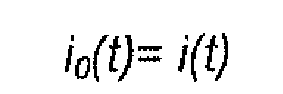
- Provided two quadrature signals at the receiver i(t) and q(t) (in-phase and quadrature, respectively), it is necessary to generate a set of sub-signals ik(t)-qk(t) which are combinations of these signals for the demodulation. The number of sub-signals ik(t)-qk(t) needed in each case depends on the type of signal and the modulation scheme. In the present example, eight combinations of the signal will be generated, which implies a division of the instantaneous phase in sixteen sectors with eight axes This provides the phase resolution that can obtained, which is needed in order to demodulate the phase or frequency modulated signal, by detecting the zero crossing angle or phase. It is necessary that the received waveform crosses zero at least once or more per symbol.
- According to the demodulator requirements assumed in the present example, such signal combination is the following:


- The set of signals that has to be generated is a linear combination of the input signals, by means of product and additions.
- To simplify the circuit, note that for the linear combinations to be implemented:


- As amplitude hard-limitation is employed after the linear combiner, the scaling factors multiplying the linear combinations of ik(t) and qk(t) need not be implemented, so the final expressions may be:





- So finally the first set of expressions [1] for the sub-signals ik(t) and qk(t), which would require twelve multiplications and six adding circuits, is simplified to the latter set [2] of simplified expressions, which requires just only four multipliers.
- The linear combiner in this case is implemented by means of eight identical linear combiner circuits, a sample of which has already been described and shown in
figures 2(a)-2(d) ; each linear combiner will preferably be further connected to a limiting amplifier portion consisting of adifferential preamplifier 20 and a latched comparator 30 (figure 3 ). - Each combined voltage VG1 and VG2 is applied at the input of a
differential preamplifier 20, the input transistors M1 and M2 of said preamplifier working as QFG transistor - The gate voltages of the QFG transistors M1 and M2 are:

- Hence by properly choosing C1 and C2 the weighting factors required are implemented.
- A latched
comparator 30 has been added after the preamplifier, in order to act, in combination with the preamplifier, as an amplitude limiter for the differential signal at the input of the preamplifier. - The output of the latched comparator is a square signal where zero crossings occur when VG1=VG2, i.e., when:

- Let's consider the following example, where one of the signal combinations to be obtained as required by the demodulator is the following:

- The values of the two capacitors C1 and C2 have to be chosen so as to comply with such combination.
- As indicated before, the analogue part of the demodulator involves the linear combiner, the output of which is connected to an amplitude limiter. Thus, the total amplitude of the signal is not important and the previous equation can be adjusted to the following:

- Then, it is necessary to chose C1 and C2 such that C1/(C1+C2)=1/1.4 and C2/(C1+C2)= 0.4/1.4. Thus, the chosen values are C2=0.4C1.
- It is thus an important factor that an embodiment of the linear combiner of the invention is used, thus capacitively coupling the input voltages to the floating gate of said QFG transistors.
-
Figure 4 shows a second preferred embodiment of a linear combiner plus amplitude limiter for differential input signals i + (t)-i - (t) and q + (t)-q - (t). - In this case, an autozeroing circuit can be included to remove the offset of the input differential pair. Differential pairs usually have an input offset, which should be removed to achieve more accuracy. This offset is conventionally removed using autozeroing techniques Such well-known techniques can be easily incorporated in the preamplifier of
Figure 4 . - The linear combiner as described hereinbefore has been developed for a specific type of Demodulator Nevertheless, the linear combiner of the present invention can be applied to any type of demodulator or circuit which requires a linear combination of signals.
- That is, the linear combiner of the invention is not only valid for two input signals, but it can be used to combine N input signals.
Figure 5 shows how it is possible to generalise to N input signals, showing a linear combiner having N differential input signals V1 +- V1 -, V2 +- V2 -, ... VN +- VN -. - The linear combiner circuit consists of capacitive dividers formed by N capacitors C1, C2,... CN and a
MOS transistor 10 in diode connection to VBIAS that acts as a resistor for biasing. - Each combined voltage VG1 and VG2 is applied at the input of a
differential preamplifier 20, the input transistors M1 and M2 of said preamplifier working as QFG transistors - The gate voltages of the QFG transistors M1 and M2 in this case are as follows:


- It is worth mentioning that while using standard techniques with resistances and operational amplifiers, the power consumption of the resulting circuit can be in the order of some microwatts, in the linear combiner of the present invention there is no quiescent power consumption, or it is negligible, that is to say, about three or four orders of magnitude lower.
- As indicated before, the present invention relates to a linear combiner It is to be understood that the above disclosure is an exemplification of the principles of the invention and does not limit the invention to the illustrated embodiments.
Claims (9)
- Linear combiner for linearly combining at set of N input signals (i(t), q(t), Vk +-Vk -), N≥2, wherein:- said N input signals are connected by means of respective N capacitors (Ck) to a single quasi-floating node (Out, G1, G2);- said single quasi-floating node is further connected to a dc biasing voltage (VBIAS) by means of a component with a resistive value (10, 11) being the resistive value sufficiently high such that the current through the quasi-floating node is negligible;the signal at said quasi-floating node (V0, VG1, VG2) being a weighted combination of the input signals (V1, V2, i(t), q(t), Vk +-Vk -).
- Linear combiner according to claim 1, wherein the element with a very-high resistive value is implemented by means of a transistor or a group of transistors in diode connection, in the case of a group of transistors they are connected in series.
- Linear combiner according to claim 1, wherein the element with a very-high resistive value is implemented by means of a transistor working in the subthreshold region or by means of a group of transistors working in the subthreshold region, when a group of transistors they are in series connection
- Demodulator for detecting frequency-modulated signals, wherein said signals comprise an in-phase component (i(t)) and a quadrature component (q(t)), the modulator comprises:- a set of N1 linear combiners according to any preceding claim, for generating a plurality of N1/2 in-phase signals (ik(t)) and a plurality of N1/2 quadrature signals (qk(t)), where 0≤k≤N1/2-1.
- Demodulator according to claim 4, wherein each quasi-floating node of the N1 linear combiners is connected to an amplifying stage (20), which each amplifying stage is implemented by means of two transistors (M1, M2) both working as QFG transistors.
- Demodulator according to claim 5, wherein in each of the N1 amplifying stages the gate voltages (VG1, VG2) of the QFG transistors M1 and M2 are:


- Demodulator according to any of claims 5-6, wherein each amplifying stage is connected to a latched comparator (30) in order to achieve amplitude limitation of the input signals.
- Demodulator according to claim 4, further comprising:- a plurality of N1 amplitude limiters, each of them being placed at the output of each of said N1 linear combiners, for providing a digital code associated to the respective in-phase (ik(t)) or quadrature (qk(t)) signal at the output of which they are placed, wherein said digital code represents the phase quantization sector of said in-phase (ik(t)) and quadrature (qk(t)) signals;- decoding means providing a decoded symbol having log2(2N1) bits, each of said log2(2N1) bits being outputted in parallel;- a set of log2(2N1) flip-flops, each of them being placed at the output of each of the log2(2N1) outputted bits, for delaying said log2(2N1)-bit symbol previously outputted;- comparison means for comparing said log2(2N1)-bit decoded symbol to said delayed log2(N1)-bit decoded symbol to detect direction of the phase shift and thus to detect the data signal.
- Demodulator according to any of claims 4-8, wherein said demodulator is part of a zero-IF receiver.
Priority Applications (1)
| Application Number | Priority Date | Filing Date | Title |
|---|---|---|---|
| EP08102494A EP2101456A1 (en) | 2008-03-11 | 2008-03-11 | Linear combiner |
Applications Claiming Priority (1)
| Application Number | Priority Date | Filing Date | Title |
|---|---|---|---|
| EP08102494A EP2101456A1 (en) | 2008-03-11 | 2008-03-11 | Linear combiner |
Publications (1)
| Publication Number | Publication Date |
|---|---|
| EP2101456A1 true EP2101456A1 (en) | 2009-09-16 |
Family
ID=40139252
Family Applications (1)
| Application Number | Title | Priority Date | Filing Date |
|---|---|---|---|
| EP08102494A Withdrawn EP2101456A1 (en) | 2008-03-11 | 2008-03-11 | Linear combiner |
Country Status (1)
| Country | Link |
|---|---|
| EP (1) | EP2101456A1 (en) |
Citations (2)
| Publication number | Priority date | Publication date | Assignee | Title |
|---|---|---|---|---|
| US3934204A (en) | 1974-10-04 | 1976-01-20 | The United States Of America As Represented By The Secretary Of The Navy | AM/AGC weighted diversity combiner/selector |
| WO2004040658A1 (en) * | 2002-10-30 | 2004-05-13 | Toumaz Technology Limited | Floating gate transistors |
-
2008
- 2008-03-11 EP EP08102494A patent/EP2101456A1/en not_active Withdrawn
Patent Citations (2)
| Publication number | Priority date | Publication date | Assignee | Title |
|---|---|---|---|---|
| US3934204A (en) | 1974-10-04 | 1976-01-20 | The United States Of America As Represented By The Secretary Of The Navy | AM/AGC weighted diversity combiner/selector |
| WO2004040658A1 (en) * | 2002-10-30 | 2004-05-13 | Toumaz Technology Limited | Floating gate transistors |
Non-Patent Citations (5)
| Title |
|---|
| "Texas Instruments Application Report", October 2001, article "Handbook of operational amplifier applications" |
| CARVAJAL R G ET AL: "Very Low-Voltage Analog Signal Processing Based on Quasi-Floating Gate Transistors", IEEE JOURNAL OF SOLID-STATE CIRCUITS, vol. 39, no. 3, 1 March 2004 (2004-03-01), IEEE SERVICE CENTER, PISCATAWAY, NJ, US, pages 434 - 442, XP011108372, ISSN: 0018-9200 * |
| GONZALEZ-CARVAJAL R ET AL: "A new family of very low-voltage analog circuits based on quasi-floating-gate transistors", IEEE TRANSACTIONS ON CIRCUITS AND SYSTEMS, vol. 50, no. 5, 1 May 2003 (2003-05-01), IEEE SERVICE CENTER, NEW YORK, NY, US, pages 214 - 220, XP011096141, ISSN: 1057-7130 * |
| NASS O ET AL: "Low-voltage pseudo floating-gate reconfigurable linear threshold elements", IEEE INTERNATIONAL JOINT CONFERENCE ON NEURAL NETWORKS, vol. 2, 31 July 2005 (2005-07-31), PISCATAWAY, NJ, USA,IEEE, US, pages 675 - 680, XP010866038, ISBN: 978-0-7803-9048-5 * |
| SAMADIAN S ET AL: "DEMODULATORS FOR A ZERO-IF BLUETOOTH RECEIVER", IEEE JOURNAL OF SOLID-STATE CIRCUITS, vol. 38, no. 8, 1 August 2003 (2003-08-01), IEEE SERVICE CENTER, PISCATAWAY, NJ, US, pages 1393 - 1396, XP001170979, ISSN: 0018-9200 * |
Similar Documents
| Publication | Publication Date | Title |
|---|---|---|
| WO2009030938A2 (en) | Multiplier, mixer, modulator, receiver and transmitter | |
| US6539066B1 (en) | Integrable radio receiver circuit for frequency-modulated digital signals | |
| TWI463848B (en) | Receiver and integrated am-fm/iq demodulators for gigabit-rate data detection | |
| EP1923991A2 (en) | Transmitter arrangement and signal processing method | |
| CN1124554A (en) | In-phase/quadrature phase quadrature modulation circuit | |
| EP1450289A1 (en) | Analog Divider Circuit and Method | |
| EP1289125A2 (en) | Double balance mixer circuit and orthogonal demodulation circuit using the same | |
| JPH088987A (en) | Phase detector | |
| US5309113A (en) | FSK data demodulator | |
| US6094571A (en) | Differential class AB mixer circuit | |
| US5436931A (en) | FSK receiver | |
| US8629716B2 (en) | Modulator, demodulator and modulator-demodulator | |
| US7907921B2 (en) | Wireless transmitter having multiple power amplifier drivers (PADs) that are selectively biased to provide substantially linear magnitude and phase responses | |
| EP2101456A1 (en) | Linear combiner | |
| US7664201B2 (en) | Digital automatic gain control | |
| JP2964573B2 (en) | Costas loop carrier recovery circuit | |
| US7271647B2 (en) | Active polyphase filter | |
| JP2748536B2 (en) | Quadrature signal demodulator | |
| US7107036B1 (en) | Demodulator architecture and associated methods | |
| US10432439B2 (en) | MSK transceiver of OQPSK data | |
| US4485359A (en) | Amplitude modulator having substantially zero modulation distortion | |
| US20040190654A1 (en) | Receiving apparatus | |
| US4403194A (en) | Closed loop amplitude demodulator | |
| JP3373960B2 (en) | Direct conversion receiver | |
| US4952887A (en) | Phase-lock loop circuit having outputs in quadrature |
Legal Events
| Date | Code | Title | Description |
|---|---|---|---|
| PUAI | Public reference made under article 153(3) epc to a published international application that has entered the european phase |
Free format text: ORIGINAL CODE: 0009012 |
|
| AK | Designated contracting states |
Kind code of ref document: A1 Designated state(s): AT BE BG CH CY CZ DE DK EE ES FI FR GB GR HR HU IE IS IT LI LT LU LV MC MT NL NO PL PT RO SE SI SK TR |
|
| AX | Request for extension of the european patent |
Extension state: AL BA MK RS |
|
| AKX | Designation fees paid | ||
| REG | Reference to a national code |
Ref country code: DE Ref legal event code: 8566 |
|
| STAA | Information on the status of an ep patent application or granted ep patent |
Free format text: STATUS: THE APPLICATION IS DEEMED TO BE WITHDRAWN |
|
| 18D | Application deemed to be withdrawn |
Effective date: 20100317 |