EP2101424A1 - Procédé et dispositif destinés à la transmission optique de données - Google Patents
Procédé et dispositif destinés à la transmission optique de données Download PDFInfo
- Publication number
- EP2101424A1 EP2101424A1 EP08015569A EP08015569A EP2101424A1 EP 2101424 A1 EP2101424 A1 EP 2101424A1 EP 08015569 A EP08015569 A EP 08015569A EP 08015569 A EP08015569 A EP 08015569A EP 2101424 A1 EP2101424 A1 EP 2101424A1
- Authority
- EP
- European Patent Office
- Prior art keywords
- light
- data
- emitting diode
- signal
- pulse width
- Prior art date
- Legal status (The legal status is an assumption and is not a legal conclusion. Google has not performed a legal analysis and makes no representation as to the accuracy of the status listed.)
- Granted
Links
- 238000000034 method Methods 0.000 title claims abstract description 48
- 230000005540 biological transmission Effects 0.000 claims abstract description 45
- 230000003287 optical effect Effects 0.000 claims abstract description 25
- 230000004044 response Effects 0.000 claims description 18
- 101100112084 Arabidopsis thaliana CRT2 gene Proteins 0.000 claims description 9
- 101100235014 Capsicum annuum LCY1 gene Proteins 0.000 claims description 9
- 230000004913 activation Effects 0.000 claims 1
- 230000006870 function Effects 0.000 description 11
- 238000012544 monitoring process Methods 0.000 description 8
- 230000008901 benefit Effects 0.000 description 5
- 238000010586 diagram Methods 0.000 description 4
- 238000012546 transfer Methods 0.000 description 3
- 238000004891 communication Methods 0.000 description 2
- 230000007423 decrease Effects 0.000 description 2
- 238000005286 illumination Methods 0.000 description 2
- 230000008569 process Effects 0.000 description 2
- 230000001953 sensory effect Effects 0.000 description 2
- 241000925028 Nitzschia sigma Species 0.000 description 1
- 230000002411 adverse Effects 0.000 description 1
- 238000013459 approach Methods 0.000 description 1
- 230000008859 change Effects 0.000 description 1
- 230000006735 deficit Effects 0.000 description 1
- 230000009977 dual effect Effects 0.000 description 1
- 230000000694 effects Effects 0.000 description 1
- 238000005265 energy consumption Methods 0.000 description 1
- 230000035755 proliferation Effects 0.000 description 1
- 230000005855 radiation Effects 0.000 description 1
Images


Classifications
-
- H—ELECTRICITY
- H04—ELECTRIC COMMUNICATION TECHNIQUE
- H04L—TRANSMISSION OF DIGITAL INFORMATION, e.g. TELEGRAPHIC COMMUNICATION
- H04L25/00—Baseband systems
- H04L25/38—Synchronous or start-stop systems, e.g. for Baudot code
- H04L25/40—Transmitting circuits; Receiving circuits
- H04L25/49—Transmitting circuits; Receiving circuits using code conversion at the transmitter; using predistortion; using insertion of idle bits for obtaining a desired frequency spectrum; using three or more amplitude levels ; Baseband coding techniques specific to data transmission systems
- H04L25/4902—Pulse width modulation; Pulse position modulation
-
- G—PHYSICS
- G08—SIGNALLING
- G08C—TRANSMISSION SYSTEMS FOR MEASURED VALUES, CONTROL OR SIMILAR SIGNALS
- G08C23/00—Non-electrical signal transmission systems, e.g. optical systems
- G08C23/04—Non-electrical signal transmission systems, e.g. optical systems using light waves, e.g. infrared
-
- H—ELECTRICITY
- H04—ELECTRIC COMMUNICATION TECHNIQUE
- H04B—TRANSMISSION
- H04B10/00—Transmission systems employing electromagnetic waves other than radio-waves, e.g. infrared, visible or ultraviolet light, or employing corpuscular radiation, e.g. quantum communication
- H04B10/11—Arrangements specific to free-space transmission, i.e. transmission through air or vacuum
- H04B10/114—Indoor or close-range type systems
- H04B10/1149—Arrangements for indoor wireless networking of information
Definitions
- the invention relates to a method and a device for the optical transmission of data by means of a pulse width modulated light emitting diode.
- LED light emitting diodes
- Light-emitting diodes are characterized by low energy consumption, a relatively long service life and good scalability.
- the data is transmitted in data packets. This allows secure data transmission by means of various data transmission protocols.
- the switching states of the light-emitting diode are sensed by a light sensor.
- the data is modulated by a modulation device to a pulse width modulated carrier signal.
- the pulse width modulated carrier signal is generated by a pulse width modulator from a voltage supply signal in response to an adjustable dimming control signal.
- At least one of the expected next turn-on phases of the light-emitting diode is determined as a function of detected switching times of the pulse-width-modulated carrier signal.
- This embodiment has the advantage that no light sensor for determining the switching states must be provided.
- the data is modulated by a modulation device to a voltage supply signal in response to a sensor signal of a light sensor.
- the data signal modulated onto the voltage supply signal is pulse-width modulated by a pulse width modulator as a function of an adjustable dimming control signal.
- At least one of the expected next turn-on phases of the light-emitting diode is determined as a function of the sensor-sensed switching times of the light signal emitted by the light-emitting diode.
- the data packets to be transmitted are buffered in at least one queue or data packet queue.
- a buffered data packet is deleted from the associated data packet queue only after error-free transmission.
- the data is transmitted optically via a wireless interface.
- the data is modulated by switching the pulse-width-modulated light-emitting diode on and off to the emitted light signal.
- the data can be modulated in a simple manner with low circuit complexity and high data transmission rate.
- the Anschaltphasenars sharks shark determines the turn-on of the light emitting diode in response to detected switching times of a pulse width modulated carrier signal, which is generated by a pulse width modulator from a power supply signal in response to an adjustable dimming control signal.
- the Anschaltphasenars sharks shark determines the turn-on of the light emitting diode in response to sensory detected switching times of the light emitted from the light emitting diode.
- the device 1 for the optical transmission of data by means of a pulse width modulated light-emitting diode 2 a Anschaltphasenars worn 3 and a modulation device 4.
- the device 1 receives via at least one signal line 6 data to be transmitted to the device 5.
- the light-emitting diode 2 emits a light signal, which is transmitted wirelessly to the further device 5.
- the device 5 is, for example, a portable device such as a mobile phone, a laptop or a PDA.
- the data to be transmitted comes from one or more data sources, which transmit the data directly or via a data network to the device 1.
- the data is preferably transmitted in data packets, wherein the data format of the data packets may be different.
- the data packets are, for example, Ethernet data packets or ATM data packets.
- the device 1 receives at least one data stream, which may consist of data packets. These data packets are cached in a possible embodiment in FIFO buffer as a data packet queue or in a queue.
- the device 1 for optical transmission of data is supplied with a supply voltage U s .
- the device 1 receives a dimming control signal CRTL Dimming for dimming the light emitting diode 2.
- the dimming control signal the light intensity of the light emitting diode 2 is set to illuminate the environment.
- the Anschaltphasenars worn 3 determines at least one expected turn-on of the light emitting diode 2 in response to a sequence of detected switching states of the light emitting diode 2.
- the modulation means 4 is provided for modulating data on the light emitted from the light emitting diode 2 light signal. In this case, the data is modulated onto the emitted light signal during the switching-on phases of the light-emitting diode 2 determined by the connection phase determination device 3.
- the Anschaltphasenarts prepared 3 receives a monitoring signal U m .
- the Anschaltphasenarts prepared 3 determined in one embodiment, one or more turn-on of the light emitting diode 2 as a function of detected switching times of a pulse-width-modulated carrier signal which is generated by the pulse width modulator from the voltage supply signal U s as a function of the adjustable dimming control signal CRTL Dimm .
- Fig. 2 shows a first embodiment of an inventive device 1 for the optical transmission of data by means of a pulse width modulated LED 2.
- the device 1 includes in the embodiment of Fig. 2 a pulse width modulator 6, which generates a pulse width modulated carrier signal.
- the pulse width modulator 6 receives a voltage supply signal U s and generates a pulse width modulated carrier signal in response to a dimming control signal CRTL dimming .
- the power supply signal is used to generate the pulse width modulated carrier signal.
- the control signal CRTL dimming sets the ratio between a phase in which the pulse width modulated signal has a logic high signal level, and a phase in which the pulse width modulated signal has a logic low signal level.
- expected switch-on phases of the light-emitting diode 2 are determined as a function of detected switching times of the pulse-width-modulated carrier signal delivered by the pulse width modulator 6.
- the pulse width modulated carrier signal is used in the in Fig. 2 illustrated embodiment as a monitoring signal U m .
- the device 1 contains a modulation device 7 for modulating the data onto a light signal emitted by the light-emitting diode 2 during the detected turn-on phases of the light-emitting diode 2 Fig. 2 1, the device 1 receives a WODT (wireless optical data transmission) modulator 7 of a large modulation bandwidth of, for example, up to 20 MHz.
- the light radiation emitted by the light-emitting diode 2 is varied to change the drive current I LED for the light-emitting diode 2.
- the WODT modulator 7 modulates the data onto the light signal emitted by the light-emitting diode 2 during the determined switch-on phases of the light-emitting diode 2 in accordance with the monitoring signal U m .
- the WODT modulator 7 receives the data to be modulated via one or more signal lines from corresponding data sources, preferably in packets.
- the data are preferably modulated by switching the pulse-width-modulated LED 2 within the determined turn-on phases of the light-emitting diode 2 on and off.
- Fig. 3 shows an alternative embodiment of the device 1 according to the invention for the optical transmission of data by means of a pulse width modulated light emitting diode 2. The device 1 is obtained in the in Fig.
- the pulse width modulator 6 is connected downstream of the WODT modulator 7.
- the device 1 at the in Fig. 3 illustrated embodiment a sensor 8, the sensor 2, the switching states of the light emitting diode detected.
- the sensor 8 is, for example, a photodetector.
- the data is modulated by the WODT modulator 7 on the voltage supply signal U s in response to a sensor signal U m of the light sensor 8. Subsequently, the modulated by the voltage supply signal U s data signal is pulse width modulated by the pulse width modulator 6 in response to an adjustable dimming control signal CRTL dimming .
- the sensor 8 may be any desired light sensor, for example a photodiode.
- the pulse width modulator 6 and the light-emitting diode 2 form an integrated component.
- the WODT modulator 7 with the light emitting diode 2 form an integrated component.
- Fig. 4 shows a simple flowchart of the method according to the invention for the optical transmission of data by means of a pulse width modulated LED 2.
- future switching-on phases of the light emitting diode 2 are determined in a step S1 in response to a sequence of detected switching states of the light emitting diode 2.
- These switching states are switching states of the light emitting diode 2, which has taken these in the past.
- at least one of the next or future expected switching-on phases of the light-emitting diode 2 is determined as a function of detected switching times of a pulse-width-modulated carrier signal.
- next expected switch-on phases of the light-emitting diode 2 are determined as a function of the sensor-sensed switching times of the light signal emitted by the light-emitting diode 2.
- the turn-on phases are calculated as a function of the switching times by means of a calculation device.
- the calculation device is, for example, a microprocessor.
- step S2 the data to be transmitted are then modulated onto a light signal emitted by the light-emitting diode 2 during the determined turn-on phases of the light-emitting diode 2.
- step S3 the method ends.
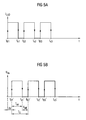
- FIGS. 5A and 5B show signal diagrams for explaining the procedure in the inventive method for transmitting data.
- Fig. 5A shows a drive current I LED for the LED 2.
- Fig. 5B shows the monitoring signal U m , which is used to determine future turn-on of the light emitting diode 2.
- a switch-on phase begins at a time T b and ends at a time T e .
- the beginning of the third switch-on phase of the light-emitting diode T b3 can be calculated from the monitoring signal U m as follows:
- T 0 t b ⁇ 2 ⁇ ' - t b ⁇ 1 ⁇ ' ,
- T ON t e ⁇ 1 ⁇ ' - t b ⁇ 1 ⁇ ' ,
- the next or third switch-on phase of the light-emitting diode 2 is thus determined from the sequence of detected switching states of the light-emitting diode 2, ie the monitoring signal which images the first and second switch-on phase of the light-emitting diode 2.
- the data to be transmitted are then modulated onto the light signal during this determined third switch-on phase of the light-emitting diode 2. If the time delay ⁇ t is completely known or unknown, but shorter than the duration of a data symbol, the WODT modulator 7 detects the start time t bj and the end time t ej for each portion of the PWM modulated signal, ie, the start and end times switched-on.
- M s is the symbol rate
- L i s the dual logarithm of the number of signal levels of a data symbol
- T on, j the duration of the switched-on phase of a time segment j, r j to the bit length of the data block or the data packet i
- M is the highest packet number of the during a PWM period of time j sending data packet and t empty.j represents the time in which the queue is empty between t bj and t ej .
- the data packet is transmitted, ie the data of the data packet are modulated onto the light signal emitted by the light-emitting diode 2 during the switch-on phase.
- the last transmitted data packet is held in the memory or the queue until it is determined that the transmission of the data packet is completely completed, ie that during the transmission of the data packet no power-off phase has occurred. This is necessary in particular because of the time delay ⁇ t between the optical output signal and the monitoring signal U m .
- the data packets whose data has been successfully transmitted to the mobile device 5 can then be deleted.
- the data packet queue is serviced until t ej is reached. Between the times t ej and t b, j + 1 , incoming data packets are sorted into the data packet queue and transmitted during the next power-up phase.
- the dimming of the light signal in response to the dimming control signal CRTL Dimm has the following effects on the data transmission. If the dimming factor ⁇ decreases, the duration of the switch-on phase T ON increases. Due to the increasing duration of the connection phase, the available time for transmitting data of the data packets increases, ie the data packet transmission is not adversely affected by the dimming process. On the other hand, if the dimming factor ⁇ increases, so that the duration of the switch-on phase T ON decreases, this can lead to a packet loss. However, if the next power-up phase is recognizable and the lost data packet is still available, ie the data packet queue is in stock, the data packet may fail possible embodiment during the next power-on phase to be retransmitted.
- n.gtoreq.1 is suitably selectable, by a high one Reliability to ensure that the start-up phase of the pulse width modulated signal has started at this time.
- t ej can be replaced by t ej -n • ⁇ and T onj with T onj - 2n • ⁇ .
- n is selected, the lower the probability that a data packet will be transmitted during a time in which the LED 2 is actually turned off.
- the number n may not be too large, otherwise the efficiency of the data transmission will be too low.
- the device 1 receives a feedback signal from the mobile terminal 5 or not.
- the device 1 receives a feedback signal via a separate message transmission channel as to whether a data packet has been completely transmitted or not.
- the data packets may be provided, for example, by a monotonously increasing frame or packet number.
- the receiver or mobile device 5 may request retransmission of a missing or erroneous data packet.
- the data transmission device 1 receives data packets from different data sources which are waiting for transmission in different data packet queues.
- the device 1 additionally comprises a so-called "scheduler" which manages the various data packet queues. This scheduler identifies which data packet queue between the time t bj and t ej to serve next. Then the scheduler checks whether or not there is a data packet in the selected data packet queue. If there is a data packet, the device 1 starts transmitting data packets from the corresponding queue. In this case, the last transmitted data packets are held in the memory until an error-free data packet transmission has taken place. Only those data packets whose data has been transmitted successfully to the mobile terminal 5 are deleted. The process is repeated until the time t ej is reached.
- j + 1 incoming data packets are sorted in the corresponding data packet queues and sent out during the next transmission period.
- the inventive method is not only suitable for the optical transmission of data within data packets, but also for the transmission of data of continuous data streams.
- the average optical power of the emitted light signal is kept constant during the modulation.
- a high data transmission rate can be achieved with simultaneous dimming of the light-emitting diode 2.
- bit rates or data transmission rates in the range of the transmission rate at reference power P 0 ie a dimming factor of 0%
- bit rates or data transmission rates in the range of the transmission rate at reference power P 0 can be achieved by a factor (1- ⁇ ).
- the data rate may approach 70% of the data rate achievable with 100% illumination.
- the data to be transmitted is data of any application, such as multimedia data, such as for audio applications.
- the inventive method for optical transmission of data does not cause electromagnetic waves and can not be affected by electromagnetic waves.
- the method according to the invention can be used in particular if an LED illumination is already provided.
- the LEDs can be addressed, for example, with Powerline.
- the transmission of the data takes place by means of an easily shieldable communication medium.
- the data is transmitted optically, it can be easily shielded with a wall or curtain. It can therefore be achieved a security against eavesdropping.
- the light signal emitted by the light-emitting diode 2 is aligned conically. This makes it possible to form a relatively small cell size, which enables individual and high-bit-rate communication.
- the inventive method allows the secure optical transmission of data via a dimmable LED 2 to portable terminals 5 within a lighted room and is insensitive to radio signals. Any light-emitting diodes 2 can be used, for example light-emitting diodes which generate a white light. Even light diodes with a smaller modulation bandwidth than white LEDs can be used.
Landscapes
- Engineering & Computer Science (AREA)
- Physics & Mathematics (AREA)
- Computer Networks & Wireless Communication (AREA)
- Signal Processing (AREA)
- Computing Systems (AREA)
- Electromagnetism (AREA)
- Spectroscopy & Molecular Physics (AREA)
- General Physics & Mathematics (AREA)
- Optical Communication System (AREA)
Priority Applications (5)
| Application Number | Priority Date | Filing Date | Title |
|---|---|---|---|
| EP08015569A EP2101424B1 (fr) | 2008-03-10 | 2008-09-03 | Procédé et dispositif destinés à la transmission optique de données |
| CN200980108571.4A CN101971529B (zh) | 2008-03-10 | 2009-02-25 | 用于光学传输数据的方法和装置 |
| US12/920,490 US8744273B2 (en) | 2008-03-10 | 2009-02-25 | Method and device for the optical transmission of data |
| PCT/EP2009/052223 WO2009112365A1 (fr) | 2008-03-10 | 2009-02-25 | Procédé et dispositif de transmission optique de données |
| KR1020107022553A KR101379812B1 (ko) | 2008-03-10 | 2009-02-25 | 데이터의 광학 전송을 위한 방법 및 장치 |
Applications Claiming Priority (2)
| Application Number | Priority Date | Filing Date | Title |
|---|---|---|---|
| EP08004419 | 2008-03-10 | ||
| EP08015569A EP2101424B1 (fr) | 2008-03-10 | 2008-09-03 | Procédé et dispositif destinés à la transmission optique de données |
Publications (2)
| Publication Number | Publication Date |
|---|---|
| EP2101424A1 true EP2101424A1 (fr) | 2009-09-16 |
| EP2101424B1 EP2101424B1 (fr) | 2013-02-27 |
Family
ID=40793227
Family Applications (1)
| Application Number | Title | Priority Date | Filing Date |
|---|---|---|---|
| EP08015569A Not-in-force EP2101424B1 (fr) | 2008-03-10 | 2008-09-03 | Procédé et dispositif destinés à la transmission optique de données |
Country Status (5)
| Country | Link |
|---|---|
| US (1) | US8744273B2 (fr) |
| EP (1) | EP2101424B1 (fr) |
| KR (1) | KR101379812B1 (fr) |
| CN (1) | CN101971529B (fr) |
| WO (1) | WO2009112365A1 (fr) |
Cited By (2)
| Publication number | Priority date | Publication date | Assignee | Title |
|---|---|---|---|---|
| EP2315187A3 (fr) * | 2009-10-06 | 2011-11-16 | Samsung Electronics Co., Ltd. | Appareil d'affichage, système et procédé de sortie de données |
| US9319134B2 (en) | 2009-04-28 | 2016-04-19 | Siemens Aktiengesellschaft | Method and device for optically transmitting data |
Families Citing this family (12)
| Publication number | Priority date | Publication date | Assignee | Title |
|---|---|---|---|---|
| EP2101424B1 (fr) | 2008-03-10 | 2013-02-27 | Siemens Aktiengesellschaft | Procédé et dispositif destinés à la transmission optique de données |
| US8873965B2 (en) * | 2012-04-10 | 2014-10-28 | Disney Enterprises, Inc. | Visible light communication with flickering prevention |
| CN105102996B (zh) | 2013-04-12 | 2018-01-02 | 爱德万测试公司 | 输入和输出路径的扫描速度优化 |
| US9264138B2 (en) | 2013-05-16 | 2016-02-16 | Disney Enterprises, Inc. | Reliable visibile light communication with dark light synchronization |
| DE102013009274A1 (de) * | 2013-06-04 | 2014-12-04 | Fresenius Medical Care Deutschland Gmbh | Optisches Übertragungsverfahren von Daten durch Modulation der Displayhintergrundbeleuchtung insbesondere bei medizintechnischen Geräten |
| US10009100B2 (en) | 2014-06-18 | 2018-06-26 | Qualcomm Incorporated | Transmission of identifiers using visible light communication |
| US9455787B2 (en) * | 2014-10-28 | 2016-09-27 | Cisco Technology, Inc. | Light emitting diode (LED)-based multi-bitrate data links |
| DE102015200214A1 (de) * | 2015-01-09 | 2016-07-14 | Siemens Healthcare Gmbh | Verfahren zur Kommunikation in einer Magnetresonanzeinrichtung und Magnetresonanzeinrichtung |
| GB201701209D0 (en) * | 2017-01-24 | 2017-03-08 | Purelifi Ltd | Optical wireless communication system |
| JP6622782B2 (ja) * | 2017-11-24 | 2019-12-18 | ファナック株式会社 | 制御装置、電子機器、及び制御システム |
| EP4147380A1 (fr) * | 2020-05-08 | 2023-03-15 | Signify Holding B.V. | Économie d'énergie pour un système de communication optique sans fil |
| KR102609128B1 (ko) * | 2022-02-11 | 2023-12-04 | (주)위드비어 | 아날로그 노이즈 저감을 위한 장거리 전송 시스템 |
Citations (4)
| Publication number | Priority date | Publication date | Assignee | Title |
|---|---|---|---|---|
| WO2002025842A2 (fr) * | 2000-09-19 | 2002-03-28 | Color Kinetics Incorporated | Procedes et systemes pour reseau d'eclairage universel |
| US20060239689A1 (en) * | 2005-01-25 | 2006-10-26 | Tir Systems, Ltd. | Method and apparatus for illumination and communication |
| WO2006123697A1 (fr) * | 2005-05-20 | 2006-11-23 | Nakagawa Laboratories, Inc. | Appareil d’émission de données et appareil de réception de données |
| US20070104075A1 (en) * | 2005-01-06 | 2007-05-10 | Inra-Com Ltd | Communication diode driver circuit |
Family Cites Families (6)
| Publication number | Priority date | Publication date | Assignee | Title |
|---|---|---|---|---|
| JP2007527170A (ja) * | 2004-02-19 | 2007-09-20 | ジョージア テック リサーチ コーポレイション | 並列通信のためのシステムおよび方法 |
| US20070273290A1 (en) * | 2004-11-29 | 2007-11-29 | Ian Ashdown | Integrated Modular Light Unit |
| US7570246B2 (en) * | 2005-08-01 | 2009-08-04 | Avago Technologies Ecbu Ip (Singapore) Pte. Ltd. | Method and apparatus for communication using pulse-width-modulated visible light |
| JP4725843B2 (ja) * | 2005-08-25 | 2011-07-13 | 横河電機株式会社 | 光パケットネットワークシステム |
| CN100521581C (zh) | 2007-07-13 | 2009-07-29 | 北京航空航天大学 | 保证服务质量的多址接入方法 |
| EP2101424B1 (fr) | 2008-03-10 | 2013-02-27 | Siemens Aktiengesellschaft | Procédé et dispositif destinés à la transmission optique de données |
-
2008
- 2008-09-03 EP EP08015569A patent/EP2101424B1/fr not_active Not-in-force
-
2009
- 2009-02-25 US US12/920,490 patent/US8744273B2/en not_active Expired - Fee Related
- 2009-02-25 WO PCT/EP2009/052223 patent/WO2009112365A1/fr active Application Filing
- 2009-02-25 KR KR1020107022553A patent/KR101379812B1/ko not_active IP Right Cessation
- 2009-02-25 CN CN200980108571.4A patent/CN101971529B/zh not_active Expired - Fee Related
Patent Citations (5)
| Publication number | Priority date | Publication date | Assignee | Title |
|---|---|---|---|---|
| WO2002025842A2 (fr) * | 2000-09-19 | 2002-03-28 | Color Kinetics Incorporated | Procedes et systemes pour reseau d'eclairage universel |
| US20070104075A1 (en) * | 2005-01-06 | 2007-05-10 | Inra-Com Ltd | Communication diode driver circuit |
| US20060239689A1 (en) * | 2005-01-25 | 2006-10-26 | Tir Systems, Ltd. | Method and apparatus for illumination and communication |
| WO2006123697A1 (fr) * | 2005-05-20 | 2006-11-23 | Nakagawa Laboratories, Inc. | Appareil d’émission de données et appareil de réception de données |
| EP1912354A1 (fr) * | 2005-05-20 | 2008-04-16 | Nakagawa Laboratories, Inc. | Appareil d émission de données et appareil de réception de données |
Cited By (2)
| Publication number | Priority date | Publication date | Assignee | Title |
|---|---|---|---|---|
| US9319134B2 (en) | 2009-04-28 | 2016-04-19 | Siemens Aktiengesellschaft | Method and device for optically transmitting data |
| EP2315187A3 (fr) * | 2009-10-06 | 2011-11-16 | Samsung Electronics Co., Ltd. | Appareil d'affichage, système et procédé de sortie de données |
Also Published As
| Publication number | Publication date |
|---|---|
| CN101971529A (zh) | 2011-02-09 |
| EP2101424B1 (fr) | 2013-02-27 |
| US8744273B2 (en) | 2014-06-03 |
| KR101379812B1 (ko) | 2014-04-01 |
| WO2009112365A1 (fr) | 2009-09-17 |
| KR20100139008A (ko) | 2010-12-31 |
| CN101971529B (zh) | 2015-09-23 |
| US20110052210A1 (en) | 2011-03-03 |
Similar Documents
| Publication | Publication Date | Title |
|---|---|---|
| EP2101424B1 (fr) | Procédé et dispositif destinés à la transmission optique de données | |
| DE102010005885A1 (de) | Verfahren und Vorrichtung zur optischen Übertragung von Daten | |
| EP2174432B1 (fr) | Système de transmission de données et procédé de transmission de données dans un système de transmission de données | |
| DE69627886T2 (de) | Robustes verfahren und vorrichtung zur leitungsgebundenen optischen mehrmodenübertragung | |
| DE69737494T2 (de) | Echtzeit-csma-verfahren welches die fähigkeit besitzt die zellgrösse adaptiv zu verändern und drahtloses netzwerk zur durchführung des verfahrens | |
| DE69411954T2 (de) | Drahtloses optisches übertragungssystem mit adaptiver datenübertragungsgeschwindigkeit | |
| EP2425558B1 (fr) | Procédé et dispositif de transfert optique de données | |
| EP1772040B1 (fr) | Circuit d'interface destine a la transmission de signaux numeriques | |
| EP2514127B1 (fr) | Procédé et dispositif de transmission optique de données | |
| WO2020120555A1 (fr) | Station d'abonnés pour un système de bus série et procédé de communication dans un système de bus série | |
| DE10043284C1 (de) | Funkgerät | |
| EP3556058A1 (fr) | Station d'abonné pour un système de bus et procédé de transmission de données dans un système de bus | |
| DE102007043255B4 (de) | Verfahren und Anordnung zur Aussendung von Daten | |
| MXPA05006678A (es) | Metodo y aparato para transmision de datos a traves de un enlace inverso en un sistema de comunicacion. | |
| EP1408630B1 (fr) | Procède de transmission d'un signal optique | |
| AT16154U1 (de) | Leuchtmittel-Konverter und Leuchtmittel-Modul mit Zweidraht-Kommunikation | |
| DE102007011176A1 (de) | Schaltungsanordnung eines optischen Senders, Schaltungsanordnung eines optischen Empfängers, optoelektronische Sende- und Empfangsanordnung mit derartigen Schaltungsanordnungen und Verfahren der optischen Datenübertragung | |
| CN102326431A (zh) | 通信设备和方法、以及包含这种设备的系统 | |
| DE102020200803A1 (de) | Sende-/Empfangseinrichtung und Kommunikationssteuereinrichtung für eine Teilnehmerstation eines seriellen Bussystems und Verfahren zur Kommunikation in einem seriellen Bussystem | |
| EP1128630A2 (fr) | Méthode de transmission d'informations vers un récepteur | |
| EP4029201A1 (fr) | Dispositif pour une station d'abonné d'un système de bus série et procédé de communication dans un système de bus série | |
| EP0847182A2 (fr) | Système d'interphone et régulateur de courant pour l'alimentation de celui-ci | |
| DE2620250A1 (de) | Sprechfunkgeraet mit einem sendeteil, der vorzugsweise eine kennung des geraetes symbolisierende datentelegramme periodisch aussenden kann | |
| DE19855225A1 (de) | Verfahren zum Einstellen einer Strahlungsleistung in einem Sender | |
| EP1791273A2 (fr) | Procédé et appareil pour éliminer le bruit dans un récepteur |
Legal Events
| Date | Code | Title | Description |
|---|---|---|---|
| PUAI | Public reference made under article 153(3) epc to a published international application that has entered the european phase |
Free format text: ORIGINAL CODE: 0009012 |
|
| AK | Designated contracting states |
Kind code of ref document: A1 Designated state(s): AT BE BG CH CY CZ DE DK EE ES FI FR GB GR HR HU IE IS IT LI LT LU LV MC MT NL NO PL PT RO SE SI SK TR |
|
| AX | Request for extension of the european patent |
Extension state: AL BA MK RS |
|
| 17P | Request for examination filed |
Effective date: 20100315 |
|
| 17Q | First examination report despatched |
Effective date: 20100409 |
|
| AKX | Designation fees paid |
Designated state(s): AT BE BG CH CY CZ DE DK EE ES FI FR GB GR HR HU IE IS IT LI LT LU LV MC MT NL NO PL PT RO SE SI SK TR |
|
| GRAP | Despatch of communication of intention to grant a patent |
Free format text: ORIGINAL CODE: EPIDOSNIGR1 |
|
| GRAS | Grant fee paid |
Free format text: ORIGINAL CODE: EPIDOSNIGR3 |
|
| REG | Reference to a national code |
Ref country code: DE Ref legal event code: R079 Ref document number: 502008009309 Country of ref document: DE Free format text: PREVIOUS MAIN CLASS: H04B0010100000 Ipc: H04B0010110000 |
|
| GRAA | (expected) grant |
Free format text: ORIGINAL CODE: 0009210 |
|
| AK | Designated contracting states |
Kind code of ref document: B1 Designated state(s): AT BE BG CH CY CZ DE DK EE ES FI FR GB GR HR HU IE IS IT LI LT LU LV MC MT NL NO PL PT RO SE SI SK TR |
|
| REG | Reference to a national code |
Ref country code: GB Ref legal event code: FG4D Free format text: NOT ENGLISH |
|
| RIC1 | Information provided on ipc code assigned before grant |
Ipc: H04L 25/49 20060101ALI20130122BHEP Ipc: G08C 23/04 20060101ALI20130122BHEP Ipc: H04B 10/11 20130101AFI20130122BHEP |
|
| REG | Reference to a national code |
Ref country code: CH Ref legal event code: EP |
|
| RAP2 | Party data changed (patent owner data changed or rights of a patent transferred) |
Owner name: SIEMENS AKTIENGESELLSCHAFT |
|
| REG | Reference to a national code |
Ref country code: AT Ref legal event code: REF Ref document number: 598953 Country of ref document: AT Kind code of ref document: T Effective date: 20130315 |
|
| REG | Reference to a national code |
Ref country code: IE Ref legal event code: FG4D Free format text: LANGUAGE OF EP DOCUMENT: GERMAN |
|
| REG | Reference to a national code |
Ref country code: DE Ref legal event code: R096 Ref document number: 502008009309 Country of ref document: DE Effective date: 20130418 |
|
| REG | Reference to a national code |
Ref country code: NL Ref legal event code: T3 |
|
| REG | Reference to a national code |
Ref country code: LT Ref legal event code: MG4D |
|
| PG25 | Lapsed in a contracting state [announced via postgrant information from national office to epo] |
Ref country code: IS Free format text: LAPSE BECAUSE OF FAILURE TO SUBMIT A TRANSLATION OF THE DESCRIPTION OR TO PAY THE FEE WITHIN THE PRESCRIBED TIME-LIMIT Effective date: 20130627 Ref country code: BG Free format text: LAPSE BECAUSE OF FAILURE TO SUBMIT A TRANSLATION OF THE DESCRIPTION OR TO PAY THE FEE WITHIN THE PRESCRIBED TIME-LIMIT Effective date: 20130527 Ref country code: NO Free format text: LAPSE BECAUSE OF FAILURE TO SUBMIT A TRANSLATION OF THE DESCRIPTION OR TO PAY THE FEE WITHIN THE PRESCRIBED TIME-LIMIT Effective date: 20130527 Ref country code: SE Free format text: LAPSE BECAUSE OF FAILURE TO SUBMIT A TRANSLATION OF THE DESCRIPTION OR TO PAY THE FEE WITHIN THE PRESCRIBED TIME-LIMIT Effective date: 20130227 Ref country code: ES Free format text: LAPSE BECAUSE OF FAILURE TO SUBMIT A TRANSLATION OF THE DESCRIPTION OR TO PAY THE FEE WITHIN THE PRESCRIBED TIME-LIMIT Effective date: 20130607 Ref country code: LT Free format text: LAPSE BECAUSE OF FAILURE TO SUBMIT A TRANSLATION OF THE DESCRIPTION OR TO PAY THE FEE WITHIN THE PRESCRIBED TIME-LIMIT Effective date: 20130227 |
|
| PG25 | Lapsed in a contracting state [announced via postgrant information from national office to epo] |
Ref country code: PL Free format text: LAPSE BECAUSE OF FAILURE TO SUBMIT A TRANSLATION OF THE DESCRIPTION OR TO PAY THE FEE WITHIN THE PRESCRIBED TIME-LIMIT Effective date: 20130227 Ref country code: GR Free format text: LAPSE BECAUSE OF FAILURE TO SUBMIT A TRANSLATION OF THE DESCRIPTION OR TO PAY THE FEE WITHIN THE PRESCRIBED TIME-LIMIT Effective date: 20130528 Ref country code: SI Free format text: LAPSE BECAUSE OF FAILURE TO SUBMIT A TRANSLATION OF THE DESCRIPTION OR TO PAY THE FEE WITHIN THE PRESCRIBED TIME-LIMIT Effective date: 20130227 Ref country code: PT Free format text: LAPSE BECAUSE OF FAILURE TO SUBMIT A TRANSLATION OF THE DESCRIPTION OR TO PAY THE FEE WITHIN THE PRESCRIBED TIME-LIMIT Effective date: 20130627 Ref country code: FI Free format text: LAPSE BECAUSE OF FAILURE TO SUBMIT A TRANSLATION OF THE DESCRIPTION OR TO PAY THE FEE WITHIN THE PRESCRIBED TIME-LIMIT Effective date: 20130227 Ref country code: LV Free format text: LAPSE BECAUSE OF FAILURE TO SUBMIT A TRANSLATION OF THE DESCRIPTION OR TO PAY THE FEE WITHIN THE PRESCRIBED TIME-LIMIT Effective date: 20130227 |
|
| PG25 | Lapsed in a contracting state [announced via postgrant information from national office to epo] |
Ref country code: HR Free format text: LAPSE BECAUSE OF FAILURE TO SUBMIT A TRANSLATION OF THE DESCRIPTION OR TO PAY THE FEE WITHIN THE PRESCRIBED TIME-LIMIT Effective date: 20130227 |
|
| PG25 | Lapsed in a contracting state [announced via postgrant information from national office to epo] |
Ref country code: SK Free format text: LAPSE BECAUSE OF FAILURE TO SUBMIT A TRANSLATION OF THE DESCRIPTION OR TO PAY THE FEE WITHIN THE PRESCRIBED TIME-LIMIT Effective date: 20130227 Ref country code: CZ Free format text: LAPSE BECAUSE OF FAILURE TO SUBMIT A TRANSLATION OF THE DESCRIPTION OR TO PAY THE FEE WITHIN THE PRESCRIBED TIME-LIMIT Effective date: 20130227 Ref country code: EE Free format text: LAPSE BECAUSE OF FAILURE TO SUBMIT A TRANSLATION OF THE DESCRIPTION OR TO PAY THE FEE WITHIN THE PRESCRIBED TIME-LIMIT Effective date: 20130227 Ref country code: RO Free format text: LAPSE BECAUSE OF FAILURE TO SUBMIT A TRANSLATION OF THE DESCRIPTION OR TO PAY THE FEE WITHIN THE PRESCRIBED TIME-LIMIT Effective date: 20130227 Ref country code: DK Free format text: LAPSE BECAUSE OF FAILURE TO SUBMIT A TRANSLATION OF THE DESCRIPTION OR TO PAY THE FEE WITHIN THE PRESCRIBED TIME-LIMIT Effective date: 20130227 |
|
| PG25 | Lapsed in a contracting state [announced via postgrant information from national office to epo] |
Ref country code: CY Free format text: LAPSE BECAUSE OF FAILURE TO SUBMIT A TRANSLATION OF THE DESCRIPTION OR TO PAY THE FEE WITHIN THE PRESCRIBED TIME-LIMIT Effective date: 20130227 |
|
| PG25 | Lapsed in a contracting state [announced via postgrant information from national office to epo] |
Ref country code: IT Free format text: LAPSE BECAUSE OF FAILURE TO SUBMIT A TRANSLATION OF THE DESCRIPTION OR TO PAY THE FEE WITHIN THE PRESCRIBED TIME-LIMIT Effective date: 20130227 |
|
| PLBE | No opposition filed within time limit |
Free format text: ORIGINAL CODE: 0009261 |
|
| STAA | Information on the status of an ep patent application or granted ep patent |
Free format text: STATUS: NO OPPOSITION FILED WITHIN TIME LIMIT |
|
| 26N | No opposition filed |
Effective date: 20131128 |
|
| REG | Reference to a national code |
Ref country code: DE Ref legal event code: R097 Ref document number: 502008009309 Country of ref document: DE Effective date: 20131128 |
|
| BERE | Be: lapsed |
Owner name: SIEMENS A.G. Effective date: 20130930 |
|
| PG25 | Lapsed in a contracting state [announced via postgrant information from national office to epo] |
Ref country code: MC Free format text: LAPSE BECAUSE OF FAILURE TO SUBMIT A TRANSLATION OF THE DESCRIPTION OR TO PAY THE FEE WITHIN THE PRESCRIBED TIME-LIMIT Effective date: 20130227 |
|
| REG | Reference to a national code |
Ref country code: CH Ref legal event code: PL |
|
| REG | Reference to a national code |
Ref country code: IE Ref legal event code: MM4A |
|
| PG25 | Lapsed in a contracting state [announced via postgrant information from national office to epo] |
Ref country code: LI Free format text: LAPSE BECAUSE OF NON-PAYMENT OF DUE FEES Effective date: 20130930 Ref country code: CH Free format text: LAPSE BECAUSE OF NON-PAYMENT OF DUE FEES Effective date: 20130930 Ref country code: BE Free format text: LAPSE BECAUSE OF NON-PAYMENT OF DUE FEES Effective date: 20130930 Ref country code: IE Free format text: LAPSE BECAUSE OF NON-PAYMENT OF DUE FEES Effective date: 20130903 |
|
| REG | Reference to a national code |
Ref country code: AT Ref legal event code: MM01 Ref document number: 598953 Country of ref document: AT Kind code of ref document: T Effective date: 20130903 |
|
| PG25 | Lapsed in a contracting state [announced via postgrant information from national office to epo] |
Ref country code: AT Free format text: LAPSE BECAUSE OF NON-PAYMENT OF DUE FEES Effective date: 20130903 |
|
| PG25 | Lapsed in a contracting state [announced via postgrant information from national office to epo] |
Ref country code: MT Free format text: LAPSE BECAUSE OF FAILURE TO SUBMIT A TRANSLATION OF THE DESCRIPTION OR TO PAY THE FEE WITHIN THE PRESCRIBED TIME-LIMIT Effective date: 20130227 Ref country code: TR Free format text: LAPSE BECAUSE OF FAILURE TO SUBMIT A TRANSLATION OF THE DESCRIPTION OR TO PAY THE FEE WITHIN THE PRESCRIBED TIME-LIMIT Effective date: 20130227 |
|
| PG25 | Lapsed in a contracting state [announced via postgrant information from national office to epo] |
Ref country code: HU Free format text: LAPSE BECAUSE OF FAILURE TO SUBMIT A TRANSLATION OF THE DESCRIPTION OR TO PAY THE FEE WITHIN THE PRESCRIBED TIME-LIMIT; INVALID AB INITIO Effective date: 20080903 Ref country code: LU Free format text: LAPSE BECAUSE OF NON-PAYMENT OF DUE FEES Effective date: 20130903 |
|
| REG | Reference to a national code |
Ref country code: FR Ref legal event code: PLFP Year of fee payment: 9 |
|
| REG | Reference to a national code |
Ref country code: FR Ref legal event code: PLFP Year of fee payment: 10 |
|
| PGFP | Annual fee paid to national office [announced via postgrant information from national office to epo] |
Ref country code: FR Payment date: 20170918 Year of fee payment: 10 |
|
| PGFP | Annual fee paid to national office [announced via postgrant information from national office to epo] |
Ref country code: NL Payment date: 20170912 Year of fee payment: 10 |
|
| PGFP | Annual fee paid to national office [announced via postgrant information from national office to epo] |
Ref country code: GB Payment date: 20180911 Year of fee payment: 11 |
|
| PGFP | Annual fee paid to national office [announced via postgrant information from national office to epo] |
Ref country code: DE Payment date: 20181119 Year of fee payment: 11 |
|
| REG | Reference to a national code |
Ref country code: NL Ref legal event code: MM Effective date: 20181001 |
|
| PG25 | Lapsed in a contracting state [announced via postgrant information from national office to epo] |
Ref country code: NL Free format text: LAPSE BECAUSE OF NON-PAYMENT OF DUE FEES Effective date: 20181001 |
|
| PG25 | Lapsed in a contracting state [announced via postgrant information from national office to epo] |
Ref country code: FR Free format text: LAPSE BECAUSE OF NON-PAYMENT OF DUE FEES Effective date: 20180930 |
|
| REG | Reference to a national code |
Ref country code: DE Ref legal event code: R119 Ref document number: 502008009309 Country of ref document: DE |
|
| PG25 | Lapsed in a contracting state [announced via postgrant information from national office to epo] |
Ref country code: DE Free format text: LAPSE BECAUSE OF NON-PAYMENT OF DUE FEES Effective date: 20200401 |
|
| GBPC | Gb: european patent ceased through non-payment of renewal fee |
Effective date: 20190903 |
|
| PG25 | Lapsed in a contracting state [announced via postgrant information from national office to epo] |
Ref country code: GB Free format text: LAPSE BECAUSE OF NON-PAYMENT OF DUE FEES Effective date: 20190903 |