EP2101356A1 - Organic light-emitting display apparatus and method of manufacturing the same - Google Patents
Organic light-emitting display apparatus and method of manufacturing the same Download PDFInfo
- Publication number
- EP2101356A1 EP2101356A1 EP20090250716 EP09250716A EP2101356A1 EP 2101356 A1 EP2101356 A1 EP 2101356A1 EP 20090250716 EP20090250716 EP 20090250716 EP 09250716 A EP09250716 A EP 09250716A EP 2101356 A1 EP2101356 A1 EP 2101356A1
- Authority
- EP
- European Patent Office
- Prior art keywords
- pixels
- sub
- intermediate layer
- forming
- pixel
- Prior art date
- Legal status (The legal status is an assumption and is not a legal conclusion. Google has not performed a legal analysis and makes no representation as to the accuracy of the status listed.)
- Granted
Links
Images





Classifications
-
- H—ELECTRICITY
- H10—SEMICONDUCTOR DEVICES; ELECTRIC SOLID-STATE DEVICES NOT OTHERWISE PROVIDED FOR
- H10K—ORGANIC ELECTRIC SOLID-STATE DEVICES
- H10K59/00—Integrated devices, or assemblies of multiple devices, comprising at least one organic light-emitting element covered by group H10K50/00
- H10K59/30—Devices specially adapted for multicolour light emission
- H10K59/35—Devices specially adapted for multicolour light emission comprising red-green-blue [RGB] subpixels
-
- H—ELECTRICITY
- H10—SEMICONDUCTOR DEVICES; ELECTRIC SOLID-STATE DEVICES NOT OTHERWISE PROVIDED FOR
- H10K—ORGANIC ELECTRIC SOLID-STATE DEVICES
- H10K59/00—Integrated devices, or assemblies of multiple devices, comprising at least one organic light-emitting element covered by group H10K50/00
- H10K59/10—OLED displays
- H10K59/12—Active-matrix OLED [AMOLED] displays
- H10K59/121—Active-matrix OLED [AMOLED] displays characterised by the geometry or disposition of pixel elements
-
- H—ELECTRICITY
- H10—SEMICONDUCTOR DEVICES; ELECTRIC SOLID-STATE DEVICES NOT OTHERWISE PROVIDED FOR
- H10K—ORGANIC ELECTRIC SOLID-STATE DEVICES
- H10K50/00—Organic light-emitting devices
- H10K50/10—OLEDs or polymer light-emitting diodes [PLED]
- H10K50/14—Carrier transporting layers
- H10K50/15—Hole transporting layers
-
- H—ELECTRICITY
- H10—SEMICONDUCTOR DEVICES; ELECTRIC SOLID-STATE DEVICES NOT OTHERWISE PROVIDED FOR
- H10K—ORGANIC ELECTRIC SOLID-STATE DEVICES
- H10K50/00—Organic light-emitting devices
- H10K50/10—OLEDs or polymer light-emitting diodes [PLED]
- H10K50/14—Carrier transporting layers
- H10K50/16—Electron transporting layers
-
- H—ELECTRICITY
- H10—SEMICONDUCTOR DEVICES; ELECTRIC SOLID-STATE DEVICES NOT OTHERWISE PROVIDED FOR
- H10K—ORGANIC ELECTRIC SOLID-STATE DEVICES
- H10K50/00—Organic light-emitting devices
- H10K50/10—OLEDs or polymer light-emitting diodes [PLED]
- H10K50/17—Carrier injection layers
-
- H—ELECTRICITY
- H10—SEMICONDUCTOR DEVICES; ELECTRIC SOLID-STATE DEVICES NOT OTHERWISE PROVIDED FOR
- H10K—ORGANIC ELECTRIC SOLID-STATE DEVICES
- H10K50/00—Organic light-emitting devices
- H10K50/80—Constructional details
- H10K50/85—Arrangements for extracting light from the devices
- H10K50/852—Arrangements for extracting light from the devices comprising a resonant cavity structure, e.g. Bragg reflector pair
-
- H—ELECTRICITY
- H10—SEMICONDUCTOR DEVICES; ELECTRIC SOLID-STATE DEVICES NOT OTHERWISE PROVIDED FOR
- H10K—ORGANIC ELECTRIC SOLID-STATE DEVICES
- H10K59/00—Integrated devices, or assemblies of multiple devices, comprising at least one organic light-emitting element covered by group H10K50/00
- H10K59/80—Constructional details
- H10K59/805—Electrodes
-
- H—ELECTRICITY
- H10—SEMICONDUCTOR DEVICES; ELECTRIC SOLID-STATE DEVICES NOT OTHERWISE PROVIDED FOR
- H10K—ORGANIC ELECTRIC SOLID-STATE DEVICES
- H10K59/00—Integrated devices, or assemblies of multiple devices, comprising at least one organic light-emitting element covered by group H10K50/00
- H10K59/80—Constructional details
- H10K59/875—Arrangements for extracting light from the devices
- H10K59/876—Arrangements for extracting light from the devices comprising a resonant cavity structure, e.g. Bragg reflector pair
-
- H—ELECTRICITY
- H10—SEMICONDUCTOR DEVICES; ELECTRIC SOLID-STATE DEVICES NOT OTHERWISE PROVIDED FOR
- H10K—ORGANIC ELECTRIC SOLID-STATE DEVICES
- H10K71/00—Manufacture or treatment specially adapted for the organic devices covered by this subclass
- H10K71/10—Deposition of organic active material
- H10K71/16—Deposition of organic active material using physical vapour deposition [PVD], e.g. vacuum deposition or sputtering
- H10K71/166—Deposition of organic active material using physical vapour deposition [PVD], e.g. vacuum deposition or sputtering using selective deposition, e.g. using a mask
-
- H—ELECTRICITY
- H10—SEMICONDUCTOR DEVICES; ELECTRIC SOLID-STATE DEVICES NOT OTHERWISE PROVIDED FOR
- H10K—ORGANIC ELECTRIC SOLID-STATE DEVICES
- H10K2102/00—Constructional details relating to the organic devices covered by this subclass
- H10K2102/301—Details of OLEDs
- H10K2102/351—Thickness
-
- H—ELECTRICITY
- H10—SEMICONDUCTOR DEVICES; ELECTRIC SOLID-STATE DEVICES NOT OTHERWISE PROVIDED FOR
- H10K—ORGANIC ELECTRIC SOLID-STATE DEVICES
- H10K50/00—Organic light-emitting devices
- H10K50/10—OLEDs or polymer light-emitting diodes [PLED]
- H10K50/14—Carrier transporting layers
Definitions
- aspects of the present invention relate to an organic light-emitting display device and a method of manufacturing the same, and more particularly, to an organic light-emitting display device including an easily and precisely deposited intermediate layer, and a method of manufacturing the same.
- Organic light-emitting display devices are considered to be the next-generation of display devices, since they have a wide viewing angle, a high contrast, and a quick response speed.
- an organic light-emitting display device has a stacked structure, in which an emission layer is interposed between an anode and a cathode.
- a color display can thereby be realized, based on a principle that light is emitted, by reuniting holes injected from the anode and electrons injected from the cathode, on the emission layer.
- intermediate layers such as an electron injection layer, an electron transport layer, a hole transport layer, and a hole injection layer, are selectively inserted between each of the electrodes and the emission layer.
- a thin organic layer such as an emission layer, or an intermediate layer
- the luminous efficiencies of red, green, and blue sub-pixels depend on the organic layers being precisely patterned.
- a conventional organic light-emitting display device should be improved, since it is difficult to achieve a desirable driving voltage, current density, brightness, color purity, luminous efficiency, and lifetime.
- An organic light-emitting display device can also be structured to include an emission layer and an intermediate layer, between a first electrode and a second electrode.
- the first and second electrodes and the intermediate layer may be fabricated in various ways, e.g., by a deposition method.
- a thin layer is formed in a predetermined pattern, by closely adhering a mask, having the same pattern as the thin layer, to a plane on which the thin layer is to be formed, and then depositing a material for the thin layer, on the resultant structure.
- FIG. 1A is a plan view schematically illustrating an emission layer/intermediate layer pattern of a conventional organic light-emitting display device 10.
- FIG. 1B is a plan view schematically illustrating a mask 10Bm for depositing a blue emission layer of the conventional organic light-emitting display device 10.
- pixels 11, 12, 13, and 14 of the conventional organic light-emitting display device 10 respectively include a plurality of emission layers 11 R, 12R, 13R, 14R, 11G, 12G, 13G, 14G, 11B, 12B, 13B, and 14B that emit red, green, or blue light.
- Three sub-pixels respectively emitting red, green, and blue light form one pixel.
- the emission layers 11 R through 14B of the pixels 11 through 14 are formed through deposition, using a mask.
- the emission layers of red sub-pixels are simultaneously formed through deposition
- the emission layers of green sub-pixels are simultaneously formed through deposition
- the emission layers of blue sub-pixels are simultaneously formed through deposition.
- the conventional mask 10Bm having a plurality of openings 11 Bm, 12Bm, 13Bm, and 14Bm, as illustrated in FIG. 1B is used to obtain a blue emission layer pattern of the conventional organic light-emitting display device 10, as illustrated in FIG. 1A .
- a mask having a plurality of openings formed at the same intervals as in the conventional mask 10Bm needs to be used, in order to form each red and green emission layer pattern of the organic light-emitting display device 10.
- the intermediate layer is also formed in the same pattern as the emission layer, a mask having a plurality of openings formed at the same intervals as in the conventional mask 10Bm needs to be used, in order to obtain an intermediate layer pattern of the organic light-emitting display device 10.
- the sizes of the openings of the masks become smaller. That is, referring to FIG. 1B , the widths l0 of the openings 11Bm through 14Bm become smaller.
- a mask having smaller openings is used, in order to realize a high-definition organic light-emitting display device.
- aspects of the present invention provide a display device, in which an intermediate layer of each sub-pixel can be easily and precisely deposited.
- an organic light-emitting display device including a plurality of pixels. Each of the pixels comprises a red, a green, and a blue sub-pixel.
- the display device includes an intermediate layer that is formed to different thicknesses in the respective sub-pixels.
- the red sub-pixel in each pixel, may be arranged between the blue and green sub-pixels.
- the thickness of the intermediate layer may be at a maximum in the red sub-pixels.
- the sum of the thickness of the intermediate layer of the green sub-pixel and the thickness of the intermediate layer of the blue sub-pixel may be substantially equal to the thickness of the intermediate layer in the red sub-pixel.
- an intermediate layer may be formed as one piece, within each of the pixels.
- each of the sub-pixels may further comprise: opposing first and second electrodes; an intermediate layer disposed between the electrodes; and red, green, and blue emission layers disposed within the intermediate layer.
- the thickness of the intermediate layer in a region having the red emission layer is greater than of at least one of a region having the green emission layer and a region having the blue emission layer.
- the sub-pixels included in the adjacent pixels may be arranged such that the respective sub-pixels of a pixel are symmetrical with respect to a boundary between the adjacent pixels.
- an intermediate layer may be formed as one piece, and can extend across adjacent pixels.
- the intermediate layer may comprise: a hole injection layer formed within each of the pixels to a generally constant thickness; and a hole transport layer formed on the hole injection layer, having a thickness that varies according to the respective sub-pixels.
- the intermediate layer may comprise: a hole injection layer having a thickness that varies according to the respective sub-pixels; and a hole transport layer formed on the hole injection layer, having a uniform thickness.
- the intermediate layer may comprise: a hole injection layer having a thickness that varies according to the respective sub-pixels; and a hole transport layer formed on the hole injection layer, having a thickness that varies according to the respective sub-pixels.
- the intermediate layer may comprise an electron transport layer having a thickness that varies according to the respective sub-pixels.
- a method of manufacturing an organic light-emitting display device having a plurality of pixels, each having red, green, and blue sub-pixels comprising: forming a plurality of first electrodes on a surface of a substrate; forming an emission layer and an intermediate layer on the first electrode, having a thickness that varies according to the respective sub-pixels; and forming a plurality of second electrodes on the emission layer and the intermediate layer.
- the forming of the intermediate layer may comprise: depositing a first portion of the intermediate layer in a first region; and depositing a second portion of the intermediate layer in a second region, which partly overlaps the first region.
- the forming of the emission layer may comprise forming a red emission layer in a region where the first region and the second region overlap each other.
- the forming of the intermediate layer may comprise: forming the intermediate layer, as one piece, in a region having the red and green sub-pixels; and forming the intermediate layer, as one piece, in a region having the red and green sub-pixels.
- the forming of the intermediate layer, as one piece, in the region having the red and green sub-pixels comprises patterning the intermediate layer by using a first mask, in which the region having the red and green sub-pixels is formed as one opening.
- the forming of the intermediate layer, as one piece, in the region having the red and blue sub-pixels may comprise patterning the intermediate layer by using a second mask, in which the region having the red and blue sub-pixels is formed as one opening.
- the forming of the intermediate layer may comprise forming an intermediate layer, as one piece, within each of the pixels.
- the forming of the emission layer and the intermediate layer may comprise: forming an intermediate layer on the first electrode, such that the thickness of a part of the intermediate layer varies according to sub-pixels; and forming an emission layer on the intermediate layer.
- the forming of the intermediate layer may comprises: forming a hole injection layer on the first electrode to a generally constant thickness; and forming a hole transport layer on the hole injection layer, such that the thickness of a part of the hole transport layer varies according to sub-pixels.
- the forming of the intermediate layer may comprise: forming a hole injection layer on the first electrode, such that the thickness of a part of the hole injection layer varies according to sub-pixels.
- the forming of the intermediate layer may comprises: forming a hole injection layer on the first electrode, such that the thickness of the hole injection layer varies according to sub-pixels; and forming a hole transport layer on the hole injection layer, such that the thickness of the hole transport layer varies according to the sub-pixels.
- the forming of the emission layer and the intermediate layer may comprise: forming an emission layer on the first electrode; and forming an intermediate layer on the emission layer, such that the thickness the intermediate layer varies according to sub-pixels.
- the forming of the intermediate layer may comprise forming an electron transport layer on the emission layer, such that the thickness of the electron transport layer varies according to sub-pixels.
- an organic light-emitting display device comprising: a substrate; opposing first and second electrodes disposed on the substrate; and an intermediate layer disposed between the electrodes; and a plurality of emission layers disposed in the intermediate layer.
- a red emission layer is arranged between blue and green emission layers at the center of one pixel.
- the thickness of an intermediate layer is at a maximum adjacent to the red emission layer.
- the intermediate layer may comprise at least one of a hole injection layer, a hole transport layer, and an electron transport layer.
- the intermediate layer may be formed as one piece within each pixel.
- the first electrode may be a reflective electrode
- the second electrode may be a semi-transparent electrode, or a transparent electrode
- a resonance may occur between the first electrode and the second electrode, when the device is driven.
- FIG. 2 is a cross-sectional view of an organic light-emitting display device, according to a first embodiment of the present invention.
- the organic light-emitting display device includes a substrate 102, first electrodes 131, an insulating layer 132, second electrodes 134, emission layers (EML) 111R (red emission layer), 111G (green emission layer), and 111B (blue emission layer), and an intermediate layer that is formed on the top and/or bottom of the emission layers 111 R, 111G, and 111B.
- EML emission layers
- the intermediate layer includes a hole injection layer (HIL) 141, a hole transport layer (HTL) 142, and an electron transport layer (ETL) 143
- HIL hole injection layer
- HTL hole transport layer
- ETL electron transport layer
- the emission layers 111R, 111G, 111B, and the HIL, HTL, and ETL 141, 142, and 143 are formed between the first electrodes 131 and the second electrodes 134.
- the emission layers 111R, 111G, and 111B may emit red, green, or blue light, according to a material thereof, respectively.
- the first electrodes 131 are patterned on the substrate 102. Then, the insulating layer 132 is formed to fill gaps between the first electrodes 131, thus defining pixel regions.
- the HIL 141, the HTL 142, the emission layers 111R, 111G, and 111B, the ETL 143, and an electron injection layer (EIL) (not shown) are deposited on the first electrodes 131, as a single or a composite structure. Then, the second electrodes 134 are formed on the ETL 143.
- One of the first electrodes 131 or the second electrodes 134 are reflective electrodes and the others are semi-transparent or transparent electrodes. Thus, a resonance may occur between the first electrodes 131 and the second electrodes 134, when the organic light-emitting display device is driven. Thus, light generated by the emission layers 111R, 111G, and 111B, when the organic light-emitting display device is driven, is emitted outside the organic light-emitting display device, while resonating between the first electrode 131 and the second electrode 134. Accordingly, the brightness and efficiency of light emission may be improved.
- the first electrodes 131 may be formed on a surface of the substrate 102.
- the first electrodes 131 may be reflective electrodes
- the second electrodes 134 may be semi-transparent or transparent electrodes.
- light generated by the emission layers 111R, 111G, and 111B may be emitted outside the organic light-emitting display device (in the opposite direction of the substrate102), via the second electrodes 134, while resonating between the first and second electrodes 131 and 134.
- An intermediate layer of an organic light-emitting display device may include the HIL 141 or the HTL 142, or may include a single layer having hole injection and transport characteristics.
- the organic light-emitting display device is manufactured in such a manner that an intermediate layer including the HIL 141 or the HTL 142 is deposited at different thicknesses on different sub-pixels. More specifically, the HTL 142 may be formed to a thickness of 1600 ⁇ to 2200 ⁇ in a red sub-pixel R. If the thickness of the HTL 142 is less than 1600 ⁇ , or greater than 2200 ⁇ , the emission layer 111R may not have appropriate hole injection characteristics and/or hole transport characteristics, so as to cause the resonance, and thus, the degree of color purity and the luminous efficiency may be degraded. If the thickness of the HTL 142 is greater than 2200 ⁇ , a driving voltage may increase.
- the HTL 142 may be formed to a thickness of 1000 ⁇ to 1200 ⁇ . If the thickness of the HTL 142 is less than 1000 ⁇ , or greater than 1200 ⁇ , the emission layer 111G may not have appropriate hole injection characteristics and/or hole transport characteristics, to cause the resonance, and thus, the degree of color purity and the luminous efficiency may be degraded. If the thickness of the HTL 142 is greater than 1200 ⁇ , the driving voltage may increase.
- the HTL 142 may be formed to a thickness of 100 ⁇ to 500 ⁇ . If the thickness of the HTL 142 is less than 100 ⁇ , or greater than 500 ⁇ , the emission layer 111B may not have appropriate hole injection characteristics and/or hole transport characteristics, to cause the resonance, and thus, the degree of color purity and the luminous efficiency may be degraded. If the thickness of the HTL 142 is greater than 500 ⁇ , the driving voltage may increase.
- the HTL 142 is formed, as one piece, in the red sub-pixel R and the green red sub-pixel G, and then is formed again, as one piece, in the red sub-pixel and a blue red sub-pixel B. That is, the HTL 142 is deposited on the green and blue sub-pixels G and B only once, but is deposited on the red sub-pixel R twice.
- the thickness of the HTL 142 in the red sub-pixel R is greater than in the green and blue sub-pixels G and B.
- the thickness of the HTL 142 in the red sub-pixel R is substantially equal to the sum of the thickness of the HTL 142 in the green sub-pixel G and the thickness of the HTL 142 in the blue sub-pixel B.
- the HTL 142 is formed as one piece within one pixel.
- resonance may occur between first and second electrodes, when the organic light-emitting display device is driven.
- the thickness of a hole transport layer varies, according to the color of light emitted from an emission layer, thereby achieving good driving voltage, current density, brightness of light emission, degree of color purity, luminous efficiency, lifetime, and so on.
- FIGS. 3A through 3E are cross-sectional views schematically and sequentially illustrating a method of manufacturing the organic light-emitting display device, according to the first embodiment of the present invention.
- the method includes forming the first electrodes 131 on the surface of the substrate 102, forming the HTL 142 on the first electrodes 131, so that the thickness of a part of the HTL 142 is greater than that of the remaining part thereof, forming the emission layers 111G, 111R, and 111B on the HTL 142, and forming second electrodes 134 on the emission layers 111G, 111R, and 111B.
- the first electrodes 131 are formed on the substrate 102.
- the substrate 102 can be any substrate used in the field of general organic light-emitting devices.
- various types of substrates such as a glass substrate, or a plastic substrate, can be used, in consideration of transparency, smoothness, tractability, water-resistance, and so on.
- the first electrodes 131 may be reflective electrodes, semi-transparent electrodes, or transparent electrodes formed using a conductive metal material selected from the group consisting of lithium (Li), magnesium (Mg), aluminum (Al), an aluminum-lithium alloy (Al-Li), calcium (Ca), a magnesium-indium alloy (Mg-In), a magnesium-silver alloy (Mg-Ag), and a calcium-aluminum alloy (Ca-Al), or a metal oxide material selected from the group consisting of an indium tin oxide (ITO), an indium zinc oxide (IZO), and an indium oxide (IN 2 O 3 ). Otherwise, the first electrodes 131 may be formed using a combination of two or more materials selected from the conductive metals and the metal oxides.
- a conductive metal material selected from the group consisting of lithium (Li), magnesium (Mg), aluminum (Al), an aluminum-lithium alloy (Al-Li), calcium (Ca), a magnesium-indium alloy (Mg-In
- the insulating layer 132 is formed in a region in which an organic layer is to be formed.
- the insulating layer 132 can be formed in various ways, including a deposition method or a coating method, using an inorganic substance, such as a silicon oxide and a nitride, or an insulating organic substance.
- the HIL 141 is formed on the first electrodes 131 and the insulating layer 132, to a predetermined thickness.
- the HIL 141 can be formed by various known methods, including a vacuum deposition method, a spin-coating method, a casting method, or a Langmuir-Blodget (LB) method.
- a first HTL 142a is formed on the HIL 141, as one piece, in the red sub-pixel R and the green sub-pixel G.
- a second HTL 142b is formed on the HIL 141, as one piece, in the red sub-pixel R and the blue sub-pixel B.
- an intermediate layer is deposited, as one piece, in two adjacent sub-pixel regions, i.e., in the red sub-pixel R and the green sub-pixel G, and on the red sub-pixel R, and the blue sub-pixel B.
- the optimal thickness of an intermediate layer varies according to the type of emission layer.
- the intermediate layer is the thickest at the red sub-pixel R.
- the green sub-pixel G and the blue sub-pixel B are arranged on either side of the red sub-pixel R.
- an intermediate layer is formed, as one piece, in the red sub-pixel R and the green sub-pixel G, and then is formed again, as one piece, in the red sub-pixel R and the blue sub-pixel B. That is, the intermediate layer is formed only once in the green sub-pixel G and the blue sub-pixel B, but is formed twice in the red sub-pixel R. Accordingly, the thickness of the intermediate layer in the red sub-pixel R is greater than in the green and blue sub-pixels G and B. In other words, the thickness of the red sub-pixel R is substantially equal to the sum of the thickness of the intermediate layer in the green sub-pixel G and the thickness of the intermediate layer in the blue sub-pixel B.
- masks 110RGm and 110RBm are used.
- the width l1, of each of a plurality of openings 111RGm and 112RGm in the mask 110RGm and a plurality of openings 111RBm and 112RBm in the mask 110RBm is approximately double the width l0 of each of the openings 11Bm and 12Bm of the conventional mask 10Bm, illustrated in FIG. 1B . Accordingly, it is possible to lessen difficulties in manufacturing and alignment processes of a mask, thereby, increasing the yield and reducing costs in manufacturing a high-quality and high-definition display device.
- the emission layers 111R, 111G, and 111B are formed on the HTL 142.
- a material of the emission layers 111R, 111G, and 111B is not particularly limited.
- the ETL 143 is formed by vacuum-depositing or spin-coating an electron transport material on the emission layers 111R, 111G, and 111B.
- the electron transport material is not particularly limited and may be Alq3.
- the second electrodes 134 are formed by depositing a material for a second electrode on the ETL 143.
- the material for a second electrode may be a conductive, transparent, metal oxide selected from the group consisting of indium tin oxide (ITO), indium zinc oxide (IZO), tin oxide (SnO 2 ), and a zinc oxide (ZnO).
- the ETL 143 may be formed as a reflective electrode, a semi-transparent electrode, or a transparent electrode, by depositing a thin film using a metallic material selected from the group consisting of lithium (Li), magnesium (Mg), aluminum (Al), an aluminum-lithium alloy (Al-Li), calcium (Ca), a magnesium-indium alloy (Mg-In), a magnesium-silver alloy (Mg-Ag), and a calcium-aluminum alloy (Ca-Al).
- the material for a second electrode is not limited to the described materials.
- the first electrodes 131 and the second electrodes 134 may respectively function as an anode and a cathode, and vice versa.
- a fine-pitch mask for forming intermediate layers can be easily manufactured, since the sizes of openings of the mask may be relatively large.
- a high-definition display device can be manufactured using the mask.
- FIG. 6 is a cross-sectional view of an organic light-emitting display device, according to a second embodiment of the present invention.
- FIGS. 7A through 7E are cross-sectional views schematically and sequentially illustrating a method of manufacturing the organic light-emitting display device.
- the organic light-emitting display device includes a substrate 202, a plurality of first electrodes 231, an insulating layer 232, a plurality of second electrodes 234, a plurality of emission layers 211R (red emission layer), 211G (green emission layer), and 211B (blue emission layer), and an intermediate layer formed on the top and/or bottom of the emission layers 211R, 211G, and 211B.
- the intermediate layer includes a hole injection layer 241, a hole transport layer 242, and an electron transport layer 243.
- the emission layers 211R, 211G, and 211B and the hole injection, hole transport, and electron transport layers 241, 242, and 243 are formed between the first electrodes 231 and the second electrodes 234.
- the emission layers 211R, 211G, and 211B may respectively emit red, green, or blue light depending on a material thereof.
- the second embodiment is differs from the first embodiment in that the hole injection layer 241 is formed to different thicknesses for different sub-pixels.
- the hole injection layer 241 is formed, as one piece, in a red sub-pixel R and a green sub-pixel G, and is formed again, as one piece, in the red sub-pixel R and a blue sub-pixel B. That is, the hole injection layer 241 is deposited only once in the green sub-pixel G and the blue sub-pixel B, but is deposited twice in the red sub-pixel R. Thus, the thickness of the hole injection layer 241 in the red sub-pixel R is greater than in the green and blue sub-pixels G and B.
- the thickness of the hole injection layer 241 in the red sub-pixel R is substantially equal to the sum of the thickness of the hole injection layer 241 in the green sub-pixel G and the thickness of the hole injection layer 241 in the blue sub-pixel B.
- the hole injection layer 241 is formed as one piece within one pixel. To this end, as illustrated in FIG. 7A , the first electrodes 231 and an insulating layer 232 are formed on the substrate 202.
- a hole injection layer 241 a is formed, as one piece, on the first electrodes 231 and the insulating layer 232, in both the red sub-pixel R and the green sub-pixel G.
- a hole injection layer 241 b is formed, as one piece, on the first electrodes 231 and the insulating layer 232, in both the red sub-pixel R, and the blue sub-pixel B.
- the hole transport layer 242 is formed on the hole injection layer 241.
- the emission layers 211R, 211G, and 211B, the electron transport layer 243, and the second electrodes 234 are sequentially formed.
- a fine-pitch mask for forming intermediate layers can be easily made, since the sizes of openings can be relatively large, and a high-definition display device can be manufactured using the mask.
- a hole injection layer is formed to a predetermined thickness for one pixel, and a hole transport layer is formed on the hole injection layer.
- the thickness of the hole transport layer can vary at different sub-pixels.
- a hole injection layer is formed to different thicknesses in different sub-pixels, and a hole transport layer is formed on the hole injection layer.
- the present invention is not limited thereto. That is, it is possible to derive from the first and second embodiments an organic light-emitting display device, including a hole injection layer formed to different thicknesses, and a hole transport layer that is formed on the hole injection layer, such that the thickness of the hole transport layer varies in different sub-pixels.
- FIGS. 9A through 9E are cross-sectional views sequentially illustrating a method of manufacturing the organic light-emitting display device.
- the organic light-emitting display device includes a substrate 302, a plurality of first electrodes 331, an insulating layer 332, a plurality of second electrodes 334, a plurality of emission layers 311R, 311G, and 311B, and an intermediate layer.
- the intermediate layer can comprise a hole injection layer 341, a hole transport layer 342, and an electron transport layer 343.
- the emission layers 311R, 311G, and 311B can be formed within the intermediate layer.
- the emission layers 311R, 311G, and 311B and the hole injection, hole transport, and electron transport layers 341, 342, and 343 are formed between the first electrodes 331 and the second electrodes 334.
- the emission layers 311R, 311G, and 311B can respectively emit red, green, or blue light, depending on a material thereof.
- the third embodiment is differentiated from the first and second embodiments, in that the electron transport layer 343 is formed to different thicknesses for different sub-pixels.
- the electron transport layer 343 is deposited, as one piece, in both a red sub-pixel R and a green sub-pixel G, and then, is deposited, as one piece, in both the red sub-pixel R and a blue sub-pixel B. That is, the electron transport layer 343 is deposited only once in the green and blue sub-pixels G and B, but is deposited twice in the red sub-pixel R.
- the thickness of the electron transport layer 343 in the red sub-pixel R is greater than in the green and blue sub-pixels G and B.
- the thickness of the electron transport layer 343 in the red sub-pixel R is substantially equal to the sum of the thickness of the electron transport layer 343 in the green sub-pixel G and the thickness of the electron transport layer 343 in the blue sub-pixel B.
- the electron transport layer 343 is formed as one piece within one pixel.
- the first electrodes 331 and the insulating layer 332 are formed on the substrate 302.
- the hole injection layer 341 and the hole transport layer 342 are formed on the first electrodes 331 and the insulating layer 332.
- the emission layers 311R, 311G, and 311B are formed on the hole transport layer 342.
- an electron transport layer 343a is formed, as one piece, in the red sub-pixel R and the green sub-pixel G.
- an electron transport layer 343b is formed, as one piece, in the red sub-pixel R and the blue sub-pixel B. Then, as illustrated in FIG. 9E , the second electrodes 334 are formed on the electron transport layer 343.
- a fine-pitch mask for forming intermediate layers can be easily made, since the sizes of openings can be relatively large, and a high-definition display device can be manufactured using the mask.
- FIG. 10A is a plan view of an intermediate layer pattern of an organic light-emitting display device, according to a fourth embodiment of the present invention.
- FIG. 10B is a plan view schematically illustrating a mask for depositing red-green intermediate layers of the organic light-emitting display device of FIG. 10A .
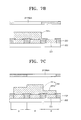
- FIG. 10C is a plan view schematically illustrating a mask for depositing red-blue intermediate layers of the organic light-emitting display device of FIG. 10A .
- FIG. 10A schematically illustrates the intermediate layer pattern of the organic light-emitting display device, but may be considered to represent a plurality of sub-pixels, for convenience of explanation.
- the organic light-emitting display device includes a plurality of pixels, each including red, green, and blue sub-pixels sequentially arranged in one direction, e.g., in the x-axis direction, as indicated in FIG. 10A .
- the sub-pixels are arranged such that the colors of the light emitted from the respective sub-pixels of a first pixel are symmetrical with the colors emitted from corresponding sub-pixels of a second pixel facing the first pixel in the x-axis direction, about the boundary between the first and second pixels. That is, for example, the sub-pixels of the pixels in the x-axis direction are arranged in the order of green, red, blue, blue, red, green, etc.
- the organic light-emitting display device is different from the first and second embodiments, in terms of an intermediate layer shape.
- Each of the sub-pixels includes a first electrode and a second electrode that face each other and an intermediate layer interposed between the first and second electrodes.
- an intermediate layer is formed as one piece, across two sub-pixels that are adjacent in the x-axis direction. More specifically, in the intermediate layer pattern (sub-pixel pattern) illustrated in FIG.
- the first pixel 311 includes a sub-pixel 311G (green sub-pixel), a sub-pixel 311R (red sub-pixel), and a sub-pixel 311B (blue sub-pixel).
- a plurality of sub-pixels 312B, 312R, and 312G of the second pixel 312, which is adjacent to the first pixel 311, are arranged to be symmetrical with respect to the sub-pixels 311 G, 311R, and 311B of the first pixel 311, along the boundary between the first and second pixels 311 and 312.
- the second pixel 312 includes the sub-pixel 312B, the sub-pixel 312R, and the sub-pixel 312G.
- an intermediate layer is formed as one piece, in sub-pixels adjacent at the boundary between the first and second pixels 311 and 312. That is, an intermediate layer 311RB is formed as one piece across red and blue sub-pixels 311R and 311 B of the first pixel 311.
- An intermediate layer 312RB is formed as one piece across red and blue sub-pixels 312R and 312B of the second pixel 312.
- an intermediate layer is formed as one piece across sub-pixels adjacent to the boundary between the second pixel 312 and the third pixel 313. That is, an intermediate layer 312RG is formed as one piece for red and green sub-pixels.
- An intermediate layer 313RG is formed as one piece across red and green sub-pixels in the third pixel 313.
- the other pixels in the x-axis direction also have the above-described pattern.
- a mask 310RGm illustrated in FIG. 10B is used to form an intermediate layer for red and green sub-pixels.
- a mask 310RBm illustrated in FIG. 10C is used to form an intermediate layer for red and blue sub-pixels. Referring to FIGS. 10B and 10C , the sizes of openings in the masks 310RGm and 310RBm are relatively large.
- the mask 310RGm illustrated in FIG. 10B is used to deposit an intermediate layer according to the arrangement of sub-pixels in the organic light-emitting display device.
- the area of each of the openings in the mask 310RGm is approximately four times larger than the openings in the conventional mask 10Bm illustrated in FIG. 1B . Accordingly, a high-definition organic light-emitting display device can be realized.
- a light-emitting device that can be included in the organic light-emitting display devices is formed on a substrate 602.
- the substrate 602 is manufactured using a transparent glass material, but may be manufactured using various plastic materials, such as acryl, polyimide, polycarbonate, polyester, and MYLAR.
- the light-emitting device may have various shapes.
- the light-emitting device may be a passive matrix (PM) light-emitting device, or may be an active matrix (AM) light-emitting device that has a thin transistor.
- PM passive matrix
- AM active matrix
- FIG. 11 is a cross-sectional view of a PM light-emitting device 603, according to an embodiment of the present invention.
- a buffer layer 621 SiO 2 layer
- a plurality of first electrodes 631 are formed in a predetermined pattern on the buffer layer 621.
- an emission layer 633 and a plurality of second electrodes 634 are sequentially formed on the first electrodes 631.
- An insulating layer 632 may be interposed between lines of the first electrodes 631.
- the second electrodes 634 may be formed in a pattern orthogonal to the pattern of the first electrodes 631.
- an additional insulating layer may further be included as a pattern orthogonal to the first electrodes 631, in order to obtain the pattern of the second electrodes 634.
- the emission layer 633 may be formed of an organic material or an inorganic material.
- a small molecule organic material or a polymer organic material, may be used. If a small molecule organic material is used, a hole injection layer (HIL), a hole transport layer (HTL), an organic emission layer (EML), an electron transport layer (ETL), and an electron injection layer (EIL) may be stacked in a single or composite structure.
- Various organic materials such as copper phthalocyanine (CuPc), N,N'-Di(naphthalene-1-yl)-N,N'-diphenyl-benzidine (NPB), and tris-8-hydroxyquinoline aluminum (Alq3), can be used.
- CuPc copper phthalocyanine
- NPB N,N'-Di(naphthalene-1-yl)-N,N'-diphenyl-benzidine
- Alq3 tris-8-hydroxyquinoline aluminum
- the emission layer 633 is formed of a polymer organic material, it includes the hole transport layer and the emission layer.
- the hole transport layer is formed of Poly(3,4-ethylenedioxythiophene) poly(styrenesulfonate) (PEDOT), and the emission layer is formed of a Poly-Phenylenevinylene (PPV)/ Polyfluorene-based polymer organic material.
- PEDOT Poly(3,4-ethylenedioxythiophene) poly(styrenesulfonate)
- the emission layer is formed of a Poly-Phenylenevinylene (PPV)/ Polyfluorene-based polymer organic material.
- the first electrodes 631 can be anode electrodes, and the second electrodes 634 can be cathode electrodes, and vice versa.
- the first electrodes 631 may be transparent electrodes or reflective electrodes. If the first electrodes 631 are transparent electrodes, ITO, IZO, ZnO, or In 2 O 3 may be used. If the first electrodes 631 are reflective electrodes, first electrodes 631 are obtained by forming a reflective layer, by using Ag, Mg, Al, Pt, Pd, Au, Ni, Nd, Ir, Cr, or a compound thereof and then depositing a layer made of ITO, IZO, ZnO, or In 2 O 3 on the resultant structure.
- the second electrodes 634 may also be transparent electrodes or reflective electrodes. If the second electrodes 634 are transparent electrodes, the second electrodes 634 can be used as cathode electrodes. Thus, the second electrodes 634 may be obtained by depositing a metal material having a small work function, such as Li, Ca, LiF/Ca, LiF/Al, Al, Mg, or a compound thereof on the emission layer 633, which is an organic layer. Auxiliary electrodes or a butt electrode lines can be then formed by using a material, such as ITO, IZO, ZnO, or In 2 O 3 . If the second electrodes 634 are reflective electrodes, they can be formed by depositing Li, Ca, LiF/Ca, LiF/Al, Al, Mg, or a compound thereof.
- FIG. 12 is a cross-sectional view of an AM light-emitting device 603, according to an embodiment of the present invention.
- each sub-pixel includes at least one thin film transistor (TFT), as illustrated in FIG. 12 .
- TFT thin film transistor
- the construction of the TFT is not limited to the one illustrated in FIG. 12 , and a total number and construction of thin transistors TFT can vary.
- a buffer layer 621 made of SiO 2 is formed on a glass substrate 602, and the TFT is formed on the buffer layer 621.
- the TFT includes an active layer 622 on the buffer layer 621, a gate insulating layer 623 on the active layer 622 and the buffer layer 621, and a gate electrode 624 on the gate insulating layer 623.
- the gate electrode 624 is formed at a predetermined location, on the gate insulating layer 623, and is connected to a gate line that transfers an on/off signal of the TFT.
- the predetermined location on which the gate electrode 624 is formed corresponds to a channel region in the active layer 622.
- An inter-insulator 625 is formed on the gate electrode 624.
- a source electrode 626 and a drain electrode 627 are formed to respectively contact a source region and a drain region of the active layer 622, via a contact hole.
- a passivation layer 628 made of SiO 2 is formed on the source electrode 626 and the drain electrode 627.
- a pixel defining layer 629 made of acryl or polyimide is formed on the passivation layer 628, and can protect the TFT, and also can planarize an upper surface of the TFT.
- At least one capacitor is connected to the TFT.
- a circuit having such the TFT is not limited to the one illustrated in FIG. 12 .
- the AM light-emitting device 603 is connected to the drain electrode 627 of the TFT.
- a first electrode 631 of the AM light-emitting device is formed on the passivation layer 628, and the pixel defining layer 629 is formed on the first electrode 631.
- An emission layer 633 is formed in an opening of the pixel defining layer 629.
- FIG. 12 illustrates that the emission layer 633 is patterned to correspond to only one sub-pixel, in order to explain the construction of each of the sub-pixels, for convenience, but the emission layer 633 may extend to an adjacent sub-pixel.
- the AM light-emitting device 603 is sealed on the substrate 602 an opposite unit (not shown).
- the opposite unit may include a glass or plastic material, or may be formed as a metal cap.
- intermediate layers are constructed as described above, and thus, pattern precision can be improved, while easily depositing an intermediate layer in each sub-pixel, thereby increasing the resolution of the light-emitting display device.
- a display device has the following advantages.
Landscapes
- Physics & Mathematics (AREA)
- Optics & Photonics (AREA)
- Engineering & Computer Science (AREA)
- Geometry (AREA)
- Microelectronics & Electronic Packaging (AREA)
- Manufacturing & Machinery (AREA)
- Electroluminescent Light Sources (AREA)
- Devices For Indicating Variable Information By Combining Individual Elements (AREA)
Abstract
Description
- Aspects of the present invention relate to an organic light-emitting display device and a method of manufacturing the same, and more particularly, to an organic light-emitting display device including an easily and precisely deposited intermediate layer, and a method of manufacturing the same.
- Organic light-emitting display devices are considered to be the next-generation of display devices, since they have a wide viewing angle, a high contrast, and a quick response speed. In general, an organic light-emitting display device has a stacked structure, in which an emission layer is interposed between an anode and a cathode. A color display can thereby be realized, based on a principle that light is emitted, by reuniting holes injected from the anode and electrons injected from the cathode, on the emission layer. However, such a structure makes it difficult to achieve efficient light emission. Thus, intermediate layers, such as an electron injection layer, an electron transport layer, a hole transport layer, and a hole injection layer, are selectively inserted between each of the electrodes and the emission layer.
- However, it difficult to finely pattern a thin organic layer, such as an emission layer, or an intermediate layer, and the luminous efficiencies of red, green, and blue sub-pixels depend on the organic layers being precisely patterned. Thus, a conventional organic light-emitting display device should be improved, since it is difficult to achieve a desirable driving voltage, current density, brightness, color purity, luminous efficiency, and lifetime.
- An organic light-emitting display device can also be structured to include an emission layer and an intermediate layer, between a first electrode and a second electrode. In this case, the first and second electrodes and the intermediate layer may be fabricated in various ways, e.g., by a deposition method. In order to manufacture an organic light-emitting display device according to the deposition method, a thin layer is formed in a predetermined pattern, by closely adhering a mask, having the same pattern as the thin layer, to a plane on which the thin layer is to be formed, and then depositing a material for the thin layer, on the resultant structure.
-
FIG. 1A is a plan view schematically illustrating an emission layer/intermediate layer pattern of a conventional organic light-emittingdisplay device 10.FIG. 1B is a plan view schematically illustrating a mask 10Bm for depositing a blue emission layer of the conventional organic light-emittingdisplay device 10. Referring toFIGS. 1A and1B ,pixels emitting display device 10 respectively include a plurality ofemission layers - As described above, the
emission layers 11 R through 14B of thepixels 11 through 14 are formed through deposition, using a mask. For example, the emission layers of red sub-pixels are simultaneously formed through deposition, the emission layers of green sub-pixels are simultaneously formed through deposition, and then the emission layers of blue sub-pixels are simultaneously formed through deposition.
Thus, the conventional mask 10Bm having a plurality ofopenings 11 Bm, 12Bm, 13Bm, and 14Bm, as illustrated inFIG. 1B , is used to obtain a blue emission layer pattern of the conventional organic light-emitting display device 10, as illustrated inFIG. 1A . Also, a mask having a plurality of openings formed at the same intervals as in the conventional mask 10Bm needs to be used, in order to form each red and green emission layer pattern of the organic light-emitting display device 10. - Since the intermediate layer is also formed in the same pattern as the emission layer, a mask having a plurality of openings formed at the same intervals as in the conventional mask 10Bm needs to be used, in order to obtain an intermediate layer pattern of the organic light-
emitting display device 10. However, as the distances between sub-pixels become smaller, in order to manufacture high-definition display devices, the sizes of the openings of the masks become smaller. That is, referring toFIG. 1B , the widths ℓ0 of the openings 11Bm through 14Bm become smaller. Thus, a mask having smaller openings is used, in order to realize a high-definition organic light-emitting display device. However, there is a limit as to how fine-pitched a mask can be. - Also, as a mask pattern becomes finer, it is more difficult to pattern the mask and align the mask with respect to a region on which an emission layer/intermediate layer is to be deposited. Even a slight error may cause an emission layer to overlap an adjacent emission layer. Furthermore, display devices, other than an organic light-emitting display device, manufactured through such deposition, also have the above-described disadvantages.
- Aspects of the present invention provide a display device, in which an intermediate layer of each sub-pixel can be easily and precisely deposited.
- According to an aspect of the present invention, there is provided an organic light-emitting display device including a plurality of pixels. Each of the pixels comprises a red, a green, and a blue sub-pixel. The display device includes an intermediate layer that is formed to different thicknesses in the respective sub-pixels.
- According to aspects of the present invention, in each pixel, the red sub-pixel may be arranged between the blue and green sub-pixels. The thickness of the intermediate layer may be at a maximum in the red sub-pixels.
- According to aspects of the present invention, the sum of the thickness of the intermediate layer of the green sub-pixel and the thickness of the intermediate layer of the blue sub-pixel may be substantially equal to the thickness of the intermediate layer in the red sub-pixel.
- According to aspects of the present invention, an intermediate layer may be formed as one piece, within each of the pixels.
- According to aspects of the present invention, each of the sub-pixels may further comprise: opposing first and second electrodes; an intermediate layer disposed between the electrodes; and red, green, and blue emission layers disposed within the intermediate layer. The thickness of the intermediate layer in a region having the red emission layer is greater than of at least one of a region having the green emission layer and a region having the blue emission layer.
- According to aspects of the present invention, the sub-pixels included in the adjacent pixels may be arranged such that the respective sub-pixels of a pixel are symmetrical with respect to a boundary between the adjacent pixels.
- According to aspects of the present invention, an intermediate layer may be formed as one piece, and can extend across adjacent pixels.
- According to aspects of the present invention, the intermediate layer may comprise: a hole injection layer formed within each of the pixels to a generally constant thickness; and a hole transport layer formed on the hole injection layer, having a thickness that varies according to the respective sub-pixels.
- According to aspects of the present invention, the intermediate layer may comprise: a hole injection layer having a thickness that varies according to the respective sub-pixels; and a hole transport layer formed on the hole injection layer, having a uniform thickness.
- According to aspects of the present invention, the intermediate layer may comprise: a hole injection layer having a thickness that varies according to the respective sub-pixels; and a hole transport layer formed on the hole injection layer, having a thickness that varies according to the respective sub-pixels.
- According to aspects of the present invention, the intermediate layer may comprise an electron transport layer having a thickness that varies according to the respective sub-pixels.
- According to another aspect of the present invention, there is provided a method of manufacturing an organic light-emitting display device having a plurality of pixels, each having red, green, and blue sub-pixels, the method comprising: forming a plurality of first electrodes on a surface of a substrate; forming an emission layer and an intermediate layer on the first electrode, having a thickness that varies according to the respective sub-pixels; and forming a plurality of second electrodes on the emission layer and the intermediate layer.
- According to aspects of the present invention, the forming of the intermediate layer may comprise: depositing a first portion of the intermediate layer in a first region; and depositing a second portion of the intermediate layer in a second region, which partly overlaps the first region.
- According to aspects of the present invention, the forming of the emission layer may comprise forming a red emission layer in a region where the first region and the second region overlap each other.
- According to aspects of the present invention, the forming of the intermediate layer may comprise: forming the intermediate layer, as one piece, in a region having the red and green sub-pixels; and forming the intermediate layer, as one piece, in a region having the red and green sub-pixels.
- According to aspects of the present invention, the forming of the intermediate layer, as one piece, in the region having the red and green sub-pixels, comprises patterning the intermediate layer by using a first mask, in which the region having the red and green sub-pixels is formed as one opening.
- According to aspects of the present invention, the forming of the intermediate layer, as one piece, in the region having the red and blue sub-pixels, may comprise patterning the intermediate layer by using a second mask, in which the region having the red and blue sub-pixels is formed as one opening.
- According to aspects of the present invention, the forming of the intermediate layer may comprise forming an intermediate layer, as one piece, within each of the pixels.
- According to aspects of the present invention, the forming of the emission layer and the intermediate layer may comprise: forming an intermediate layer on the first electrode, such that the thickness of a part of the intermediate layer varies according to sub-pixels; and forming an emission layer on the intermediate layer.
- According to aspects of the present invention, the forming of the intermediate layer may comprises: forming a hole injection layer on the first electrode to a generally constant thickness; and forming a hole transport layer on the hole injection layer, such that the thickness of a part of the hole transport layer varies according to sub-pixels.
- According to aspects of the present invention, the forming of the intermediate layer may comprise: forming a hole injection layer on the first electrode, such that the thickness of a part of the hole injection layer varies according to sub-pixels.
- According to aspects of the present invention, the forming of the intermediate layer may comprises: forming a hole injection layer on the first electrode, such that the thickness of the hole injection layer varies according to sub-pixels; and forming a hole transport layer on the hole injection layer, such that the thickness of the hole transport layer varies according to the sub-pixels.
- According to aspects of the present invention, the forming of the emission layer and the intermediate layer may comprise: forming an emission layer on the first electrode; and forming an intermediate layer on the emission layer, such that the thickness the intermediate layer varies according to sub-pixels.
- According to aspects of the present invention, the forming of the intermediate layer may comprise forming an electron transport layer on the emission layer, such that the thickness of the electron transport layer varies according to sub-pixels.
- According to another aspect of the present invention, there is provided an organic light-emitting display device comprising: a substrate; opposing first and second electrodes disposed on the substrate; and an intermediate layer disposed between the electrodes; and a plurality of emission layers disposed in the intermediate layer. A red emission layer is arranged between blue and green emission layers at the center of one pixel. The thickness of an intermediate layer is at a maximum adjacent to the red emission layer.
- According to aspects of the present invention, the intermediate layer may comprise at least one of a hole injection layer, a hole transport layer, and an electron transport layer.
- According to aspects of the present invention, the intermediate layer may be formed as one piece within each pixel.
- According to aspects of the present invention, the first electrode may be a reflective electrode, and the second electrode may be a semi-transparent electrode, or a transparent electrode.
- According to aspects of the present invention, a resonance may occur between the first electrode and the second electrode, when the device is driven.
- Additional aspects and/or advantages of the invention will be set forth in part in the description which follows and, in part, will be obvious from the description, or may be learned by practice of the invention.
- These and/or other aspects and advantages of the invention will become apparent and more readily appreciated from the following description of the embodiments, taken in conjunction with the accompanying drawings of which:
-
FIG. 1A is a plan view schematically illustrating an emission layer/intermediate layer pattern of a conventional organic light-emitting display device; -
FIG. 1B is a plan view schematically illustrating a conventional mask for depositing a blue emission layer of the organic light-emitting display device ofFIG. 1A ; -
FIG. 2 is a cross-sectional view of an organic light-emitting display device, according to a first embodiment of the present invention; -
FIGS. 3A through 3E are cross-sectional views sequentially illustrating a method of manufacturing the organic light-emitting display device, according to the first embodiment of the present invention; -
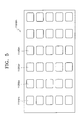
FIGS. 4 and5 are plan views schematically illustrating masks for depositing intermediate layers of an organic light-emitting display device; -
FIG. 6 is a cross-sectional view of an organic light-emitting display device, according to a second embodiment of the present invention; -
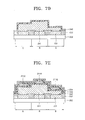
FIGS. 7A through 7E are cross-sectional views sequentially illustrating a method of manufacturing the organic light-emitting display device, according to the second embodiment of the present invention; -
FIG. 8 is a cross-sectional view of an organic light-emitting display device, according to a third embodiment of the present invention; -
FIGS. 9A through 9E are cross-sectional views sequentially illustrating a method of manufacturing the organic light-emitting display device according to the third embodiment of the present invention; -
FIG. 10A is a plan view schematically illustrating an intermediate layer pattern of an organic light-emitting display device, according to a fourth embodiment of the present invention; -
FIG. 10B is a plan view schematically illustrating a mask for depositing red-green intermediate layers of the organic light-emitting display device ofFIG. 10A , according to an embodiment of the present invention; -
FIG. 10C is a plan view schematically illustrating a mask for depositing red-blue intermediate layers of the organic light-emitting display device ofFIG. 10A , according to an embodiment of the present invention; -
FIG. 11 is a cross-sectional view of a passive matrix (PM) light-emitting device, according to an embodiment of the present invention; and -
FIG. 12 is a cross-sectional view of an active matrix (AM) light-emitting device, according to an embodiment of the present invention. - Reference will now be made in detail to embodiments of the present invention, examples of which are illustrated in the accompanying drawings, wherein like reference numerals refer to the like elements throughout. The embodiments are described below, in order to explain the aspects of the present invention, by referring to the figures. As referred to herein, when a first element is said to be disposed or formed "on", or "adjacent to", a second element, the first element can directly contact the second element, or can be separated from the second element by one or more other elements can be located therebetween. In contrast, when an element is referred to as being disposed "directly on" another element, there are no intervening elements present. As used herein, the term "and/or" includes any and all combinations of one or more of the associated listed items.
-
FIG. 2 is a cross-sectional view of an organic light-emitting display device, according to a first embodiment of the present invention. Referring toFIG. 2 , the organic light-emitting display device includes asubstrate 102,first electrodes 131, an insulatinglayer 132,second electrodes 134, emission layers (EML) 111R (red emission layer), 111G (green emission layer), and 111B (blue emission layer), and an intermediate layer that is formed on the top and/or bottom of the emission layers 111 R, 111G, and 111B. The intermediate layer includes a hole injection layer (HIL) 141, a hole transport layer (HTL) 142, and an electron transport layer (ETL) 143 The emission layers 111R, 111G, 111B, and the HIL, HTL, andETL first electrodes 131 and thesecond electrodes 134. The emission layers 111R, 111G, and 111B may emit red, green, or blue light, according to a material thereof, respectively. - The
first electrodes 131 are patterned on thesubstrate 102. Then, the insulatinglayer 132 is formed to fill gaps between thefirst electrodes 131, thus defining pixel regions. TheHIL 141, theHTL 142, the emission layers 111R, 111G, and 111B, theETL 143, and an electron injection layer (EIL) (not shown) are deposited on thefirst electrodes 131, as a single or a composite structure. Then, thesecond electrodes 134 are formed on theETL 143. - One of the
first electrodes 131 or thesecond electrodes 134 are reflective electrodes and the others are semi-transparent or transparent electrodes. Thus, a resonance may occur between thefirst electrodes 131 and thesecond electrodes 134, when the organic light-emitting display device is driven. Thus, light generated by the emission layers 111R, 111G, and 111B, when the organic light-emitting display device is driven, is emitted outside the organic light-emitting display device, while resonating between thefirst electrode 131 and thesecond electrode 134. Accordingly, the brightness and efficiency of light emission may be improved. - More specifically, the
first electrodes 131 may be formed on a surface of thesubstrate 102. In the present embodiment, thefirst electrodes 131 may be reflective electrodes, and thesecond electrodes 134 may be semi-transparent or transparent electrodes. Thus, light generated by the emission layers 111R, 111G, and 111B may be emitted outside the organic light-emitting display device (in the opposite direction of the substrate102), via thesecond electrodes 134, while resonating between the first andsecond electrodes - An intermediate layer of an organic light-emitting display device, according to an embodiment of the present invention, may include the
HIL 141 or theHTL 142, or may include a single layer having hole injection and transport characteristics. - The organic light-emitting display device, according to the first embodiment, is manufactured in such a manner that an intermediate layer including the
HIL 141 or theHTL 142 is deposited at different thicknesses on different sub-pixels. More specifically, theHTL 142 may be formed to a thickness of 1600 Å to 2200 Å in a red sub-pixel R. If the thickness of theHTL 142 is less than 1600 Å, or greater than 2200 Å, theemission layer 111R may not have appropriate hole injection characteristics and/or hole transport characteristics, so as to cause the resonance, and thus, the degree of color purity and the luminous efficiency may be degraded. If the thickness of theHTL 142 is greater than 2200 Å, a driving voltage may increase. - In a green sub-pixel G, the
HTL 142 may be formed to a thickness of 1000 Å to 1200 Å. If the thickness of theHTL 142 is less than 1000 Å, or greater than 1200 Å, theemission layer 111G may not have appropriate hole injection characteristics and/or hole transport characteristics, to cause the resonance, and thus, the degree of color purity and the luminous efficiency may be degraded. If the thickness of theHTL 142 is greater than 1200 Å, the driving voltage may increase. - In a blue sub-pixel B, the
HTL 142 may be formed to a thickness of 100 Å to 500 Å. If the thickness of theHTL 142 is less than 100 Å, or greater than 500 Å, theemission layer 111B may not have appropriate hole injection characteristics and/or hole transport characteristics, to cause the resonance, and thus, the degree of color purity and the luminous efficiency may be degraded. If the thickness of theHTL 142 is greater than 500 Å, the driving voltage may increase. - In the present embodiment, the
HTL 142 is formed, as one piece, in the red sub-pixel R and the green red sub-pixel G, and then is formed again, as one piece, in the red sub-pixel and a blue red sub-pixel B. That is, theHTL 142 is deposited on the green and blue sub-pixels G and B only once, but is deposited on the red sub-pixel R twice. Thus, the thickness of theHTL 142 in the red sub-pixel R is greater than in the green and blue sub-pixels G and B. In other words, the thickness of theHTL 142 in the red sub-pixel R is substantially equal to the sum of the thickness of theHTL 142 in the green sub-pixel G and the thickness of theHTL 142 in the blue sub-pixel B. Also, theHTL 142 is formed as one piece within one pixel. - As described above, in an organic light-emitting display device, according to an embodiment of the present invention, resonance may occur between first and second electrodes, when the organic light-emitting display device is driven. In this case, the thickness of a hole transport layer varies, according to the color of light emitted from an emission layer, thereby achieving good driving voltage, current density, brightness of light emission, degree of color purity, luminous efficiency, lifetime, and so on.
-
FIGS. 3A through 3E are cross-sectional views schematically and sequentially illustrating a method of manufacturing the organic light-emitting display device, according to the first embodiment of the present invention. Referring toFIGS. 3A through 3E , the method includes forming thefirst electrodes 131 on the surface of thesubstrate 102, forming theHTL 142 on thefirst electrodes 131, so that the thickness of a part of theHTL 142 is greater than that of the remaining part thereof, forming the emission layers 111G, 111R, and 111B on theHTL 142, and formingsecond electrodes 134 on the emission layers 111G, 111R, and 111B. - More specifically, as illustrated in
FIG. 3A , thefirst electrodes 131 are formed on thesubstrate 102. Thesubstrate 102 can be any substrate used in the field of general organic light-emitting devices. For example, various types of substrates, such as a glass substrate, or a plastic substrate, can be used, in consideration of transparency, smoothness, tractability, water-resistance, and so on. - The
first electrodes 131 may be reflective electrodes, semi-transparent electrodes, or transparent electrodes formed using a conductive metal material selected from the group consisting of lithium (Li), magnesium (Mg), aluminum (Al), an aluminum-lithium alloy (Al-Li), calcium (Ca), a magnesium-indium alloy (Mg-In), a magnesium-silver alloy (Mg-Ag), and a calcium-aluminum alloy (Ca-Al), or a metal oxide material selected from the group consisting of an indium tin oxide (ITO), an indium zinc oxide (IZO), and an indium oxide (IN2O3). Otherwise, thefirst electrodes 131 may be formed using a combination of two or more materials selected from the conductive metals and the metal oxides. - The insulating
layer 132 is formed in a region in which an organic layer is to be formed. The insulatinglayer 132 can be formed in various ways, including a deposition method or a coating method, using an inorganic substance, such as a silicon oxide and a nitride, or an insulating organic substance. - As illustrated in
FIG. 3B , theHIL 141 is formed on thefirst electrodes 131 and the insulatinglayer 132, to a predetermined thickness. TheHIL 141 can be formed by various known methods, including a vacuum deposition method, a spin-coating method, a casting method, or a Langmuir-Blodget (LB) method. - As illustrated in
FIG. 3C , afirst HTL 142a is formed on theHIL 141, as one piece, in the red sub-pixel R and the green sub-pixel G. Then, as illustrated inFIG. 3D , asecond HTL 142b is formed on theHIL 141, as one piece, in the red sub-pixel R and the blue sub-pixel B. - In detail, as the distances between sub-pixels become smaller, in order to manufacture high-definition display devices, the sizes of openings of a mask for depositing emission layers/intermediate layers of the sub-pixels also becomes smaller. Thus, a fine-pitch mask having smaller openings is used in order to realize a high-definition organic light-emitting display. However there is a limit of the pitch of the mask.
- In order to solve the above problem, according to an embodiment of the present invention, an intermediate layer is deposited, as one piece, in two adjacent sub-pixel regions, i.e., in the red sub-pixel R and the green sub-pixel G, and on the red sub-pixel R, and the blue sub-pixel B.
- The optimal thickness of an intermediate layer varies according to the type of emission layer. The intermediate layer is the thickest at the red sub-pixel R. The green sub-pixel G and the blue sub-pixel B are arranged on either side of the red sub-pixel R. Then, an intermediate layer is formed, as one piece, in the red sub-pixel R and the green sub-pixel G, and then is formed again, as one piece, in the red sub-pixel R and the blue sub-pixel B. That is, the intermediate layer is formed only once in the green sub-pixel G and the blue sub-pixel B, but is formed twice in the red sub-pixel R. Accordingly, the thickness of the intermediate layer in the red sub-pixel R is greater than in the green and blue sub-pixels G and B. In other words, the thickness of the red sub-pixel R is substantially equal to the sum of the thickness of the intermediate layer in the green sub-pixel G and the thickness of the intermediate layer in the blue sub-pixel B.
- In the method of manufacturing the organic light-emitting display device, according to the first exemplary embodiment, masks 110RGm and 110RBm, as illustrated in
FIGS. 4 and5 , are used. When the masks 110RGm and 110RBm are used, the width ℓ1, of each of a plurality of openings 111RGm and 112RGm in the mask 110RGm and a plurality of openings 111RBm and 112RBm in the mask 110RBm, is approximately double the width ℓ0 of each of the openings 11Bm and 12Bm of the conventional mask 10Bm, illustrated inFIG. 1B . Accordingly, it is possible to lessen difficulties in manufacturing and alignment processes of a mask, thereby, increasing the yield and reducing costs in manufacturing a high-quality and high-definition display device. - As illustrated in
FIG. 3E , the emission layers 111R, 111G, and 111B are formed on theHTL 142. A material of the emission layers 111R, 111G, and 111B is not particularly limited. Then, theETL 143 is formed by vacuum-depositing or spin-coating an electron transport material on the emission layers 111R, 111G, and 111B. The electron transport material is not particularly limited and may be Alq3. Then, thesecond electrodes 134 are formed by depositing a material for a second electrode on theETL 143. The material for a second electrode may be a conductive, transparent, metal oxide selected from the group consisting of indium tin oxide (ITO), indium zinc oxide (IZO), tin oxide (SnO2), and a zinc oxide (ZnO). Otherwise, theETL 143 may be formed as a reflective electrode, a semi-transparent electrode, or a transparent electrode, by depositing a thin film using a metallic material selected from the group consisting of lithium (Li), magnesium (Mg), aluminum (Al), an aluminum-lithium alloy (Al-Li), calcium (Ca), a magnesium-indium alloy (Mg-In), a magnesium-silver alloy (Mg-Ag), and a calcium-aluminum alloy (Ca-Al). However, the material for a second electrode is not limited to the described materials. Thefirst electrodes 131 and thesecond electrodes 134 may respectively function as an anode and a cathode, and vice versa. - As described above, according to an embodiment of the present invention, a fine-pitch mask for forming intermediate layers can be easily manufactured, since the sizes of openings of the mask may be relatively large. Thus, a high-definition display device can be manufactured using the mask.
-
FIG. 6 is a cross-sectional view of an organic light-emitting display device, according to a second embodiment of the present invention.FIGS. 7A through 7E are cross-sectional views schematically and sequentially illustrating a method of manufacturing the organic light-emitting display device. - Referring to
FIGS. 6 and7 , the organic light-emitting display device includes asubstrate 202, a plurality offirst electrodes 231, an insulatinglayer 232, a plurality ofsecond electrodes 234, a plurality ofemission layers 211R (red emission layer), 211G (green emission layer), and 211B (blue emission layer), and an intermediate layer formed on the top and/or bottom of the emission layers 211R, 211G, and 211B. The intermediate layer includes ahole injection layer 241, ahole transport layer 242, and anelectron transport layer 243. The emission layers 211R, 211G, and 211B and the hole injection, hole transport, andelectron transport layers first electrodes 231 and thesecond electrodes 234. The emission layers 211R, 211G, and 211B may respectively emit red, green, or blue light depending on a material thereof. - The second embodiment is differs from the first embodiment in that the
hole injection layer 241 is formed to different thicknesses for different sub-pixels. In detail, thehole injection layer 241 is formed, as one piece, in a red sub-pixel R and a green sub-pixel G, and is formed again, as one piece, in the red sub-pixel R and a blue sub-pixel B. That is, thehole injection layer 241 is deposited only once in the green sub-pixel G and the blue sub-pixel B, but is deposited twice in the red sub-pixel R. Thus, the thickness of thehole injection layer 241 in the red sub-pixel R is greater than in the green and blue sub-pixels G and B. In other words, the thickness of thehole injection layer 241 in the red sub-pixel R is substantially equal to the sum of the thickness of thehole injection layer 241 in the green sub-pixel G and the thickness of thehole injection layer 241 in the blue sub-pixel B. Thehole injection layer 241 is formed as one piece within one pixel. To this end, as illustrated inFIG. 7A , thefirst electrodes 231 and an insulatinglayer 232 are formed on thesubstrate 202. - Then, as illustrated in
FIG. 7B , ahole injection layer 241 a is formed, as one piece, on thefirst electrodes 231 and the insulatinglayer 232, in both the red sub-pixel R and the green sub-pixel G. Then, as illustrated inFIG. 7C , ahole injection layer 241 b is formed, as one piece, on thefirst electrodes 231 and the insulatinglayer 232, in both the red sub-pixel R, and the blue sub-pixel B. - As illustrated in
FIG. 7D , thehole transport layer 242 is formed on thehole injection layer 241. Lastly, as illustrated inFIG. 7E , the emission layers 211R, 211G, and 211B, theelectron transport layer 243, and thesecond electrodes 234 are sequentially formed. As described above, a fine-pitch mask for forming intermediate layers can be easily made, since the sizes of openings can be relatively large, and a high-definition display device can be manufactured using the mask. - In the first embodiment, a hole injection layer is formed to a predetermined thickness for one pixel, and a hole transport layer is formed on the hole injection layer. The thickness of the hole transport layer can vary at different sub-pixels. In the second embodiment, a hole injection layer is formed to different thicknesses in different sub-pixels, and a hole transport layer is formed on the hole injection layer. However, the present invention is not limited thereto. That is, it is possible to derive from the first and second embodiments an organic light-emitting display device, including a hole injection layer formed to different thicknesses, and a hole transport layer that is formed on the hole injection layer, such that the thickness of the hole transport layer varies in different sub-pixels.
FIG. 8 is a cross-sectional view of an organic light-emitting display device, according to a third embodiment of the present invention.FIGS. 9A through 9E are cross-sectional views sequentially illustrating a method of manufacturing the organic light-emitting display device. - Referring to
FIGS. 8 and9A through 9E , the organic light-emitting display device includes asubstrate 302, a plurality offirst electrodes 331, an insulatinglayer 332, a plurality ofsecond electrodes 334, a plurality of emission layers 311R, 311G, and 311B, and an intermediate layer. The intermediate layer can comprise ahole injection layer 341, ahole transport layer 342, and anelectron transport layer 343. The emission layers 311R, 311G, and 311B can be formed within the intermediate layer. The emission layers 311R, 311G, and 311B and the hole injection, hole transport, andelectron transport layers first electrodes 331 and thesecond electrodes 334. The emission layers 311R, 311G, and 311B can respectively emit red, green, or blue light, depending on a material thereof. - The third embodiment is differentiated from the first and second embodiments, in that the
electron transport layer 343 is formed to different thicknesses for different sub-pixels. In detail, theelectron transport layer 343 is deposited, as one piece, in both a red sub-pixel R and a green sub-pixel G, and then, is deposited, as one piece, in both the red sub-pixel R and a blue sub-pixel B. That is, theelectron transport layer 343 is deposited only once in the green and blue sub-pixels G and B, but is deposited twice in the red sub-pixel R. Thus, the thickness of theelectron transport layer 343 in the red sub-pixel R is greater than in the green and blue sub-pixels G and B. In other words, the thickness of theelectron transport layer 343 in the red sub-pixel R is substantially equal to the sum of the thickness of theelectron transport layer 343 in the green sub-pixel G and the thickness of theelectron transport layer 343 in the blue sub-pixel B. Theelectron transport layer 343 is formed as one piece within one pixel. - As illustrated in
FIG. 9A , thefirst electrodes 331 and the insulatinglayer 332 are formed on thesubstrate 302. Then, as illustrated inFIG. 9B , thehole injection layer 341 and thehole transport layer 342 are formed on thefirst electrodes 331 and the insulatinglayer 332. The emission layers 311R, 311G, and 311B are formed on thehole transport layer 342. Then, as illustrated inFIG. 9C , anelectron transport layer 343a is formed, as one piece, in the red sub-pixel R and the green sub-pixel G. - As illustrated in
FIG. 9D , anelectron transport layer 343b is formed, as one piece, in the red sub-pixel R and the blue sub-pixel B. Then, as illustrated inFIG. 9E , thesecond electrodes 334 are formed on theelectron transport layer 343. - As described above, according to an embodiment of the present invention, a fine-pitch mask for forming intermediate layers can be easily made, since the sizes of openings can be relatively large, and a high-definition display device can be manufactured using the mask.
-
FIG. 10A is a plan view of an intermediate layer pattern of an organic light-emitting display device, according to a fourth embodiment of the present invention.
FIG. 10B is a plan view schematically illustrating a mask for depositing red-green intermediate layers of the organic light-emitting display device ofFIG. 10A .FIG. 10C is a plan view schematically illustrating a mask for depositing red-blue intermediate layers of the organic light-emitting display device ofFIG. 10A . As described above,FIG. 10A schematically illustrates the intermediate layer pattern of the organic light-emitting display device, but may be considered to represent a plurality of sub-pixels, for convenience of explanation. - The organic light-emitting display device includes a plurality of pixels, each including red, green, and blue sub-pixels sequentially arranged in one direction, e.g., in the x-axis direction, as indicated in
FIG. 10A . The sub-pixels are arranged such that the colors of the light emitted from the respective sub-pixels of a first pixel are symmetrical with the colors emitted from corresponding sub-pixels of a second pixel facing the first pixel in the x-axis direction, about the boundary between the first and second pixels. That is, for example, the sub-pixels of the pixels in the x-axis direction are arranged in the order of green, red, blue, blue, red, green, green, red, blue, blue, red, green, etc. - The organic light-emitting display device according to the fourth embodiment is different from the first and second embodiments, in terms of an intermediate layer shape. Each of the sub-pixels includes a first electrode and a second electrode that face each other and an intermediate layer interposed between the first and second electrodes. In the organic light-emitting display device, according to the fourth embodiment, an intermediate layer is formed as one piece, across two sub-pixels that are adjacent in the x-axis direction. More specifically, in the intermediate layer pattern (sub-pixel pattern) illustrated in
FIG. 10A , if the plurality of pixels in the uppermost row are afirst pixel 311, asecond pixel 312, athird pixel 313, and afourth pixel 314 in the x-axis direction, thefirst pixel 311 includes a sub-pixel 311G (green sub-pixel), a sub-pixel 311R (red sub-pixel), and a sub-pixel 311B (blue sub-pixel). - A plurality of sub-pixels 312B, 312R, and 312G of the
second pixel 312, which is adjacent to thefirst pixel 311, are arranged to be symmetrical with respect to the sub-pixels 311 G, 311R, and 311B of thefirst pixel 311, along the boundary between the first andsecond pixels second pixel 312 includes the sub-pixel 312B, the sub-pixel 312R, and the sub-pixel 312G. - In the above intermediate layer pattern, an intermediate layer is formed as one piece, in sub-pixels adjacent at the boundary between the first and
second pixels blue sub-pixels first pixel 311. An intermediate layer 312RB is formed as one piece across red andblue sub-pixels second pixel 312. Similarly, an intermediate layer is formed as one piece across sub-pixels adjacent to the boundary between thesecond pixel 312 and thethird pixel 313. That is, an intermediate layer 312RG is formed as one piece for red and green sub-pixels. An intermediate layer 313RG is formed as one piece across red and green sub-pixels in thethird pixel 313. Similarly, the other pixels in the x-axis direction also have the above-described pattern. - In this case, a mask 310RGm illustrated in
FIG. 10B is used to form an intermediate layer for red and green sub-pixels. A mask 310RBm illustrated inFIG. 10C is used to form an intermediate layer for red and blue sub-pixels. Referring toFIGS. 10B and10C , the sizes of openings in the masks 310RGm and 310RBm are relatively large. - The mask 310RGm illustrated in
FIG. 10B is used to deposit an intermediate layer according to the arrangement of sub-pixels in the organic light-emitting display device. The area of each of the openings in the mask 310RGm is approximately four times larger than the openings in the conventional mask 10Bm illustrated inFIG. 1B . Accordingly, a high-definition organic light-emitting display device can be realized. - The construction of a light-emitting device having the above intermediate layers, which can be included in the organic light-emitting display devices according to the above embodiments, will now be briefly described with reference to
FIGS. 11 and 12 . A light-emitting device that can be included in the organic light-emitting display devices is formed on asubstrate 602. Thesubstrate 602 is manufactured using a transparent glass material, but may be manufactured using various plastic materials, such as acryl, polyimide, polycarbonate, polyester, and MYLAR. - The light-emitting device may have various shapes. For example, the light-emitting device may be a passive matrix (PM) light-emitting device, or may be an active matrix (AM) light-emitting device that has a thin transistor.
-
FIG. 11 is a cross-sectional view of a PM light-emittingdevice 603, according to an embodiment of the present invention. Referring toFIG. 6 , a buffer layer 621 (SiO2 layer) is formed on thesubstrate 602. A plurality offirst electrodes 631 are formed in a predetermined pattern on thebuffer layer 621. Then, anemission layer 633 and a plurality ofsecond electrodes 634 are sequentially formed on thefirst electrodes 631. An insulatinglayer 632 may be interposed between lines of thefirst electrodes 631. Thesecond electrodes 634 may be formed in a pattern orthogonal to the pattern of thefirst electrodes 631. Although not shown in the drawings, an additional insulating layer may further be included as a pattern orthogonal to thefirst electrodes 631, in order to obtain the pattern of thesecond electrodes 634. - The
emission layer 633 may be formed of an organic material or an inorganic material. When theemission layer 633 is formed of an organic material, a small molecule organic material, or a polymer organic material, may be used. If a small molecule organic material is used, a hole injection layer (HIL), a hole transport layer (HTL), an organic emission layer (EML), an electron transport layer (ETL), and an electron injection layer (EIL) may be stacked in a single or composite structure.
Various organic materials, such as copper phthalocyanine (CuPc), N,N'-Di(naphthalene-1-yl)-N,N'-diphenyl-benzidine (NPB), and tris-8-hydroxyquinoline aluminum (Alq3), can be used. Theemission layer 633 is obtained by patterning one of the above small molecule organic materials, and vacuum-depositing the resultant structure using one of the above masks. - In general, if the
emission layer 633 is formed of a polymer organic material, it includes the hole transport layer and the emission layer. In this case, the hole transport layer is formed of Poly(3,4-ethylenedioxythiophene) poly(styrenesulfonate) (PEDOT), and the emission layer is formed of a Poly-Phenylenevinylene (PPV)/ Polyfluorene-based polymer organic material. - The
first electrodes 631 can be anode electrodes, and thesecond electrodes 634 can be cathode electrodes, and vice versa. Thefirst electrodes 631 may be transparent electrodes or reflective electrodes. If thefirst electrodes 631 are transparent electrodes, ITO, IZO, ZnO, or In2O3 may be used. If thefirst electrodes 631 are reflective electrodes,first electrodes 631 are obtained by forming a reflective layer, by using Ag, Mg, Al, Pt, Pd, Au, Ni, Nd, Ir, Cr, or a compound thereof and then depositing a layer made of ITO, IZO, ZnO, or In2O3 on the resultant structure. - The
second electrodes 634 may also be transparent electrodes or reflective electrodes. If thesecond electrodes 634 are transparent electrodes, thesecond electrodes 634 can be used as cathode electrodes. Thus, thesecond electrodes 634 may be obtained by depositing a metal material having a small work function, such as Li, Ca, LiF/Ca, LiF/Al, Al, Mg, or a compound thereof on theemission layer 633, which is an organic layer. Auxiliary electrodes or a butt electrode lines can be then formed by using a material, such as ITO, IZO, ZnO, or In2O3. If thesecond electrodes 634 are reflective electrodes, they can be formed by depositing Li, Ca, LiF/Ca, LiF/Al, Al, Mg, or a compound thereof. -
FIG. 12 is a cross-sectional view of an AM light-emittingdevice 603, according to an embodiment of the present invention. In the AM light-emittingdevice 603, each sub-pixel includes at least one thin film transistor (TFT), as illustrated inFIG. 12 . The construction of the TFT is not limited to the one illustrated inFIG. 12 , and a total number and construction of thin transistors TFT can vary. - As illustrated in
FIG. 12 , abuffer layer 621 made of SiO2 is formed on aglass substrate 602, and the TFT is formed on thebuffer layer 621. The TFT includes anactive layer 622 on thebuffer layer 621, agate insulating layer 623 on theactive layer 622 and thebuffer layer 621, and agate electrode 624 on thegate insulating layer 623. Thegate electrode 624 is formed at a predetermined location, on thegate insulating layer 623, and is connected to a gate line that transfers an on/off signal of the TFT.
The predetermined location on which thegate electrode 624 is formed corresponds to a channel region in theactive layer 622. - An inter-insulator 625 is formed on the
gate electrode 624. Asource electrode 626 and adrain electrode 627 are formed to respectively contact a source region and a drain region of theactive layer 622, via a contact hole. - A
passivation layer 628 made of SiO2 is formed on thesource electrode 626 and thedrain electrode 627. Apixel defining layer 629 made of acryl or polyimide is formed on thepassivation layer 628, and can protect the TFT, and also can planarize an upper surface of the TFT. - Although not shown in the drawings, at least one capacitor is connected to the TFT. A circuit having such the TFT is not limited to the one illustrated in
FIG. 12 . - The AM light-emitting
device 603 is connected to thedrain electrode 627 of the TFT. Afirst electrode 631 of the AM light-emitting device is formed on thepassivation layer 628, and thepixel defining layer 629 is formed on thefirst electrode 631. Anemission layer 633 is formed in an opening of thepixel defining layer 629.
FIG. 12 illustrates that theemission layer 633 is patterned to correspond to only one sub-pixel, in order to explain the construction of each of the sub-pixels, for convenience, but theemission layer 633 may extend to an adjacent sub-pixel. - Materials of the first electrode 631 a
second electrode 634, theemission layer 633, and intermediate layers (not shown) formed on the top and bottom of theemission layer 633 may be the same as in the PM light-emittingdevice 603. The AM light-emittingdevice 603 is sealed on thesubstrate 602 an opposite unit (not shown). The opposite unit may include a glass or plastic material, or may be formed as a metal cap. - In a light-emitting display device having such light-emitting devices, intermediate layers are constructed as described above, and thus, pattern precision can be improved, while easily depositing an intermediate layer in each sub-pixel, thereby increasing the resolution of the light-emitting display device.
- The above embodiments of the present invention have been described with respect to a light-emitting display device, but aspects of the present invention can also be applied to any type of a display device, in which each sub-pixel is formed through deposition. A display device according to the above embodiments of the present invention has the following advantages.
- First, it is possible to lessen difficulties in manufacturing and alignment processes of a mask. Thus, it is possible to prevent the yield from decreasing, due to a reduction in the distances between sub-pixels. In is also possible to reduce manufacturing costs when manufacturing a high-quality and high definition display device. Second, it is possible to increases the sizes of openings in a mask for forming intermediate layers. Third, it is possible to easily make a fine-pitch mask, and manufacture a high-definition display device by using the mask.
- Although a few embodiments of the present invention have been shown and described, it would be appreciated by those skilled in the art that changes may be made in this embodiment without departing from the principles of the invention, the scope of which is defined in the claims and their equivalents.
Claims (26)
- An organic light-emitting display device comprising:pixels to emit light in a first direction, comprising a first electrode, a second electrode, and an intermediate layer disposed between the first and second electrodes, wherein,
each pixel is divided into red, green, and blue sub-pixels, and
the thickness of the intermediate layer varies according to the sub-pixels. - A device according to claim 1, wherein:in each of the pixels the red sub-pixel is disposed between the green and blue sub-pixels; andthe thickness of the intermediate layer is at a maximum in the red sub-pixel.
- A device according to claim 2, wherein the sum of the thicknesses of the intermediate layer in the blue and green sub-pixels is substantially equal to the thickness of the intermediate layer in the red sub-pixel.
- A device according to any preceding claim, wherein in each of the pixels the intermediate layer is formed as one piece.
- A device according to any preceding claim, wherein the red, green, and blue sub pixels respectively comprise red, green, and blue emission layers disposed in the intermediate layer,
wherein the thickness of the intermediate layer is at a maximum in the red sub-pixels. - A device according to any preceding claim, wherein the sub-pixels of adjacent pixels are symmetrically disposed according to color, about a boundary between the adjacent pixels.
- A device according to claim 6, wherein the intermediate layer is formed as one or more pieces that each extends across the boundary, so as to be disposed at least two of the adjacent pixels.
- A device according to any preceding claim, wherein the intermediate layer comprises:hole transport layers having thicknesses that vary according to the sub-pixels.
- A device according to any preceding claim, wherein the intermediate layer comprises:hole injection layers disposed on the first electrode in each pixel, having thicknesses that vary according to the sub-pixels.
- A device according to any preceding claim, wherein the intermediate layer comprises:hole injection layers having thicknesses that vary according to the sub-pixels; andhole transport layers formed on the hole injection layers, having thicknesses that vary according to the sub-pixels.
- A device according to any preceding claim, wherein the intermediate layer comprises electron transport layers having thicknesses that vary according to the sub-pixels.
- A method of manufacturing an organic light-emitting display device having a plurality of pixels that are each divided into red, green, and blue sub-pixels, the method comprising:forming first electrodes on a surface of a substrate;forming emission layers and an intermediate layer on the first electrodes, such that the thickness of the intermediate layer varies according to the sub-pixels; andforming a second electrode on the intermediate layer.
- A method according to claim 12, wherein the forming of the intermediate layer comprises:forming a first portion of the intermediate layer in a first region; andforming a second portion of the intermediate layer in a second region that overlaps the first region.
- A method according to Claim 13, wherein the forming of the emission layer comprises forming a red emission layer where the first region and the second region overlap.
- A method according to one of Claims 12 to 14, wherein the forming of the intermediate layer comprises:forming first portions of the intermediate layer across adjacent red and green sub-pixels; andforming second portions of the intermediate layer across adjacent blue and red sub-pixels, such that the first and second portions are joined together.
- A method according to Claim 15, wherein the forming of first portions of the intermediate layer comprises: using a first mask having openings that correspond to each of the first portions, to pattern the first portions.
- A method according to Claim 16, wherein the forming of the second portions of the intermediate layer comprises using a second mask having openings that correspond to each of the second portions, to pattern the second portions.
- A method according to one of Claims 12 to 17, wherein the forming of the intermediate layer comprises, in each of the pixels, forming the intermediate layer as one piece.
- A method according to one of Claims 12 to 18, wherein the forming of the emission layers and the intermediate layer comprises forming the emission layers within the intermediate layer.
- A method according to one of Claims 12 to 19, wherein the forming of the intermediate layer comprises:forming a hole injection layer on the first electrodes; andforming hole transport layers on the hole injection layer, such that the thicknesses of the hole transport layers vary according to the sub-pixels.
- A method according to one of Claims 12 to 20, wherein the forming of the intermediate layer comprises:forming hole injection layers on the first electrode, such that the thicknesses of the hole injection layers of vary according to the sub-pixels; andforming a hole transport layer on the hole injection layers.
- A method according to one of Claims 12 to 21, wherein the forming of the intermediate layer comprises:forming hole injection layers on the first electrodes, such that the thicknesses of the hole injection layers vary according to the sub-pixels; andforming hole transport layers on the hole injection layers, such that the thicknesses of the hole transport layers vary according to the sub-pixels.
- A method according to Claims 12 to 22, wherein the forming of the emission layer and the intermediate layer comprises:forming a first portion of the intermediate layer on the first electrodes;forming the emission layers on the first portion;forming a second portion of the intermediate layer on the emission layers, such that the thickness of the second portion varies according to the sub-pixels.
- A method according to Claim 23, wherein the second portion is an electron transport layer.
- A device according to one of Claims 1 to 11, wherein the green or blue sub-pixels of adjacent pixels are disposed at a boundary between the adjacent pixels.
- A device according to one of Claims 1 to 11 or Claim 25, wherein the thickness of the intermediate layer increases from the blue sub-pixel, to the green sub-pixel, to the red sub-pixel.
Applications Claiming Priority (1)
| Application Number | Priority Date | Filing Date | Title |
|---|---|---|---|
| KR1020080023413A KR100922763B1 (en) | 2008-03-13 | 2008-03-13 | Organic light emitting display device and manufacturing method thereof |
Publications (2)
| Publication Number | Publication Date |
|---|---|
| EP2101356A1 true EP2101356A1 (en) | 2009-09-16 |
| EP2101356B1 EP2101356B1 (en) | 2016-03-09 |
Family
ID=40756807
Family Applications (1)
| Application Number | Title | Priority Date | Filing Date |
|---|---|---|---|
| EP09250716.9A Active EP2101356B1 (en) | 2008-03-13 | 2009-03-13 | Organic light-emitting display apparatus and method of manufacturing the same |
Country Status (5)
| Country | Link |
|---|---|
| US (1) | US8344619B2 (en) |
| EP (1) | EP2101356B1 (en) |
| JP (1) | JP4989669B2 (en) |
| KR (1) | KR100922763B1 (en) |
| CN (1) | CN101533852B (en) |
Cited By (2)
| Publication number | Priority date | Publication date | Assignee | Title |
|---|---|---|---|---|
| EP2267778A3 (en) * | 2009-06-24 | 2011-09-14 | AU Optronics Corporation | Oled panel with broadened color spectral components |
| CN102270655A (en) * | 2010-06-03 | 2011-12-07 | 佳能株式会社 | display screen |
Families Citing this family (35)
| Publication number | Priority date | Publication date | Assignee | Title |
|---|---|---|---|---|
| TWI323047B (en) * | 2006-11-28 | 2010-04-01 | Univ Nat Taiwan | The method for forming electronic devices by using protection layers |
| JP5620146B2 (en) | 2009-05-22 | 2014-11-05 | 三星ディスプレイ株式會社Samsung Display Co.,Ltd. | Thin film deposition equipment |
| KR101127859B1 (en) * | 2009-05-27 | 2012-03-22 | 엘지디스플레이 주식회사 | Monochrome light emitting display device and method for driving the same |
| KR101094287B1 (en) * | 2009-10-09 | 2011-12-19 | 삼성모바일디스플레이주식회사 | Organic light emitting display |
| KR101084263B1 (en) * | 2009-12-14 | 2011-11-16 | 삼성모바일디스플레이주식회사 | Organic light emitting display |
| KR101084184B1 (en) | 2010-01-11 | 2011-11-17 | 삼성모바일디스플레이주식회사 | Thin film deposition apparatus |
| KR101182442B1 (en) * | 2010-01-27 | 2012-09-12 | 삼성디스플레이 주식회사 | OLED display apparatus and Method thereof |
| KR101084198B1 (en) * | 2010-02-24 | 2011-11-17 | 삼성모바일디스플레이주식회사 | Organic light emitting display |
| KR101663564B1 (en) * | 2010-03-26 | 2016-10-17 | 엘지디스플레이 주식회사 | Organic electro-luminescence device and method of fabricating the same |
| US8894458B2 (en) | 2010-04-28 | 2014-11-25 | Samsung Display Co., Ltd. | Thin film deposition apparatus, method of manufacturing organic light-emitting display device by using the apparatus, and organic light-emitting display device manufactured by using the method |
| KR101983229B1 (en) * | 2010-07-23 | 2019-05-29 | 삼성디스플레이 주식회사 | Organic light emitting device and method for manufacturing the same |
| CN102110707B (en) * | 2010-11-23 | 2013-07-03 | 友达光电股份有限公司 | Light emitting device and manufacturing method thereof |
| KR101838270B1 (en) * | 2011-05-25 | 2018-03-14 | 삼성디스플레이 주식회사 | Organic light emitting device |
| KR20130004830A (en) | 2011-07-04 | 2013-01-14 | 삼성디스플레이 주식회사 | Apparatus for thin layer deposition and method for manufacturing of organic light emitting display apparatus using the same |
| US8963420B2 (en) * | 2011-08-29 | 2015-02-24 | Lg Display Co., Ltd. | Organic electro-luminescence display panel for preventing the display panel from degrading and a method for fabricating the same |
| CN104160783B (en) * | 2012-03-07 | 2016-06-08 | 株式会社钟化 | The manufacture method of luminescent device and luminescent device |
| JP5988624B2 (en) * | 2012-03-09 | 2016-09-07 | キヤノン株式会社 | LIGHT EMITTING DEVICE, IMAGING DEVICE USING THE SAME, AND IMAGE FORMING DEVICE |
| KR102015872B1 (en) | 2012-06-22 | 2019-10-22 | 삼성디스플레이 주식회사 | Apparatus for organic layer deposition, method for manufacturing of organic light emitting display apparatus using the same, and organic light emitting display apparatus manufactured by the method |
| KR101469486B1 (en) | 2012-09-04 | 2014-12-05 | 엘지디스플레이 주식회사 | Organic light emitting display device |
| US9170665B2 (en) * | 2012-09-14 | 2015-10-27 | Universal Display Corporation | Lifetime OLED display |
| US9257665B2 (en) | 2012-09-14 | 2016-02-09 | Universal Display Corporation | Lifetime OLED display |
| JP6111643B2 (en) * | 2012-12-17 | 2017-04-12 | セイコーエプソン株式会社 | ORGANIC ELECTROLUMINESCENCE DEVICE AND ELECTRONIC DEVICE |
| KR102046157B1 (en) * | 2012-12-21 | 2019-12-03 | 삼성디스플레이 주식회사 | Organic light emitting diode display and manufacturing method thereof |
| KR102081284B1 (en) | 2013-04-18 | 2020-02-26 | 삼성디스플레이 주식회사 | Deposition apparatus, method for manufacturing organic light emitting display apparatus using the same, and organic light emitting display apparatus manufactured by the same |
| CN103337594B (en) | 2013-05-30 | 2016-02-10 | 京东方科技集团股份有限公司 | A kind of oled substrate and display unit |
| DE102014110271B4 (en) * | 2014-07-22 | 2017-11-02 | Osram Oled Gmbh | Optoelectronic component and method for producing an optoelectronic component |
| KR102552276B1 (en) * | 2015-02-24 | 2023-07-07 | 삼성디스플레이 주식회사 | Organic light emitting display device and manufacturing method of the same |
| KR102411542B1 (en) * | 2015-05-19 | 2022-06-22 | 삼성디스플레이 주식회사 | Pattern forming method for pixel and pixel position accuracy inspection and the mask for the same |
| CN107170909A (en) * | 2016-03-08 | 2017-09-15 | 昆山国显光电有限公司 | The preparation method of OLED display screen and its optical compensating layer |
| CN106129265B (en) * | 2016-09-09 | 2018-04-17 | 京东方科技集团股份有限公司 | Organic electroluminescence device |
| CN106601775B (en) * | 2016-12-19 | 2019-07-02 | 武汉华星光电技术有限公司 | OLED display device and manufacturing method thereof |
| CN107403878A (en) * | 2017-07-18 | 2017-11-28 | 广州新视界光电科技有限公司 | Preparation method, array base palte, display panel and the display device of array base palte |
| JP2019091807A (en) * | 2017-11-15 | 2019-06-13 | 株式会社ジャパンディスプレイ | Organic EL display |
| CN111540774B (en) * | 2020-05-09 | 2023-09-01 | 京东方科技集团股份有限公司 | Display panel, its manufacturing method and display device |
| WO2025243342A1 (en) * | 2024-05-20 | 2025-11-27 | シャープディスプレイテクノロジー株式会社 | Manufacturing method for display device, and display device |
Citations (5)
| Publication number | Priority date | Publication date | Assignee | Title |
|---|---|---|---|---|
| EP1052708A2 (en) | 1999-05-12 | 2000-11-15 | Pioneer Corporation | Organic electroluminescence multicolor display and method of fabricating the same |
| JP2004207126A (en) | 2002-12-26 | 2004-07-22 | Denso Corp | Organic EL panel |
| US20050280355A1 (en) | 2004-06-18 | 2005-12-22 | Kwan-Hee Lee | Organic light emitting display device and method of fabricating the same |
| US20070046195A1 (en) * | 2005-08-31 | 2007-03-01 | Univision Technology Inc. | Organic light-emitting display and fabricating method thereof |
| US20070296334A1 (en) | 2006-06-23 | 2007-12-27 | Canon Kabushiki Kaisha | Organic light-emitting device |
Family Cites Families (16)
| Publication number | Priority date | Publication date | Assignee | Title |
|---|---|---|---|---|
| US6384529B2 (en) * | 1998-11-18 | 2002-05-07 | Eastman Kodak Company | Full color active matrix organic electroluminescent display panel having an integrated shadow mask |
| TW594637B (en) | 2002-09-13 | 2004-06-21 | Sanyo Electric Co | Electroluminescence display device and method of pattern layout for the electroluminescence display device |
| JP4511119B2 (en) | 2003-01-27 | 2010-07-28 | 三洋電機株式会社 | Electroluminescence display device and pattern layout method of electroluminescence display device |
| US20040149984A1 (en) * | 2003-01-31 | 2004-08-05 | Eastman Kodak Company | Color OLED display with improved emission |
| JP4179119B2 (en) | 2003-09-19 | 2008-11-12 | ソニー株式会社 | Manufacturing method of organic light emitting device |
| TWI367686B (en) | 2004-04-07 | 2012-07-01 | Semiconductor Energy Lab | Light emitting device, electronic device, and television device |
| US7247394B2 (en) * | 2004-05-04 | 2007-07-24 | Eastman Kodak Company | Tuned microcavity color OLED display |
| US7023013B2 (en) * | 2004-06-16 | 2006-04-04 | Eastman Kodak Company | Array of light-emitting OLED microcavity pixels |
| KR100721554B1 (en) | 2004-07-22 | 2007-05-23 | 삼성에스디아이 주식회사 | Organic electroluminescent device and manufacturing method thereof |
| KR100683693B1 (en) | 2004-11-10 | 2007-02-15 | 삼성에스디아이 주식회사 | Light emitting device |
| JP4830328B2 (en) | 2005-03-25 | 2011-12-07 | セイコーエプソン株式会社 | Light emitting device |
| US8102111B2 (en) * | 2005-07-15 | 2012-01-24 | Seiko Epson Corporation | Electroluminescence device, method of manufacturing electroluminescence device, and electronic apparatus |
| KR101156426B1 (en) | 2005-08-25 | 2012-06-18 | 삼성모바일디스플레이주식회사 | An silsesquioxane-based compound and an organic light emitting device comprising the same |
| KR101272256B1 (en) | 2006-03-20 | 2013-06-13 | 삼성디스플레이 주식회사 | Container Member, Manufacturing Method of Container Member and Flat Panel Display Using the Same |
| KR100823511B1 (en) * | 2006-11-10 | 2008-04-21 | 삼성에스디아이 주식회사 | OLED display and manufacturing method thereof |
| TWI323047B (en) * | 2006-11-28 | 2010-04-01 | Univ Nat Taiwan | The method for forming electronic devices by using protection layers |
-
2008
- 2008-03-13 KR KR1020080023413A patent/KR100922763B1/en active Active
-
2009
- 2009-02-02 US US12/364,005 patent/US8344619B2/en active Active
- 2009-03-09 CN CN2009101184571A patent/CN101533852B/en active Active
- 2009-03-13 EP EP09250716.9A patent/EP2101356B1/en active Active
- 2009-03-13 JP JP2009061494A patent/JP4989669B2/en active Active
Patent Citations (5)
| Publication number | Priority date | Publication date | Assignee | Title |
|---|---|---|---|---|
| EP1052708A2 (en) | 1999-05-12 | 2000-11-15 | Pioneer Corporation | Organic electroluminescence multicolor display and method of fabricating the same |
| JP2004207126A (en) | 2002-12-26 | 2004-07-22 | Denso Corp | Organic EL panel |
| US20050280355A1 (en) | 2004-06-18 | 2005-12-22 | Kwan-Hee Lee | Organic light emitting display device and method of fabricating the same |
| US20070046195A1 (en) * | 2005-08-31 | 2007-03-01 | Univision Technology Inc. | Organic light-emitting display and fabricating method thereof |
| US20070296334A1 (en) | 2006-06-23 | 2007-12-27 | Canon Kabushiki Kaisha | Organic light-emitting device |
Cited By (3)
| Publication number | Priority date | Publication date | Assignee | Title |
|---|---|---|---|---|
| EP2267778A3 (en) * | 2009-06-24 | 2011-09-14 | AU Optronics Corporation | Oled panel with broadened color spectral components |
| US8183561B2 (en) | 2009-06-24 | 2012-05-22 | Au Optronics Corporation | OLED panel with broadened color spectral components |
| CN102270655A (en) * | 2010-06-03 | 2011-12-07 | 佳能株式会社 | display screen |
Also Published As
| Publication number | Publication date |
|---|---|
| JP2009224781A (en) | 2009-10-01 |
| KR20090098186A (en) | 2009-09-17 |
| EP2101356B1 (en) | 2016-03-09 |
| CN101533852A (en) | 2009-09-16 |
| CN101533852B (en) | 2013-07-03 |
| US8344619B2 (en) | 2013-01-01 |
| KR100922763B1 (en) | 2009-10-21 |
| JP4989669B2 (en) | 2012-08-01 |
| US20090231243A1 (en) | 2009-09-17 |
Similar Documents
| Publication | Publication Date | Title |
|---|---|---|
| EP2101356B1 (en) | Organic light-emitting display apparatus and method of manufacturing the same | |
| US11394015B2 (en) | Organic light-emitting display apparatus and method of manufacturing the same | |
| JP6254218B2 (en) | Organic light emitting display | |
| US9293515B2 (en) | Organic light-emitting display device and method of manufacturing the same | |
| CN101877357B (en) | Organic light emitting display apparatus | |
| KR101923172B1 (en) | Organic light emitting display apparatus and the method for manufacturing of the same | |
| US8164252B2 (en) | Organic light emitting diode display apparatus and method of manufacturing the same | |
| US8227816B2 (en) | Organic light emitting display device | |
| US8729570B2 (en) | Mask frame assembly for thin film deposition, organic light-emitting display device using the same, and method of manufacturing the organic light-emitting display device | |
| CN107394061A (en) | The method of transparent display and manufacture transparent display | |
| KR100937866B1 (en) | Organic light emitting display | |
| EP3316312B1 (en) | Display device having emitting areas | |
| KR100669772B1 (en) | Display device | |
| KR100603398B1 (en) | Evaporation mask and electroluminescent display device | |
| EP2381479B1 (en) | Organic light-emitting display apparatus | |
| KR100528914B1 (en) | Organic electro luminescence display device | |
| US20230232680A1 (en) | Display apparatus | |
| US20250089518A1 (en) | Display panel, manufacturing method thereof, and display apparatus |
Legal Events
| Date | Code | Title | Description |
|---|---|---|---|
| PUAI | Public reference made under article 153(3) epc to a published international application that has entered the european phase |
Free format text: ORIGINAL CODE: 0009012 |
|
| 17P | Request for examination filed |
Effective date: 20090320 |
|
| AK | Designated contracting states |
Kind code of ref document: A1 Designated state(s): AT BE BG CH CY CZ DE DK EE ES FI FR GB GR HR HU IE IS IT LI LT LU LV MC MK MT NL NO PL PT RO SE SI SK TR |
|
| AX | Request for extension of the european patent |
Extension state: AL BA RS |
|
| RIN1 | Information on inventor provided before grant (corrected) |
Inventor name: SONG, MYUNG-WON |
|
| AKX | Designation fees paid |
Designated state(s): DE FR GB HU |
|
| RAP1 | Party data changed (applicant data changed or rights of an application transferred) |
Owner name: SAMSUNG DISPLAY CO., LTD. |
|
| 17Q | First examination report despatched |
Effective date: 20140110 |
|
| GRAP | Despatch of communication of intention to grant a patent |
Free format text: ORIGINAL CODE: EPIDOSNIGR1 |
|
| INTG | Intention to grant announced |
Effective date: 20150904 |
|
| RAP1 | Party data changed (applicant data changed or rights of an application transferred) |
Owner name: SAMSUNG DISPLAY CO., LTD. |
|
| GRAS | Grant fee paid |
Free format text: ORIGINAL CODE: EPIDOSNIGR3 |
|
| GRAA | (expected) grant |
Free format text: ORIGINAL CODE: 0009210 |
|
| AK | Designated contracting states |
Kind code of ref document: B1 Designated state(s): DE FR GB HU |
|
| REG | Reference to a national code |
Ref country code: GB Ref legal event code: FG4D |
|
| REG | Reference to a national code |
Ref country code: FR Ref legal event code: PLFP Year of fee payment: 8 |
|
| REG | Reference to a national code |
Ref country code: DE Ref legal event code: R096 Ref document number: 602009036657 Country of ref document: DE |
|
| REG | Reference to a national code |
Ref country code: DE Ref legal event code: R097 Ref document number: 602009036657 Country of ref document: DE |
|
| PLBE | No opposition filed within time limit |
Free format text: ORIGINAL CODE: 0009261 |
|
| STAA | Information on the status of an ep patent application or granted ep patent |
Free format text: STATUS: NO OPPOSITION FILED WITHIN TIME LIMIT |
|
| 26N | No opposition filed |
Effective date: 20161212 |
|
| REG | Reference to a national code |
Ref country code: FR Ref legal event code: PLFP Year of fee payment: 9 |
|
| REG | Reference to a national code |
Ref country code: FR Ref legal event code: PLFP Year of fee payment: 10 |
|
| PG25 | Lapsed in a contracting state [announced via postgrant information from national office to epo] |
Ref country code: HU Free format text: LAPSE BECAUSE OF FAILURE TO SUBMIT A TRANSLATION OF THE DESCRIPTION OR TO PAY THE FEE WITHIN THE PRESCRIBED TIME-LIMIT; INVALID AB INITIO Effective date: 20090313 |
|
| REG | Reference to a national code |
Ref country code: DE Ref legal event code: R079 Ref document number: 602009036657 Country of ref document: DE Free format text: PREVIOUS MAIN CLASS: H01L0027320000 Ipc: H10K0059000000 |
|
| P01 | Opt-out of the competence of the unified patent court (upc) registered |
Effective date: 20230515 |
|
| PGFP | Annual fee paid to national office [announced via postgrant information from national office to epo] |
Ref country code: GB Payment date: 20260224 Year of fee payment: 18 |
|
| PGFP | Annual fee paid to national office [announced via postgrant information from national office to epo] |
Ref country code: DE Payment date: 20260220 Year of fee payment: 18 |
|
| PGFP | Annual fee paid to national office [announced via postgrant information from national office to epo] |
Ref country code: FR Payment date: 20260224 Year of fee payment: 18 |