EP2101209A1 - Symmetrical objective having four lens groups for microlithography - Google Patents
Symmetrical objective having four lens groups for microlithography Download PDFInfo
- Publication number
- EP2101209A1 EP2101209A1 EP09008347A EP09008347A EP2101209A1 EP 2101209 A1 EP2101209 A1 EP 2101209A1 EP 09008347 A EP09008347 A EP 09008347A EP 09008347 A EP09008347 A EP 09008347A EP 2101209 A1 EP2101209 A1 EP 2101209A1
- Authority
- EP
- European Patent Office
- Prior art keywords
- lens
- optical
- lens system
- lenses
- optical lens
- Prior art date
- Legal status (The legal status is an assumption and is not a legal conclusion. Google has not performed a legal analysis and makes no representation as to the accuracy of the status listed.)
- Withdrawn
Links
- 238000001393 microlithography Methods 0.000 title claims abstract description 63
- 230000003287 optical effect Effects 0.000 claims abstract description 885
- 239000000463 material Substances 0.000 claims abstract description 220
- 230000005855 radiation Effects 0.000 claims abstract description 184
- VYPSYNLAJGMNEJ-UHFFFAOYSA-N Silicium dioxide Chemical compound O=[Si]=O VYPSYNLAJGMNEJ-UHFFFAOYSA-N 0.000 claims abstract description 74
- 239000000377 silicon dioxide Substances 0.000 claims abstract description 11
- 230000004075 alteration Effects 0.000 claims description 114
- 239000006185 dispersion Substances 0.000 claims description 40
- 239000005308 flint glass Substances 0.000 claims description 17
- 239000005331 crown glasses (windows) Substances 0.000 claims description 4
- 238000011144 upstream manufacturing Methods 0.000 claims description 3
- QSHDDOUJBYECFT-UHFFFAOYSA-N mercury Chemical compound [Hg] QSHDDOUJBYECFT-UHFFFAOYSA-N 0.000 abstract description 17
- 229910052753 mercury Inorganic materials 0.000 abstract description 16
- 239000005350 fused silica glass Substances 0.000 description 53
- 238000003384 imaging method Methods 0.000 description 49
- 102100032986 CCR4-NOT transcription complex subunit 8 Human genes 0.000 description 40
- 101000942586 Homo sapiens CCR4-NOT transcription complex subunit 8 Proteins 0.000 description 40
- 239000011521 glass Substances 0.000 description 36
- 210000001747 pupil Anatomy 0.000 description 29
- 239000008186 active pharmaceutical agent Substances 0.000 description 25
- 238000010438 heat treatment Methods 0.000 description 24
- 238000010586 diagram Methods 0.000 description 20
- 201000009310 astigmatism Diseases 0.000 description 19
- WUKWITHWXAAZEY-UHFFFAOYSA-L calcium difluoride Chemical compound [F-].[F-].[Ca+2] WUKWITHWXAAZEY-UHFFFAOYSA-L 0.000 description 19
- 229910001634 calcium fluoride Inorganic materials 0.000 description 19
- 235000012431 wafers Nutrition 0.000 description 16
- 239000000758 substrate Substances 0.000 description 15
- 230000000694 effects Effects 0.000 description 12
- 238000005286 illumination Methods 0.000 description 12
- 238000013461 design Methods 0.000 description 11
- 238000001228 spectrum Methods 0.000 description 11
- 238000000034 method Methods 0.000 description 10
- 230000003595 spectral effect Effects 0.000 description 10
- 238000010521 absorption reaction Methods 0.000 description 9
- 230000008569 process Effects 0.000 description 9
- 238000012546 transfer Methods 0.000 description 8
- 230000005670 electromagnetic radiation Effects 0.000 description 7
- 238000005094 computer simulation Methods 0.000 description 6
- 210000000887 face Anatomy 0.000 description 4
- 229910052681 coesite Inorganic materials 0.000 description 3
- 229910052906 cristobalite Inorganic materials 0.000 description 3
- 238000000295 emission spectrum Methods 0.000 description 3
- 230000009467 reduction Effects 0.000 description 3
- 229910052682 stishovite Inorganic materials 0.000 description 3
- 229910052905 tridymite Inorganic materials 0.000 description 3
- 238000004458 analytical method Methods 0.000 description 2
- 238000004364 calculation method Methods 0.000 description 2
- 230000008859 change Effects 0.000 description 2
- 238000012937 correction Methods 0.000 description 2
- 230000001419 dependent effect Effects 0.000 description 2
- 238000001459 lithography Methods 0.000 description 2
- 239000000203 mixture Substances 0.000 description 2
- 238000000206 photolithography Methods 0.000 description 2
- 230000001902 propagating effect Effects 0.000 description 2
- 230000035945 sensitivity Effects 0.000 description 2
- 206010010071 Coma Diseases 0.000 description 1
- 238000013459 approach Methods 0.000 description 1
- 239000005388 borosilicate glass Substances 0.000 description 1
- 238000012512 characterization method Methods 0.000 description 1
- 230000000295 complement effect Effects 0.000 description 1
- 238000010276 construction Methods 0.000 description 1
- 230000008602 contraction Effects 0.000 description 1
- 238000001816 cooling Methods 0.000 description 1
- 238000006073 displacement reaction Methods 0.000 description 1
- 230000002349 favourable effect Effects 0.000 description 1
- 238000001914 filtration Methods 0.000 description 1
- 239000004973 liquid crystal related substance Substances 0.000 description 1
- 238000004519 manufacturing process Methods 0.000 description 1
- 230000005499 meniscus Effects 0.000 description 1
- 229920002120 photoresistant polymer Polymers 0.000 description 1
- 238000004321 preservation Methods 0.000 description 1
- 239000004065 semiconductor Substances 0.000 description 1
- 238000004088 simulation Methods 0.000 description 1
- 239000000126 substance Substances 0.000 description 1
Images


Classifications
-
- G—PHYSICS
- G02—OPTICS
- G02B—OPTICAL ELEMENTS, SYSTEMS OR APPARATUS
- G02B13/00—Optical objectives specially designed for the purposes specified below
- G02B13/14—Optical objectives specially designed for the purposes specified below for use with infrared or ultraviolet radiation
-
- G—PHYSICS
- G02—OPTICS
- G02B—OPTICAL ELEMENTS, SYSTEMS OR APPARATUS
- G02B13/00—Optical objectives specially designed for the purposes specified below
- G02B13/14—Optical objectives specially designed for the purposes specified below for use with infrared or ultraviolet radiation
- G02B13/143—Optical objectives specially designed for the purposes specified below for use with infrared or ultraviolet radiation for use with ultraviolet radiation
-
- G—PHYSICS
- G02—OPTICS
- G02B—OPTICAL ELEMENTS, SYSTEMS OR APPARATUS
- G02B13/00—Optical objectives specially designed for the purposes specified below
- G02B13/24—Optical objectives specially designed for the purposes specified below for reproducing or copying at short object distances
- G02B13/26—Optical objectives specially designed for the purposes specified below for reproducing or copying at short object distances for reproducing with unit magnification
-
- G—PHYSICS
- G03—PHOTOGRAPHY; CINEMATOGRAPHY; ANALOGOUS TECHNIQUES USING WAVES OTHER THAN OPTICAL WAVES; ELECTROGRAPHY; HOLOGRAPHY
- G03F—PHOTOMECHANICAL PRODUCTION OF TEXTURED OR PATTERNED SURFACES, e.g. FOR PRINTING, FOR PROCESSING OF SEMICONDUCTOR DEVICES; MATERIALS THEREFOR; ORIGINALS THEREFOR; APPARATUS SPECIALLY ADAPTED THEREFOR
- G03F7/00—Photomechanical, e.g. photolithographic, production of textured or patterned surfaces, e.g. printing surfaces; Materials therefor, e.g. comprising photoresists; Apparatus specially adapted therefor
- G03F7/20—Exposure; Apparatus therefor
-
- G—PHYSICS
- G03—PHOTOGRAPHY; CINEMATOGRAPHY; ANALOGOUS TECHNIQUES USING WAVES OTHER THAN OPTICAL WAVES; ELECTROGRAPHY; HOLOGRAPHY
- G03F—PHOTOMECHANICAL PRODUCTION OF TEXTURED OR PATTERNED SURFACES, e.g. FOR PRINTING, FOR PROCESSING OF SEMICONDUCTOR DEVICES; MATERIALS THEREFOR; ORIGINALS THEREFOR; APPARATUS SPECIALLY ADAPTED THEREFOR
- G03F7/00—Photomechanical, e.g. photolithographic, production of textured or patterned surfaces, e.g. printing surfaces; Materials therefor, e.g. comprising photoresists; Apparatus specially adapted therefor
- G03F7/70—Microphotolithographic exposure; Apparatus therefor
- G03F7/70216—Mask projection systems
- G03F7/70241—Optical aspects of refractive lens systems, i.e. comprising only refractive elements
Definitions
- This disclosure relates to optical lens systems, and related microlithography systems and processes.
- Optical lens systems can be used to direct optical radiation.
- Optical lens systems can be imaging systems, directing the radiation from a object to an image region thereby forming an image of the object in the image region.
- optical lens systems can be used in microlithography systems.
- optical lens systems can be used to project an image of a mask onto a photosensitive layer (e.g., a photoresist) on a substrate.
- a photosensitive layer e.g., a photoresist
- this disclosure features imaging optical lens systems designed to have relatively low longitundinal chromatic aberration (e.g., relatively low primary and/or secondary longitudinal chromatic aberration).
- the optical lens systems include lenses formed from at least two different materials. Some embodiments feature lenses formed from at least three different materials. The arrangement and design of each lens is selected so that, in addition to low longitudinal chromatic aberration, the optical lens system has other favorable imaging properties such as relatively low image field curvature, relatively low horizontal chromatic aberration (e.g., primary and/or secondary horizontal chromatic aberration).
- Embodiments include imaging optical systems designed for imaging radiation at wavelengths corresponding to the i-, h-, and g-emission lines of a mercury source.
- the invention features an optical lens system for directing radiation at a wavelength ⁇ from an object region to an image region, the optical lens system having an optical axis.
- the optical lens system includes a first lens group comprising first and second lenses positioned along the optical axis of the optical lens system, a second lens group comprising first and second lenses positioned along the optical axis of the optical lens system, a third lens group comprising first and second lenses positioned along the optical axis of the optical lens system, and a fourth lens group comprising first and second lenses positioned along the optical axis of the optical lens system.
- the first and second lenses in each of the first, second, third and fourth lens groups include silica.
- the first, second, third and fourth lens groups are symmetrically positioned about a plane perpendicular to the optical axis.
- the first lens group has a first chromatic aberration for the radiation.
- the second lens group has a second chromatic aberration for the radiation.
- a difference between a magnitude of the second chromatic aberration and a magnitude of the first chromatic aberration is less than about ⁇ .
- a sign of the second chromatic aberration is opposite to a sign of the first chromatic aberration.
- the optical lens system forms a portion of a microlithography optical lens system.
- the invention features an optical lens system for directing radiation from an object region to an image region, the optical lens system having an optical axis.
- the optical lens system includes a first lens group comprising first and second lenses positioned along the optical axis of the optical lens system and a second lens group comprising first and second lenses positioned along the optical axis of the optical lens system.
- the first lens group has a first chromatic aberration for the radiation.
- the second lens group has a second chromatic aberration for the radiation.
- the radiation includes a wavelength, ⁇ , where a difference between a magnitude of the second chromatic aberration and a magnitude of the first chromatic aberration is less than about ⁇ .
- the optical lens system images radiation at the wavelength ⁇ to an image region and a sign of the second chromatic aberration is opposite to a sign of the first chromatic aberration.
- the optical lens system forms a portion of a microlithography optical lens system and the first lens group reduces a curvature of the image at the wavelength ⁇ in the image region to less than a depth of focus of the microlithography optical lens system in the image region of microlithography optical lens system.
- the invention features an optical lens system for directing radiation at a wavelength ⁇ from an object region to an image region, the optical lens system having an optical axis.
- the optical lens system includes a first lens group having positive optical power positioned along the optical axis between the object region and the image region, a second lens group having positive optical power positioned along the optical axis between the first lens group and the image region, wherein the second lens group incldues a first doublet and a second doublet and the first doublet includes a lens formed from a first material and a lens formed from a second material, the first and second materials having different dispersions at ⁇ , a third lens group having positive optical power positioned along the optical axis between the second lens group and the image region, wherein the third lens group includes a first doublet and a second doublet and the first doublet includes a lens formed from a third material and a lens formed from a fourth material, the third and fourth materials having different dispersions at ⁇ , and a fourth lens
- the first and second doublets of the second lens group are arranged symmetrically to the first and second doublets in the third lens group with respect to a plane perpendicular to the optical axis.
- the optical lens system forms a portion of a microlithography projection system.
- the invention features an optical lens system for directing radiation at a wavelength ⁇ from an object region to an image region, the optical lens system having an optical axis.
- the optical lens system includes a first lens group having positive optical power positioned along the optical axis between the object region and the image region, a second lens group having positive optical power of a first value, the second lens group being positioned along the optical axis between the first lens group and the image region, wherein the second lens group includes a lens formed from a first material, a lens formed from a second material, and a lens formed from a third material, the first, second, and third materials having different dispersions at ⁇ , a third lens group having positive optical power, the third lens group being positioned along the optical axis between the second lens group and the image region, and a fourth lens group having positive optical power positioned along the optical axis between the third lens group and the image region.
- the lenses in the second lens group are arranged symmetrically to lenses of the third lens group with respect to
- the invention features an optical lens system for directing radiation at wavelengths ⁇ and ⁇ ' from an object region to an image region, the optical lens system having an optical axis.
- the optical lens system includes a plurality of lenses positioned along the optical axis between the object region and the image region, wherein at least half of a total number of lenses of the optical lens system are formed from fused silica,
- the invention features an optical lens system for directing radiation at a wavelength ⁇ from an object region to an image region, the optical lens system having an optical axis.
- the optical lens system includes plurality of lenses positioned along the optical axis between the object region and the image region.
- the optical lens system has maximum numerical aperture of 0.2 or less and a ⁇ ratio of less than 0.33, and the optical lens system forms a portion of a microlithography projection system.
- the invention features a system that includes a mercury light source configured to emit radiation at multiple mercury emission lines, a projection objective positioned to receive radiation emitted by the mercury light source, and a stage configured to position a wafer relative to the projection objective.
- the projection objective directs radiation from the light source to the wafer, where the radiation at the wafer includes energy from more than one of the emission lines.
- Embodiments can include one or more of the following advantages.
- the optical lens systems disclosed herein can be used as a projection lens in a photolithography tool and can expose a wafer to radiation at more than one wavelength.
- radiation sources that emit radiation at more than one wavelength can be used more efficiently relative to systems which expose wafers to radiation at just one of the emission wavelengths of the source.
- higher power exposure can be used relative to such single wavelengths systems.
- the higher power exposure can reduce exposure times and increase throughput of the lithography tool.
- Embodiments include designs that exhibit low chromatic aberration and other desirable imaging characteristics at more than one wavelength (e.g., two or three wavelengths) and utilize components made from a relative small number of different materials.
- embodiments include optical lens systems formed from lenses composed from one of only two different types of material.
- Embodiments are also disclosed that include lenses composed from one of only three different types of material.
- the materials are all commercially available and the design of individual lenses manufacturable.
- a large proportion of the lenses can be formed from a material that is readily commercially available at a quality sufficient for use in photolithography projections objectives.
- a large proportion (e.g., at least half) of the lenses can be formed from fused silica.
- Embodiments also include optical lens systems having relatively low sensitivity to lens heating effects.
- Lens heating effects on the imaging properties of projection objectives can be reduced by using lens arrangements that include a reduced number of lenses at locations where the imaging radiation inhomogeneously illuminates the lens. Reduced sensitivity to heating effects can be achieved without active control, providing an economical approach to reducing this source of imaging errors.
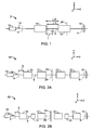
- FIG. 1 is a schematic diagram of an embodiment of an optical lens system 2 for directing radiation from a source 18 to an article 16.
- Optical lens system 2 includes a first lens group 10 and a second lens group 12, each positioned along an optical axis 8 of optical lens system 2.
- Source 18 provides source radiation 14 propagating along optical axis 8 from source plane 4 to output plane 6, passing first through first lens group 10, and then through second lens group 12.
- Article 16 can be positioned in or near output plane 6 to receive the radiation.
- Output plane 6 can be a focal plane of optical lens system 2.
- output plane 6 can be an image plane of optical lens system 2, or another type of plane with respect to optical lens system 2.
- optical lens system 2 can form a portion of a microlithography optical lens system (e.g., a portion of a microlithography optical projection lens system), where source plane 4 is an object plane of the microlithography optical lens system and output plane 6 is an image plane of the microlithography optical lens system.
- Article 16, positioned in or near output plane 6, can be a substrate such as a wafer.
- Optical lens system 2 can also include an element 24 such as an aperture stop for defining an aperture of the microlithography optical lens system.
- Element 24 can be positioned at a location along optical axis 8 to define an aperture.
- element 24 can be positioned within second lens group 12.
- element 24 can be positioned adjacent to output plane 6.
- optical lens system 2 can also include an aperture (not shown) such as an adjustable mask or diaphragm for defining an illumination aperture of the microlithography optical lens system.
- an aperture can be used to provide dipole illumination, quadrupole illumination, annular illumination, or another type of illumination to the microlithography optical lens system.
- Source radiation 14 provided by source 18 includes a distribution of radiation wavelength components.
- the distribution has a central wavelength ⁇ and a full-width at half maximum spectral bandwidth ⁇ .
- Chromatic aberration arises in optical systems due to dispersion in optical components (e.g., a variation of a refractive index in each component with ⁇ ).
- Chromatic aberration can be described in terms of positions of a focus along optical axis 8 of three wavelength components within the spectral bandwidth ⁇ of source radiation 14. Such chromatic aberration is also referred to as longitudinal chromatic aberration, in contrast to horizontal chromatic aberration which refers to variations in the position of focus of different wavelengths in a direction perpendicular to the optical axis.
- the three wavelength components have wavelengths ⁇ 1 , ⁇ 2 , and ⁇ 3 , so that ⁇ 1 ⁇ ⁇ 2 ⁇ ⁇ 3.
- source radiation can include radiation having wavelengths in the visible and near-UV regions of the electromagnetic spectrum, and the wavelengths ⁇ 1 , ⁇ 2 , and ⁇ 3 can correspond to the i, h, and g spectral lines in the emission spectrum of atomic mercury.
- the mercury spectral i-line has a wavelength of 365.01 nm
- the h-line has a wavelength of 404.65 nm
- the g-line has a wavelength of 435.84 nm.
- a magnitude of chromatic aberration refers to a maximum length of a focal region along optical axis 8 in which the wavelength components in source radiation 14 are focused.
- the wavelength components in source radiation 14 which span a spectral bandwidth ⁇ , are focused to different positions along optical axis 8 due to wavelength-dependent dispersion of the various lens materials.
- one component will be focused by an optical lens system to a position along optical axis 8 that is nearer to the lens system than the focal position of any other wavelength component.
- Another wavelength component will be focused by the optical lens system to a position along optical axis 8 that is further away from the lens system than the focal position of any other wavelength component.
- the distance along optical axis 8 between the nearest and furthest focal positions of wavelength components of source radiation 14 is the magnitude of chromatic aberration of the optical lens system for source radiation 14.
- the position of focus of central wavelength ⁇ of source radiation 14 along optical axis 8 defines the position of output plane 6, which lies within the focal region.
- a sign of chromatic aberration refers to a relative ordering of the wavelength components ⁇ 1 , and ⁇ 3 along optical axis 8 and within a focal region of a lens system.
- normal optical dispersion in lens materials causes shorter wavelength optical radiation components to focus at positions closer to the lens system along optical axis 8 than longer wavelength optical radiation components.
- Chromatic aberration that leads to radiation having a wavelength ⁇ 1 focusing to a position along optical axis 8 that is nearer to the lens system than the focal position of radiation having a wavelength ⁇ 3 along optical axis 8 is referred to as positive chromatic aberration.
- Negative chromatic aberration causes radiation having a wavelength ⁇ 3 to focus to a position along optical axis 8 that is nearer to the lens system than the focal position of radiation having a wavelength ⁇ 1 along optical axis 8.
- a first type of chromatic aberration is primary chromatic aberration, which refers to a difference in focal positions along optical axis 108 between optical radiation components having wavelengths ⁇ 1 and ⁇ 3 .
- Optical lens system 2 can be configured to correct for primary chromatic aberration by selectively adjusting the contributions to primary chromatic aberration from first lens group 10 and second lens group 12.
- optical radiation components having wavelengths ⁇ 1 and ⁇ 3 are focused to a common position along optical axis 8 by optical lens system 2.
- a second type of chromatic aberration is secondary chromatic aberration, which refers to a difference in focal positions along optical axis 108 between the common focus of wavelengths ⁇ 1 and ⁇ 3 , and optical radiation having a wavelength ⁇ 2 .
- Secondary chromatic aberration can also be compensated by optical lens system 2 through suitable choice of materials, distances, and lens dimensions.
- optical lens system 2 When secondary chromatic aberration is perfectly compensated, optical radiation components having wavelengths ⁇ 1 , ⁇ 2 , and ⁇ 3 are focused to a common position along optical axis 8 by optical lens system 2.
- optical lens system 2 can be configured to correct for these higher order aberrations.
- optical lens system 2 can correct for tertiary chromatic aberration.
- chromatic aberration of a lens system includes primary chromatic aberration, secondary chromatic aberration, and higher-order chromatic aberrations (e.g., tertiary chromatic aberration).
- First lens group 10 and second lens group 12 are configured to provide a selected chromatic aberration of optical lens system 2 with respect to output plane 6.
- First lens group 10 includes one or more lenses. Each individual lens in first lens group 10 produces chromatic aberration. Dimensions, spacings, and materials for the lenses in first lens group 10 are selected to produce a particular magnitude of a first chromatic aberration for first lens group 10.
- Second lens group 12 includes two or more lenses configured to produce a particular magnitude of a second chromatic aberration for second lens group 12. In certain embodiments, dimensions, spacings, and materials for the lenses in second lens group 12 are selected so that a difference between the magnitudes of the first and second chromatic aberrations is less than a wavelength (e.g., less than ⁇ ) of source radiation 14. Further, second lens group 12 is configured so that the second chromatic aberration has a sign that is opposite to a sign of the first chromatic aberration. That is, the second chromatic aberration can be selected to compensate for the first chromatic aberration.
- the magnitude of the total chromatic aberration can be selected so that each of the optical radiation components having wavelengths ⁇ 1 , ⁇ 2 , and ⁇ 3 is focused substantially to a common focal plane, e.g., output plane 6.
- a common focal plane e.g., output plane 6.
- only paraxial rays having wavelengths ⁇ 1 , ⁇ 2 , and ⁇ 3 can be focused to a common focal plane.
- the magnitude of the chromatic aberration of optical lens system 2 can vary according to the distance d between first lens group 10 and second lens group 12 along optical axis 8.
- Distance d can be chosen to produce a particular magnitude of the chromatic aberration of optical lens system 2 with respect to output plane 6.
- d can be chosen so that a magnitude of a the chromatic aberration of optical lens system 2 with respect to output plane 6 is less than about a wavelength of source radiation 14.
- d can be about five centimeters or more (e.g., about 10 centimeters or more, about 15 centimeters or more, about 20 centimeters or more).
- first lens group 10 can have a variety of configurations and can include various lenses.
- first lens group 10 can include two or more lenses, such as three lenses, or four lenses, or five lenses, or more than five lenses.
- first lens group 10 can include only one lens.
- Each of the lenses can have concave surfaces, convex surfaces, or both concave and convex surfaces.
- Second lens group 12 can also have a variety of configurations and can include various lenses.
- second lens group 12 includes two or more lenses, e.g., three lenses, four lenses, five lenses, or more than five lenses.
- Each of the lenses can have concave surfaces, convex surfaces, or both concave and convex surfaces.
- a maximum diameter of the lenses in the first lens group is at least about 1.5 times greater than a maximum diameter of the lenses in the second lens group.
- the maximum diameter of the lenses in the first lens group can be at least about two times (e.g., at least about three times, at least about four times) greater than a maximum diameter of the lenses in the second lens group.
- the maximum diameter of the lenses in the first lens group can be selected, for example, to allow optical lens system 2 to accommodate large diameter optical fields provided by source 18.
- a distance between a principal plane of first lens group 10 and the first lens of second lens group 12, measured along optical axis 8, is larger than a focal length of the first lens group.
- Principal planes are described, for example, in Michael J. Kidger, "Fundamental Optical Design", Chapter 2, SPIE Press, 2002 .
- a principal plane of first lens group 10 can be determined as follows: a paraxial optical ray from source plane 4, propagating parallel to optical axis 8, enters first lens group 10.
- First lens group 10 focuses the optical ray, so that it emerges from first lens group 10 at an angle to optical axis 8. The ray is focused to a point on optical axis 8. By projecting the focused optical ray backward and the source optical ray forward, a point of intersection between the rays is determined.
- a plane extending through the point of intersection perpendicular to optical axis 8 is a principal plane of the optical system.
- a principal plane 30 of first lens group 10 is shown in FIG. 1 .
- a distance p between principal plane 30 and a first lens of second lens group 12 is larger than a focal length f of first lens group 10.
- p can be at least about 5% larger than f (e.g., at least about 10% larger than f, at least about 20% larger than f, at least about 40% larger than f, at least about 60% larger than f, at least about 80% larger than f).
- a surface of a lens in first lens group 10 that is nearest to source plane 4 (measured along optical axis 8) and that faces source plane 4 can be a concave surface.
- the concave surface can have a radius of curvature that is less than 130 mm, e.g., less than 120 mm, less than 110 mm, less than 100 mm, less than 90 mm, less than 70 mm, less than 50 mm.
- the surface of the lens in first lens group 10 that is nearest to source plane 4 along optical axis 8 and that faces source plane 4 can be a convex surface.
- a radius of curvature of the concave or convex lens surface can be larger than 130 mm, for example.
- a surface of a lens in first lens group 10 that is nearest to element 24 (measured along optical axis 8) and that faces element 24 can be a concave surface.
- the concave surface can have a radius of curvature that is less than 130 mm, e.g., less than 120 mm, less than 110 mm, less than 100 mm, less than 90 mm, less than 70 mm, less than 50 mm.
- the surface of the lens in first lens group 10 that is nearest to element 24 along optical axis 8 and that faces element 24 can be a convex surface.
- a radius of curvature of the concave or convex lens surface can be larger than 130 mm, for example.
- first lens group 10 can be divided into a first lens subgroup having a negative optical power and a second lens subgroup having a positive optical power.
- Each of the first and second lens subgroups can include one or more lenses, for example.
- the first lens subgroup can be positioned optically upstream from the second lens subgroup, that is, the first lens subgroup can be positioned between source plane 4 and the second lens subgroup.
- Source radiation 14 can have spatial intensity modulations in one or more directions transverse to optical axis 8.
- the spatial intensity modulations can define a source pattern.
- the source pattern can be an image of a microlithography mask or reticle.
- optical lens system 2 can be configured to transfer the source pattern from source plane 4 to output plane 6, forming an image of the source pattern in output plane 6.
- the image can be used to expose a substrate, for example.
- lenses focus radiation from source plane 4 to an output surface rather than to an output plane.
- the output surface is, in general, a curved surface having a radius of curvature that is determined by the dimensions, materials, and arrangement of the lenses.
- optical lens system 2 is configured to transfer a source pattern from source plane 4 to form an image of the source pattern in output plane 6, the image of the source pattern can be formed in a curved output surface.
- a curvature of the image is defined as a difference between a position of the center of the image in the curved output surface and a position of a point on an edge of the image in the curved output surface, measured in a direction parallel to optical axis 8.
- first lens group 10 can be configured so that the curvature of the image is less than a depth of focus of optical lens system 2, where the depth of focus is a distance, measured in a direction parallel to optical axis 8, within which the image of the source pattern is in focus.
- a magnification factor M of optical lens system 2 is defined as a ratio of a dimension, in a plane transverse to optical axis 8, of a source pattern in source plane 4 to a corresponding dimension of an image of the source pattern in output plane 6.
- M can be one.
- M can be greater than one.
- M can be at least about two (e.g., at least about three, at least about four, at least about five, at least about ten).
- optical lens systems 2 with M larger than one are reduction optical lens systems, e.g., the image of the source pattern in output plane 6 is smaller than the source pattern in source plane 4.
- optical lens system 2 can be telecentric. That is, optical lens system 2 can be configured so that translating first and second lens groups 10 and 12 along optical axis 8 with respect to source plane 4 produces an image of source radiation 14 in output plane 6, where the magnification factor M of optical lens system 2 is substantially unchanged as the distance between first lens group 10 and source plane 4 is varied. By translating first and second lens groups 10 and 12 along optical axis 8 with respect to source plane 4, the position of output plane 6 with respect to source plane 4 can be selected without significantly changing the magnification factor M of optical lens system 2.
- optical lens system 2 can include a manipulator (not shown) to adjust the magnification factor M of the system.
- the manipulator can be an actuator (e.g., an electromechanical actuator such as a piezoelectric actuator, a motor having a rotating shaft which moves in an axial direction, or another type of actuator) coupled to one or more movable components that can be used to adjust positions of various lenses in optical lens system 2.
- the manipulator can include a lens mount configured to support one or more lenses, and attached to a movable stage.
- the lens mount can be positioned to support one or more lenses of first lens group 10 or second lens group 12.
- the lens mount can be translated along the direction of optical axis 8 either manually or in automated fashion.
- the movable stage can be translated by a motor controlled by a computer.
- Computer control of the movable stage can be passive (e.g., during construction of optical lens system 2) and/or active (e.g., during operation of optical lens system 2).
- the dimensions, materials, and arrangement of lenses in first lens group 10 and in second lens group 12 can be selected to provide a particular numerical aperture for optical lens system 2.
- a numerical aperture of optical lens system 2 can be at least about 0.1 (e.g., at least about 0.15, at least about 0.2, at least about 0.25, at least about 0.5) in output plane 6.
- a field size of source radiation 14 is defined as a full-width at half maximum of an intensity distribution of source radiation 14 in output plane 6, measured along a direction in a plane transverse to optical axis 8.
- a maximum field size can be about 10 millimeters or more.
- the maximum field size can be about 20 millimeters or more (e.g., about 30 millimeters or more, about 50 millimeters or more, about 80 millimeters or more, about 90 millimeters or more, about 100 millimeters or more, about 120 millimeters or more).
- source radiation 14 has an intensity distribution in a plane transverse to optical axis 8 that is substantially circular.
- the transverse intensity distribution of source radiation 14 has a non-circular shape such as an ellipse, for example.
- a length L of optical lens system 2 is defined as a maximum distance along optical axis 8 between any two lenses in optical lens system 2.
- L can be about 10 meters or less (e.g., about five meters or less, about four meters or less, about three meters or less, about two meters or less, about one meter or less).
- the length L is about 20 times or less the maximum field size of source radiation 14.
- L can be about 16 times or less (e.g., about 14 times or less, about 12 times or less, about 10 times or less, about 8 times or less, about 6 times or less) the maximum field size of source radiation 14.
- Lenses in optical lens system 2 can have spherical or aspherical surfaces.
- the aspherical surfaces may have dimensions that are selected to eliminate or reduce certain imaging aberrations relative to optical lens systems that have only spherical lens surfaces.
- optical lens system 2 can include at least one lens that has an aspherical surface.
- optical lens system 2 can include at least two lenses, each of which has at least one aspherical surface.
- at least one of the lenses in first lens group 10 can have an aspherical surface
- at least one of the lenses in second lens group 12 can have an aspherical surface.
- P(h) is a distance of the aspherical surface from a plane perpendicular to the optical axis as a function of a perpendicular distance h from the optical axis
- R is a radius of curvature of the lens at its apex.
- the parameter CC is the conic constant of the aspheric surface, and parameters C 1 to C n are aspheric constants.
- source 18 can be configured to provide broadband source radiation 14.
- source radiation 14 can have a distribution of wavelengths of electromagnetic radiation with a spectral bandwidth ⁇ of about 0.5 nanometer or more (e.g., about five nanometers or more, about 10 nanometers or more, about 25 nanometers or more, about 50 nanometers or more, about 70 nanometers or more).
- source 14 can include one or more optical filter elements to select particular central wavelengths and/or bandwidths for source radiation 14. Filter elements can include interference filters, optical modulators such as liquid crystal modulators, and other elements that perform spectral filtering functions.
- source radiation 14 can have at least one wavelength in the visible region of the electromagnetic spectrum.
- source radiation 14 can have at least one wavelength in the ultraviolet region of the electromagnetic spectrum.
- a central wavelength ⁇ of source radiation 14 can be in the ultraviolet region of the electromagnetic spectrum, but source radiation 14 can also include one or more wavelengths in the visible region of the electromagnetic spectrum.
- a central wavelength ⁇ of source radiation 14 can be in the visible region of the electromagnetic spectrum, but source radiation 14 can also include one or more wavelengths in the ultraviolet region of the electromagnetic spectrum.
- the central wavelength ⁇ of source radiation 14 can be about 450 nm or less (e.g., about 400 nm or less, about 350 nm or less, about 300 nm or less, about 300 nm or less, about 250 nm or less, about 200 nm or less).
- source radiation 14 includes significant power at two or more (e.g., three, four, five or more) discrete wavelengths.
- source radiation 14 can include significant power at two or more wavelengths corresponding to emission lines of source 18.
- source radiation 14 can include significant power at the i-, h-, and g-emission lines of a mercury source.
- Source 18 provides source radiation 14.
- source 18 can be a mercury vapor lamp, for example.
- source 18 can include light emitting diodes (LEDs).
- the diodes can all have a similar light emission spectrum or, alternatively, some or all of the diodes can have different emission spectra.
- the spectra can be complementary, so that the total spectral bandwidth ⁇ of source radiation 14 can be larger than an emission bandwidth of any of the individual diodes.
- source 18 can include a laser system, such as a broadband laser system, for producing source radiation 14 with a suitable spectral bandwidth.
- optical lens systems includes more than two lens groups.
- FIG. 2A is a schematic diagram of an embodiment of an imaging optical lens system 50 that is configured as a imaging optical lens system.
- Optical lens system 50 is configured to transfer source radiation 14 emerging from spatial locations in source plane 4 to corresponding spatial locations in output plane 6.
- optical lens system 50 can be configured as a telecentric imaging system (e.g., a double telecentric imaging system), so that a distance g between source plane 4 and first lens group 10 can be varied without changing a magnification factor M of optical lens system 50.
- optical lens system 50 also includes third lens group 20 and fourth lens group 22.
- third lens group 20 and fourth lens group 22 can include one or more lenses positioned along optical axis 8.
- the properties and features of third lens group 20 can be similar to the properties and features described above in connection with second lens group 12.
- the properties and features of fourth lens group 22 can be similar to the properties and features described above in connection with first lens group 10.
- optical lens system 50 can be a symmetric lens system, where first, second, third, and fourth lens groups 10, 12, 20, and 22 are symmetrically positioned about symmetry plane 26, which is perpendicular to optical axis 8.
- each lens in second lens group 12 has a similar corresponding lens in third lens group 20, and the lenses in the second and third lens groups 12 and 20 are symmetrically arranged along optical axis 8 with respect to symmetry plane 26.
- each lens in first lens group 10 has a similar corresponding lens in fourth lens group 22, and the lenses in the first and fourth lens groups 10 and 22 are symmetrically arranged along optical axis 8 with respect to symmetry plane 26.
- Similar lenses have the same design and are formed from the same material.
- an optical lens system 60 is an imaging optical lens system that includes six lens groups, indicated as lens groups 10, 13, 12, 20, 23, and 22.
- Optical lens system 60 is be symmetric with respect to plane 26.
- symmetry plane 26 corresponds to a pupil plane of optical lens system 60.
- lens groups 10, 12, 20, and 22 are all positive lens groups.
- Lens group 10 helps to form an image of the entrance pupil, while lens group 12 helps to form an image of an object positioned at source plane 4.
- Lens groups 13 and 23 are negative lens groups, also arranged symmetrically with respect to plane 26.
- lens groups 10, 12, 13, 20, 22, and 23 can each include one or more lenses.
- lens group 10 is includes a first lens subgroup (e.g., one or more lenses) having positive optical power and a second lens subgroup (e.g., one or more lenses) having negative optical power.
- the first and second lens subgroups can be designed as a retrofocus system, with the negative lens subgroup being position between source plane 4 and the positive lens subgroup. It is believed that such an arrangement can reduce image curvature of the optical lens system relative to other arrangements.
- lens group 22 also includes a positive and negative lens subgroup arranged symmetrically relative to the first and second lens subgroups of lens group 10.
- lens groups 10 and 22 can include a third lens subgroup (e.g., one or more lenses) in addition to the first and second lens subgroups.
- the third lens subgroups can have positive optical power and, in lens group 10, the third lens subgroup can be positioned between the negative lens subgroup and source plane 4.
- the third lens subgroup in lens group 22 can be positioned between the negative lens subgroup and output plane 6. It is believed that a third lens subgroup having positive optical power can help reduce telecentricity errors and other field-dependent aberrations without the use of aspheric surfaces.
- chromatic aberration e.g., primary and/or secondary chromatic aberration
- optical lens system 60 can be reduced by providing only weak correction of chromatic aberration in portions of the optical lens system where the marginal rays are located relatively far from optical axis 8.
- the marginal rays have their maximum distance from optical axis 8 (measured perpendicularly from optical axis 8) in the region of lens groups 12 and 20.
- lens groups 12 and 20 can be designed so that these groups provide only weak correction (or overcorrection) of chromatic aberration.
- lens groups 12 and 20 include at least on positive-negative lens doublet (PN doublet) in which the positive lens displays relative weak dispersion while the negative lens displays relatively strong dispersion.
- PN doublet positive-negative lens doublet
- lens groups 12 and 20 can each include more than one (e.g., two, three, four, more than four) positive-negative lens doublet.
- a negative lens in one of the positive-negative lens doublets in lens groups 12 and 20 can be positioned closest to symmetry plane 26 on the respective sides of symmetry plane 26. It is believed that improved reduction in chromatic aberration can be achieved using such an arrangement. Furthermore, it is believed that such an arrangement can contribute to leveling the pupil image in optical lens system 60, which can result in improved preservation of the symmetry of all ray bundles in the system.
- lenses in optical lens systems 2, 50, and 60 are formed of materials that are selected based on criteria such as a material's dispersion, absorption properties, mechanical properties, chemical properties (e.g., purity), and on other criteria, such as commercial availability.
- Different lenses in the optical lens systems can be formed from different materials. For example, in embodiments, two or more different lens materials are used in order to reduce chromatic aberration.
- Lens materials can be characterized in terms of their refractive index at a particular wavelength. Typically, a lens material has a refractive index in a range from about 1.4 to about 1.7, although certain materials have a refractve index higher than 1.7. Lens materials can also be characterized in terms of an Abbé number, V, which provides a characterization of the materials dispersion over a range of wavelengths.
- a lower Abbé number is indicative of a material with relatively strong dispersion and a higher Abbé number is indicative of a material with a relatively weak dispersion.
- lens materials suitable for use with radiation in the UV can be categorized in three different groups based on their Abbé numbers and refractive indexes.
- a first group, designated group A includes materials that have an Abbé number, Vi, in a range from 40 to 70, inclusive.
- the materials in group A have a refractive index in a range from 1.46 to 1.56.
- Materials in group A can include crown glasses, such fused silica (SiO 2 ) and borosilicate glasses (e.g., BK7 glass). Other examples include K5 glass, K7 glass, and FK5 glass.
- a second group, designated group B, includes materials that have an Abbé number greater than 70.
- the materials in group B have a refractive index less than about 1.46.
- CaF 2 is an example of a material in group B.
- a third group, designated group C includes materials that have an Abbé number less than 40.
- the materials in group C have a refractive index greater than about 1.56.
- Materials in group C can include flint glasses, such as LLF-6 glass, LLF-1 glass, or LF-5 glass.
- an optical lens system should included lenses formed from at least two materials having different dispersions. Accordingly, embodiments are disclosed below that include at least one lens from two different groups shown in FIG. 3 . Furthermore, it is believed that further reduction can be achieved using lenses formed from at least three materials having different dispersions. Accordingly, embodiments are disclosed below that include lenses formed from three different materials. For example, embodiments can include at least one lens formed from a material in group A, at least one lens formed from a material in group B, and at least one lens formed from a material in group C.
- optical lens system 2 in some embodiments, some of the lenses in lens group 10 and/or in lens group 12 in optical lens system 2 can be made from a silica material such as UV-grade fused silica. Some of the lenses in first lens group 10 and/or in second lens group 12 can be made from a material in group C.
- embodiments of optical lens system 2 can include at least one lens formed of a material in group B and at least one lens formed form a material in group A.
- optical lens system 2 can include at least one lens formed of fused silica and at least one lens formed of LLF-1 glass.
- lens group 10 can include two lenses formed of different materials and having different dispersions with respect to a wavelength of source radiation 14.
- at least one of the lenses in lens group 10 can be a lens formed of a material in group A (e.g., fused silica), and at least one other of the lenses in first lens group 10 can be a lens formed of a material in group C (e.g., LLF-1 glass).
- the lens formed form the material in group C can be positioned neared source plane 4.
- lens group 12 can include two lenses formed of different materials and having different dispersions with respect to a wavelength of source radiation 14.
- at least one of the lenses in second lens group 12 can be a lens formed of a material in group A (e.g., fused silica), and at least one other of the lenses in second lens group 12 can be a lens formed of a material in group C (e.g., LLF-1 glass).
- second lens group 12 can include at least one doublet of lenses, where a first lens of the doublet has a positive optical power and a second lens of the doublet has negative optical power.
- the positive lens can be formed of a material having relatively weak dispersion, such as a material in group A (e.g., BK7) or group B (e.g., CaF 2 ), while the negative lens is formed from a material having relatively strong dispersion, such as a material in group C (e.g., LLF-1 glass).
- group A e.g., BK7
- group B e.g., CaF 2
- group C e.g., LLF-1 glass
- materials used for lenses can have very low optical absorption for wavelengths in source radiation 14. Absorption of radiation by lens materials can lead to thermal expansion of the lenses, producing changes in an index of refraction of the lens materials and changes in the shape of the lenses.
- lens materials such as silica and CaF 2 that absorb weakly the wavelengths in source radiation 14
- effects due to thermal expansion of the lenses can be reduced.
- Materials such as silica and CaF 2 produce less secondary chromatic aberration than materials such as LLF-1 glass. Accordingly, in optical lens system 2, for example, the spacing d between first lens group 10 and second lens group 12 can be reduced relative to lens systems that include more secondary chromatic aberration.
- optical lens systems 2, 50, or 60 can be configured so that a magnitude of chromatic aberration is about a wavelength or less of source radiation 14 using lenses formed from only two different materials.
- the optical lens systems can include at least one lens formed from a material from group A (e.g., fused silica) and at least one lens formed from a material from group C (e.g., LLF-1 glass).
- optical lens systems 2, 50, or 60 can be configured so that a magnitude of chromatic aberration is about a wavelength or less of source radiation 14 using lenses formed from only three different materials.
- the optical lens systems can include at least one lens formed from a material from group A (e.g., fused silica), at least one lens formed from a material from group B (e.g., CaF 2 ) and C at least one lens formed from a material from group C (e.g., LLF-1 glass).
- optical lens systems 2, 50, and 60 each include multiple lens groups, and each of the multiple lens groups can include one or multiple lenses.
- the lens groups can be configured to reduce a curvature of an image formed by the optical lens system to less than a depth of focus of the optical lens system.
- the dimensions and/or properties and/or materials and/or features disclosed in connection with first and second lens groups 10 and 12 can, in general, be shared by other lens groups and lenses thereof, as appropriate.
- optical lens systems can be configured so that relatively few lenses are positioned at locations where the cross-sectional intensity distribution of the radiation is substantially inhomogeneous.
- One way to characterize the cross-sectional intensity distribution of the radiation on a lens surface is from the ratio of the sub-aperture, SA , to the clear aperture, CA , of the radiation at each lens surface.
- the clear aperture, CA at a lens surface refers to the area of the lens illuminated from all field points at the object region.
- the sub-aperture, SA at a lens surface refers to the maxiumum area of the lens illuminated from a single field point at the object region.
- the ratio SA / CA at lens position z can be approximated by: SA CA z ⁇ RS z RS z + HS z
- HS ( z ) denotes the height of the marginal ray at position z
- RS ( z ) is the difference between HS ( z ) and the height of the chief ray of the uppermost field point at position z (see, e.g., 'Fundamental Optical Design', by M.J. Kidger, p.7). All quantities are defined in the meridian plane.
- d max is given as l 2 2 + w 2 2 .
- Non-rectangular fields are also contemplated.
- d max corresponds to the circle radius.
- d max corresponds to the radius along the semi-major axis.
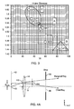
- the analysis disclosed herein can be applied to an arbitrary field size and shape. Further, note that in FIG. 4A , stop 45 is positioned at pupil plane 46 and object 43 is positioned at object region 42.
- the lens is placed in the vicinity of the object region.
- the SA / CA ratio is one the lens is positioned in the pupil plane.
- An optical lens system can be characterized by averaged parameters related to the values of
- the ⁇ ratio provides a measure of the geometrical distribution of lenses within the optical lens system and therefore also a measure of the expected homogeneity of the intensity distribution onto the lenses.
- an optical lens system can be considered to include three different zones between the object region and the pupil plane. These are shown as region A, B, and C in FIG. 4B .
- the optical lens system includes regions C', B', and A' between the pupil plane and the image region.
- Regions A and A' are regions in which lenses have a relatively small
- Regions C and C' are regions in which lenses have relatively large
- Regions B and B' are regions in which lenses have intermediate
- optical lens systems can include relatively few lenses positioned between the object region and the pupil plane that have a surface with a
- optical lens systems can include two or fewer (e.g., one or zero) lenses positioned between the object region and the pupil plane that have a surface with a
- a relatively small number of lenses in the optical lens system can include surfaces that contribute to M b .
- a relatively small number of lenses positioned between the object region and the pupil plane have a
- optical lens systems can include no more than four (e.g., three or fewer, two or fewer) lenses that include surfaces that contribute to M b .
- 40% or fewer (e.g., 35% or fewer, 30% or fewer, 25% or fewer, 20% or fewer) of the total number of lenses positioned between the object region and the pupil plane include surfaces that contribute to M b .
- embodiments with relatively few lenses positioned at locations where the cross-sectional intensity distribution of the radiation is substantially inhomogeneous can exhibit reduced wavefront aberrations due to variations in the lenses due to heating by the radiation.
- such optical lens systems can exhibit reduced variations in distortion, astigmatism, and/or coma over a range of input powers relative to other systems where the distribution of lenses along the optical axis relative to the image and object regions and pupil plane is different.
- the lenses tend to be positioned either close to the object region and/or close to the pupil plane.
- the intensity distribution on the lenses will be relatively homogeneous and, in turn, lens heating effects will be relatively small.
- ⁇ is large (e.g., where M a is relatively large, such as about 0.31 or more, and/or M b is relatively small, such as about 0.85 or less), a larger proportion of lenses tend to be positioned in intermediate zone B, midway between the object region and the pupil plane where the illumination is relatively inhomogeneous across the lens surfaces.
- the effect of lens heating on the imaging properties of an optical lens system can be relatively large.
- optical lens systems can have a ⁇ ratio of less than 0.33 (e.g., 0.32 or less, 0.31 or less, 0.30 or less, 0.29 or less, 0.28 or less, 0.27 or less, 0.26 or less, 0.25 or less).
- Optical lens systems having a ⁇ ratio of less than 0.33 can have good lens heating properties.
- variations in imaging aberrations in optical lens systems with ⁇ ratios less than 0.33 can be relatively small over a range of input powers.
- the optical lens system has an NA max of 0.2
- a ⁇ ratio of less than 0.33 can correspond to good lens heating properties.
- a ⁇ ratio of less than 0.28 can correspond to good lens heating properties.
- the heating properties of an optical lens system depends on the size of the field.
- lenses in an optical lens system having a large field size should be arranged to have a relatively small ⁇ value compared to a similar lens with a smaller field size to provide a system with good heating properties.
- Table 1 exemplary ranges of ⁇ ratio are provided for optical lens systems with differing field sizes (given by d max ) and differing NA max . These ⁇ ratios can correspond to optical lens systems with good heating properties. For example, in embodiments where the lenses are arranged symmetrically with respect to the pupil plane and the optical lens systems have a magnification of one, these ranges of ⁇ ratios for corresponding NA max values and field sizes can provide good heating properties.
- the effect of lens heating on the imaging properties in an optical lens system can be characterized in a variety of ways.
- the effects can be characterized by the variation of imaging aberrations as a function of radiation power input into the optical lens system at wavelength ⁇ .
- An example of this is the variation in astigmatism over a range of input powers. This refers to the variation with input power in a distance between the focal position of a line extending along the x-direction intersecting the optical axis, and a line extending along the y-direction intersecting the optical axis.
- optical lens systems can have a maximum astigmatism variation of 400 nm/W or less (e.g., 300 nm/W or less, 250 nm/W or less, 200 nm/W or less,175 nm/W or less, 160 nm/W or less, 150 nm/W or less, 140 nm/W or less) at the image region for an input radiation power at the operational wavelength(s) up to 40 W.
- nm/W or less e.g., 300 nm/W or less, 250 nm/W or less, 200 nm/W or less,175 nm/W or less, 160 nm/W or less, 150 nm/W or less, 140 nm/W or less
- optical lens systems can have a peak-to-valley focal plane deviation variation of 700 nm/W or less (e.g., 500 nm/W or less, 400 nm/W or less, 300 nm/W or less, 290 nm/W or less, 280 nm/W or less, 270 nm/W or less, 260 nm/W or less) at the image region for an input radiation power at the operational wavelength(s) up to 40 W.
- nm/W or less e.g., 500 nm/W or less, 400 nm/W or less, 300 nm/W or less, 290 nm/W or less, 280 nm/W or less, 270 nm/W or less, 260 nm/W or less
- optical lens systems can have a peak-to-valley field curvature variation of 600 nm/W or less (e.g., 500 nm/W or less, 400 nm/W or less, 300 nm/W or less, 280 nm/W or less, 260 nm/W or less, 250 nm/W or less, 240 nm/W or less, 230 nm/W or less) at the image region for an input radiation power at the operational wavelength(s) up to 40 W.
- 600 nm/W or less e.g., 500 nm/W or less, 400 nm/W or less, 300 nm/W or less, 280 nm/W or less, 260 nm/W or less, 250 nm/W or less, 240 nm/W or less, 230 nm/W or less
- Lens heating effects can also be characterized by variations in on-axis astigmatism of an optical lens system.
- On-axis astigmatism refers to a distance between the focal position of a line extending along the x-direction intersecting the optical axis, and a line extending along the y-direction intersecting the optical axis, where the distance is measured on-axis.
- optical lens systems have a maximum on-axis astigmatism variation of-120 nm/W or less (e.g, -100 nm/W or less, -80 nm/W or less, -70 nm/W or less, -60 nm/W or less,-55 nm/W or less, -52 nm/W or less, -50 nm/W or less, -48 nm/W or less, -45 nm/W or less) at the image region for an input radiation power at the operational wavelength(s) up to 40 W.
- the term "maximum” refers to the absolute value of the variation.
- a further parameter that can provide information about how effects of lens heating affect the imaging properties of an optical lens system is variation in maximum distortion.
- Distortion refers to the variation in relative displacement of field points at the object and image regions.
- optical lens systems have a maximum distortion variation of 12 nm/W or less (e.g., 10 nm/W or less, 9 nm/W or less, 8 nm/W or less, 7 nm/W or less, 6 nm/W or less, 5 nm/W or less, 4 nm/W or less) at the image region for an input radiation power at the operational wavelength(s) up to 40 W.
- ray tracing software e.g., commercially-available ray tracing software such as Code V from ORA, Pasadena, CA
- ray tracing software such as Code V from ORA, Pasadena, CA
- a finite element analysis can be used to solve the heat transport equation for each lens and calculate heat induced changes in the lens, such as a change of refractive index and/or a surface deformation.
- the heat induced changes result in a perturbed optical lens system for which additional imaging calculations can be performed.
- ray tracing can be performed for an expected arial image can be simulated for structures of differing orientation at the object region and for different field points in the object region.
- the simulation of the arial image is based on two-beam interference accounting for the problem of partial coherence and takes the optical transfer function of the system into account. Using the simulated arial image, one can determine a best focus for the system, as well as a pattern shift in the x- and y- directions for the different structures.
- Aberrations such as astigmatism, focal plane deviation, and other parameters, can be calculated to provide the information characterizing the heating of the optical lens system.
- Optical lens systems 2, 50 and 60 can be used in microlithography systems.
- optical lens system 2, 50, and/or optical lens system 60 can form a portion of a microlithography optical projection lens system.
- Optical lens systems 2, 50, and 60 can be configured so that output plane 6 of the optical lens system coincides with an image plane of the microlithography system.
- an article 16 such as a substrate can be positioned in or near output plane 6, and source radiation 14 can be directed through optical lens system 2 and/or 50 to expose the substrate to the radiation.
- an exemplary microlithography system 70 includes a source 71, an illumination system 72, a reticle 76 positioned on a reticle stage 74, an optical lens system 73, and a stage 75, which supports a wafer 77.
- Wafer 77 is positioned at the image region of optical lens system 73.
- Reticle 76 is positioned at the object region of optical lens system 73.
- a layer of a resist (a light sensitive material) is disposed on the surface of wafer 77.
- source 71 directs radiation R71 to illumination system 72, which directs the radiation to reticle 76, as indicated by arrow R72.
- Optical lens system 73 projects an image of a pattern on reticle 76 onto the resist layer using the radiation, as indicated by arrow R73.
- Stage 75 moves wafer 77 relative to optical lens system 73, exposing different regions of the resist layer to the radiation.
- Embodiments can be used in so-called "I-line" lithography tools which utilize the i-line of a mercury source.
- the optical lens sytem can be designed to have low chromatic aberration at other wavelengths of the mercury source (e.g., at the g and h lines), allowing radiation at both the i-line and the other wavelengths to be used to expose the substrate.
- the additional wavelengths can provide higher power delivery to the substrate relative to systems which expose the substrate only to i-line radiation, allowing for shorter exposure time and increased throughput.
- microlithography system 70 can have a throughput of about 125 30 mm diameter wafers per hour (WPH) or more (e.g., about 150 WPH or more, about 175 WPH or more, about 200 WPH or more, about 225 WPH or more, about 250 WPH or more).
- WPH wafers per hour
- multiple substrates can be exposed to source radiation 14.
- the multiple substrates can be multiple dies, and a field size of source radiation 14 can be sufficiently large so that multiple dies can be simultaneously exposed to the radiation.
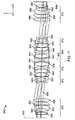
- optical lens systems having different properties such as different numerical apertures in output plane 6 and different lens materials.
- Each of these optical lens systems can be used in microlithography systems.
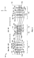
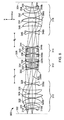
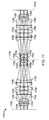
- Optical lens system 100 is configured to transfer a light pattern from object plane 102 to image plane 104 through symmetry plane 106.
- Optical lens system 100 includes a first lens group 110, a second lens group 112, a third lens group 114, and a fourth lens group 116.
- Each of the lenses in the lens groups is rotationally symmetric about axis 108, which is parallel to the z-axis in the coordinate system shown.
- Optical lens system 100 is configured to provide a maximum numerical aperture of 0.20.
- Optical lens system 100 has an M a value of 0.31, an M b value of 0.82, and a ⁇ ratio of 0.38.
- Each of the lenses in optical lens system 100 has a first surface facing object plane 102 and a second surface facing image plane 104.
- the first surface of each lens is denoted with an "a" label.
- the first surface of lens 118 is labeled 118a.
- the second surface of each lens is denoted with a "b" label.
- the second surface of lens 118 is labeled 118b.
- Not all labels corresponding to first and second surfaces of the lenses in FIG. 6 are shown for purposes of clarity, but each lens includes first and second surfaces labeled "a" and "b", respectively.
- First lens group 110 includes lenses 118, 120, 122, 124, 126, and 128.
- Lenses 118, 120, and 126 are formed of fused silica.
- Lenses 122, 124, and 128 are formed of a flint glass material such as LLF-1 glass. Thicknesses of the lenses in optical lens system 100 are measured along axis 108.
- Lens 118 has a thickness of 10.0 mm.
- Lens 120 has a thickness of 10.0 mm.
- Lens 122 has a thickness of 41.1 mm.
- Lens 124 has a thickness of 47.3 mm.
- Lens 126 has a thickness of 10.0 mm.
- Lens 128 has a thickness of 45.2 mm.
- Lens 118 is spaced from lens 120 by a distance of 29.6 mm.
- Lens 120 is spaced from lens 122 by a distance of 3.6 mm.
- Lens 122 is spaced from lens 124 by a distance of 1.0 mm.
- Lens 124 is spaced from lens 126 by a distance of 1.0 mm.
- Lens 126 is spaced from lens 128 by a distance of 1.0 mm.
- First lens group 110 is spaced from second lens group 112 by a distance d 1 measured along axis 108 (e.g., a distance measured between surfaces 128b and 130a along axis 108) of 171.2 mm.
- Second lens group 112 includes lenses 130, 132, 134, and 136.
- Lenses 132 and 136 are formed of fused silica.
- Lenses 130 and 134 are formed of a flint glass such as LLF-1 glass.
- Lens 130 has a thickness of 10.0 mm.
- Lens 132 has a thickness of 33.0 mm.
- Lens 134 has a thickness of 10.0 mm.
- Lens 136 has a thickness of 20.0 mm.
- Lens 130 is spaced from lens 132 by a distance of 1.0 mm. Lenses 132 and 134 are immediately adjacent along axis 108. Lens 134 is spaced from lens 136 by a distance of 1.0 mm. Second lens group 112 is spaced from symmetry plane 106 by a distance (e.g., a distance measured between surface 136b and symmetry plane 106 along axis 108) of 5.8 mm.
- Third lens group 114 includes lenses 138, 140, 142, and 144.
- Lenses 138 and 142 are formed of fused silica.
- Lenses 140 and 144 are formed of a flint glass such as LLF-1 glass.
- Lens 138 has a thickness of 20.0 mm.
- Lens 140 has a thickness of 10.0 mm.
- Lens 142 has a thickness of 33.0 mm.
- Lens 144 has a thickness of 10.0 mm.
- Third lens group 114 is spaced from symmetry plane 106 by a distance (e.g., a distance measured between symmetry plane 106 and surface 138a along axis 108) of 5.8 mm.
- Lens 138 is spaced from lens 140 by a distance of 1.0 mm.
- Lenses 140 and 142 are immediately adjacent along axis 108.
- Lens 142 is spaced from lens 144 by a distance of 1.0 mm.
- Third lens group 114 is spaced from fourth lens group 116 by a distance d 2 measured along axis 108 (e.g., a distance measured between surfaces 144b and 146a along axis 108) of 171.2 mm.
- third lens group 114 The dimensions, spacings, and materials of lenses in third lens group 114 are similar to the dimensions, spacings, and materials of lenses in second lens group 112.
- the lenses in third lens group 114 are positioned along axis 108 so that second lens group 112 and third lens group 114 form an arrangement of lenses that is symmetric with respect to symmetry plane 106.
- Fourth lens group 116 includes lenses 146, 148, 150, 152, 154, and 156.
- Lenses 148, 154, and 156 are formed of fused silica.
- Lenses 146, 150, and 152 are formed of a flint glass such as LLF-1 glass.
- Lens 146 has a thickness of 45.2 mm.
- Lens 148 has a thickness of 10.0 mm.
- Lens 150 has a thickness of 47.3 mm.
- Lens 152 has a thickness of 41.1 mm.
- Lens 154 has a thickness of 10.0 mm.
- Lens 156 has a thickness of 10.0 mm.
- Lens 146 is spaced from lens 148 by a distance of 1.0 mm.
- Lens 148 is spaced from lens 150 by a distance of 1.0 mm.
- Lens 150 is spaced from lens 152 by a distance of 1.0 mm.
- Lens 152 is spaced from lens 154 by a distance of 3.6 mm.
- Lens 154 is spaced from lens 156 by a distance of 29.6 mm.
- Fourth lens group 116 is spaced from image plane 104 by a distance (e.g., a distance measured between surface 156b and image plane 104 along axis 108) of 48.1 mm.
- the dimensions, spacings, and materials of lenses in fourth lens group 116 are similar to the dimensions, spacings, and materials of lenses in first lens group 110.
- the lenses in fourth lens group 116 are positioned along axis 108 so that first lens group 110 and fourth lens group 116 form an arrangement of lenses that is symmetric with respect to symmetry plane 106.
- Lens data including a radius of curvature of each of the surfaces of each of the lenses in optical lens system 100, is shown in Table 2A.
- the radius of curvature of a lens surface is negative if the center of curvature of the lens surface is on the same side of the lens surface as object plane 102.
- the radius of curvature of a lens surface is positive if the center of curvature of the lens surface is on the same side of the lens surface as image plane 104.
- Some of the surfaces of the lenses in optical lens system 100 are aspherical surfaces. Specifically, surfaces 118b, 124a, 126a, 128b, 130a, 136b, 138a, 144b, 146a, 148b, 150b, and 156a are aspherical surfaces.
- the other lens surfaces in optical lens system 100 are spherical surfaces. Aspherical surfaces are identified in Table 2A as having a shape "AS”. Aspheric constants corresponding to Equation 1 for the aspherical surfaces of lenses in optical lens system 100 are shown in Table 2B.
- a principal plane 160 of first lens group 110 is shown in optical lens system 100.
- the principal plane lies between first lens group 110 and second lens group 112.
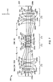
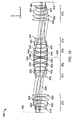
- Optical lens system 200 is configured to transfer a light pattern from object plane 202 to image plane 204 through symmetry plane 206.
- Optical lens system 200 includes a first lens group 210, a second lens group 212, a third lens group 214, and a fourth lens group 216.
- Each of the lenses in the lens groups is positioned symmetrically about axis 208, which is parallel to the z-axis in the coordinate system shown.
- Optical lens system 200 is configured to provide a maximum numerical aperture of 0.16.
- Optical lens system 200 has an M a value of 0.28, an M b value of 0.8, and a ⁇ ratio of 0.35.
- Each of the lenses in optical lens system 200 has a first surface facing object plane 202 and a second surface facing image plane 204.
- the first surface of each lens is denoted with an "a" label.
- the first surface of lens 218 is labeled 218a.
- the second surface of each lens is denoted with a "b" label.
- the second surface of lens 218 is labeled 218b.
- First lens group 210 includes lenses 218, 220, 222, 224, 226, and 228.
- Lenses 218, 220, and 226 are formed of fused silica.
- Lenses 222, 224, and 1228 are formed of a flint glass such as LLF-1 glass. Thicknesses of the lenses in optical lens system 200 are measured along axis 208.
- Lens 218 has a thickness of 10.0 mm.
- Lens 220 has a thickness of 10.0 mm.
- Lens 222 has a thickness of 38.4 mm.
- Lens 224 has a thickness of 43.1 mm.
- Lens 226 has a thickness of 10.0 mm.
- Lens 228 has a thickness of 40.3 mm.
- Lens 218 is spaced from lens 220 by a distance of 27.1 mm.
- Lens 220 is spaced from lens 222 by a distance of 4.0 mm.
- Lens 222 is spaced from lens 224 by a distance of 1.0 mm.
- Lens 224 is spaced from lens 226 by a distance of 1.0 mm.
- Lens 226 is spaced from lens 228 by a distance of 1.0 mm.
- First lens group 210 is spaced from second lens group 212 by a distance d 3 measured along axis 208 (e.g., a distance measured between surfaces 228b and 230a along axis 208) of 178.2 mm.
- Second lens group 212 includes lenses 230, 232, 234, and 236.
- Lenses 232 and 236 are formed of fused silica.
- Lenses 230 and 234 are formed of a flint glass such as LLF-1 glass.
- Lens 230 has a thickness of 10.0 mm.
- Lens 232 has a thickness of 33.0 mm.
- Lens 234 has a thickness of 10.0 mm.
- Lens 236 has a thickness of 20.0 mm.
- Lens 230 is spaced from lens 232 by a distance of 1.0 mm.
- Lenses 232 and 234 are immediately adjacent along axis 208.
- Lens 234 is spaced from lens 236 by a distance of 1.0 mm.
- Second lens group 212 is spaced from symmetry plane 206 by a distance (e.g., a distance measured between surface 236b and symmetry plane 206 along axis 208) of 6.0 mm.
- Third lens group 214 includes lenses 238, 240, 242, and 244.
- Lenses 238 and 242 are formed of fused silica.
- Lenses 240 and 244 are formed of a flint glass such as LLF- I glass.
- Lens 238 has a thickness of 20.0 mm.
- Lens 240 has a thickness of 10.0 mm.
- Lens 242 has a thickness of 33.0 mm.
- Lens 244 has a thickness of 10.0 mm.
- Third lens group 214 is spaced from symmetry plane 206 by a distance (e.g., a distance measured between symmetry plane 206 and surface 238a along axis 208) of 6.0 mm.
- Lens 238 is spaced from lens 240 by a distance of 1.0 mm.
- Lenses 240 and 242 are immediately adjacent along axis 208.
- Lens 242 is spaced from lens 244 by a distance of 1.0 mm.
- Third lens group 214 is spaced from fourth lens group 216 by a distance d 4 measured along axis 208 (e.g., a distance measured between surfaces 244b and 246a along axis 208) of 178.2 mm.
- third lens group 214 The dimensions, spacings, and materials of lenses in third lens group 214 are similar to the dimensions, spacings, and materials of lenses in second lens group 212.
- the lenses in third lens group 214 are positioned along axis 208 so that second lens group 212 and third lens group 214 form an arrangement of lenses that is symmetric with respect to symmetry plane 206.
- Fourth lens group 216 includes lenses 246, 248, 250, 252, 254, and 256.
- Lenses 248, 254, and 256 are formed of fused silica.
- Lenses 246, 250, and 252 are formed of a flint glass such as LLF-1 glass.
- Lens 246 has a thickness of 40.3 mm.
- Lens 248 has a thickness of 10.0 mm.
- Lens 250 has a thickness of 43.1 mm.
- Lens 252 has a thickness of 38.4 mm.
- Lens 254 has a thickness of 10.0 mm.
- Lens 256 has a thickness of 10.0 mm.
- Lens 246 is spaced from lens 248 by a distance of 1.0 mm.
- Lens 248 is spaced from lens 250 by a distance of 1.0 mm.
- Lens 250 is spaced from lens 252 by a distance of 1.0 mm.
- Lens 252 is spaced from lens 254 by a distance of 4.0 mm.
- Lens 254 is spaced from lens 256 by a distance of 27.1 mm.
- Fourth lens group 216 is spaced from image plane 204 by a distance (e.g., a distance measured between surface 256b and image plane 204 along axis 208) of 54.9 mm.
- the dimensions, spacings, and materials of lenses in fourth lens group 216 are similar to the dimensions, spacings, and materials of lenses in first lens group 210.
- the lenses in fourth lens group 216 are positioned along axis 208 so that first lens group 210 and fourth lens group 216 form an arrangement of lenses that is symmetric with respect to symmetry plane 206.
- Lens data including a radius of curvature of each of the surfaces of each of the lenses in optical lens system 200, is shown in Table 3A.
- surfaces of the lenses in optical lens system 200 are aspherical surfaces. Specifically, surfaces 218b, 224a, 226a, 228b, 230a, 236b, 238a, 244b, 246a, 248b, 250b, and 256a are aspherical surfaces.
- the other lens surfaces in optical lens system 200 are spherical surfaces. Aspherical surfaces are identified in Table 3A as having a shape "AS”. Aspheric constants corresponding to Equation 1 for the aspherical surfaces of lenses in optical lens system 200 are shown in Table 3B.
- Lenses are generally formed from one or more optical materials that absorb a portion of the light passing therethrough. Absorption of significant quantities of radiation by certain lenses can lead to thermal expansion of the lenses, which can produce changes in the geometrical and optical properties of the lenses. For example, the focusing properties of some lenses can change as a result of expansion or contraction due to heating or cooling of the lenses. In some embodiments, some or all of the materials from which the lenses are formed can be selected based, in part, on their optical absorption properties. For example, for a lens system designed to operate in the UV portion of the electromagnetic spectrum, lens materials that have relatively low UV absorption (e.g., materials such as fused silica, calcium fluoride, and others) can be used.
- relatively low UV absorption e.g., materials such as fused silica, calcium fluoride, and others
- FIG. 8 An embodiment of a imaging optical lens system 300 having lenses formed of materials with relatively low absorption in the UV region of the spectrum is shown in FIG. 8 .
- Optical lens system 300 is configured to transfer a light pattern from object plane 302 to image plane 304 through symmetry plane 306.
- Optical lens system 300 includes a first lens group 310, a second lens group 312, a third lens group 314, and a fourth lens group 316.
- Each of the lenses in the lens groups is rotationally symmetric about axis 308, which is parallel to the z-axis in the coordinate system shown.
- Optical lens system 300 is configured to provide a maximum numerical aperture of 0.20.
- Optical lens system 300 has an M a value of 0.34, an M b value of 0.89, and a ⁇ ratio of 0.38.
- Each of the lenses in optical lens system 300 has a first surface facing object plane 302 and a second surface facing image plane 304.
- the first surface of each lens is denoted with an "a" label.
- the first surface of lens 318 is labeled 318a.
- the second surface of each lens is denoted with a "b" label.
- the second surface of lens 318 is labeled 318b.
- First lens group 310 includes lenses 318, 320, 322, 324, 326, and 328.
- Lenses 318, 320, 322, 324 and 326 are formed of fused silica. Thicknesses of the lenses in optical lens system 300 are measured along axis 308.
- Lens 318 has a thickness of 10.0 mm.
- Lens 320 has a thickness of 16.4 mm.
- Lens 322 has a thickness of 42.0 mm.
- Lens 324 has a thickness of 35.9 mm.
- Lens 326 has a thickness of 32.6 mm.
- Lens 328 has a thickness of 10.0 mm.
- Lens 318 is spaced from lens 320 by a distance of 25.6 mm.
- Lens 320 is spaced from lens 322 by a distance of 1.0 mm.
- Lens 322 is spaced from lens 324 by a distance of 1.0 mm.
- Lens 324 is spaced from lens 326 by a distance of 1.0 mm.
- Lens 326 is spaced from lens 328 by a distance of 54.5 mm.
- First lens group 310 is spaced from second lens group 312 by a distance d 5 measured along axis 308 (e.g., a distance measured between surfaces 328b and 330a along axis 308) of 127.3 mm.
- Second lens group 312 includes lenses 330, 332, 334, and 336.
- Lenses 330 and 334 are formed of fused silica.
- Lenses 332 and 336 are formed of calcium fluoride.
- Lens 330 has a thickness of 7.0 mm.
- Lens 332 has a thickness of 44.3 mm.
- Lens 334 has a thickness of 7.0 mm.
- Lens 336 has a thickness of 31.9 mm.
- Lens 330 is spaced from lens 332 by a distance of 1.0 mm.
- Lens 332 is spaced from lens 334 by a distance of 1.3 mm.
- Lens 334 is spaced from lens 336 by a distance of 0.1 mm.
- Second lens group 312 is spaced from symmetry plane 306 by a distance (e.g., a distance measured between surface 336b and symmetry plane 306 along axis 308) of 5.0 mm.
- Third lens group 314 includes lenses 338, 340, 342, and 344.
- Lenses 338 and 342 are formed of calcium fluoride.
- Lenses 340 and 344 are formed of fused silica.
- Lens 338 has a thickness of 31.9 mm.
- Lens 340 has a thickness of 7.0 mm.
- Lens 342 has a thickness of 44.3 mm.
- Lens 344 has a thickness of 7.0 mm.
- Third lens group 314 is spaced from symmetry plane 306 by a distance (e.g., a distance measured between symmetry plane 306 and surface 338a along axis 308) of 5.0 mm.
- Lens 338 is spaced from lens 340 by a distance of 0.1 mm.
- Lens 340 is spaced from lens 342 by a distance of 1.3 mm.
- Lens 342 is spaced from lens 344 by a distance of 1.0 mm.
- Third lens group 314 is spaced from fourth lens group 316 by a distance d 6 measured along axis 308 (e.g., a distance measured between surfaces 344b and 346a along axis 308) of 127.3 mm.
- third lens group 314 The dimensions, spacings, and materials of lenses in third lens group 314 are similar to the dimensions, spacings, and materials of lenses in second lens group 312.
- the lenses in third lens group 314 are positioned along axis 308 so that second lens group 312 and third lens group 314 form an arrangement of lenses that is symmetric with respect to symmetry plane 306.
- Fourth lens group 316 includes lenses 346, 348, 350, 352, 354, and 356.
- Each of lenses 346, 348, 350, 352, 354, and 356 is formed of fused silica.
- Lens 346 has a thickness of 10.0 mm.
- Lens 348 has a thickness of 32.6 mm.
- Lens 350 has a thickness of 35.9 mm.
- Lens 352 has a thickness of 42.0 mm.
- Lens 354 has a thickness of 16.4 mm.
- Lens 356 has a thickness of 10.0 mm.
- Lens 346 is spaced from lens 348 by a distance of 54.5 mm.
- Lens 348 is spaced from lens 350 by a distance of 1.0 mm.
- Lens 350 is spaced from lens 352 by a distance of 1.0 mm.
- Lens 352 is spaced from lens 354 by a distance of 1.0 mm.
- Lens 354 is spaced from lens 356 by a distance of 25.6 mm.
- Fourth lens group 316 is spaced from image plane 304 by a distance (e.g., a distance measured between surface 356b and image plane 304 along axis 308) of 45.0 mm.
- the dimensions, spacings, and materials of lenses in fourth lens group 316 6 are similar to the dimensions, spacings, and materials of lenses in first lens group 310.
- the lenses in fourth lens group 316 are positioned along axis 308 so that first lens group 310 and fourth lens group 316 form an arrangement of lenses that is symmetric with respect to symmetry plane 306.
- Lens data including a radius of curvature of each of the surfaces of each of the lenses in optical lens system 300, is shown in Table 4A.
- the radius of curvature of a lens surface is negative if the center of curvature of the lens surface is on the same side of the lens surface as object plane 302.
- the radius of curvature of a lens surface is positive if the center of curvature of the lens surface is on the same side of the lens surface as image plane 304.
- surfaces of the lenses in optical lens system 300 are aspherical surfaces. Specifically, surfaces 318a, 324a, 328a, 330a, 334b, 340a, 344b, 346b, 350b, and 356b are aspherical surfaces.
- the other lens surfaces in optical lens system 300 are spherical surfaces. Aspherical surfaces are identified in Table 4A as having a shape "AS”. Aspheric constants corresponding to Equation 1 for the aspherical surfaces of lenses in optical lens system 300 are shown in Table 4B.
- lenses formed from more than two different materials can be used.
- the overall length of the system can be constrained during system design (e.g., so that the lens system can be used as a microlithography optical lens system in certain applications).
- Three or more (e.g., four or more, five or more, six or more, ten or more) materials can be used individually, or in combination, to form the lenses to provide optical lens systems with suitably configured chromatic properties.
- optical lens system 400 An example of an embodiment of a imaging optical lens system 400 having lenses formed from one of three different materials is shown in FIG. 9 .
- Most of the lenses in optical lens system 400 are formed from fused silica or calcium fluoride. These materials have relatively low absorption in the UV region of the electromagnetic spectrum.
- optical lens system 400 also includes two lenses formed from LLF-1 glass or another flint glass. These two lenses, which are typically the first and last lenses along the optical path of lens system 400, provide particular chromatic properties to lens system 400.
- Optical lens system 400 is configured to transfer a light pattern from object plane 402 to image plane 404 through symmetry plane 406.
- Optical lens system 400 includes a first lens group 410, a second lens group 412, a third lens group 414, and a fourth lens group 416.
- Each of the lenses in the lens groups is rotationally symmetric about axis 408, which is parallel to the z-axis in the coordinate system shown.
- Optical lens system 400 is configured to provide a maximum numerical aperture of 0.20.
- optical lens system 400 is telecentric, has a magnification of one, and a field size of 52 mm x 66 mm. Hence, d max for optical lens system 400 is 42 mm.
- Optical lens system 400 has an M a value of 0.33, an M b value of 0.92, and a ⁇ ratio of 0.36.
- Each of the lenses in optical lens system 400 has a first surface facing object plane 402 and a second surface facing image plane 404.
- the first surface of each lens is denoted with an "a" label.
- the first surface of lens 418 is labeled 418a.
- the second surface of each lens is denoted with a "b" label.
- the second surface of lens 418 is labeled 418b.
- First lens group 410 includes lenses 418, 420, 422, 424, 426, and 428.
- Lens 418 is formed of LLF1 glass.
- Lenses 420, 422, 424, 426, and 428 are formed of fused silica. Thicknesses of the lenses in optical lens system 400 are measured along axis 408.
- Lens 418 has a thickness of 13.0 mm.
- Lens 420 has a thickness of 10.0 mm.
- Lens 422 has a thickness of 47.4 mm.
- Lens 424 has a thickness of 33.0 mm.
- Lens 426 has a thickness of 32.8 mm.
- Lens 428 has a thickness of 10.0 mm.
- Lens 418 is spaced from lens 420 by a distance of 5.1 mm.
- Lens 420 is spaced from lens 422 by a distance of 16.5 mm.
- Lens 422 is spaced from lens 424 by a distance of 1.0 mm.
- Lens 424 is spaced from lens 426 by a distance of 1.0 mm.
- Lens 426 is spaced from lens 428 by a distance of 91.8 mm.
- First lens group 410 is spaced from second lens group 412 by a distance d 7 measured along axis 408 (e.g., a distance measured between surfaces 428b and 430a along axis 408) of 97.9 mm.
- Second lens group 412 includes lenses 430, 432, 434, and 436.
- Lenses 430 and 434 are formed of fused silica.
- Lenses 432 and 436 are formed of calcium fluoride.
- Lens 430 has a thickness of 7.0 mm.
- Lens 432 has a thickness of 50.1 mm.
- Lens 434 has a thickness of 7.0 mm.
- Lens 436 has a thickness of 32.0 mm.
- Lens 430 is spaced from lens 432 by a distance of 1.0 mm.
- Lens 432 is spaced from lens 434 by a distance of 1.0 mm.
- Lens 434 is spaced from lens 436 by a distance of 1.5 mm.
- Second lens group 412 is spaced from symmetry plane 406 by a distance (e.g., a distance measured between surface 436b and symmetry plane 406 along axis 408) of 1.0 mm.
- Third lens group 414 includes lenses 438, 440, 442, and 444.
- Lenses 438 and 442 are formed of calcium fluoride.
- Lenses 440 and 444 are formed of fused silica.
- Lens 438 has a thickness of 32.0 mm.
- Lens 440 has a thickness of 7.0 mm.
- Lens 442 has a thickness of 50.1 mm.
- Lens 444 has a thickness of 7.0 mm.
- Third lens group 414 is spaced from symmetry plane 406 by a distance (e.g., a distance measured between symmetry plane 406 and surface 438a along axis 408) of 1.0 mm.
- Lens 438 is spaced from lens 440 by a distance of 1.5 mm.
- Lens 440 is spaced from lens 442 by a distance of 1.0 mm.
- Lens 442 is spaced from lens 444 by a distance of 1.0 mm.
- Third lens group 414 is spaced from fourth lens group 416 by a distance d 8 measured along axis 408 (e.g., a distance measured between surfaces 444b and 446a along axis 408) of 97.9 mm.
- third lens group 414 The dimensions, spacings, and materials of lenses in third lens group 414 are similar to the dimensions, spacings, and materials of lenses in second lens group 412.
- the lenses in third lens group 414 are positioned along axis 408 so that second lens group 412 and third lens group 414 form an arrangement of lenses that is symmetric with respect to symmetry plane 406.
- Fourth lens group 416 includes lenses 446, 448, 450, 452, 454, and 456.
- Lenses 446, 448, 450, 452, and 454 are formed of fused silica.
- Lens 456 is formed of LLF-1 glass.
- Lens 446 has a thickness of 10.0 mm.
- Lens 448 has a thickness of 32.8 mm.
- Lens 450 has a thickness of 33.0 mm.
- Lens 452 has a thickness of 47.4 mm.
- Lens 454 has a thickness of 10.0 mm.
- Lens 456 has a thickness of 13.0 mm.
- Lens 446 is spaced from lens 448 by a distance of 91.8 mm.
- Lens 448 is spaced from lens 450 by a distance of 1.0 mm.
- Lens 450 is spaced from lens 452 by a distance of 1.0 mm.
- Lens 452 is spaced from lens 454 by a distance of 16.5 mm.
- Lens 454 is spaced from lens 456 by a distance of 5.1 mm.
- Fourth lens group 416 is spaced from image plane 404 by a distance (e.g., a distance measured between surface 456b and image plane 404 along axis 408) of 40.0 mm.
- the dimensions, spacings, and materials of lenses in fourth lens group 416 are similar to the dimensions, spacings, and materials of lenses in first lens group 410.
- the lenses in fourth lens group 416 are positioned along axis 408 so that first lens group 410 and fourth lens group 416 form an arrangement of lenses that is symmetric with respect to symmetry plane 406.
- Computer modeling of optical lens 400 indicated the following lens heating induced aberrations for a range of input powers from 0 up to 40 W: Maximum Astigmatism Variation: 263 nm/W; Peak-to-Valley Focal Plane Deviation Variation: 481 nm/W; Peak-to-Valley Field Curvature Variation: 318 nm/W; On-axis Astigamtism Variation: -62 nm/W; Maximum Distortion Variation: 12 nm/W.
- Lens data including a radius of curvature of each of the surfaces of each of the lenses in optical lens system 400, is shown in Table 5A.
- the radius of curvature of a lens surface is negative if the center of curvature of the lens surface is on the same side of the lens surface as object plane 402.
- the radius of curvature of a lens surface is positive if the center of curvature of the lens surface is on the same side of the lens surface as image plane 404.
- surfaces of the lenses in optical lens system 400 are aspherical surfaces. Specifically, surfaces 420b, 422b, 426b, 428a, 434b, 440a, 446b, 448a, 452a, and 454a are aspherical surfaces.
- the other lens surfaces in optical lens system 400 are spherical surfaces. Aspherical surfaces are identified in Table 5A as having a shape "AS”. Aspheric constants corresponding to Equation 1 for the aspherical surfaces of lenses in optical lens system 400 are shown in Table 5B.
- optical lens system 800 an example of an imaging optical lens system that has six lens groups is optical lens system 800.
- Optical lens system 800 is configured to image an object at object plane 802 to an image plane 804 through a symmetry plane 806, which corresponds to the pupil plane of optical lens system 800.
- Optical lens system has a focal length of 1,448 mm and provide a maximum numerical aperture of 0.16 at image plane 804.
- optical lens system 800 is telecentric and has a magnification of one.
- Optical lens system 800 has an M a value of 0.22, an M b value of 0.88, and a ⁇ ratio of 0.25.
- Optical lens system 800 includes lens groups 810, 813, 812, 820, 823, and 822.
- Lens groups 810, 812, 820, and 822 have positive optical power.
- Lens groups 813 and 823 have negative optical power.
- Each of the lenses in the lens groups is rotationally symmetric about axis 808, which is parallel to the z-axis in the coordinate system shown.
- Lens group 810 includes lenses 818, 820, 822, 824, and 826.
- Lens 818 is formed from LLF-1 glass, while all the other lenses in lens group 810 are formed from fused silica.
- Lens 818 forms a PN doublet together with lens 820.
- Lens group 813 includes lenses 828 and 830. Both lens 828 and lens 830 are formed from fused silica.
- Lens group 812 includes lenses 832, 834, 836, 838, and 840.
- Lenses 832, 834, and 838 are formed from CaF 2
- lenses 836 and 840 are formed from fused silica.
- Lenses 834 and 836 form a first PN doublet.
- Lenses 838 and 840 form a PN second doublet.
- Lens group 814 is arranged symmetrically to lens group 812 with respect to plane 806. Accordingly, lenses 842, 844, 846, 848, and 850 are formed from the same materials and are the same shape as lenses 840, 838, 836, 834, and 832, respectively.
- Lens group 815 is arranged symmetrically to lens group 813 with respect to plane 806. Accordingly, lenses 852 and 854 are formed from the same materials and are the same shape as lenses 830 and 828, respectively.
- Lens group 816 is arranged symmetrically to lens group 810 with respect to plane 806. Accordingly, lenses 856, 858, 860, 862, and 864 are formed from the same materials and are the same shape as lenses 826, 824, 822, 820, and 818, respectively.
- Computer modeling of optical lens 800 indicated the following lens heating induced aberrations for a range of input powers from 0 up to 40 W: Maximum Astigmatism Variation: 153 nm/W; Peak-to-Valley Focal Plane Deviation Variation: 270 nm/W; Peak-to-Valley Field Curvature Variation: 175 nm/W; On-axis Astigamtism Variation: -37 nm/W; Maximum Distortion Variation: 8.6 nm/W.
- Lens data including a radius of curvature of each of the surfaces of each of the lenses in optical lens system 800, is shown in Table 6A.
- the surface of each lens facing object plane 802 is designated by the letter "a" and the surface of each lens facing image plane 804 is designated by the letter "b.”
- the radius of curvature of a lens surface is negative if the center of curvature of the lens surface is on the same side of the lens surface as object plane 802.
- the radius of curvature of a lens surface is positive if the center of curvature of the lens surface is on the same side of the lens surface as image plane 804.
- Each lens surface in optical lens system 800 is spherical.
- the column of Table 6A designated “Thickness” refers to the distance from that surface to the adjacent lens surface in the direction of image plane 804 as measured along optical axis 808.
- the refractive index values are provided for the wavelength 365 nm.
- Table entries labeled DS refer to "dummy surfaces," which are virtual surfaces used when modeling the system to extract data.
- optical lens system 900 an example of an imaging optical lens system that has six lens groups is optical lens system 900.
- Optical lens system 900 is configured to image an object at object plane 902 to an image plane 904 through a symmetry plane 906, which corresponds to the pupil plane of optical lens system 900.
- Optical lens system has a focal length of 1,433 mm and provide a maximum numerical aperture of 0.16 at image plane 904.
- optical lens system 900 is telecentric and has a magnification of one.
- Optical lens system 900 has an M a value of 0.22, an M b value of 0.88, and a ⁇ ratio of 0.26.
- Optical lens system 900 includes lens groups 910, 913, 912, 920, 923, and 922.
- Lens groups 910, 912, 920, and 922 have positive optical power.
- Lens groups 913 and 923 have negative optical power.
- Each of the lenses in the lens groups is rotationally symmetric about axis 908, which is parallel to the z-axis in the coordinate system shown.
- Lens group 910 includes lenses 918, 920, 922, 924, and 926.
- Lens 918 is formed from LLF-1 glass, while all the other lenses in lens group 910 are formed from fused silica.
- Lens 918 forms a PN doublet together with lens 920.
- Lens group 913 includes lenses 928 and 930. Both lens 928 and lens 930 are formed from fused silica.
- Lens group 912 includes lenses 932, 934, 936, 938, and 940.
- Lenses 932, 934, and 938 are formed from CaF 2 .
- Lens 936 is formed from fused silica and lens 940 is formed from BK7 glass.
- Lenses 934 and 936 form a first PN doublet.
- Lenses 938 and 940 form a PN second doublet.
- Lens group 914 is arranged symmetrically to lens group 912 with respect to plane 906. Accordingly, lenses 942, 944, 946, 948, and 950 are formed from the same materials and are the same shape as lenses 940, 938, 936, 934, and 932, respectively.
- Lens group 915 is arranged symmetrically to lens group 913 with respect to plane 906. Accordingly, lenses 952 and 954 are formed from the same materials and are the same shape as lenses 930 and 928, respectively.
- Lens group 916 is arranged symmetrically to lens group 910 with respect to plane 906. Accordingly, lenses 956, 958, 960, 962, and 964 are formed from the same materials and are the same shape as lenses 926, 924, 922, 920, and 918, respectively.
- Lens data including a radius of curvature of each of the surfaces of each of the lenses in optical lens system 900, is shown in Table 7.
- the surface of each lens facing object plane 902 is designated by the letter “a” and the surface of each lens facing image plane 904 is designated by the letter “b.”
- the radius of curvature of a lens surface is negative if the center of curvature of the lens surface is on the same side of the lens surface as object plane 902.
- the radius of curvature of a lens surface is positive if the center of curvature of the lens surface is on the same side of the lens surface as image plane 904.
- Each lens surface in optical lens system 900 is spherical.
- the column of Table 7 designated “Thickness" refers to the distance from that surface to the adjacent lens surface in the direction of image plane 904 as measured along optical axis 908.
- the refractive index values are provided for the wavelength 365 nm.
- optical lens system 1000 an example of an imaging optical lens system that has six lens groups is optical lens system 1000.
- Optical lens system 1000 is configured to image an object at object plane 1002 to an image plane 1004 through a symmetry plane 1006, which corresponds to the pupil plane of optical lens system 1000.
- Optical lens system has a focal length of 1,375 mm and provide a maximum numerical aperture of 0.2 at image plane 1004.
- optical lens system 1000 is telecentric and has a magnification of one.
- Optical lens system 1000 has an M a value of 0.3, an M b value of 0.88, and a ⁇ ratio of 0.34.
- Optical lens system 1000 includes lens groups 1010, 1013, 1012, 1020, 1023, and 1022.
- Lens groups 1010, 1012, 1020, and 1022 have positive optical power.
- Lens groups 1013 and 1023 have negative optical power.
- Each of the lenses in the lens groups is rotationally symmetric about axis 1008, which is parallel to the z-axis in the coordinate system shown.
- Lens group 1010 includes lenses 1018, 1020, 1022, 1024, and 1026.
- Lens 1018 is formed from LLF-1 glass, while all the other lenses in lens group 1010 are formed from fused silica.
- Lens 1018 forms a PN doublet together with lens 1020.
- Lens group 1013 includes lenses 1028 and 1030. Both lens 1028 and lens 1030 are formed from fused silica.
- Lens group 1012 includes lenses 1032, 1034, 1036, 1038, and 1040.
- Lenses 1032, 1034, and 1038 are formed from CaF 2 .
- Lens 1036 is formed from fused silica and lens 1040 is formed from LLF-1 glass.
- Lenses 1034 and 1036 form a first PN doublet.
- Lenses 1038 and 1040 form a PN second doublet.
- Lens group 1014 is arranged symmetrically to lens group 1012 with respect to plane 1006. Accordingly, lenses 1042, 1044, 1046, 1048, and 1050 are formed from the same materials and are the same shape as lenses 1040, 1038, 1036, 1034, and 1032, respectively.
- Lens group 1015 is arranged symmetrically to lens group 1013 with respect to plane 1006. Accordingly, lenses 1052 and 1054 are formed from the same materials and are the same shape as lenses 1030 and 1028, respectively.
- Lens group 1016 is arranged symmetrically to lens group 1010 with respect to plane 1006. Accordingly, lenses 1056, 1058, 860, 1062, and 1064 are formed from the same materials and are the same shape as lenses 1026, 1024, 1022, 1020, and 1018, respectively.
- Lens data including a radius of curvature of each of the surfaces of each of the lenses in optical lens system 1000, is shown in Table 8A.
- the surface of each lens facing object plane 1002 is designated by the letter “a” and the surface of each lens facing image plane 1004 is designated by the letter “b.”
- the radius of curvature of a lens surface is negative if the center of curvature of the lens surface is on the same side of the lens surface as object plane 1002.
- the radius of curvature of a lens surface is positive if the center of curvature of the lens surface is on the same side of the lens surface as image plane 1004.
- the column of Table 8A designated "Thickness" refers to the distance from that surface to the adjacent lens surface in the direction of image plane 1004 as measured along optical axis 1008.
- the refractive index values are provided for the wavelength 365 nm.
- surfaces 1028b, 1036b, 1046a, and 1054a are aspherical surfaces.
- the other lens surfaces in optical lens system 1000 are spherical surfaces.
- Aspheric constants corresponding to Equation 1 for the aspherical surfaces of lenses in optical lens system 1000 are shown in Table 8B.
- optical lens system 1100 an example of an imaging optical lens system that has six lens groups is optical lens system 1100.
- Optical lens system 1100 is configured to image an object at object plane 1102 to an image plane 1104 through a symmetry plane 1106, which corresponds to the pupil plane of optical lens system 1100.
- Optical lens system has a focal length of 1,375 mm and provide a maximum numerical aperture of 0.2 at image plane 1104.
- optical lens system 1100 is telecentric and has a magnification of one.
- Optical lens system 1100 has an M a value of 0.28, an M b value of 0.88, and a ⁇ ratio of 0.32.
- Optical lens system 1100 includes lens groups I 110, 1113, 1112, 1120, 1123, and 1122.
- Lens groups 1110, 1112, 1120, and 1122 have positive optical power.
- Lens groups 1113 and 1123 have negative optical power.
- Each of the lenses in the lens groups is rotationally symmetric about axis 1108, which is parallel to the z-axis in the coordinate system shown.
- Lens group 1110 includes lenses 1118, 1120, 1122, 1124, and 1126.
- Lens 1118 is formed from LLF-1 glass, while all the other lenses in lens group 1110 are formed from fused silica.
- Lens 1118 forms a PN doublet together with lens 1120.
- Lens group 1113 includes lenses 1128 and 1130. Both lens 1128 and lens 1130 are formed from fused silica.
- Lens group 1112 includes lenses 1132, 1134, 1136, 1138, and 1140.
- Lenses 1132, 1134, and 1138 are formed from CaF 2 .
- Lens 1136 is formed from fused silica.
- Lens 1140 is formed from BK7 glass.
- Lenses 1134 and 1136 form a first PN doublet.
- Lenses 1138 and 1140 form a PN second doublet.
- Lens group 1114 is arranged symmetrically to lens group 1112 with respect to plane 1106. Accordingly, lenses 1142, 1144, 1146, 1148, and 1150 are formed from the same materials and are the same shape as lenses 1140, 1138, 1136, 1134, and 1132, respectively.
- Lens group 1115 is arranged symmetrically to lens group 1113 with respect to plane 1106. Accordingly, lenses 1152 and 1154 are formed from the same materials and are the same shape as lenses 1130 and 1128, respectively.
- Lens group 1116 is arranged symmetrically to lens group 1110 with respect to plane 1106. Accordingly, lenses 1156, 1158, 1160, 1162, and 1164 are formed from the same materials and are the same shape as lenses 1126, 1124, 1122, 1120, and 1118, respectively.
- Lens data including a radius of curvature of each of the surfaces of each of the lenses in optical lens system 1100, is shown in Table 9A.
- the surface of each lens facing object plane 1102 is designated by the letter “a” and the surface of each lens facing image plane 1104 is designated by the letter “b.”
- the radius of curvature of a lens surface is negative if the center of curvature of the lens surface is on the same side of the lens surface as object plane 1102.
- the radius of curvature of a lens surface is positive if the center of curvature of the lens surface is on the same side of the lens surface as image plane 1104.
- the column of Table 9A designated "Thickness" refers to the distance from that surface to the adjacent lens surface in the direction of image plane 1104 as measured along optical axis 1108.
- the refractive index values are provided for the wavelength 365 nm.
- surfaces of the lenses in optical lens system 1100 are aspherical surfaces. Specifically, surfaces 1128b, 1136b, 1146a, and 1154a are aspherical surfaces. The other lens surfaces in optical lens system 400 are spherical surfaces. Aspheric constants corresponding to Equation I for the aspherical surfaces of lenses in optical lens system 1100 are shown in Table 9B.
- optical lens system 1200 an example of an imaging optical lens system that has six lens groups is optical lens system 1200.
- Optical lens system 1200 is configured to image an object at object plane 1202 to an image plane 1204 through a symmetry plane 1206, which corresponds to the pupil plane of optical lens system 1200.
- Optical lens system has a focal length of 1,526 mm and provide a maximum numerical aperture of 0.16 at image plane 1204.
- optical lens system 1200 is telecentric and has a magnification of one.
- Optical lens system 1200 has an M a value of 0.23, an M b value of 0.89, and a ⁇ ratio of 0.26.
- Optical lens system 1200 includes lens groups 1210, 1213, 1212, 1220, 1223, and 1222.
- Lens groups 1210, 1212, 1220, and 1222 have positive optical power.
- Lens groups 1213 and 1223 have negative optical power.
- Each of the lenses in the lens groups is rotationally symmetric about axis 1208, which is parallel to the z-axis in the coordinate system shown.
- Lens group 1210 includes lenses 1218, 1220, 1222, 1224, and 1226.
- Lens 1218 is formed from LLF-1 glass, while all the other lenses in lens group 1210 are formed from fused silica.
- Lens 1218 forms a PN doublet together with lens 1220.
- Lens group 1213 includes lenses 1228 and 1230.
- Lens 1228 is formed from fused silica.
- Lens 1230 is formed from LLF-1 glass.
- Lens group 1212 includes lenses 1232, 1234, 1236, 1238, and 1240.
- Lenses 1232, 1234, and 1238 are formed from CaF 2
- lenses 1236 and 1240 are formed from fused silica.
- Lenses 1234 and 1236 form a first PN doublet.
- Lenses 1238 and 1240 form a PN second doublet.
- Lens group 1214 is arranged symmetrically to lens group 1212 with respect to plane 1206. Accordingly, lenses 1242, 1244, 1246, 1248, and 1250 are formed from the same materials and are the same shape as lenses 1240, 1238, 1236, 1234, and 1232, respectively.
- Lens group 1215 is arranged symmetrically to lens group 1213 with respect to plane 1206. Accordingly, lenses 1252 and 1254 are formed from the same materials and are the same shape as lenses 1230 and 1228, respectively.
- Lens group 1216 is arranged symmetrically to lens group 1210 with respect to plane 1206. Accordingly, lenses 1256, 1258, 1260, 1262, and 1264 are formed from the same materials and are the same shape as lenses 1226, 1224, 1222, 1220, and 1218, respectively.
- Lens data including a radius of curvature of each of the surfaces of each of the lenses in optical lens system 1200, is shown in Table 10.
- the surface of each lens facing object plane 1202 is designated by the letter “a” and the surface of each lens facing image plane 1204 is designated by the letter “b.”
- the radius of curvature of a lens surface is negative if the center of curvature of the lens surface is on the same side of the lens surface as object plane 1202.
- the radius of curvature of a lens surface is positive if the center of curvature of the lens surface is on the same side of the lens surface as image plane 1204.
- Each lens surface in optical lens system 1200 is spherical.
- the column of Table 10 designated “Thickness” refers to the distance from that surface to the adjacent lens surface in the direction of image plane 1204 as measured along optical axis 1208.
- the refractive index values are provided for the wavelength 365 nm.
- optical lens system 1300 an example of an imaging optical lens system that has six lens groups is optical lens system 1300.
- Optical lens system 1300 is configured to image an object at object plane 1302 to an image plane 1304 through a symmetry plane 1306, which corresponds to the pupil plane of optical lens system 1300.
- Optical lens system has a focal length of 1,522 mm and provide a maximum numerical aperture of 0.16 at image plane 1304.
- optical lens system 1300 is telecentric and has a magnification of one.
- Optical lens system 1300 has an M a value of 0.25, an M b value of 0.89, and a ⁇ ratio of 0.28.
- Optical lens system 1300 includes lens groups 1310, 1313, 1312, 1320, 1323, and 1322.
- Lens groups 1310, 1312, 1320, and 1322 have positive optical power.
- Lens groups 1313 and 1323 have negative optical power.
- Each of the lenses in the lens groups is rotationally symmetric about axis 1308, which is parallel to the z-axis in the coordinate system shown.
- Lens group 1310 includes lenses 1318, 1320, 1322, 1324, and 1326.
- Lens 1318 is formed from LLF-1 glass, while all the other lenses in lens group 1310 are formed from fused silica.
- Lens 1318 forms a PN doublet together with lens 1320.
- Lens group 1313 includes lenses 1328 and 1330. Both lens 1328 and lens 1330 are formed from fused silica.
- Lens group 1312 includes lenses 1332, 1334, 1336, 1338, and 1340.
- Lenses 1332, 1334, and 1338 are formed from CaF 2 .
- Lens 1336 is formed from fused silica and lens 1340 is formed from LLF-1.
- Lenses 1334 and 1336 form a first PN doublet.
- Lenses 1338 and 1340 form a PN second doublet.
- Lens group 1314 is arranged symmetrically to lens group 1312 with respect to plane 1306. Accordingly, lenses 1342, 1344, 1346, 1348, and 1350 are formed from the same materials and are the same shape as lenses 1340, 1338, 1336, 1334, and 1332, respectively.
- Lens group 1315 is arranged symmetrically to lens group 1313 with respect to plane 1306. Accordingly, lenses 1352 and 1354 are formed from the same materials and are the same shape as lenses 1330 and 1328, respectively.
- Lens group 1316 is arranged symmetrically to lens group 1310 with respect to plane 1306. Accordingly, lenses 1356, 1358, 1360, 1362, and 1364 are formed from the same materials and are the same shape as lenses 1326, 1324, 1322, 1320, and 1318, respectively.
- Lens data including a radius of curvature of each of the surfaces of each of the lenses in optical lens system 1300, is shown in Table 11.
- the surface of each lens facing object plane 1302 is designated by the letter “a” and the surface of each lens facing image plane 1304 is designated by the letter “b.”
- the radius of curvature of a lens surface is negative if the center of curvature of the lens surface is on the same side of the lens surface as object plane 1302.
- the radius of curvature of a lens surface is positive if the center of curvature of the lens surface is on the same side of the lens surface as image plane 1304.
- Each lens surface in optical lens system 1300 is spherical.
- the column of Table 11 designated “Thickness” refers to the distance from that surface to the adjacent lens surface in the direction of image plane 1304 as measured along optical axis 1308.
- the refractive index values are provided for the wavelength 365 nm.
- optical lens system 1600 another example of an imaging optical lens system is optical lens system 1600.
- Optical lens system 1600 is configured to image an object at object plane 1602 to an image plane 1604 through a symmetry plane 1606, which corresponds to the pupil plane of optical lens system 1600.
- Optical lens system has a focal length of 1,948 mm and provide a numerical aperture of 0.2 at image plane 1604.
- Optical lens system 1600 has an M a value of 0.28, an M b value of 0.88, and a ⁇ ratio of 0.32.
- Computer modeling of optical lens 1600 indicated the following lens heating induced aberrations for a range of input powers from 0 up to 40 W: Maximum Astigmatism Variation: 150 nm/W; Peak-to-Valley Focal Plane Deviation Variation: 273 nm/W; Peak-to-Valley Field Curvature Variation: 232 nm/W; On-axis Astigamtism Variation: -52 nm/W; Maximum Distortion Variation: 5 nm/W.
- Optical lens system 1600 includes lenses 1618, 1620, 1622, 1624, 1626, 1628, 1630, 1632, 1634, 1636, 1638, 1640, 1642, 1644, 1648, 1650, 1652, 1654, and 1656.
- Lens data including a radius of curvature of each of the surfaces of each of the lenses in optical lens system 1600, and lens composition, is shown in Table 12A.
- the surface of each lens facing object plane 1602 is designated by the letter "a" and the surface of each lens facing image plane 1604 is designated by the letter "b.”
- the radius of curvature of a lens surface is negative if the center of curvature of the lens surface is on the same side of the lens surface as object plane 1602.
- the radius of curvature of a lens surface is positive if the center of curvature of the lens surface is on the same side of the lens surface as image plane 1604.
- the column of Table 12A designated "Thickness" refers to the distance from that surface to the adjacent lens surface in the direction of image plane 1604 as measured along optical axis 1608.
- the refractive index values are provided for the wavelength 365 nm.
- surfaces 1620b, 1622b, 1626b, 1628a, 1634b, 1640a, 1646b, 1648a, 1652a, and 1654a are aspherical surfaces.
- the other lens surfaces in optical lens system 1600 are spherical surfaces.
- Aspherical surfaces are identified in Table 12B as having a shape "AS”.
- Aspheric constants corresponding to Equation 1 for the aspherical surfaces of lenses in optical lens system 1600 are shown in Table 12B.
- optical lens system 1700 another example of an imaging optical lens system is optical lens system 1700.
- Optical lens system 1700 is configured to image an object at object plane 1702 to an image plane 1704 through a symmetry plane 1706, which corresponds to the pupil plane of optical lens system 1700.
- Optical lens system 1700 provides a numerical aperture of 0.16 at image plane 1704.
- optical lens system 1700 is telecentric, has a magnification of one, and a field size of 52 mm x 66 mm.
- d max is 42 mm.
- Optical lens system 1700 has an M a value of 0,39, an M b value of 0,92, and a ⁇ ratio of 0.42.
- Computer modeling of optical lens 1700 indicated the following lens heating induced aberrations for a range of input powers from 0 up to 40 W: Maximum Astigmatism Variation: 362 nm/W; Peak-to-Valley Focal Plane Deviation Variation: 703 nm/W; Peak-to-Valley Field Curvature Variation: 583 nm/W; On-axis Astigamtism Variation: -119 nm/W; Maximum Distortion Variation: 9 nm/W.
- Optical lens system 1700 includes lenses 1718, 1720, 1722, 1724, 1726, 1728, 1730, 1732, 1734, 1736, 1738, 1740, 1742, 1744, 1748, 1750, 1752, 1754, 1756, 1758, and 1760.
- Lens data including a radius of curvature of each of the surfaces of each of the lenses in optical lens system 1700, and lens composition, is shown in Table 13A.
- the surface of each lens facing object plane 1702 is designated by the letter "a" and the surface of each lens facing image plane 1704 is designated by the letter "b.”
- the radius of curvature of a lens surface is negative if the center of curvature of the lens surface is on the same side of the lens surface as object plane 1702.
- the radius of curvature of a lens surface is positive if the center of curvature of the lens surface is on the same side of the lens surface as image plane 1704.
- the column of Table 13A designated "Thickness" refers to the distance from that surface to the adjacent lens surface in the direction of image plane 1704 as measured along optical axis 1708.
- the refractive index values are provided for the wavelength 365 nm.
- surfaces of the lenses in optical lens system 1700 are aspherical surfaces. Specifically, surfaces 1720b, 1730a, 1738b, 1740a, 1748b, and 1758a are aspherical surfaces. The other lens surfaces in optical lens system 1700 are spherical surfaces. Aspherical surfaces are identified in Table 13B as having a shape "AS”. Aspheric constants corresponding to Equation I for the aspherical surfaces of lenses in optical lens system 1700 are shown in Table 13B.
Abstract
The invention features a system for microlithography that includes a mercury light source emitting radiation at multiple mercury emission lines, a projection objective positioned to receive radiation emitted by the mercury light source, and a stage to position a wafer relative to the projection objective. During operation, the projection objective directs radiation from the light source to the wafer, where the radiation at the wafer includes energy from more than one of said emission lines. Optical lens systems for use in said projection objective comprise four lens groups, arranged symmetrically, each having two lenses made of silica, the first and second lens groups using two different materials and are designed to optimise chromatism and image curvature.
Description
- This disclosure relates to optical lens systems, and related microlithography systems and processes.
- Optical lens systems can be used to direct optical radiation. Optical lens systems can be imaging systems, directing the radiation from a object to an image region thereby forming an image of the object in the image region. In certain applications, optical lens systems can be used in microlithography systems. For example, optical lens systems can be used to project an image of a mask onto a photosensitive layer (e.g., a photoresist) on a substrate.
- In certain aspects, this disclosure features imaging optical lens systems designed to have relatively low longitundinal chromatic aberration (e.g., relatively low primary and/or secondary longitudinal chromatic aberration). The optical lens systems include lenses formed from at least two different materials. Some embodiments feature lenses formed from at least three different materials. The arrangement and design of each lens is selected so that, in addition to low longitudinal chromatic aberration, the optical lens system has other favorable imaging properties such as relatively low image field curvature, relatively low horizontal chromatic aberration (e.g., primary and/or secondary horizontal chromatic aberration). Embodiments include imaging optical systems designed for imaging radiation at wavelengths corresponding to the i-, h-, and g-emission lines of a mercury source.
- In general, in a first aspect, the invention features an optical lens system for directing radiation at a wavelength λ from an object region to an image region, the optical lens system having an optical axis. The optical lens system includes a first lens group comprising first and second lenses positioned along the optical axis of the optical lens system, a second lens group comprising first and second lenses positioned along the optical axis of the optical lens system, a third lens group comprising first and second lenses positioned along the optical axis of the optical lens system, and a fourth lens group comprising first and second lenses positioned along the optical axis of the optical lens system. The first and second lenses in each of the first, second, third and fourth lens groups include silica. The first, second, third and fourth lens groups are symmetrically positioned about a plane perpendicular to the optical axis. The first lens group has a first chromatic aberration for the radiation. The second lens group has a second chromatic aberration for the radiation. A difference between a magnitude of the second chromatic aberration and a magnitude of the first chromatic aberration is less than about λ. A sign of the second chromatic aberration is opposite to a sign of the first chromatic aberration. The optical lens system forms a portion of a microlithography optical lens system.
- In general, in another aspect, the invention features an optical lens system for directing radiation from an object region to an image region, the optical lens system having an optical axis. The optical lens system includes a first lens group comprising first and second lenses positioned along the optical axis of the optical lens system and a second lens group comprising first and second lenses positioned along the optical axis of the optical lens system. The first lens group has a first chromatic aberration for the radiation. The second lens group has a second chromatic aberration for the radiation. The radiation includes a wavelength, λ, where a difference between a magnitude of the second chromatic aberration and a magnitude of the first chromatic aberration is less than about λ. The optical lens system images radiation at the wavelength λ to an image region and a sign of the second chromatic aberration is opposite to a sign of the first chromatic aberration. The optical lens system forms a portion of a microlithography optical lens system and the first lens group reduces a curvature of the image at the wavelength λ in the image region to less than a depth of focus of the microlithography optical lens system in the image region of microlithography optical lens system.
- In general, in another aspect, the invention features an optical lens system for directing radiation at a wavelength λ from an object region to an image region, the optical lens system having an optical axis. The optical lens system includes a first lens group having positive optical power positioned along the optical axis between the object region and the image region, a second lens group having positive optical power positioned along the optical axis between the first lens group and the image region, wherein the second lens group incldues a first doublet and a second doublet and the first doublet includes a lens formed from a first material and a lens formed from a second material, the first and second materials having different dispersions at λ, a third lens group having positive optical power positioned along the optical axis between the second lens group and the image region, wherein the third lens group includes a first doublet and a second doublet and the first doublet includes a lens formed from a third material and a lens formed from a fourth material, the third and fourth materials having different dispersions at λ, and a fourth lens group having positive optical power positioned along the optical axis between the third lens group and the image region. The first and second doublets of the second lens group are arranged symmetrically to the first and second doublets in the third lens group with respect to a plane perpendicular to the optical axis. The optical lens system forms a portion of a microlithography projection system.
- In general, in a further aspect, the invention features an optical lens system for directing radiation at a wavelength λ from an object region to an image region, the optical lens system having an optical axis. The optical lens system includes a first lens group having positive optical power positioned along the optical axis between the object region and the image region, a second lens group having positive optical power of a first value, the second lens group being positioned along the optical axis between the first lens group and the image region, wherein the second lens group includes a lens formed from a first material, a lens formed from a second material, and a lens formed from a third material, the first, second, and third materials having different dispersions at λ, a third lens group having positive optical power, the third lens group being positioned along the optical axis between the second lens group and the image region, and a fourth lens group having positive optical power positioned along the optical axis between the third lens group and the image region. The lenses in the second lens group are arranged symmetrically to lenses of the third lens group with respect to a pupil plane of the optical lens system. The optical lens system forms a portion of a microlithography projection system.
- In general, in a further aspect, the invention features an optical lens system for directing radiation at wavelengths λ and λ' from an object region to an image region, the optical lens system having an optical axis. The optical lens system includes a plurality of lenses positioned along the optical axis between the object region and the image region, wherein at least half of a total number of lenses of the optical lens system are formed from fused silica, |λ - λ'| ≥ 20 nm, and the optical lens system forms a portion of a microlithography projection system.
- In general, in a further aspect, the invention features an optical lens system for directing radiation at a wavelength λ from an object region to an image region, the optical lens system having an optical axis. The optical lens system includes plurality of lenses positioned along the optical axis between the object region and the image region. The optical lens system has maximum numerical aperture of 0.2 or less and a Γ ratio of less than 0.33, and the optical lens system forms a portion of a microlithography projection system.
- In general, in another aspect, the invention features a system that includes a mercury light source configured to emit radiation at multiple mercury emission lines, a projection objective positioned to receive radiation emitted by the mercury light source, and a stage configured to position a wafer relative to the projection objective. During operation, the projection objective directs radiation from the light source to the wafer, where the radiation at the wafer includes energy from more than one of the emission lines.
- Embodiments can include one or more of the following advantages. For example, the optical lens systems disclosed herein can be used as a projection lens in a photolithography tool and can expose a wafer to radiation at more than one wavelength. Accordingly, radiation sources that emit radiation at more than one wavelength can be used more efficiently relative to systems which expose wafers to radiation at just one of the emission wavelengths of the source. As a result, higher power exposure can be used relative to such single wavelengths systems. In turn, the higher power exposure can reduce exposure times and increase throughput of the lithography tool.
- Embodiments include designs that exhibit low chromatic aberration and other desirable imaging characteristics at more than one wavelength (e.g., two or three wavelengths) and utilize components made from a relative small number of different materials. For example, embodiments include optical lens systems formed from lenses composed from one of only two different types of material. Embodiments are also disclosed that include lenses composed from one of only three different types of material. In embodiments, the materials are all commercially available and the design of individual lenses manufacturable. In certain embodiments that include lenses of different materials, a large proportion of the lenses can be formed from a material that is readily commercially available at a quality sufficient for use in photolithography projections objectives. For example, in some embodiments, a large proportion (e.g., at least half) of the lenses can be formed from fused silica.
- Embodiments also include optical lens systems having relatively low sensitivity to lens heating effects. Lens heating effects on the imaging properties of projection objectives can be reduced by using lens arrangements that include a reduced number of lenses at locations where the imaging radiation inhomogeneously illuminates the lens. Reduced sensitivity to heating effects can be achieved without active control, providing an economical approach to reducing this source of imaging errors.
- Accordingly, commercially practical designs for projection objectives useful at more than one wavelength are disclosed.
- Other features and advantages will be apparent from the description, drawings, and claims.
-
-
FIG. 1 is a schematic diagram of an embodiment of an optical lens system. -
FIG. 2A is a schematic diagram of an embodiment of an optical lens system. -
FIG. 2B is a schematic diagram of an embodiment of an optical lens system. -
FIG. 3 is a plot comparing the refractive index and Abbé number of different materials. -
FIG. 4A is a schematic diagram of a portion of an optical lens system. -
FIG. 4B is a schematic diagram of an embodiment of an optical lens system showing different regions of the lens system. -
FIG. 5 is a schematic diagram of an embodiment of a microlithography system. -
FIG. 6 is a schematic diagram of an embodiment of a imaging optical lens system. -
FIG. 7 is a schematic diagram of an embodiment of a imaging optical lens system. -
FIG. 8 is a schematic diagram of an embodiment of a imaging optical lens system. -
FIG. 9 is a schematic diagram of an embodiment of a imaging optical lens system. -
FIG. 10 is a schematic diagram of an embodiment of a imaging optical lens system. -
FIG. 11 is a schematic diagram of an embodiment of a imaging optical lens system. -
FIG. 12 is a schematic diagram of an embodiment of a imaging optical lens system. -
FIG. 13 is a schematic diagram of an embodiment of a imaging optical lens system. -
FIG. 14 is a schematic diagram of an embodiment of a imaging optical lens system. -
FIG. 15 is a schematic diagram of an embodiment of a imaging optical lens system. -
FIG. 16 is a schematic diagram of an embodiment of a imaging optical lens system. -
FIG. 17 is a schematic diagram of an embodiment of a imaging optical lens system. - Like reference symbols in the various drawings indicate like elements.
-
FIG. 1 is a schematic diagram of an embodiment of anoptical lens system 2 for directing radiation from asource 18 to anarticle 16.Optical lens system 2 includes afirst lens group 10 and asecond lens group 12, each positioned along anoptical axis 8 ofoptical lens system 2.Source 18 providessource radiation 14 propagating alongoptical axis 8 fromsource plane 4 tooutput plane 6, passing first throughfirst lens group 10, and then throughsecond lens group 12.Article 16 can be positioned in or nearoutput plane 6 to receive the radiation. -
Output plane 6 can be a focal plane ofoptical lens system 2. Alternatively,output plane 6 can be an image plane ofoptical lens system 2, or another type of plane with respect tooptical lens system 2. For example,optical lens system 2 can form a portion of a microlithography optical lens system (e.g., a portion of a microlithography optical projection lens system), wheresource plane 4 is an object plane of the microlithography optical lens system andoutput plane 6 is an image plane of the microlithography optical lens system.Article 16, positioned in or nearoutput plane 6, can be a substrate such as a wafer. -
Optical lens system 2 can also include anelement 24 such as an aperture stop for defining an aperture of the microlithography optical lens system.Element 24 can be positioned at a location alongoptical axis 8 to define an aperture. For example, in some embodiments,element 24 can be positioned withinsecond lens group 12. In certain embodiments,element 24 can be positioned adjacent tooutput plane 6. - In some embodiments,
optical lens system 2 can also include an aperture (not shown) such as an adjustable mask or diaphragm for defining an illumination aperture of the microlithography optical lens system. For example, an aperture can be used to provide dipole illumination, quadrupole illumination, annular illumination, or another type of illumination to the microlithography optical lens system. -
Source radiation 14 provided bysource 18 includes a distribution of radiation wavelength components. The distribution has a central wavelength λ and a full-width at half maximum spectral bandwidth Δλ. Chromatic aberration arises in optical systems due to dispersion in optical components (e.g., a variation of a refractive index in each component with λ). Typically, the larger the spectral bandwidth Δλ ofsource radiation 14, the larger the magnitude of chromatic aberration in an optical system. - Chromatic aberration can be described in terms of positions of a focus along
optical axis 8 of three wavelength components within the spectral bandwidth Δλ ofsource radiation 14. Such chromatic aberration is also referred to as longitudinal chromatic aberration, in contrast to horizontal chromatic aberration which refers to variations in the position of focus of different wavelengths in a direction perpendicular to the optical axis. The three wavelength components have wavelengths λ1, λ2, and λ3, so that λ1 < λ2 < λ3. For example, in some embodiments, source radiation can include radiation having wavelengths in the visible and near-UV regions of the electromagnetic spectrum, and the wavelengths λ1, λ2, and λ3 can correspond to the i, h, and g spectral lines in the emission spectrum of atomic mercury. The mercury spectral i-line has a wavelength of 365.01 nm, the h-line has a wavelength of 404.65 nm, and the g-line has a wavelength of 435.84 nm. - A magnitude of chromatic aberration refers to a maximum length of a focal region along
optical axis 8 in which the wavelength components insource radiation 14 are focused. For example, the wavelength components insource radiation 14, which span a spectral bandwidth Δλ, are focused to different positions alongoptical axis 8 due to wavelength-dependent dispersion of the various lens materials. Among the wavelength components ofsource radiation 14, one component will be focused by an optical lens system to a position alongoptical axis 8 that is nearer to the lens system than the focal position of any other wavelength component. Another wavelength component will be focused by the optical lens system to a position alongoptical axis 8 that is further away from the lens system than the focal position of any other wavelength component. The distance alongoptical axis 8 between the nearest and furthest focal positions of wavelength components ofsource radiation 14 is the magnitude of chromatic aberration of the optical lens system forsource radiation 14. The position of focus of central wavelength λ ofsource radiation 14 alongoptical axis 8 defines the position ofoutput plane 6, which lies within the focal region. - A sign of chromatic aberration refers to a relative ordering of the wavelength components λ1, and λ3 along
optical axis 8 and within a focal region of a lens system. For example, normal optical dispersion in lens materials causes shorter wavelength optical radiation components to focus at positions closer to the lens system alongoptical axis 8 than longer wavelength optical radiation components. Chromatic aberration that leads to radiation having a wavelength λ1 focusing to a position alongoptical axis 8 that is nearer to the lens system than the focal position of radiation having a wavelength λ3 alongoptical axis 8 is referred to as positive chromatic aberration. Negative chromatic aberration, on the other hand, causes radiation having a wavelength λ3 to focus to a position alongoptical axis 8 that is nearer to the lens system than the focal position of radiation having a wavelength λ1 alongoptical axis 8. - Various types of chromatic aberration can be corrected by the optical systems disclosed herein. A first type of chromatic aberration is primary chromatic aberration, which refers to a difference in focal positions along
optical axis 108 between optical radiation components having wavelengths λ1 and λ3.Optical lens system 2 can be configured to correct for primary chromatic aberration by selectively adjusting the contributions to primary chromatic aberration fromfirst lens group 10 andsecond lens group 12. When primary chromatic aberration is perfectly compensated, optical radiation components having wavelengths λ1 and λ3 are focused to a common position alongoptical axis 8 byoptical lens system 2. - A second type of chromatic aberration is secondary chromatic aberration, which refers to a difference in focal positions along
optical axis 108 between the common focus of wavelengths λ1 and λ3, and optical radiation having a wavelength λ2. Secondary chromatic aberration can also be compensated byoptical lens system 2 through suitable choice of materials, distances, and lens dimensions. When secondary chromatic aberration is perfectly compensated, optical radiation components having wavelengths λ1, λ2, and λ3 are focused to a common position alongoptical axis 8 byoptical lens system 2. - Higher order chromatic aberrations can also be present, and some embodiments of
optical lens system 2 can be configured to correct for these higher order aberrations. For example, in certain embodiments,optical lens system 2 can correct for tertiary chromatic aberration. When tertiary chromatic aberration is perfectly compensated, optical radiation components having four different wavelengths are each focused to a common position alongoptical axis 8 byoptical lens system 2. In general, chromatic aberration of a lens system includes primary chromatic aberration, secondary chromatic aberration, and higher-order chromatic aberrations (e.g., tertiary chromatic aberration). -
First lens group 10 andsecond lens group 12 are configured to provide a selected chromatic aberration ofoptical lens system 2 with respect tooutput plane 6.First lens group 10 includes one or more lenses. Each individual lens infirst lens group 10 produces chromatic aberration. Dimensions, spacings, and materials for the lenses infirst lens group 10 are selected to produce a particular magnitude of a first chromatic aberration forfirst lens group 10.Second lens group 12 includes two or more lenses configured to produce a particular magnitude of a second chromatic aberration forsecond lens group 12. In certain embodiments, dimensions, spacings, and materials for the lenses insecond lens group 12 are selected so that a difference between the magnitudes of the first and second chromatic aberrations is less than a wavelength (e.g., less than λ) ofsource radiation 14. Further,second lens group 12 is configured so that the second chromatic aberration has a sign that is opposite to a sign of the first chromatic aberration. That is, the second chromatic aberration can be selected to compensate for the first chromatic aberration. - In certain embodiments, the magnitude of the total chromatic aberration can be selected so that each of the optical radiation components having wavelengths λ1, λ2, and λ3 is focused substantially to a common focal plane, e.g.,
output plane 6. In some embodiments, only paraxial rays having wavelengths λ1, λ2, and λ3 can be focused to a common focal plane. - In some embodiments, the magnitude of the chromatic aberration of
optical lens system 2 can vary according to the distance d betweenfirst lens group 10 andsecond lens group 12 alongoptical axis 8. Distance d can be chosen to produce a particular magnitude of the chromatic aberration ofoptical lens system 2 with respect tooutput plane 6. For example, d can be chosen so that a magnitude of a the chromatic aberration ofoptical lens system 2 with respect tooutput plane 6 is less than about a wavelength ofsource radiation 14. In some embodiments, d can be about five centimeters or more (e.g., about 10 centimeters or more, about 15 centimeters or more, about 20 centimeters or more). - In general,
first lens group 10 can have a variety of configurations and can include various lenses. For example, in some embodiments,first lens group 10 can include two or more lenses, such as three lenses, or four lenses, or five lenses, or more than five lenses. In certain embodiments, for example,first lens group 10 can include only one lens. Each of the lenses can have concave surfaces, convex surfaces, or both concave and convex surfaces. -
Second lens group 12 can also have a variety of configurations and can include various lenses. In general,second lens group 12 includes two or more lenses, e.g., three lenses, four lenses, five lenses, or more than five lenses. Each of the lenses can have concave surfaces, convex surfaces, or both concave and convex surfaces. - In some embodiments, a maximum diameter of the lenses in the first lens group is at least about 1.5 times greater than a maximum diameter of the lenses in the second lens group. For example, the maximum diameter of the lenses in the first lens group can be at least about two times (e.g., at least about three times, at least about four times) greater than a maximum diameter of the lenses in the second lens group. The maximum diameter of the lenses in the first lens group can be selected, for example, to allow
optical lens system 2 to accommodate large diameter optical fields provided bysource 18. - In some embodiments, a distance between a principal plane of
first lens group 10 and the first lens ofsecond lens group 12, measured alongoptical axis 8, is larger than a focal length of the first lens group. Principal planes are described, for example, in Michael J. Kidger, "Fundamental Optical Design", . A principal plane offirst lens group 10 can be determined as follows: a paraxial optical ray fromsource plane 4, propagating parallel tooptical axis 8, entersfirst lens group 10.First lens group 10 focuses the optical ray, so that it emerges fromfirst lens group 10 at an angle tooptical axis 8. The ray is focused to a point onoptical axis 8. By projecting the focused optical ray backward and the source optical ray forward, a point of intersection between the rays is determined. A plane extending through the point of intersection perpendicular tooptical axis 8 is a principal plane of the optical system. - A
principal plane 30 offirst lens group 10 is shown inFIG. 1 . A distance p betweenprincipal plane 30 and a first lens ofsecond lens group 12 is larger than a focal length f offirst lens group 10. In general, p can be at least about 5% larger than f (e.g., at least about 10% larger than f, at least about 20% larger than f, at least about 40% larger than f, at least about 60% larger than f, at least about 80% larger than f). - In certain embodiments, a surface of a lens in
first lens group 10 that is nearest to source plane 4 (measured along optical axis 8) and that facessource plane 4 can be a concave surface. The concave surface can have a radius of curvature that is less than 130 mm, e.g., less than 120 mm, less than 110 mm, less than 100 mm, less than 90 mm, less than 70 mm, less than 50 mm. In other embodiments, the surface of the lens infirst lens group 10 that is nearest to sourceplane 4 alongoptical axis 8 and that facessource plane 4 can be a convex surface. In some embodiments, a radius of curvature of the concave or convex lens surface can be larger than 130 mm, for example. - In some embodiments, a surface of a lens in
first lens group 10 that is nearest to element 24 (measured along optical axis 8) and that faceselement 24 can be a concave surface. The concave surface can have a radius of curvature that is less than 130 mm, e.g., less than 120 mm, less than 110 mm, less than 100 mm, less than 90 mm, less than 70 mm, less than 50 mm. In other embodiments, the surface of the lens infirst lens group 10 that is nearest toelement 24 alongoptical axis 8 and that faceselement 24 can be a convex surface. In some embodiments, a radius of curvature of the concave or convex lens surface can be larger than 130 mm, for example. - In certain embodiments,
first lens group 10 can be divided into a first lens subgroup having a negative optical power and a second lens subgroup having a positive optical power. Each of the first and second lens subgroups can include one or more lenses, for example. The first lens subgroup can be positioned optically upstream from the second lens subgroup, that is, the first lens subgroup can be positioned betweensource plane 4 and the second lens subgroup. -
Source radiation 14 can have spatial intensity modulations in one or more directions transverse tooptical axis 8. The spatial intensity modulations can define a source pattern. For example, the source pattern can be an image of a microlithography mask or reticle. - In some embodiments,
optical lens system 2 can be configured to transfer the source pattern fromsource plane 4 tooutput plane 6, forming an image of the source pattern inoutput plane 6. The image can be used to expose a substrate, for example. - In general, lenses focus radiation from
source plane 4 to an output surface rather than to an output plane. The output surface is, in general, a curved surface having a radius of curvature that is determined by the dimensions, materials, and arrangement of the lenses. Whenoptical lens system 2 is configured to transfer a source pattern fromsource plane 4 to form an image of the source pattern inoutput plane 6, the image of the source pattern can be formed in a curved output surface. A curvature of the image is defined as a difference between a position of the center of the image in the curved output surface and a position of a point on an edge of the image in the curved output surface, measured in a direction parallel tooptical axis 8. In some embodiments,first lens group 10 can be configured so that the curvature of the image is less than a depth of focus ofoptical lens system 2, where the depth of focus is a distance, measured in a direction parallel tooptical axis 8, within which the image of the source pattern is in focus. - When
optical lens system 2 is an imaging system, a magnification factor M ofoptical lens system 2 is defined as a ratio of a dimension, in a plane transverse tooptical axis 8, of a source pattern insource plane 4 to a corresponding dimension of an image of the source pattern inoutput plane 6. In certain embodiments, M can be one. In some embodiments, M can be greater than one. For example, M can be at least about two (e.g., at least about three, at least about four, at least about five, at least about ten). As used herein,optical lens systems 2 with M larger than one are reduction optical lens systems, e.g., the image of the source pattern inoutput plane 6 is smaller than the source pattern insource plane 4. - In certain embodiments,
optical lens system 2 can be telecentric. That is,optical lens system 2 can be configured so that translating first andsecond lens groups optical axis 8 with respect tosource plane 4 produces an image ofsource radiation 14 inoutput plane 6, where the magnification factor M ofoptical lens system 2 is substantially unchanged as the distance betweenfirst lens group 10 andsource plane 4 is varied. By translating first andsecond lens groups optical axis 8 with respect tosource plane 4, the position ofoutput plane 6 with respect tosource plane 4 can be selected without significantly changing the magnification factor M ofoptical lens system 2. - In some embodiments,
optical lens system 2 can include a manipulator (not shown) to adjust the magnification factor M of the system. In certain embodiments, the manipulator can be an actuator (e.g., an electromechanical actuator such as a piezoelectric actuator, a motor having a rotating shaft which moves in an axial direction, or another type of actuator) coupled to one or more movable components that can be used to adjust positions of various lenses inoptical lens system 2. For example, the manipulator can include a lens mount configured to support one or more lenses, and attached to a movable stage. The lens mount can be positioned to support one or more lenses offirst lens group 10 orsecond lens group 12. The lens mount can be translated along the direction ofoptical axis 8 either manually or in automated fashion. For example, the movable stage can be translated by a motor controlled by a computer. Computer control of the movable stage can be passive (e.g., during construction of optical lens system 2) and/or active (e.g., during operation of optical lens system 2). - In some embodiments, the dimensions, materials, and arrangement of lenses in
first lens group 10 and insecond lens group 12 can be selected to provide a particular numerical aperture foroptical lens system 2. For example, a numerical aperture ofoptical lens system 2 can be at least about 0.1 (e.g., at least about 0.15, at least about 0.2, at least about 0.25, at least about 0.5) inoutput plane 6. - A field size of
source radiation 14 is defined as a full-width at half maximum of an intensity distribution ofsource radiation 14 inoutput plane 6, measured along a direction in a plane transverse tooptical axis 8. In some embodiments, a maximum field size can be about 10 millimeters or more. For example, the maximum field size can be about 20 millimeters or more (e.g., about 30 millimeters or more, about 50 millimeters or more, about 80 millimeters or more, about 90 millimeters or more, about 100 millimeters or more, about 120 millimeters or more). In certain embodiments,source radiation 14 has an intensity distribution in a plane transverse tooptical axis 8 that is substantially circular. In other embodiments, the transverse intensity distribution ofsource radiation 14 has a non-circular shape such as an ellipse, for example. - A length L of
optical lens system 2 is defined as a maximum distance alongoptical axis 8 between any two lenses inoptical lens system 2. In some embodiments, L can be about 10 meters or less (e.g., about five meters or less, about four meters or less, about three meters or less, about two meters or less, about one meter or less). - In some embodiments, the length L is about 20 times or less the maximum field size of
source radiation 14. For example, L can be about 16 times or less (e.g., about 14 times or less, about 12 times or less, about 10 times or less, about 8 times or less, about 6 times or less) the maximum field size ofsource radiation 14. - Lenses in
optical lens system 2 can have spherical or aspherical surfaces. In general, the aspherical surfaces may have dimensions that are selected to eliminate or reduce certain imaging aberrations relative to optical lens systems that have only spherical lens surfaces. For example,optical lens system 2 can include at least one lens that has an aspherical surface. In certain embodiments,optical lens system 2 can include at least two lenses, each of which has at least one aspherical surface. For example, at least one of the lenses infirst lens group 10 can have an aspherical surface, and at least one of the lenses insecond lens group 12 can have an aspherical surface. Aspherical surfaces of lenses can be described by the equation:
where P(h) is a distance of the aspherical surface from a plane perpendicular to the optical axis as a function of a perpendicular distance h from the optical axis, and R is a radius of curvature of the lens at its apex. The parameter CC is the conic constant of the aspheric surface, and parameters C1 to Cn are aspheric constants. - In some embodiments,
source 18 can be configured to providebroadband source radiation 14. For example, sourceradiation 14 can have a distribution of wavelengths of electromagnetic radiation with a spectral bandwidth Δλ of about 0.5 nanometer or more (e.g., about five nanometers or more, about 10 nanometers or more, about 25 nanometers or more, about 50 nanometers or more, about 70 nanometers or more). In some embodiments,source 14 can include one or more optical filter elements to select particular central wavelengths and/or bandwidths forsource radiation 14. Filter elements can include interference filters, optical modulators such as liquid crystal modulators, and other elements that perform spectral filtering functions. - In certain embodiments,
source radiation 14 can have at least one wavelength in the visible region of the electromagnetic spectrum. Alternatively, or in addition,source radiation 14 can have at least one wavelength in the ultraviolet region of the electromagnetic spectrum. For example, a central wavelength λ ofsource radiation 14 can be in the ultraviolet region of the electromagnetic spectrum, butsource radiation 14 can also include one or more wavelengths in the visible region of the electromagnetic spectrum. Alternatively, for example, a central wavelength λ ofsource radiation 14 can be in the visible region of the electromagnetic spectrum, butsource radiation 14 can also include one or more wavelengths in the ultraviolet region of the electromagnetic spectrum. In general, the central wavelength λ ofsource radiation 14 can be about 450 nm or less (e.g., about 400 nm or less, about 350 nm or less, about 300 nm or less, about 300 nm or less, about 250 nm or less, about 200 nm or less). In some embodiments,source radiation 14 includes significant power at two or more (e.g., three, four, five or more) discrete wavelengths. For example, sourceradiation 14 can include significant power at two or more wavelengths corresponding to emission lines ofsource 18. As an example, sourceradiation 14 can include significant power at the i-, h-, and g-emission lines of a mercury source. -
Source 18 providessource radiation 14. In some embodiments,source 18 can be a mercury vapor lamp, for example. In some embodiments,source 18 can include light emitting diodes (LEDs). The diodes can all have a similar light emission spectrum or, alternatively, some or all of the diodes can have different emission spectra. The spectra can be complementary, so that the total spectral bandwidthΔλof source radiation 14 can be larger than an emission bandwidth of any of the individual diodes. In some embodiments,source 18 can include a laser system, such as a broadband laser system, for producingsource radiation 14 with a suitable spectral bandwidth. - In some embodiments, optical lens systems includes more than two lens groups.
FIG. 2A is a schematic diagram of an embodiment of an imagingoptical lens system 50 that is configured as a imaging optical lens system.Optical lens system 50 is configured to transfersource radiation 14 emerging from spatial locations insource plane 4 to corresponding spatial locations inoutput plane 6. In some embodiments,optical lens system 50 can be configured as a telecentric imaging system (e.g., a double telecentric imaging system), so that a distance g betweensource plane 4 andfirst lens group 10 can be varied without changing a magnification factor M ofoptical lens system 50. - In addition to
first lens group 10 andsecond lens group 12,optical lens system 50 also includesthird lens group 20 andfourth lens group 22. Each ofthird lens group 20 andfourth lens group 22 can include one or more lenses positioned alongoptical axis 8. In general, the properties and features ofthird lens group 20 can be similar to the properties and features described above in connection withsecond lens group 12. Further, the properties and features offourth lens group 22 can be similar to the properties and features described above in connection withfirst lens group 10. - In certain embodiments,
optical lens system 50 can be a symmetric lens system, where first, second, third, andfourth lens groups symmetry plane 26, which is perpendicular tooptical axis 8. In a symmetric lens system, each lens insecond lens group 12 has a similar corresponding lens inthird lens group 20, and the lenses in the second andthird lens groups optical axis 8 with respect tosymmetry plane 26. In addition, each lens infirst lens group 10 has a similar corresponding lens infourth lens group 22, and the lenses in the first andfourth lens groups optical axis 8 with respect tosymmetry plane 26. Similar lenses have the same design and are formed from the same material. - Referring to
FIG. 2B , in certain embodiments, anoptical lens system 60 is an imaging optical lens system that includes six lens groups, indicated aslens groups Optical lens system 60 is be symmetric with respect toplane 26. In certain embodiments,symmetry plane 26 corresponds to a pupil plane ofoptical lens system 60. - In some embodiments,
lens groups Lens group 10 helps to form an image of the entrance pupil, whilelens group 12 helps to form an image of an object positioned atsource plane 4.Lens groups plane 26. In general,lens groups - In some embodiments,
lens group 10 is includes a first lens subgroup (e.g., one or more lenses) having positive optical power and a second lens subgroup (e.g., one or more lenses) having negative optical power. The first and second lens subgroups can be designed as a retrofocus system, with the negative lens subgroup being position betweensource plane 4 and the positive lens subgroup. It is believed that such an arrangement can reduce image curvature of the optical lens system relative to other arrangements. Of course, being a symmetrical lens system,lens group 22 also includes a positive and negative lens subgroup arranged symmetrically relative to the first and second lens subgroups oflens group 10. - Furthermore, in certain embodiments,
lens groups lens group 10, the third lens subgroup can be positioned between the negative lens subgroup andsource plane 4. Correspondingly, the third lens subgroup inlens group 22 can be positioned between the negative lens subgroup andoutput plane 6. It is believed that a third lens subgroup having positive optical power can help reduce telecentricity errors and other field-dependent aberrations without the use of aspheric surfaces. - It is believed that chromatic aberration (e.g., primary and/or secondary chromatic aberration) of
optical lens system 60 can be reduced by providing only weak correction of chromatic aberration in portions of the optical lens system where the marginal rays are located relatively far fromoptical axis 8. Typically, inoptical lens system 60, the marginal rays have their maximum distance from optical axis 8 (measured perpendicularly from optical axis 8) in the region oflens groups lens groups - In some embodiments,
lens groups lens groups - A negative lens in one of the positive-negative lens doublets in
lens groups symmetry plane 26 on the respective sides ofsymmetry plane 26. It is believed that improved reduction in chromatic aberration can be achieved using such an arrangement. Furthermore, it is believed that such an arrangement can contribute to leveling the pupil image inoptical lens system 60, which can result in improved preservation of the symmetry of all ray bundles in the system. - In general, lenses in
optical lens systems - Lens materials can be characterized in terms of their refractive index at a particular wavelength. Typically, a lens material has a refractive index in a range from about 1.4 to about 1.7, although certain materials have a refractve index higher than 1.7. Lens materials can also be characterized in terms of an Abbé number, V, which provides a characterization of the materials dispersion over a range of wavelengths. The Abbé number of a material can be calculated according to the formula:

wherein n 1, n 2 , and n 3 are the refractive index values of the material at wavelengths λ1, λ2, and λ3, where λ1 < λ2 < λ3. In general, a lower Abbé number is indicative of a material with relatively strong dispersion and a higher Abbé number is indicative of a material with a relatively weak dispersion. - Referring to
FIG. 3 , lens materials suitable for use with radiation in the UV can be categorized in three different groups based on their Abbé numbers and refractive indexes. A first group, designated group A, includes materials that have an Abbé number, Vi, in a range from 40 to 70, inclusive. Here, the Abbé number is calculated for wavelengths λ1 = 365.01 nm, λ2 = 404.65 nm, and λ3 = 435.84 nm, which correspond to the respective i, h, g emission lines of a mercury source. The materials in group A have a refractive index in a range from 1.46 to 1.56. Materials in group A can include crown glasses, such fused silica (SiO2) and borosilicate glasses (e.g., BK7 glass). Other examples include K5 glass, K7 glass, and FK5 glass. - A second group, designated group B, includes materials that have an Abbé number greater than 70. The materials in group B have a refractive index less than about 1.46. CaF2 is an example of a material in group B.
- A third group, designated group C, includes materials that have an Abbé number less than 40. The materials in group C have a refractive index greater than about 1.56. Materials in group C can include flint glasses, such as LLF-6 glass, LLF-1 glass, or LF-5 glass.
- Generally, in order to reduce chromatic aberrations, an optical lens system should included lenses formed from at least two materials having different dispersions. Accordingly, embodiments are disclosed below that include at least one lens from two different groups shown in
FIG. 3 . Furthermore, it is believed that further reduction can be achieved using lenses formed from at least three materials having different dispersions. Accordingly, embodiments are disclosed below that include lenses formed from three different materials. For example, embodiments can include at least one lens formed from a material in group A, at least one lens formed from a material in group B, and at least one lens formed from a material in group C. - Referring to
optical lens system 2, in some embodiments, some of the lenses inlens group 10 and/or inlens group 12 inoptical lens system 2 can be made from a silica material such as UV-grade fused silica. Some of the lenses infirst lens group 10 and/or insecond lens group 12 can be made from a material in group C. In general, embodiments ofoptical lens system 2 can include at least one lens formed of a material in group B and at least one lens formed form a material in group A. For example,optical lens system 2 can include at least one lens formed of fused silica and at least one lens formed of LLF-1 glass. - In some embodiments,
lens group 10 can include two lenses formed of different materials and having different dispersions with respect to a wavelength ofsource radiation 14. For example, at least one of the lenses inlens group 10 can be a lens formed of a material in group A (e.g., fused silica), and at least one other of the lenses infirst lens group 10 can be a lens formed of a material in group C (e.g., LLF-1 glass). In embodiments, the lens formed form the material in group C can be positioned nearedsource plane 4. - Further, in some embodiments,
lens group 12 can include two lenses formed of different materials and having different dispersions with respect to a wavelength ofsource radiation 14. For example, at least one of the lenses insecond lens group 12 can be a lens formed of a material in group A (e.g., fused silica), and at least one other of the lenses insecond lens group 12 can be a lens formed of a material in group C (e.g., LLF-1 glass). In certain embodiments,second lens group 12 can include at least one doublet of lenses, where a first lens of the doublet has a positive optical power and a second lens of the doublet has negative optical power. As discussed above with respect tooptical lens system 60, in some embodiments, the positive lens can be formed of a material having relatively weak dispersion, such as a material in group A (e.g., BK7) or group B (e.g., CaF2), while the negative lens is formed from a material having relatively strong dispersion, such as a material in group C (e.g., LLF-1 glass). - In certain embodiments, materials used for lenses can have very low optical absorption for wavelengths in
source radiation 14. Absorption of radiation by lens materials can lead to thermal expansion of the lenses, producing changes in an index of refraction of the lens materials and changes in the shape of the lenses. By selecting lens materials such as silica and CaF2 that absorb weakly the wavelengths insource radiation 14, effects due to thermal expansion of the lenses can be reduced. Materials such as silica and CaF2 produce less secondary chromatic aberration than materials such as LLF-1 glass. Accordingly, inoptical lens system 2, for example, the spacing d betweenfirst lens group 10 andsecond lens group 12 can be reduced relative to lens systems that include more secondary chromatic aberration. - In some embodiments,
optical lens systems source radiation 14 using lenses formed from only two different materials. For example, the optical lens systems can include at least one lens formed from a material from group A (e.g., fused silica) and at least one lens formed from a material from group C (e.g., LLF-1 glass). - Alternatively, in certain embodiments,
optical lens systems source radiation 14 using lenses formed from only three different materials. For example, the optical lens systems can include at least one lens formed from a material from group A (e.g., fused silica), at least one lens formed from a material from group B (e.g., CaF2) and C at least one lens formed from a material from group C (e.g., LLF-1 glass). - In general,
optical lens systems second lens groups - In certain embodiments, optical lens systems can be configured so that relatively few lenses are positioned at locations where the cross-sectional intensity distribution of the radiation is substantially inhomogeneous.
- One way to characterize the cross-sectional intensity distribution of the radiation on a lens surface is from the ratio of the sub-aperture, SA, to the clear aperture, CA, of the radiation at each lens surface. The clear aperture, CA, at a lens surface refers to the area of the lens illuminated from all field points at the object region. The sub-aperture, SA, at a lens surface refers to the maxiumum area of the lens illuminated from a single field point at the object region. Referring to
FIG. 4A , which shows anobject 43, alens 44, and astop 45 of an optical lens system with with maximum numerical aperture, NAmax, and maximum object size, d max, the ratio SA/CA at lens position z can be approximated by:
Here, HS( z ) denotes the height of the marginal ray at position z. RS(z) is the difference between HS(z) and the height of the chief ray of the uppermost field point at position z (see, e.g., 'Fundamental Optical Design', by M.J. Kidger, p.7). All quantities are defined in the meridian plane. For a rectangular field having a length, l, and a width, w, for example, d max is given as
FIG. 4A , stop 45 is positioned atpupil plane 46 andobject 43 is positioned atobject region 42. - Typically, for a small SAlCA ratio (e.g., 0.2 or less), the lens is placed in the vicinity of the object region. Alternatively, if the SA/CA ratio is one the lens is positioned in the pupil plane.
- In general, for a given projection objective the SA/CA ratio depends on the numerical aperture of the projection objective and the field size. That is, if a given lens system with possible maximum numerical aperture NA max is stopped down to a numerical aperture NA and if the maximum field size d max is reduced to field size d, then the ratio SA/CA typically changes. In order to avoid this dependency, a new quantity is defined which is unique for a given projection objective:

- An optical lens system can be characterized by averaged parameters related to the values of |SA/CA|' for each lens surface. For example, an optical lens system can be characterized by a parameter referred to as the Γ ratio, which is determined as:

where Ma is the arithmetic mean of all |SA/CA|' values smaller than 0.6 for lenses positioned between the object region and the pupil plane of the optical lens system. Mb is the arithmetic mean of all |SA/CA|' values equal to or larger than 0.6 for lenses positioned between the object region and the pupil plane of the optical lens system. Accordingly, the Γ ratio provides a measure of the geometrical distribution of lenses within the optical lens system and therefore also a measure of the expected homogeneity of the intensity distribution onto the lenses. - Referring also to
FIG. 4B , an optical lens system can be considered to include three different zones between the object region and the pupil plane. These are shown as region A, B, and C inFIG. 4B . Correspondingly, the optical lens system includes regions C', B', and A' between the pupil plane and the image region. Regions A and A' are regions in which lenses have a relatively small |SA/CA|' values (e.g., less than 0.35). Regions C and C' are regions in which lenses have relatively large |SA/CA|' values (e.g., greater than 0.75). Regions B and B' are regions in which lenses have intermediate |SA/CA|' values (e.g., in a range from 0.35 to 0.75, inclusive). - In certain embodiments, optical lens systems can include relatively few lenses positioned between the object region and the pupil plane that have a surface with a |SA/CA|' value in a range from 0.35 to 0.75 (e.g., in a range from 0.4 to 0.7). For example, optical lens systems can include two or fewer (e.g., one or zero) lenses positioned between the object region and the pupil plane that have a surface with a |SA/CA|' value in a range from 0.35 to 0.75.
- In some embodiments, a relatively small number of lenses in the optical lens system can include surfaces that contribute to Mb. In other words, a relatively small number of lenses positioned between the object region and the pupil plane have a |SA/CA|' value equal to or larger than 0.6. For example, optical lens systems can include no more than four (e.g., three or fewer, two or fewer) lenses that include surfaces that contribute to Mb. In certain embodiments, 40% or fewer (e.g., 35% or fewer, 30% or fewer, 25% or fewer, 20% or fewer) of the total number of lenses positioned between the object region and the pupil plane include surfaces that contribute to Mb.
- It is believed that embodiments with relatively few lenses positioned at locations where the cross-sectional intensity distribution of the radiation is substantially inhomogeneous can exhibit reduced wavefront aberrations due to variations in the lenses due to heating by the radiation. For example, such optical lens systems can exhibit reduced variations in distortion, astigmatism, and/or coma over a range of input powers relative to other systems where the distribution of lenses along the optical axis relative to the image and object regions and pupil plane is different.
- For example, where Γ is small (e.g., where Ma is relatively small, such as about 0.3 or less, and/or Mb is relatively large, such as about 0.9 or more), then the lenses tend to be positioned either close to the object region and/or close to the pupil plane. In this case the intensity distribution on the lenses will be relatively homogeneous and, in turn, lens heating effects will be relatively small.
- On the other hand, where Γ is large (e.g., where Ma is relatively large, such as about 0.31 or more, and/or Mb is relatively small, such as about 0.85 or less), a larger proportion of lenses tend to be positioned in intermediate zone B, midway between the object region and the pupil plane where the illumination is relatively inhomogeneous across the lens surfaces. Here, the effect of lens heating on the imaging properties of an optical lens system can be relatively large.
- In some embodiments, optical lens systems can have a Γ ratio of less than 0.33 (e.g., 0.32 or less, 0.31 or less, 0.30 or less, 0.29 or less, 0.28 or less, 0.27 or less, 0.26 or less, 0.25 or less). Optical lens systems having a Γ ratio of less than 0.33 can have good lens heating properties. In other words, variations in imaging aberrations in optical lens systems with Γ ratios less than 0.33 can be relatively small over a range of input powers. For example, in embodiments where the optical lens system has an NA max of 0.2, a Γ ratio of less than 0.33 can correspond to good lens heating properties. In embodiments where the optical lens system has an NA max of 0.16, for example, a Γ ratio of less than 0.28 can correspond to good lens heating properties.
- In general, as mentioned previously, the heating properties of an optical lens system depends on the size of the field. In certain embodiments, lenses in an optical lens system having a large field size should be arranged to have a relatively small Γ value compared to a similar lens with a smaller field size to provide a system with good heating properties. Referring to Table 1, exemplary ranges of Γ ratio are provided for optical lens systems with differing field sizes (given by d max) and differing NA max . These Γ ratios can correspond to optical lens systems with good heating properties. For example, in embodiments where the lenses are arranged symmetrically with respect to the pupil plane and the optical lens systems have a magnification of one, these ranges of Γ ratios for corresponding NA max values and field sizes can provide good heating properties.
- The effect of lens heating on the imaging properties in an optical lens system can be characterized in a variety of ways. For example, the effects can be characterized by the variation of imaging aberrations as a function of radiation power input into the optical lens system at wavelength λ. An example of this is the variation in astigmatism over a range of input powers. This refers to the variation with input power in a distance between the focal position of a line extending along the x-direction intersecting the optical axis, and a line extending along the y-direction intersecting the optical axis. In some embodiments, optical lens systems can have a maximum astigmatism variation of 400 nm/W or less (e.g., 300 nm/W or less, 250 nm/W or less, 200 nm/W or less,175 nm/W or less, 160 nm/W or less, 150 nm/W or less, 140 nm/W or less) at the image region for an input radiation power at the operational wavelength(s) up to 40 W.
- A further example of how effects of lens heating can be characterized is the variation in the peak-to-valley focal plane deviation. The peak-to-valley focal plane deviation refers to the maximum variation in the focal position across the field as measured relative to the z-axis. In certain embodiments, optical lens systems can have a peak-to-valley focal plane deviation variation of 700 nm/W or less (e.g., 500 nm/W or less, 400 nm/W or less, 300 nm/W or less, 290 nm/W or less, 280 nm/W or less, 270 nm/W or less, 260 nm/W or less) at the image region for an input radiation power at the operational wavelength(s) up to 40 W.
- Another parameter that can provide information about how effects of lens heating affect the imaging properties of an optical lens system is the variation in the peak-to-valley field curvature. Field curvature refers to the variation of focal position with field height. In certain embodiments, optical lens systems can have a peak-to-valley field curvature variation of 600 nm/W or less (e.g., 500 nm/W or less, 400 nm/W or less, 300 nm/W or less, 280 nm/W or less, 260 nm/W or less, 250 nm/W or less, 240 nm/W or less, 230 nm/W or less) at the image region for an input radiation power at the operational wavelength(s) up to 40 W.
- Lens heating effects can also be characterized by variations in on-axis astigmatism of an optical lens system. On-axis astigmatism refers to a distance between the focal position of a line extending along the x-direction intersecting the optical axis, and a line extending along the y-direction intersecting the optical axis, where the distance is measured on-axis. In some embodiments, optical lens systems have a maximum on-axis astigmatism variation of-120 nm/W or less (e.g, -100 nm/W or less, -80 nm/W or less, -70 nm/W or less, -60 nm/W or less,-55 nm/W or less, -52 nm/W or less, -50 nm/W or less, -48 nm/W or less, -45 nm/W or less) at the image region for an input radiation power at the operational wavelength(s) up to 40 W. Here, the term "maximum" refers to the absolute value of the variation.
- A further parameter that can provide information about how effects of lens heating affect the imaging properties of an optical lens system is variation in maximum distortion. Distortion refers to the variation in relative displacement of field points at the object and image regions. In some embodiments, optical lens systems have a maximum distortion variation of 12 nm/W or less (e.g., 10 nm/W or less, 9 nm/W or less, 8 nm/W or less, 7 nm/W or less, 6 nm/W or less, 5 nm/W or less, 4 nm/W or less) at the image region for an input radiation power at the operational wavelength(s) up to 40 W.
- Maximum astigmatism, peak-to-valley focal plane deviation, peak-to-valley field curvature, on-axis astigmatism, and maximum distortion are determined for an optical lens system using computer modeling. Computer modeling can be performed as follows. First, ray tracing software (e.g., commercially-available ray tracing software such as Code V from ORA, Pasadena, CA) is used to determine a radiation load on each lens surface. This is performed by simply counting the rays that cross the surface. Using the appropriate absorption coefficients for each lens material, the amount of radiation absorbed by each lens can be calculated based on the radiation load.
- For a number of differing incident power values, a finite element analysis can be used to solve the heat transport equation for each lens and calculate heat induced changes in the lens, such as a change of refractive index and/or a surface deformation. The heat induced changes result in a perturbed optical lens system for which additional imaging calculations can be performed. For example, ray tracing can be performed for an expected arial image can be simulated for structures of differing orientation at the object region and for different field points in the object region. The simulation of the arial image is based on two-beam interference accounting for the problem of partial coherence and takes the optical transfer function of the system into account. Using the simulated arial image, one can determine a best focus for the system, as well as a pattern shift in the x- and y- directions for the different structures.
- Aberrations such as astigmatism, focal plane deviation, and other parameters, can be calculated to provide the information characterizing the heating of the optical lens system.
-
Optical lens systems optical lens system optical lens system 60 can form a portion of a microlithography optical projection lens system.Optical lens systems output plane 6 of the optical lens system coincides with an image plane of the microlithography system. During use, anarticle 16 such as a substrate can be positioned in or nearoutput plane 6, andsource radiation 14 can be directed throughoptical lens system 2 and/or 50 to expose the substrate to the radiation. - Referring to
FIG. 5 , anexemplary microlithography system 70 includes asource 71, anillumination system 72, areticle 76 positioned on areticle stage 74, anoptical lens system 73, and astage 75, which supports awafer 77.Wafer 77 is positioned at the image region ofoptical lens system 73.Reticle 76 is positioned at the object region ofoptical lens system 73. - A layer of a resist (a light sensitive material) is disposed on the surface of
wafer 77. During operation,source 71 directs radiation R71 toillumination system 72, which directs the radiation toreticle 76, as indicated by arrow R72.Optical lens system 73 projects an image of a pattern onreticle 76 onto the resist layer using the radiation, as indicated by arrow R73.Stage 75moves wafer 77 relative tooptical lens system 73, exposing different regions of the resist layer to the radiation. - Embodiments can be used in so-called "I-line" lithography tools which utilize the i-line of a mercury source. In such embodiments, the optical lens sytem can be designed to have low chromatic aberration at other wavelengths of the mercury source (e.g., at the g and h lines), allowing radiation at both the i-line and the other wavelengths to be used to expose the substrate. The additional wavelengths can provide higher power delivery to the substrate relative to systems which expose the substrate only to i-line radiation, allowing for shorter exposure time and increased throughput. For example,
microlithography system 70 can have a throughput of about 125 30 mm diameter wafers per hour (WPH) or more (e.g., about 150 WPH or more, about 175 WPH or more, about 200 WPH or more, about 225 WPH or more, about 250 WPH or more). - In some embodiments, multiple substrates can be exposed to source
radiation 14. For example, the multiple substrates can be multiple dies, and a field size ofsource radiation 14 can be sufficiently large so that multiple dies can be simultaneously exposed to the radiation. - We next discuss various embodiments of optical lens systems having different properties such as different numerical apertures in
output plane 6 and different lens materials. Each of these optical lens systems can be used in microlithography systems. - An embodiment of a imaging
optical lens system 100 is shown inFIG. 6 .Optical lens system 100 is configured to transfer a light pattern fromobject plane 102 toimage plane 104 throughsymmetry plane 106.Optical lens system 100 includes afirst lens group 110, asecond lens group 112, athird lens group 114, and afourth lens group 116. Each of the lenses in the lens groups is rotationally symmetric aboutaxis 108, which is parallel to the z-axis in the coordinate system shown.Optical lens system 100 is configured to provide a maximum numerical aperture of 0.20. -
Optical lens system 100 has an Ma value of 0.31, an Mb value of 0.82, and a Γ ratio of 0.38. - Each of the lenses in
optical lens system 100 has a first surface facingobject plane 102 and a second surface facingimage plane 104. The first surface of each lens is denoted with an "a" label. For example, the first surface oflens 118 is labeled 118a. The second surface of each lens is denoted with a "b" label. Thus, the second surface oflens 118 is labeled 118b. Not all labels corresponding to first and second surfaces of the lenses inFIG. 6 are shown for purposes of clarity, but each lens includes first and second surfaces labeled "a" and "b", respectively. -
First lens group 110 includeslenses Lenses Lenses 122, 124, and 128 are formed of a flint glass material such as LLF-1 glass. Thicknesses of the lenses inoptical lens system 100 are measured alongaxis 108.Lens 118 has a thickness of 10.0 mm.Lens 120 has a thickness of 10.0 mm. Lens 122 has a thickness of 41.1 mm. Lens 124 has a thickness of 47.3 mm. Lens 126 has a thickness of 10.0 mm.Lens 128 has a thickness of 45.2 mm. - Spacings between two lenses are measured between facing surfaces of the two lenses along
axis 108.Lens 118 is spaced fromlens 120 by a distance of 29.6 mm.Lens 120 is spaced from lens 122 by a distance of 3.6 mm. Lens 122 is spaced from lens 124 by a distance of 1.0 mm. Lens 124 is spaced from lens 126 by a distance of 1.0 mm. Lens 126 is spaced fromlens 128 by a distance of 1.0 mm.First lens group 110 is spaced fromsecond lens group 112 by a distance d1 measured along axis 108 (e.g., a distance measured betweensurfaces -
Second lens group 112 includeslenses Lenses Lenses Lens 130 has a thickness of 10.0 mm.Lens 132 has a thickness of 33.0 mm.Lens 134 has a thickness of 10.0 mm.Lens 136 has a thickness of 20.0 mm. -
Lens 130 is spaced fromlens 132 by a distance of 1.0 mm.Lenses axis 108.Lens 134 is spaced fromlens 136 by a distance of 1.0 mm.Second lens group 112 is spaced fromsymmetry plane 106 by a distance (e.g., a distance measured betweensurface 136b andsymmetry plane 106 along axis 108) of 5.8 mm. -
Third lens group 114 includeslenses Lenses Lenses Lens 138 has a thickness of 20.0 mm.Lens 140 has a thickness of 10.0 mm.Lens 142 has a thickness of 33.0 mm.Lens 144 has a thickness of 10.0 mm. -
Third lens group 114 is spaced fromsymmetry plane 106 by a distance (e.g., a distance measured betweensymmetry plane 106 andsurface 138a along axis 108) of 5.8 mm.Lens 138 is spaced fromlens 140 by a distance of 1.0 mm.Lenses axis 108.Lens 142 is spaced fromlens 144 by a distance of 1.0 mm.Third lens group 114 is spaced fromfourth lens group 116 by a distance d2 measured along axis 108 (e.g., a distance measured betweensurfaces - The dimensions, spacings, and materials of lenses in
third lens group 114 are similar to the dimensions, spacings, and materials of lenses insecond lens group 112. The lenses inthird lens group 114 are positioned alongaxis 108 so thatsecond lens group 112 andthird lens group 114 form an arrangement of lenses that is symmetric with respect tosymmetry plane 106. -
Fourth lens group 116 includeslenses Lenses Lenses Lens 146 has a thickness of 45.2 mm.Lens 148 has a thickness of 10.0 mm.Lens 150 has a thickness of 47.3 mm.Lens 152 has a thickness of 41.1 mm.Lens 154 has a thickness of 10.0 mm.Lens 156 has a thickness of 10.0 mm. -
Lens 146 is spaced fromlens 148 by a distance of 1.0 mm.Lens 148 is spaced fromlens 150 by a distance of 1.0 mm.Lens 150 is spaced fromlens 152 by a distance of 1.0 mm.Lens 152 is spaced fromlens 154 by a distance of 3.6 mm.Lens 154 is spaced fromlens 156 by a distance of 29.6 mm.Fourth lens group 116 is spaced fromimage plane 104 by a distance (e.g., a distance measured betweensurface 156b andimage plane 104 along axis 108) of 48.1 mm. - The dimensions, spacings, and materials of lenses in
fourth lens group 116 are similar to the dimensions, spacings, and materials of lenses infirst lens group 110. The lenses infourth lens group 116 are positioned alongaxis 108 so thatfirst lens group 110 andfourth lens group 116 form an arrangement of lenses that is symmetric with respect tosymmetry plane 106. - Lens data, including a radius of curvature of each of the surfaces of each of the lenses in
optical lens system 100, is shown in Table 2A. The radius of curvature of a lens surface is negative if the center of curvature of the lens surface is on the same side of the lens surface asobject plane 102. The radius of curvature of a lens surface is positive if the center of curvature of the lens surface is on the same side of the lens surface asimage plane 104. - Some of the surfaces of the lenses in
optical lens system 100 are aspherical surfaces. Specifically, surfaces 118b, 124a, 126a, 128b, 130a, 136b, 138a, 144b, 146a, 148b, 150b, and 156a are aspherical surfaces. The other lens surfaces inoptical lens system 100 are spherical surfaces. Aspherical surfaces are identified in Table 2A as having a shape "AS". Aspheric constants corresponding toEquation 1 for the aspherical surfaces of lenses inoptical lens system 100 are shown in Table 2B. - A principal plane 160 of
first lens group 110 is shown inoptical lens system 100. The principal plane lies betweenfirst lens group 110 andsecond lens group 112. - Another embodiment of a imaging optical lens system is shown in
FIG. 7 .Optical lens system 200 is configured to transfer a light pattern fromobject plane 202 toimage plane 204 throughsymmetry plane 206.Optical lens system 200 includes afirst lens group 210, asecond lens group 212, athird lens group 214, and afourth lens group 216. Each of the lenses in the lens groups is positioned symmetrically aboutaxis 208, which is parallel to the z-axis in the coordinate system shown.Optical lens system 200 is configured to provide a maximum numerical aperture of 0.16. -
Optical lens system 200 has an Ma value of 0.28, an Mb value of 0.8, and a Γ ratio of 0.35. - Each of the lenses in
optical lens system 200 has a first surface facingobject plane 202 and a second surface facingimage plane 204. The first surface of each lens is denoted with an "a" label. For example, the first surface oflens 218 is labeled 218a. The second surface of each lens is denoted with a "b" label. Thus, the second surface oflens 218 is labeled 218b. Not all labels corresponding to first and second surfaces of the lenses inFIG. 7 are shown for purposes of clarity, but each lens includes first and second surfaces labeled "a" and "b", respectively. -
First lens group 210 includeslenses Lenses Lenses optical lens system 200 are measured alongaxis 208.Lens 218 has a thickness of 10.0 mm.Lens 220 has a thickness of 10.0 mm.Lens 222 has a thickness of 38.4 mm.Lens 224 has a thickness of 43.1 mm.Lens 226 has a thickness of 10.0 mm.Lens 228 has a thickness of 40.3 mm. - Spacings between two lenses are measured between facing surfaces of the two lenses along
axis 208.Lens 218 is spaced fromlens 220 by a distance of 27.1 mm.Lens 220 is spaced fromlens 222 by a distance of 4.0 mm.Lens 222 is spaced fromlens 224 by a distance of 1.0 mm.Lens 224 is spaced fromlens 226 by a distance of 1.0 mm.Lens 226 is spaced fromlens 228 by a distance of 1.0 mm.First lens group 210 is spaced fromsecond lens group 212 by a distance d3 measured along axis 208 (e.g., a distance measured betweensurfaces -
Second lens group 212 includeslenses Lenses Lenses Lens 230 has a thickness of 10.0 mm.Lens 232 has a thickness of 33.0 mm.Lens 234 has a thickness of 10.0 mm.Lens 236 has a thickness of 20.0 mm. -
Lens 230 is spaced fromlens 232 by a distance of 1.0 mm.Lenses axis 208.Lens 234 is spaced fromlens 236 by a distance of 1.0 mm.Second lens group 212 is spaced fromsymmetry plane 206 by a distance (e.g., a distance measured betweensurface 236b andsymmetry plane 206 along axis 208) of 6.0 mm. -
Third lens group 214 includeslenses Lenses Lenses Lens 238 has a thickness of 20.0 mm.Lens 240 has a thickness of 10.0 mm.Lens 242 has a thickness of 33.0 mm.Lens 244 has a thickness of 10.0 mm. -
Third lens group 214 is spaced fromsymmetry plane 206 by a distance (e.g., a distance measured betweensymmetry plane 206 andsurface 238a along axis 208) of 6.0 mm.Lens 238 is spaced fromlens 240 by a distance of 1.0 mm.Lenses axis 208.Lens 242 is spaced fromlens 244 by a distance of 1.0 mm.Third lens group 214 is spaced fromfourth lens group 216 by a distance d4 measured along axis 208 (e.g., a distance measured betweensurfaces - The dimensions, spacings, and materials of lenses in
third lens group 214 are similar to the dimensions, spacings, and materials of lenses insecond lens group 212. The lenses inthird lens group 214 are positioned alongaxis 208 so thatsecond lens group 212 andthird lens group 214 form an arrangement of lenses that is symmetric with respect tosymmetry plane 206. -
Fourth lens group 216 includeslenses Lenses Lenses Lens 246 has a thickness of 40.3 mm.Lens 248 has a thickness of 10.0 mm.Lens 250 has a thickness of 43.1 mm.Lens 252 has a thickness of 38.4 mm.Lens 254 has a thickness of 10.0 mm.Lens 256 has a thickness of 10.0 mm. -
Lens 246 is spaced fromlens 248 by a distance of 1.0 mm.Lens 248 is spaced fromlens 250 by a distance of 1.0 mm.Lens 250 is spaced fromlens 252 by a distance of 1.0 mm.Lens 252 is spaced fromlens 254 by a distance of 4.0 mm.Lens 254 is spaced fromlens 256 by a distance of 27.1 mm.Fourth lens group 216 is spaced fromimage plane 204 by a distance (e.g., a distance measured betweensurface 256b andimage plane 204 along axis 208) of 54.9 mm. - The dimensions, spacings, and materials of lenses in
fourth lens group 216 are similar to the dimensions, spacings, and materials of lenses infirst lens group 210. The lenses infourth lens group 216 are positioned alongaxis 208 so thatfirst lens group 210 andfourth lens group 216 form an arrangement of lenses that is symmetric with respect tosymmetry plane 206. - Lens data, including a radius of curvature of each of the surfaces of each of the lenses in
optical lens system 200, is shown in Table 3A. - Some of the surfaces of the lenses in
optical lens system 200 are aspherical surfaces. Specifically, surfaces 218b, 224a, 226a, 228b, 230a, 236b, 238a, 244b, 246a, 248b, 250b, and 256a are aspherical surfaces. The other lens surfaces inoptical lens system 200 are spherical surfaces. Aspherical surfaces are identified in Table 3A as having a shape "AS". Aspheric constants corresponding toEquation 1 for the aspherical surfaces of lenses inoptical lens system 200 are shown in Table 3B. - Lenses are generally formed from one or more optical materials that absorb a portion of the light passing therethrough. Absorption of significant quantities of radiation by certain lenses can lead to thermal expansion of the lenses, which can produce changes in the geometrical and optical properties of the lenses. For example, the focusing properties of some lenses can change as a result of expansion or contraction due to heating or cooling of the lenses. In some embodiments, some or all of the materials from which the lenses are formed can be selected based, in part, on their optical absorption properties. For example, for a lens system designed to operate in the UV portion of the electromagnetic spectrum, lens materials that have relatively low UV absorption (e.g., materials such as fused silica, calcium fluoride, and others) can be used.
- An embodiment of a imaging
optical lens system 300 having lenses formed of materials with relatively low absorption in the UV region of the spectrum is shown inFIG. 8 .Optical lens system 300 is configured to transfer a light pattern fromobject plane 302 toimage plane 304 throughsymmetry plane 306.Optical lens system 300 includes afirst lens group 310, asecond lens group 312, athird lens group 314, and afourth lens group 316. Each of the lenses in the lens groups is rotationally symmetric aboutaxis 308, which is parallel to the z-axis in the coordinate system shown.Optical lens system 300 is configured to provide a maximum numerical aperture of 0.20. -
Optical lens system 300 has an Ma value of 0.34, an Mb value of 0.89, and a Γ ratio of 0.38. - Each of the lenses in
optical lens system 300 has a first surface facingobject plane 302 and a second surface facingimage plane 304. The first surface of each lens is denoted with an "a" label. For example, the first surface of lens 318 is labeled 318a. The second surface of each lens is denoted with a "b" label. Thus, the second surface of lens 318 is labeled 318b. Not all labels corresponding to first and second surfaces of the lenses inFIG. 8 are shown for purposes of clarity, but each lens includes first and second surfaces labeled "a" and "b", respectively. -
First lens group 310 includeslenses Lenses optical lens system 300 are measured alongaxis 308. Lens 318 has a thickness of 10.0 mm. Lens 320 has a thickness of 16.4 mm.Lens 322 has a thickness of 42.0 mm.Lens 324 has a thickness of 35.9 mm.Lens 326 has a thickness of 32.6 mm.Lens 328 has a thickness of 10.0 mm. - Spacings between two lenses are measured between facing surfaces of the two lenses along
axis 308. Lens 318 is spaced from lens 320 by a distance of 25.6 mm. Lens 320 is spaced fromlens 322 by a distance of 1.0 mm.Lens 322 is spaced fromlens 324 by a distance of 1.0 mm.Lens 324 is spaced fromlens 326 by a distance of 1.0 mm.Lens 326 is spaced fromlens 328 by a distance of 54.5 mm.First lens group 310 is spaced fromsecond lens group 312 by a distance d5 measured along axis 308 (e.g., a distance measured betweensurfaces 328b and 330a along axis 308) of 127.3 mm. -
Second lens group 312 includeslenses Lenses Lenses Lens 330 has a thickness of 7.0 mm.Lens 332 has a thickness of 44.3 mm.Lens 334 has a thickness of 7.0 mm.Lens 336 has a thickness of 31.9 mm. -
Lens 330 is spaced fromlens 332 by a distance of 1.0 mm.Lens 332 is spaced fromlens 334 by a distance of 1.3 mm.Lens 334 is spaced fromlens 336 by a distance of 0.1 mm.Second lens group 312 is spaced fromsymmetry plane 306 by a distance (e.g., a distance measured between surface 336b andsymmetry plane 306 along axis 308) of 5.0 mm. -
Third lens group 314 includeslenses Lenses Lenses Lens 338 has a thickness of 31.9 mm.Lens 340 has a thickness of 7.0 mm.Lens 342 has a thickness of 44.3 mm.Lens 344 has a thickness of 7.0 mm. -
Third lens group 314 is spaced fromsymmetry plane 306 by a distance (e.g., a distance measured betweensymmetry plane 306 and surface 338a along axis 308) of 5.0 mm.Lens 338 is spaced fromlens 340 by a distance of 0.1 mm.Lens 340 is spaced fromlens 342 by a distance of 1.3 mm.Lens 342 is spaced fromlens 344 by a distance of 1.0 mm.Third lens group 314 is spaced fromfourth lens group 316 by a distance d6 measured along axis 308 (e.g., a distance measured betweensurfaces 344b and 346a along axis 308) of 127.3 mm. - The dimensions, spacings, and materials of lenses in
third lens group 314 are similar to the dimensions, spacings, and materials of lenses insecond lens group 312. The lenses inthird lens group 314 are positioned alongaxis 308 so thatsecond lens group 312 andthird lens group 314 form an arrangement of lenses that is symmetric with respect tosymmetry plane 306. -
Fourth lens group 316 includeslenses lenses Lens 346 has a thickness of 10.0 mm.Lens 348 has a thickness of 32.6 mm.Lens 350 has a thickness of 35.9 mm.Lens 352 has a thickness of 42.0 mm.Lens 354 has a thickness of 16.4 mm.Lens 356 has a thickness of 10.0 mm. -
Lens 346 is spaced fromlens 348 by a distance of 54.5 mm.Lens 348 is spaced fromlens 350 by a distance of 1.0 mm.Lens 350 is spaced fromlens 352 by a distance of 1.0 mm.Lens 352 is spaced fromlens 354 by a distance of 1.0 mm.Lens 354 is spaced fromlens 356 by a distance of 25.6 mm.Fourth lens group 316 is spaced fromimage plane 304 by a distance (e.g., a distance measured betweensurface 356b andimage plane 304 along axis 308) of 45.0 mm. - The dimensions, spacings, and materials of lenses in
fourth lens group 316 6 are similar to the dimensions, spacings, and materials of lenses infirst lens group 310. The lenses infourth lens group 316 are positioned alongaxis 308 so thatfirst lens group 310 andfourth lens group 316 form an arrangement of lenses that is symmetric with respect tosymmetry plane 306. - Lens data, including a radius of curvature of each of the surfaces of each of the lenses in
optical lens system 300, is shown in Table 4A. The radius of curvature of a lens surface is negative if the center of curvature of the lens surface is on the same side of the lens surface asobject plane 302. The radius of curvature of a lens surface is positive if the center of curvature of the lens surface is on the same side of the lens surface asimage plane 304. - Some of the surfaces of the lenses in
optical lens system 300 are aspherical surfaces. Specifically,surfaces optical lens system 300 are spherical surfaces. Aspherical surfaces are identified in Table 4A as having a shape "AS". Aspheric constants corresponding toEquation 1 for the aspherical surfaces of lenses inoptical lens system 300 are shown in Table 4B. - In some embodiments, lenses formed from more than two different materials can be used. For example, in certain embodiments, the overall length of the system can be constrained during system design (e.g., so that the lens system can be used as a microlithography optical lens system in certain applications). Three or more (e.g., four or more, five or more, six or more, ten or more) materials can be used individually, or in combination, to form the lenses to provide optical lens systems with suitably configured chromatic properties.
- An example of an embodiment of a imaging
optical lens system 400 having lenses formed from one of three different materials is shown inFIG. 9 . Most of the lenses inoptical lens system 400 are formed from fused silica or calcium fluoride. These materials have relatively low absorption in the UV region of the electromagnetic spectrum. However,optical lens system 400 also includes two lenses formed from LLF-1 glass or another flint glass. These two lenses, which are typically the first and last lenses along the optical path oflens system 400, provide particular chromatic properties tolens system 400. -
Optical lens system 400 is configured to transfer a light pattern fromobject plane 402 toimage plane 404 throughsymmetry plane 406.Optical lens system 400 includes afirst lens group 410, asecond lens group 412, athird lens group 414, and afourth lens group 416. Each of the lenses in the lens groups is rotationally symmetric aboutaxis 408, which is parallel to the z-axis in the coordinate system shown.Optical lens system 400 is configured to provide a maximum numerical aperture of 0.20. Furthermore,optical lens system 400 is telecentric, has a magnification of one, and a field size of 52 mm x 66 mm. Hence, d max foroptical lens system 400 is 42 mm. -
Optical lens system 400 has an Ma value of 0.33, an Mb value of 0.92, and a Γ ratio of 0.36. - Each of the lenses in
optical lens system 400 has a first surface facingobject plane 402 and a second surface facingimage plane 404. The first surface of each lens is denoted with an "a" label. For example, the first surface oflens 418 is labeled 418a. The second surface of each lens is denoted with a "b" label. Thus, the second surface oflens 418 is labeled 418b. Not all labels corresponding to first and second surfaces of the lenses inFIG. 9 are shown for purposes of clarity, but each lens includes first and second surfaces labeled "a" and "b", respectively. -
First lens group 410 includeslenses Lens 418 is formed of LLF1 glass.Lenses optical lens system 400 are measured alongaxis 408.Lens 418 has a thickness of 13.0 mm.Lens 420 has a thickness of 10.0 mm.Lens 422 has a thickness of 47.4 mm.Lens 424 has a thickness of 33.0 mm.Lens 426 has a thickness of 32.8 mm.Lens 428 has a thickness of 10.0 mm. - Spacings between two lenses are measured between facing surfaces of the two lenses along
axis 408.Lens 418 is spaced fromlens 420 by a distance of 5.1 mm.Lens 420 is spaced fromlens 422 by a distance of 16.5 mm.Lens 422 is spaced fromlens 424 by a distance of 1.0 mm.Lens 424 is spaced fromlens 426 by a distance of 1.0 mm.Lens 426 is spaced fromlens 428 by a distance of 91.8 mm.First lens group 410 is spaced fromsecond lens group 412 by a distance d7 measured along axis 408 (e.g., a distance measured between surfaces 428b and 430a along axis 408) of 97.9 mm. -
Second lens group 412 includeslenses Lenses Lenses Lens 430 has a thickness of 7.0 mm.Lens 432 has a thickness of 50.1 mm.Lens 434 has a thickness of 7.0 mm.Lens 436 has a thickness of 32.0 mm. -
Lens 430 is spaced fromlens 432 by a distance of 1.0 mm.Lens 432 is spaced fromlens 434 by a distance of 1.0 mm.Lens 434 is spaced fromlens 436 by a distance of 1.5 mm.Second lens group 412 is spaced fromsymmetry plane 406 by a distance (e.g., a distance measured between surface 436b andsymmetry plane 406 along axis 408) of 1.0 mm. -
Third lens group 414 includeslenses Lenses Lenses Lens 438 has a thickness of 32.0 mm.Lens 440 has a thickness of 7.0 mm.Lens 442 has a thickness of 50.1 mm.Lens 444 has a thickness of 7.0 mm. -
Third lens group 414 is spaced fromsymmetry plane 406 by a distance (e.g., a distance measured betweensymmetry plane 406 and surface 438a along axis 408) of 1.0 mm.Lens 438 is spaced fromlens 440 by a distance of 1.5 mm.Lens 440 is spaced fromlens 442 by a distance of 1.0 mm.Lens 442 is spaced fromlens 444 by a distance of 1.0 mm.Third lens group 414 is spaced fromfourth lens group 416 by a distance d8 measured along axis 408 (e.g., a distance measured between surfaces 444b and 446a along axis 408) of 97.9 mm. - The dimensions, spacings, and materials of lenses in
third lens group 414 are similar to the dimensions, spacings, and materials of lenses insecond lens group 412. The lenses inthird lens group 414 are positioned alongaxis 408 so thatsecond lens group 412 andthird lens group 414 form an arrangement of lenses that is symmetric with respect tosymmetry plane 406. -
Fourth lens group 416 includeslenses Lenses Lens 456 is formed of LLF-1 glass.Lens 446 has a thickness of 10.0 mm.Lens 448 has a thickness of 32.8 mm.Lens 450 has a thickness of 33.0 mm.Lens 452 has a thickness of 47.4 mm.Lens 454 has a thickness of 10.0 mm.Lens 456 has a thickness of 13.0 mm. -
Lens 446 is spaced fromlens 448 by a distance of 91.8 mm.Lens 448 is spaced fromlens 450 by a distance of 1.0 mm.Lens 450 is spaced fromlens 452 by a distance of 1.0 mm.Lens 452 is spaced fromlens 454 by a distance of 16.5 mm.Lens 454 is spaced fromlens 456 by a distance of 5.1 mm.Fourth lens group 416 is spaced fromimage plane 404 by a distance (e.g., a distance measured between surface 456b andimage plane 404 along axis 408) of 40.0 mm. - The dimensions, spacings, and materials of lenses in
fourth lens group 416 are similar to the dimensions, spacings, and materials of lenses infirst lens group 410. The lenses infourth lens group 416 are positioned alongaxis 408 so thatfirst lens group 410 andfourth lens group 416 form an arrangement of lenses that is symmetric with respect tosymmetry plane 406. - Computer modeling of
optical lens 400 indicated the following lens heating induced aberrations for a range of input powers from 0 up to 40 W:Maximum Astigmatism Variation: 263 nm/W; Peak-to-Valley Focal Plane Deviation Variation: 481 nm/W; Peak-to-Valley Field Curvature Variation: 318 nm/W; On-axis Astigamtism Variation: -62 nm/W; Maximum Distortion Variation: 12 nm/W. - Lens data, including a radius of curvature of each of the surfaces of each of the lenses in
optical lens system 400, is shown in Table 5A. The radius of curvature of a lens surface is negative if the center of curvature of the lens surface is on the same side of the lens surface asobject plane 402. The radius of curvature of a lens surface is positive if the center of curvature of the lens surface is on the same side of the lens surface asimage plane 404. - Some of the surfaces of the lenses in
optical lens system 400 are aspherical surfaces. Specifically, surfaces 420b, 422b, 426b, 428a, 434b, 440a, 446b, 448a, 452a, and 454a are aspherical surfaces. The other lens surfaces inoptical lens system 400 are spherical surfaces. Aspherical surfaces are identified in Table 5A as having a shape "AS". Aspheric constants corresponding toEquation 1 for the aspherical surfaces of lenses inoptical lens system 400 are shown in Table 5B. - Values for |SA/CA|' for each lens surface is provided in Table 5C.
- Referring to
FIG. 10 , an example of an imaging optical lens system that has six lens groups isoptical lens system 800.Optical lens system 800 is configured to image an object atobject plane 802 to animage plane 804 through asymmetry plane 806, which corresponds to the pupil plane ofoptical lens system 800. Optical lens system has a focal length of 1,448 mm and provide a maximum numerical aperture of 0.16 atimage plane 804. Furthermore,optical lens system 800 is telecentric and has a magnification of one. -
Optical lens system 800 has an Ma value of 0.22, an Mb value of 0.88, and a Γ ratio of 0.25. -
Optical lens system 800 includeslens groups Lens groups Lens groups 813 and 823 have negative optical power. Each of the lenses in the lens groups is rotationally symmetric aboutaxis 808, which is parallel to the z-axis in the coordinate system shown. -
Lens group 810 includeslenses Lens 818 is formed from LLF-1 glass, while all the other lenses inlens group 810 are formed from fused silica.Lens 818 forms a PN doublet together withlens 820. -
Lens group 813 includeslenses lens 828 andlens 830 are formed from fused silica. -
Lens group 812 includeslenses Lenses lenses Lenses Lenses -
Lens group 814 is arranged symmetrically tolens group 812 with respect toplane 806. Accordingly,lenses lenses -
Lens group 815 is arranged symmetrically tolens group 813 with respect toplane 806. Accordingly,lenses lenses -
Lens group 816 is arranged symmetrically tolens group 810 with respect toplane 806. Accordingly,lenses lenses - Computer modeling of
optical lens 800 indicated the following lens heating induced aberrations for a range of input powers from 0 up to 40 W:Maximum Astigmatism Variation: 153 nm/W; Peak-to-Valley Focal Plane Deviation Variation: 270 nm/W; Peak-to-Valley Field Curvature Variation: 175 nm/W; On-axis Astigamtism Variation: -37 nm/W; Maximum Distortion Variation: 8.6 nm/W. - Lens data, including a radius of curvature of each of the surfaces of each of the lenses in
optical lens system 800, is shown in Table 6A. The surface of each lens facingobject plane 802 is designated by the letter "a" and the surface of each lens facingimage plane 804 is designated by the letter "b." The radius of curvature of a lens surface is negative if the center of curvature of the lens surface is on the same side of the lens surface asobject plane 802. The radius of curvature of a lens surface is positive if the center of curvature of the lens surface is on the same side of the lens surface asimage plane 804. Each lens surface inoptical lens system 800 is spherical. The column of Table 6A designated "Thickness" refers to the distance from that surface to the adjacent lens surface in the direction ofimage plane 804 as measured alongoptical axis 808. The refractive index values are provided for the wavelength 365 nm. Table entries labeled DS refer to "dummy surfaces," which are virtual surfaces used when modeling the system to extract data. - Values for |SA/CA|' for each lens surface is provided in Table 6B.
- Referring to
FIG. 11 , an example of an imaging optical lens system that has six lens groups isoptical lens system 900.Optical lens system 900 is configured to image an object atobject plane 902 to animage plane 904 through asymmetry plane 906, which corresponds to the pupil plane ofoptical lens system 900. Optical lens system has a focal length of 1,433 mm and provide a maximum numerical aperture of 0.16 atimage plane 904. Furthermore,optical lens system 900 is telecentric and has a magnification of one. -
Optical lens system 900 has an Ma value of 0.22, an Mb value of 0.88, and a Γ ratio of 0.26. -
Optical lens system 900 includeslens groups Lens groups Lens groups 913 and 923 have negative optical power. Each of the lenses in the lens groups is rotationally symmetric aboutaxis 908, which is parallel to the z-axis in the coordinate system shown. -
Lens group 910 includeslenses Lens 918 is formed from LLF-1 glass, while all the other lenses inlens group 910 are formed from fused silica.Lens 918 forms a PN doublet together withlens 920. -
Lens group 913 includeslenses lens 928 andlens 930 are formed from fused silica. -
Lens group 912 includeslenses Lenses Lens 936 is formed from fused silica andlens 940 is formed from BK7 glass.Lenses Lenses -
Lens group 914 is arranged symmetrically tolens group 912 with respect toplane 906. Accordingly,lenses lenses -
Lens group 915 is arranged symmetrically tolens group 913 with respect toplane 906. Accordingly,lenses lenses -
Lens group 916 is arranged symmetrically tolens group 910 with respect toplane 906. Accordingly,lenses lenses - Lens data, including a radius of curvature of each of the surfaces of each of the lenses in
optical lens system 900, is shown in Table 7. The surface of each lens facingobject plane 902 is designated by the letter "a" and the surface of each lens facingimage plane 904 is designated by the letter "b." The radius of curvature of a lens surface is negative if the center of curvature of the lens surface is on the same side of the lens surface asobject plane 902. The radius of curvature of a lens surface is positive if the center of curvature of the lens surface is on the same side of the lens surface asimage plane 904. Each lens surface inoptical lens system 900 is spherical. The column of Table 7 designated "Thickness" refers to the distance from that surface to the adjacent lens surface in the direction ofimage plane 904 as measured alongoptical axis 908. The refractive index values are provided for the wavelength 365 nm. - Referring to
FIG. 12 , an example of an imaging optical lens system that has six lens groups isoptical lens system 1000.Optical lens system 1000 is configured to image an object atobject plane 1002 to animage plane 1004 through asymmetry plane 1006, which corresponds to the pupil plane ofoptical lens system 1000. Optical lens system has a focal length of 1,375 mm and provide a maximum numerical aperture of 0.2 atimage plane 1004. Furthermore,optical lens system 1000 is telecentric and has a magnification of one. -
Optical lens system 1000 has an Ma value of 0.3, an Mb value of 0.88, and a Γ ratio of 0.34. -
Optical lens system 1000 includeslens groups Lens groups Lens groups 1013 and 1023 have negative optical power. Each of the lenses in the lens groups is rotationally symmetric aboutaxis 1008, which is parallel to the z-axis in the coordinate system shown. -
Lens group 1010 includeslenses Lens 1018 is formed from LLF-1 glass, while all the other lenses inlens group 1010 are formed from fused silica.Lens 1018 forms a PN doublet together withlens 1020. -
Lens group 1013 includeslenses lens 1028 andlens 1030 are formed from fused silica. -
Lens group 1012 includeslenses Lenses Lens 1036 is formed from fused silica andlens 1040 is formed from LLF-1 glass.Lenses Lenses -
Lens group 1014 is arranged symmetrically tolens group 1012 with respect toplane 1006. Accordingly,lenses lenses -
Lens group 1015 is arranged symmetrically tolens group 1013 with respect toplane 1006. Accordingly,lenses lenses -
Lens group 1016 is arranged symmetrically tolens group 1010 with respect toplane 1006. Accordingly,lenses lenses - Lens data, including a radius of curvature of each of the surfaces of each of the lenses in
optical lens system 1000, is shown in Table 8A. The surface of each lens facingobject plane 1002 is designated by the letter "a" and the surface of each lens facingimage plane 1004 is designated by the letter "b." The radius of curvature of a lens surface is negative if the center of curvature of the lens surface is on the same side of the lens surface asobject plane 1002. The radius of curvature of a lens surface is positive if the center of curvature of the lens surface is on the same side of the lens surface asimage plane 1004. The column of Table 8A designated "Thickness" refers to the distance from that surface to the adjacent lens surface in the direction ofimage plane 1004 as measured alongoptical axis 1008. The refractive index values are provided for the wavelength 365 nm. - Some of the surfaces of the lenses in
optical lens system 1000 are aspherical surfaces. Specifically, surfaces 1028b, 1036b, 1046a, and 1054a are aspherical surfaces. The other lens surfaces inoptical lens system 1000 are spherical surfaces. Aspheric constants corresponding toEquation 1 for the aspherical surfaces of lenses inoptical lens system 1000 are shown in Table 8B. - Referring to
FIG. 13 , an example of an imaging optical lens system that has six lens groups isoptical lens system 1100.Optical lens system 1100 is configured to image an object atobject plane 1102 to animage plane 1104 through asymmetry plane 1106, which corresponds to the pupil plane ofoptical lens system 1100. Optical lens system has a focal length of 1,375 mm and provide a maximum numerical aperture of 0.2 atimage plane 1104. Furthermore,optical lens system 1100 is telecentric and has a magnification of one. -
Optical lens system 1100 has an Ma value of 0.28, an Mb value of 0.88, and a Γ ratio of 0.32. -
Optical lens system 1100 includes lens groups I 110, 1113, 1112, 1120, 1123, and 1122.Lens groups Lens groups 1113 and 1123 have negative optical power. Each of the lenses in the lens groups is rotationally symmetric aboutaxis 1108, which is parallel to the z-axis in the coordinate system shown. -
Lens group 1110 includeslenses Lens 1118 is formed from LLF-1 glass, while all the other lenses inlens group 1110 are formed from fused silica.Lens 1118 forms a PN doublet together withlens 1120. -
Lens group 1113 includeslenses lens 1128 andlens 1130 are formed from fused silica. -
Lens group 1112 includeslenses Lenses Lens 1136 is formed from fused silica.Lens 1140 is formed from BK7 glass.Lenses Lenses -
Lens group 1114 is arranged symmetrically tolens group 1112 with respect toplane 1106. Accordingly,lenses lenses -
Lens group 1115 is arranged symmetrically tolens group 1113 with respect toplane 1106. Accordingly,lenses lenses -
Lens group 1116 is arranged symmetrically tolens group 1110 with respect toplane 1106. Accordingly,lenses lenses - Lens data, including a radius of curvature of each of the surfaces of each of the lenses in
optical lens system 1100, is shown in Table 9A. The surface of each lens facingobject plane 1102 is designated by the letter "a" and the surface of each lens facingimage plane 1104 is designated by the letter "b." The radius of curvature of a lens surface is negative if the center of curvature of the lens surface is on the same side of the lens surface asobject plane 1102. The radius of curvature of a lens surface is positive if the center of curvature of the lens surface is on the same side of the lens surface asimage plane 1104. The column of Table 9A designated "Thickness" refers to the distance from that surface to the adjacent lens surface in the direction ofimage plane 1104 as measured alongoptical axis 1108. The refractive index values are provided for the wavelength 365 nm. - Some of the surfaces of the lenses in
optical lens system 1100 are aspherical surfaces. Specifically, surfaces 1128b, 1136b, 1146a, and 1154a are aspherical surfaces. The other lens surfaces inoptical lens system 400 are spherical surfaces. Aspheric constants corresponding to Equation I for the aspherical surfaces of lenses inoptical lens system 1100 are shown in Table 9B. - Referring to
FIG. 14 , an example of an imaging optical lens system that has six lens groups isoptical lens system 1200.Optical lens system 1200 is configured to image an object atobject plane 1202 to animage plane 1204 through asymmetry plane 1206, which corresponds to the pupil plane ofoptical lens system 1200. Optical lens system has a focal length of 1,526 mm and provide a maximum numerical aperture of 0.16 atimage plane 1204. Furthermore,optical lens system 1200 is telecentric and has a magnification of one. -
Optical lens system 1200 has an Ma value of 0.23, an Mb value of 0.89, and a Γ ratio of 0.26. -
Optical lens system 1200 includeslens groups Lens groups Lens groups 1213 and 1223 have negative optical power. Each of the lenses in the lens groups is rotationally symmetric about axis 1208, which is parallel to the z-axis in the coordinate system shown. -
Lens group 1210 includeslenses Lens 1218 is formed from LLF-1 glass, while all the other lenses inlens group 1210 are formed from fused silica.Lens 1218 forms a PN doublet together withlens 1220. -
Lens group 1213 includeslenses Lens 1228 is formed from fused silica.Lens 1230 is formed from LLF-1 glass. -
Lens group 1212 includeslenses Lenses lenses Lenses Lenses -
Lens group 1214 is arranged symmetrically tolens group 1212 with respect toplane 1206. Accordingly,lenses lenses -
Lens group 1215 is arranged symmetrically tolens group 1213 with respect toplane 1206. Accordingly,lenses lenses -
Lens group 1216 is arranged symmetrically tolens group 1210 with respect toplane 1206. Accordingly,lenses lenses - Lens data, including a radius of curvature of each of the surfaces of each of the lenses in
optical lens system 1200, is shown in Table 10. The surface of each lens facingobject plane 1202 is designated by the letter "a" and the surface of each lens facingimage plane 1204 is designated by the letter "b." The radius of curvature of a lens surface is negative if the center of curvature of the lens surface is on the same side of the lens surface asobject plane 1202. The radius of curvature of a lens surface is positive if the center of curvature of the lens surface is on the same side of the lens surface asimage plane 1204. Each lens surface inoptical lens system 1200 is spherical. The column of Table 10 designated "Thickness" refers to the distance from that surface to the adjacent lens surface in the direction ofimage plane 1204 as measured along optical axis 1208. The refractive index values are provided for the wavelength 365 nm. - Referring to
FIG. 15 , an example of an imaging optical lens system that has six lens groups isoptical lens system 1300.Optical lens system 1300 is configured to image an object atobject plane 1302 to animage plane 1304 through asymmetry plane 1306, which corresponds to the pupil plane ofoptical lens system 1300. Optical lens system has a focal length of 1,522 mm and provide a maximum numerical aperture of 0.16 atimage plane 1304. Furthermore,optical lens system 1300 is telecentric and has a magnification of one. -
Optical lens system 1300 has an Ma value of 0.25, an Mb value of 0.89, and a Γ ratio of 0.28. -
Optical lens system 1300 includeslens groups Lens groups Lens groups 1313 and 1323 have negative optical power. Each of the lenses in the lens groups is rotationally symmetric about axis 1308, which is parallel to the z-axis in the coordinate system shown. -
Lens group 1310 includeslenses Lens 1318 is formed from LLF-1 glass, while all the other lenses inlens group 1310 are formed from fused silica.Lens 1318 forms a PN doublet together withlens 1320. -
Lens group 1313 includeslenses lens 1328 andlens 1330 are formed from fused silica. -
Lens group 1312 includeslenses Lenses Lens 1336 is formed from fused silica andlens 1340 is formed from LLF-1.Lenses Lenses -
Lens group 1314 is arranged symmetrically tolens group 1312 with respect toplane 1306. Accordingly,lenses lenses -
Lens group 1315 is arranged symmetrically tolens group 1313 with respect toplane 1306. Accordingly,lenses lenses -
Lens group 1316 is arranged symmetrically tolens group 1310 with respect toplane 1306. Accordingly,lenses lenses - Lens data, including a radius of curvature of each of the surfaces of each of the lenses in
optical lens system 1300, is shown in Table 11. The surface of each lens facingobject plane 1302 is designated by the letter "a" and the surface of each lens facingimage plane 1304 is designated by the letter "b." The radius of curvature of a lens surface is negative if the center of curvature of the lens surface is on the same side of the lens surface asobject plane 1302. The radius of curvature of a lens surface is positive if the center of curvature of the lens surface is on the same side of the lens surface asimage plane 1304. Each lens surface inoptical lens system 1300 is spherical. The column of Table 11 designated "Thickness" refers to the distance from that surface to the adjacent lens surface in the direction ofimage plane 1304 as measured along optical axis 1308. The refractive index values are provided for the wavelength 365 nm. - Referring to
FIG. 16 , another example of an imaging optical lens system isoptical lens system 1600.Optical lens system 1600 is configured to image an object atobject plane 1602 to animage plane 1604 through asymmetry plane 1606, which corresponds to the pupil plane ofoptical lens system 1600. Optical lens system has a focal length of 1,948 mm and provide a numerical aperture of 0.2 atimage plane 1604. Furthermore,optical lens system 1600 is telecentric, has a magnification of one, and a field size of 52 mm x 66 mm. Therefore the maximum field size for the calculation of the Γ ratio is
-
Optical lens system 1600 has an Ma value of 0.28, an Mb value of 0.88, and a Γ ratio of 0.32. - Computer modeling of
optical lens 1600 indicated the following lens heating induced aberrations for a range of input powers from 0 up to 40 W:Maximum Astigmatism Variation: 150 nm/W; Peak-to-Valley Focal Plane Deviation Variation: 273 nm/W; Peak-to-Valley Field Curvature Variation: 232 nm/W; On-axis Astigamtism Variation: -52 nm/W; Maximum Distortion Variation: 5 nm/W. -
Optical lens system 1600 includeslenses optical lens system 1600, and lens composition, is shown in Table 12A. The surface of each lens facingobject plane 1602 is designated by the letter "a" and the surface of each lens facingimage plane 1604 is designated by the letter "b." The radius of curvature of a lens surface is negative if the center of curvature of the lens surface is on the same side of the lens surface asobject plane 1602. The radius of curvature of a lens surface is positive if the center of curvature of the lens surface is on the same side of the lens surface asimage plane 1604. The column of Table 12A designated "Thickness" refers to the distance from that surface to the adjacent lens surface in the direction ofimage plane 1604 as measured along optical axis 1608. The refractive index values are provided for the wavelength 365 nm. - Some of the surfaces of the lenses in
optical lens system 1600 are aspherical surfaces. Specifically, surfaces 1620b, 1622b, 1626b, 1628a, 1634b, 1640a, 1646b, 1648a, 1652a, and 1654a are aspherical surfaces. The other lens surfaces inoptical lens system 1600 are spherical surfaces. Aspherical surfaces are identified in Table 12B as having a shape "AS". Aspheric constants corresponding toEquation 1 for the aspherical surfaces of lenses inoptical lens system 1600 are shown in Table 12B. - Values for |SA/CA|' for each lens surface is provided in Table 12C.
- Referring to
FIG. 17 , another example of an imaging optical lens system isoptical lens system 1700.Optical lens system 1700 is configured to image an object atobject plane 1702 to animage plane 1704 through asymmetry plane 1706, which corresponds to the pupil plane ofoptical lens system 1700.Optical lens system 1700 provides a numerical aperture of 0.16 atimage plane 1704. Furthermore,optical lens system 1700 is telecentric, has a magnification of one, and a field size of 52 mm x 66 mm. Hence, d max is 42 mm. -
Optical lens system 1700 has an Ma value of 0,39, an Mb value of 0,92, and a Γ ratio of 0.42. - Computer modeling of
optical lens 1700 indicated the following lens heating induced aberrations for a range of input powers from 0 up to 40 W:Maximum Astigmatism Variation: 362 nm/W; Peak-to-Valley Focal Plane Deviation Variation: 703 nm/W; Peak-to-Valley Field Curvature Variation: 583 nm/W; On-axis Astigamtism Variation: -119 nm/W; Maximum Distortion Variation: 9 nm/W. -
Optical lens system 1700 includeslenses optical lens system 1700, and lens composition, is shown in Table 13A. The surface of each lens facingobject plane 1702 is designated by the letter "a" and the surface of each lens facingimage plane 1704 is designated by the letter "b." The radius of curvature of a lens surface is negative if the center of curvature of the lens surface is on the same side of the lens surface asobject plane 1702. The radius of curvature of a lens surface is positive if the center of curvature of the lens surface is on the same side of the lens surface asimage plane 1704. The column of Table 13A designated "Thickness" refers to the distance from that surface to the adjacent lens surface in the direction ofimage plane 1704 as measured along optical axis 1708. The refractive index values are provided for the wavelength 365 nm. - Some of the surfaces of the lenses in
optical lens system 1700 are aspherical surfaces. Specifically, surfaces 1720b, 1730a, 1738b, 1740a, 1748b, and 1758a are aspherical surfaces. The other lens surfaces inoptical lens system 1700 are spherical surfaces. Aspherical surfaces are identified in Table 13B as having a shape "AS". Aspheric constants corresponding to Equation I for the aspherical surfaces of lenses inoptical lens system 1700 are shown in Table 13B. - Values for |SA/CA|' for each lens surface is provided in Table 13C.
- Preferred features of the invention are also disclosed in the following clauses. These clauses are not to be considered as claims according to the decision J15/88 of the European board of appeal.
1. An optical lens system for directing radiation at a wavelength λ from an object region to an image region, the optical lens system having an optical axis, the optical lens system comprising: - a first lens group comprising first and second lenses positioned along the optical axis of the optical lens system;
- a second lens group comprising first and second lenses positioned along the optical axis of the optical lens system;
- a third lens group comprising first and second lenses positioned along the optical axis of the optical lens system; and
- a fourth lens group comprising first and second lenses positioned along the optical axis of the optical lens system,
- the first and second lenses in each of the first, second, third and fourth lens groups comprise silica;
- the first, second, third and fourth lens groups are symmetrically positioned about a plane perpendicular to the optical axis;
- the first lens group has a first chromatic aberration for the radiation;
- the second lens group has a second chromatic aberration for the radiation;
- a difference between a magnitude of the second chromatic aberration and a magnitude of the first chromatic aberration is less than about λ; and
- a sign of the second chromatic aberration is opposite to a sign of the first chromatic aberration; and
- a first lens group comprising first and second lenses positioned along the optical axis of the optical lens system; and
- a second lens group comprising first and second lenses positioned along the optical axis of the optical lens system,
- the first lens group has a first chromatic aberration for the radiation;
- the second lens group has a second chromatic aberration for the radiation;
- the radiation includes a wavelength, λ;
- a difference between a magnitude of the second chromatic aberration and a magnitude of the first chromatic aberration is less than about λ;
- the optical lens system images radiation at the wavelength λ to an image region; and
- a sign of the second chromatic aberration is opposite to a sign of the first chromatic aberration; and
- a third lens group comprising a first lens positioned along the optical axis of the optical lens system; and
- a fourth lens group comprising first and second lenses positioned along the optical axis of the optical lens system.
- the optical lens system images radiation at the wavelength λ to an image region; and
- the first lens group reduces a curvature of the image at the wavelength λ in the image region to less than a depth of focus of the microlithography optical lens system in the image region of microlithography optical lens system.
- a first lens group having positive optical power positioned along the optical axis between the object region and the image region;
- a second lens group having positive optical power positioned along the optical axis between the first lens group and the image region, wherein the second lens group comprises a first doublet and a second doublet and the first doublet comprises a lens formed from a first material and a lens formed from a second material, the first and second materials having different dispersions at λ;
- a third lens group having positive optical power positioned along the optical axis between the second lens group and the image region, wherein the third lens group comprises a first doublet and a second doublet and the first doublet comprises a lens formed from a third material and a lens formed from a fourth material, the third and fourth materials having different dispersions at λ; and
- a fourth lens group having positive optical power positioned along the optical axis between the third lens group and the image region,
wherein the first and second doublets of the second lens group are arranged symmetrically to the first and second doublets in the third lens group with respect to a plane perpendicular to the optical axis, and - the optical lens system forms a portion of a microlithography projection system.
- a first lens group having positive optical power positioned along the optical axis between the object region and the image region;
- a second lens group having positive optical power of a first value, the second lens group being positioned along the optical axis between the first lens group and the image region, wherein the second lens group comprises a lens formed from a first material, a lens formed from a second material, and a lens formed from a third material, the first, second, and third materials having different dispersions at λ;
- a third lens group having positive optical power, the third lens group being positioned along the optical axis between the second lens group and the image region; and
- a fourth lens group having positive optical power positioned along the optical axis between the third lens group and the image region,
wherein the lenses in the second lens group are arranged symmetrically to lenses of the third lens group with respect to a pupil plane of the optical lens system, and - the optical lens system forms a portion of a microlithography projection system.
- a plurality of lenses positioned along the optical axis between the object region and the image region,
- a plurality of lenses positioned along the optical axis between the object region and the image region,
- directing radiation through the optical lens system of
clause - positioning a wafer relative to the optical lens system of
clause - exposing a photosensitive layer on the wafer to patterned radiation using the optical lens system.
- simultaneously exposing multiple die to radiation during a microlithography process,
- exposing a substrate to radiation during a microlithography process using a microlithography projection objective,
- a mercury light source configured to emit radiation at multiple mercury emission lines;
- a projection objective positioned to receive radiation emitted by the mercury light source; and
- a stage configured to position a wafer relative to the projection objective,
2. The optical lens system of
3. An optical lens system for directing radiation from an object region to an image region, the optical lens system having an optical axis, the optical lens system comprising:
4. The optical lens system of clause 3, further comprising:
6. The optical lens system of
7. The optical lens system of
8. The optical lens system of
9. The optical lens system of
10. The optical lens system as in
11. The optical lens system as in
13. The optical lens system of
14. The optical lens system as in any of
15. The optical lens system as in any of clauses I or 3, wherein a minimum distance between the first and second lens groups along the optical axis is about 10 centimeters or more.
16. The optical lens system as in any of
17. The optical lens system as in any of
18. The optical lens system of
19. The optical lens system of
20. The optical lens system of
21. The optical lens system of
22. The optical lens system of
23. The optical lens system of
24. The optical lens system of
25. The optical lens system as in any of
26. The optical lens system of
27. The optical lens system of
28. The optical lens system of
29. The optical lens system of
30. The optical lens system of clause 29, wherein the optical lens system images radiation at the wavelength λ to an image region and the second lens subgroup is positioned between the first lens subgroup and the image region.
31. The optical lens system as in any of
32. The optical lens system as in any of
33. The optical lens system as in any of clauses I or 3, wherein the first chromatic aberration has a magnitude that is less than a magnitude of a chromatic aberration of one of the lenses in the first lens group for the radiation.
34. An optical lens system for directing radiation at a wavelength λ from an object region to an image region, the optical lens system having an optical axis, the optical lens system comprising:
36. The optical lens system of clause 34, further comprising a stop positioned at the plane.
37. The optical system of clause 34, wherein each lens in the second lens group has a corresponding lens of identical design in the third lens group, and the lenses of the second and third lens groups are arranged symmetrically with respect to the plane perpendicular to the optical axis.
38. The optical system of clause 34, wherein the lens formed from the first material is a negative lens.
39. The optical system of clause 34, wherein the lens formed from the first material is a meniscus lens.
40. The optical lens system of clause 34, wherein the first material is a crown glass.
41. The optical lens system of clause 34, wherein the first material has an Abbé number, V1, where 40 ≤ V1 ≤ 70 for λ1 = 365 nm, λ2, = 405 nm, and λ3 = 436 nm.
42. The optical lens system of clause 34, wherein the first material is selected from the group consisting of SiO2, FK5, K7, BK7, and K5.
43. The optical lens system of clause 34, wherein the third material is a crown glass.
44. The optical lens system of clause 34, wherein the third material is selected from the group consisting of SiO2, FK5, K7, BK7, and K5.
45. The optical lens system of clause 34, wherein the third material has an Abbé number, V3, where 40 ≤ V3 ≤ 70 for λ1 = 365 nm, λ2, = 405 nm, and λ3 = 436 nm.
46. The optical lens system of clause 34, wherein the first material is the same as the third material.
47. The optical lens system of clause 34, wherein the lens formed from the second material is a positive lens.
48. The optical lens system of clause 34, wherein the second material is CaF2.
49. The optical lens system of clause 34, wherein the second material has an Abbé number, V2, where 70 < V2 for λ1 = 365 nm, λ2, = 405 nm, and λ3 = 436 nm.
50. The optical lens system of clause 34, wherein the fourth material is CaF2.
51. The optical lens system of clause 34, wherein the fourth material has an Abbé number, V4, where 70 < V4 for λ1 = 365 nm, λ2, = 405 nm, and λ3 = 436 nm.
52. The optical lens system of clause 34, wherein the second material is the same as the fourth material.
53. The optical lens system of clause 34, wherein the second doublet of the second lens group comprises a lens formed from the first material and a lens formed from a fifth material, the first, second, and fifth materials having different dispersions at λ.
54. The optical lens system of clause 53, wherein the fifth material is a flint glass.
55. The optical lens system of clause 53, wherein the fifth material is selected from the group consisting of LLF1, LLF5, and LLF6.
56. The optical lens system of clause 53, wherein the fifth material has an Abbé number, V5, where V5 < 40 for λ1 = 365 nm, λ2, = 405 nm, and λ3 = 436 nm.
57. The optical lens system of clause 53, wherein the second doublet of the third lens group comprises a lens formed from the third material and a lens formed from a sixth material, the third, fourth, and sixth materials having different dispersions at λ.
58. The optical lens system of clause 57, wherein the sixth material is selected from the group consisting of LLF1, LLF5, and LLF6.
59. The optical lens system of clause 57, wherein the sixth material has an Abbé number, V6, where V6 < 40 for λ1 = 365 nm, λ2, = 405 nm, and λ3 = 436 nm.
60. The optical lens system of clause 57, wherein the fifth material is the same as the sixth material.
61. The optical system of clause 34, wherein each lens in the first lens group has a corresponding lens of identical design in the fourth lens group, and the lenses of the first and fourth lens groups are arranged symmetrically with respect to the plane perpendicular to the optical axis.
62. The optical lens system of clause 34, wherein the first lens group comprises a lens formed from a fifth material, the first, second, and fifth materials having different dispersions at λ.
63. The optical lens system of clause 62, wherein the fifth material is a flint glass.
64. The optical lens system of clause 62, wherein the fifth material is selected from the group consisting of LLF1, LLF5, and LLF6.
65. The optical lens system of clause 62, wherein the fifth material has an Abbé number, V5, where V5 < 40 for λ1 = 365 nm, λ2, = 405 nm, and λ3 = 436 nm.
66. The optical lens system of clause 62, wherein the lens formed from the fifth material is the first lens in the radiation path from the object region to the image region.
67. The optical lens system of clause 62, wherein the fourth group comprises a lens formed from a sixth material, the third, fourth, and sixth materials having different dispersions at λ.
68. The optical lens system of clause 67, wherein the sixth material is selected from the group consisting of LLF1, LLF5, and LLF6.
69. The optical lens system of clause67, wherein the sixth material has an Abbé number, V6, where V6 < 40 for λ1 = 365 nm, λ2, = 405 nm, and λ3 = 436 nm.
70. The optical lens system of clause 67, wherein the lens formed from the sixth material is the last lens in the radiation path from the object region to the image region.
71. The optical lens system of clause 67, wherein the fifth material is the same as the sixth material.
72. The optical lens system of clause 34, further comprising a fifth lens group positioned along the optical axis between the first lens group and the second lens group.
73. The optical lens system of
74. The optical lens system of
75. The optical lens system of
76. The optical lens system of
77. The optical lens system of
78. The optical system of
79. An optical lens system for directing radiation at a wavelength λ from an object region to an image region, the optical lens system having an optical axis, the optical lens system comprising:
the optical lens system forms a portion of a microlithography projection system.
81. The optical lens system as in any of
82. An optical lens system for directing radiation at a wavelength λ from an object region to an image region, the optical lens system having an optical axis, the optical lens system comprising:
the optical lens system forms a portion of a microlithography projection system.
83. The optical lens system as in any of
84. The optical lens system as in any of
85. The optical lens system as in any of
86. The optical lens system as in any of
87. The optical lens system as in any of
88. The optical lens system as in any of
89. The optical lens system as in any of
90. The optical lens system as in any of
91. The optical lens system as in any of
92. The optical lens system as in any of
93. The optical lens system as in any of
94. The optical lens system as in any of
95. The optical lens system as in any of
96. The optical lens system as in any of
97. The optical lens system as in any of
98. The optical lens system as in any of
99. The optical lens system as in any of
100. The optical lens system as in any of
101. The optical lens system as in any of
102. The optical lens system of clause 101, wherein at least one of the lenses comprises a flint glass.
103. The optical lens system of clause 101, wherein at least one of the lenses comprises fused silica.
104. The optical lens system as in any of
105. The optical lens system as in any of
106. The optical lens system as in any of
107. The optical lens system as in any of
108. The optical lens system as in any of
109. The optical lens system as in any of
110. The optical lens system as in any of
111. The optical lens system as in any of
112. The optical lens system as in any of
113. The optical lens system as in any of
114. The optical lens system as in any of
115. The optical lens system as in any of
116. The optical lens system as in any of
117. The optical lens system as in any of
118. The optical lens system as in any of
119. The optical lens system as in any of
120. The optical lens system as in any of
121. The optical lens system as in any of
122. The optical lens system of clause 121, wherein the optical lens system images radiation at λ" to the common point on the optical axis, where 10 nm < |λ - λ"| and 10 nm < |λ' - λ"|.
123. The optical lens system of clause 122, wherein λ, λ', and λ" correspond to emission lines of a light source.
124. The optical lens system of clause 122, wherein λ is 365 nm, λ' is 405 nm, and λ" is 436 nm.
125. The optical lens system as in any of
126. The optical lens system as in any of
127. The optical lens system as in any of
128. The optical lens system of clause 127, wherein the element defines a dipole illumination, a quadrupole illumination, or an annular illumination.
129. The optical lens system as in any of
130. The optical lens system as in any of
131. The optical lens system as in any of
132. The optical lens system as in any of
133. The optical lens system as in any of
134. The optical lens system as in any of
135. The optical lens system as in any of
136. The optical lens system of clause 135, wherein the optical lens system has a maximum image field dimension, dmax, where 7 mm ≤ dmax ≤ 16 mm and a Γ ratio where 0.23 < Γ ≤ 0.33.
137. The optical lens system of clause 135, wherein the optical lens system has a maximum image field dimension, dmax, where 16 mm < dmax ≤ 27 mm and a Γ ratio where 0.16 < Γ ≤ 0.23.
138. The optical lens system of clause 135, wherein the optical lens system has a maximum image field dimension, dmax, where 27 mm < dmax ≤ 36 mm and a Γ ratio where 0.12 < Γ ≤ 0.16.
139. The optical lens system of clause 135, wherein the optical lens system has a maximum image field dimension, dmax, where 36 mm < dmax ≤ 42 mm and a Γ ratio where 0.11 < Γ ≤ 0.12.
140. The optical lens system as in any of
141. The optical lens system of
142. The optical lens system of
143. The optical lens system of
144. The optical lens system of
145. The optical lens system as in any of
146. The optical lens system of clause 145, wherein the optical lens system has a maximum image field dimension, dmax, where 7 mm ≤ dmax ≤ 16 mm and a Γ ratio where 0.43 < Γ ≤ 0.55.
147. The optical lens system of clause 145, wherein the optical lens system has a maximum image field dimension, dmax, where 16 mm < dmax Γ 27 mm and a Γ ratio where 0.33 < Γ ≤ 0.43.
148. The optical lens system of clause 145, wherein the optical lens system has a maximum image field dimension, dmax, where 27 mm < dmax ≤ 36 mm and a Γ ratio where 0.27 < Γ ≤ 0.33.
149. The optical lens system of clause 145, wherein the optical lens system has a maximum image field dimension, dmax, where 36 mm < dmex ≤ 42 mm and a Γ ratio where 0.25 < Γ ≤ 0.27.
150. The optical lens system as in any of
151. The optical lens system of
152. The optical lens system of
153. The optical lens system of
154. The optical lens system of
155. The optical lens system as in any of
156. The optical lens system as in any of
157. The optical lens system as in any of
158. The optical lens system as in any of
159. The optical lens system as in any of
160. The optical lens system as in any of
161. The optical lens system as in any of
162. The optical lens system as in any of
163. The optical lens system as in any of
164. The optical lens system as in any of
165. The optical lens system as in any of
166. The optical lens system as in any of
167. The optical lens system as in any of
168. The optical lens system as in any of
169. The optical lens system as in any of
170. The optical lens system as in any of
171. The optical lens system as in any of
172. A process, comprising:
175. A process, comprising:
176. The process of clause 175, wherein the area at the surface of the substrate has an area of about 52 mm x 66 mm.
177. The process of clause 175, wherein the distribution of wavelengths includes 365 nm, 405 nm, and 436 nm.
178. A microlithography system, comprising:
179. The microlithography system of clause 178, wherein the radiation comprises energy from the i-, g-, and h- emission lines.
| Field Size | 0.02 ≤ NAmax < 0.07 | 0.07 ≤ NAmax <0.13 | 0.13 ≤ NAmax < 0.18 | 0.18 ≤ NAmax < 0.25 |
| 7 mm ≤ dmax ≤ 16 mm | 0.23 < Γ ≤ 0.33 | 0.35 < Γ ≤ 0.47 | 0.43 < Γ ≤ 0.55 | 0.46 < Γ ≤ 0.57 |
| 16 mm < dmax ≤ 27 mm | 0.16 < Γ ≤ 0.23 | 0.25 < Γ ≤ 0.35 | 0.33 < Γ ≤ 0.43 | 0.38 < Γ ≤ 0.46 |
| 27 mm < dmax < 36 mm | 0.12 < Γ ≤ 0.16 | 0.19 < Γ ≤ 0.25 | 0.27 < Γ ≤ 0.33 | 0.31 < Γ ≤ 0.38 |
| 36 mm < dmax ≤ 42mm | 0.11 < Γ ≤ 0.12 | 0.18 < Γ ≤ 0.19 | 0.25 < Γ ≤ 0.27 | 0.29 < Γ ≤ 0.31 |
| Surface | Radius of Curvature (mm) | Shape | Thickness (mm) | Material | Index of Refraction | Semi Diameter (mm) |
| 102 | 0.00000000e+00 | 4.81220577e+01 | AIR | 1.00000000e+00 | 4.200e+01 | |
| 118a | -1.37163991e+02 | 1.00000000e+01 | SILUV | 1.47455005e+00 | 5.000e+01 | |
| 118b | 2.68046442e+03 | AS | 2.96404134e+01 | AIR | 1.00000000e+00 | 5.800e+01 |
| 120a | -7.04402373e+01 | 9.99991191e+00 | SILUV | 1.47455005e+00 | 5.600e+01 | |
| 120b | -1.05369956e+03 | 3.58048026e+00 | AIR | 1.00000000e+00 | 8.200e+01 | |
| 122a | -7.23118004e+02 | 4.11079582e+01 | LLF1 | 1.57932005e+00 | 9.000e+01 | |
| 122b | -1.15979087e+02 | 1.00000000e+00 | AIR | 1.00000000e+00 | 9.500e+01 | |
| 124a | 4.21912949e+02 | AS | 4.73423762e+01 | LLF1 | 1.57932005e+00 | 1.100e+02 |
| 124b | -1.86155801e+02 | 1.00000000e+00 | AIR | 1.00000000e+00 | 1.100e+02 | |
| 126a | -5.18615573e+02 | AS | 1.00000000e+01 | SILUV | 1.47455005e+00 | 1.070e+02 |
| 126b | 4.69166378e+02 | 1.00000000e+00 | AIR | 1.00000000e+00 | 1.070e+02 | |
| 128a | 1.28407790e+02 | 4.51525616e+01 | LLF1 | 1.57932005e+00 | 1.020e+02 | |
| 128b | 7.86664518e+02 | AS | 1.71244007e+02 | AIR | 1.00000000e+00 | 9.600e+01 |
| 130a | -1.36979166e+02 | AS | 1.00000000e+01 | LLF1 | 1.57932005e+00 | 4.500e+01 |
| 130b | 1.54365594e+02 | 1.00000000e+00 | AIR | 1.00000000e+00 | 4.500e+01 | |
| 132a | 1.00838829e+02 | 3.30000000e+01 | SILUV | 1.47455005e+00 | 4.500e+01 | |
| 132b | -6.83500721e+01 | 0.00000000e+01 | AIR | 1.00000000e+00 | 4.500e+01 | |
| 134a | -6.83500721e+01 | 1.00000000e+01 | LLF1 | 1.57932005e+00 | 4.500e+01 | |
| 134b | 1.54346348e+02 | 1.00000000e+00 | AIR | 1.00000000e+00 | 4.500e+01 | |
| 136a | 1.15721725e+02 | 2.00000000e+01 | SILUV | 1.47455005e+00 | 4.500e+01 | |
| 136b | -1.43444316e+02 | AS | 1.16200856e+01 | AIR | 1.00000000e+00 | 4.500e+01 |
| 138a | 1.43444316e+02 | AS | 2.00000000e+01 | SILUV | 1.47455005e+00 | 4.500e+01 |
| 138b | -1.15721725e+02 | 1.00000000e+00 | AIR | 1.00000000e+00 | 4.500e+01 | |
| 140a | -1.54346348e+02 | 1.00000000e+01 | LLF1 | 1.57932005e+00 | 4.500e+01 | |
| 140b | 6.83500721e+01 | 0.00000000e+00 | AIR | 1.00000000e+00 | 4.500e+01 | |
| 142a | 6.83500721e+01 | 3.30000000e+01 | SILUV | 1.47455005e+00 | 4.500e+01 | |
| 142b | -1.00838829e+02 | 1.00000000e+00 | AIR | 1.00000000e+00 | 4.500e+01 | |
| 144a | -1.54346348e+02 | 1.00000000e+01 | LLF1 | 1.57932005e+00 | 4.500e+01 | |
| 144b | 1.36979166e+02 | AS | 1.71244007e+02 | AIR | 1.00000000e+00 | 4.500e+01 |
| 146a | -7.86664518e+02 | AS | 4.51525616e+01 | LLF1 | 1.57932005e+00 | 9.600e+01 |
| 146b | -1.28407790e+02 | 1.00000000e+00 | AIR | 1.00000000e+00 | 1.020e+02 | |
| 148a | -4.69166378e+02 | 1.00000000e+01 | SILUV | 1.47455005e+00 | 1.070e+02 | |
| 148b | 5.18615573e+02 | AS | 1.00000000e+00 | AIR | 1.00000000e+00 | 1.070e+02 |
| 150a | 1.86155801e+02 | 4.73423762e+01 | LLF1 | 1.57932005e+00 | 1.100e+02 | |
| 150b | -4.21912949e+02 | AS | 1.00000000e+00 | AIR | 1.00000000e+00 | 1.100e+02 |
| 152a | 1.15979087e+02 | 4.11079582e+01 | LLF1 | 1.57932005e+00 | 9.500e+01 | |
| 152b | 7.23118004e+02 | 3.58048026e+00 | AIR | 1.00000000e+00 | 9.000e+01 | |
| 154a | 1.05369956e+03 | 9.99991191e+00 | SILUV | 1.47455005e+00 | 8.200e+01 | |
| 154b | 7.04402373e+01 | 2.96404134e+01 | AIR | 1.00000000e+00 | 5.600e+01 | |
| 156a | -2.68046442e+03 | AS | 1.00000000e+01 | SILUV | 1.47455005e+00 | 5.800e+01 |
| 156b | 1.37163991e+02 | 4.81224477e+01 | AIR | 1.00000000e+00 | 5.000e+01 |
| Surface | 118b | 124a | 126a | 128b | 130a |
| CC | 0.00000000e+00 | 0.00000000e+00 | 0.00000000e+00 | 0.00000000e+00 | 0.00000000e+00 |
| C1 | -2.70066387e-07 | -6.84722869e-08 | 4.63743763e-08 | 8.03142288e-08 | -1.37530444e-07 |
| C2 | 3.78396235e-11 | -4.25228527e-13 | 3.17941021e-12 | 1.24159547e-12 | 1.83982401e-12 |
| C3 | 2.48445426e-16 | 1.52283147e-16 | -5.11975502e-17 | -3.59789562e-17 | 1.37522279e-15 |
| C4 | 4.23149777e-19 | -4.67204568e-21 | 7.60852057e-22 | 2.49994642e-21 | 1.02582272e-18 |
| C5 | 0.00000000e+00 | 0.00000000e+00 | 0.00000000e+00 | 0.00000000e+00 | 0.00000000e+00 |
| C6 | 0.00000000e+00 | 0.00000000e+00 | 0.00000000e+00 | 0.00000000e+00 | 0.00000000e+00 |
| C7 | 0.00000000e+00 | 0.00000000e+00 | 0.00000000e+00 | 0.00000000e+00 | 0.00000000e+00 |
| C8 | 0.00000000e+00 | 0.00000000e+00 | 0.00000000e+00 | 0.00000000e+00 | 0.00000000e+00 |
| C9 | 0.00000000e+00 | 0.00000000e+00 | 0.00000000e+00 | 0.00000000e+00 | 0.00000000e+00 |
| Surface | 136b | 138a | 144b | 146a | 148b |
| CC | 0.00000000e+00 | 0.00000000e+00 | 0.00000000e+00 | 0.00000000e+00 | 0.00000000e+00 |
| C1 | 1.38417562e-07 | -1.38417562e-07 | 1.37530444e-07 | -8.03142288e-08 | -4.63743763e-08 |
| C2 | 2.71948361e-11 | -2.71948361e-11 | -1.83982401e-12 | -1.24159547e-12 | -3.17941021e-12 |
| C3 | 4.53134967e-15 | -4.53134967e-15 | -1.37522279e-15 | 3.59789562e-17 | 5.11975502e-17 |
| C4 | -5.47235420e-19 | 5.47235420e-19 | -1.02582272e-18 | -2.49994642e-21 | -7.60852057e-22 |
| C5 | 0.00000000e+00 | 0.00000000e+00 | 0.00000000e+00 | 0.00000000e+00 | 0.00000000e+00 |
| C6 | 0.00000000e+00 | 0.00000000e+00 | 0.00000000e+00 | 0.00000000e+00 | 0.00000000e+00 |
| C7 | 0.00000000e+00 | 0.00000000e+00 | 0.00000000e+00 | 0.00000000e+00 | 0.00000000e+00 |
| C8 | 0.00000000e+00 | 0.00000000e+00 | 0.00000000e+00 | 0.00000000e+00 | 0.00000000e+00 |
| C9 | 0.00000000e+00 | 0.00000000e+00 | 0.00000000e+00 | 0.00000000e+00 | 0.00000000e+00 |
| Surface | 150b | 156a | |||
| CC | 0.00000000e+00 | 0.00000000e+00 | |||
| C1 | 6.84722869e-08 | 2.70066387e-07 | |||
| C2 | 4.25228527e-13 | -3.78396235e-11 | |||
| C3 | -1.52283147e-16 | -2.48445426e-16 | |||
| C4 | 4.67204568e-21 | -4.23149777e-19 | |||
| C5 | 0.00000000e+00 | 0.00000000e+00 | |||
| C6 | 0.00000000e+00 | 0.00000000e+00 | |||
| C7 | 0.00000000e+00 | 0.00000000e+00 | |||
| C8 | 0.00000000e+00 | 0.00000000e+00 | |||
| C9 | 0.00000000e+00 | 0.00000000e+00 |
| Surface | Radius of Curvature (mm) | Shape | Thickness (mm) | Material | Index of Refraction | Semi Diameter (mm) |
| 202 | 0.00000000e+00 | 5.48734864e+01 | AIR | 1.00000000e+00 | 4.200e+01 | |
| 218a | -1.32698774e+02 | 1.00000000e+01 | SILUV | 1.47455005e+00 | 5.000e+01 | |
| 218b | 3.77198602e+03 | AS | 2.70834077e+01 | AIR | 1.00000000e+00 | 5.800e+01 |
| 220a | -7.21732606e+01 | 9.99996966e+00 | SILUV | 1.47455005e+00 | 5.600e+01 | |
| 220b | -2.89920496e+04 | 3.98757605e+00 | AIR | 1.00000000e+00 | 8.200e+01 | |
| 222a | -1.46846778e+03 | 3.84242606e+01 | LLF1 | 1.57932005e+00 | 9.000e+01 | |
| 222b | -1.19832810e+02 | 1.00000000e+00 | AIR | 1.00000000e+00 | 9.500e+01 | |
| 224a | 4.19926570e+02 | AS | 4.31299293e+01 | LLF1 | 1.57932005e+00 | 1.100e+02 |
| 224b | -1.82888071e+02 | 1.00000000e+00 | AIR | 1.00000000e+00 | 1.100e+02 | |
| 226a | -5.96372972e+02 | AS | 1.00000000e+01 | SILUV | 1.47455005e+00 | 1.070e+02 |
| 226b | 4.78340357e+02 | 1.00000000e+00 | AIR | 1.00000000e+00 | 1.070e+02 | |
| 228a | 1.29506584e+02 | 4.02559245e+01 | LLF1 | 1.57932005e+00 | 1.020e+02 | |
| 228b | 7.72708728e+02 | AS | 1.78237690e+02 | AIR | 1.00000000e+00 | 9.600e+01 |
| 230a | -1.30731779e+02 | AS | 1.00000000e+01 | LLF1 | 1.57932005e+00 | 4.500e+01 |
| 230b | 1.56194513e+02 | 1.00000000e+00 | AIR | 1.00000000e+00 | 4.500e+01 | |
| 232a | 1.01942142e+02 | 3.30000000e+01 | SILUV | 1.47455005e+00 | 4.500e+01 | |
| 232b | -7.03869787e+01 | 0.00000000e+00 | AIR | 1.00000000e+00 | 4.500e+01 | |
| 234a | -7.03869787e+01 | 1.00000000e+01 | LLF1 | 1.57932005e+00 | 4.500e+01 | |
| 234b | 1.56194244e+02 | 1.00000000e+00 | AIR | 1.00000000e+00 | 4.500e+01 | |
| 236a | 1.15464365e+02 | 2.00000000e+01 | SILUV | 1.47455005e+00 | 4.500e+01 | |
| 236b | -1.39754365e+02 | AS | 1.20152969e+01 | AIR | 1.00000000e+00 | 4.500e+01 |
| 238a | 1.39754365e+02 | AS | 2.00000000e+01 | SILUV | 1.47455005e+00 | 4.500e+01 |
| 238b | -1.15464365e+02 | 1.00000000e+00 | AIR | 1.00000000e+00 | 4.500e+01 | |
| 240a | -1.56194244e+02 | 1.00000000e+01 | LLF1 | 1.57932005e+00 | 4.500e+01 | |
| 240b | 7.03869787e+01 | 0.00000000e+00 | AIR | 1.00000000e+00 | 4.500e+01 | |
| 242a | 7.03869787e+01 | 3.30000000e+01 | SILUV | 1.47455005e+00 | 4.500e+01 | |
| 242b | -1.01942142e+02 | 1.00000000e+00 | AIR | 1.00000000e+00 | 4.500e+01 | |
| 244a | -1.56194244e+02 | 1.00000000e+01 | LLF1 | 1.57932005e+00 | 4.500e+01 | |
| 244b | 1.30731779e+02 | AS | 1.78237690e+02 | AIR | 1.00000000e+00 | 4.500e+01 |
| 246a | -7.72708728e+02 | AS | 4.02559245e+01 | LLF1 | 1.57932005e+00 | 9.600e+01 |
| 246b | -1.29506584e+02 | 1.00000000e+00 | AIR | 1.00000000e+00 | 1.020e+02 | |
| 248a | -4.78340357e+02 | 1.00000000e+01 | SILUV | 1.47455005e+00 | 1.070e+02 | |
| 248b | 5.96372972e+02 | AS | 1.00000000e+00 | AIR | 1.00000000e+00 | 1.070e+02 |
| 250a | 1.82888071e+02 | 4.31299293e+01 | LLF1 | 1.57932005e+00 | 1.100e+02 | |
| 250b | -4.19926570e+02 | AS | 1.00000000e+00 | AIR | 1.00000000e+00 | 1.100e+02 |
| 252a | 1.19832810e+02 | 3.84242606e+01 | LLF1 | 1.57932005e+00 | 9.500e+01 | |
| 252b | 1.46846778e+03 | 3.98757605e+00 | AIR | 1.00000000e+00 | 9.000e+01 | |
| 254a | 2.89920496e+04 | 9.99996966e+00 | SILUV | 1.47455005e+00 | 8.200e+01 | |
| 254b | 7.21732606e+01 | 2.70834077e+01 | AIR | 1.00000000e+00 | 5.600e+01 | |
| 256a | -3.77198602e+03 | AS | 1.00000000e+01 | SILUV | 1.47455005e+00 | 5.800e+01 |
| 256b | 1.32698774e+02 | 5.48737146e+01 | AIR | 1.00000000e+00 | 5.000e+01 |
| Surface | 218b | 224a | 226a | 228b | 230a |
| CC | 0.00000000e+00 | 0.00000000e+00 | 0.00000000e+00 | 0.00000000e+00 | 0.00000000e+00 |
| C1 | -2.59722980e-07 | -6.91914714e-08 | 5.14143149e-08 | 8.41397300e-08 | -1.35581207e-07 |
| C2 | 3.38879598e-11 | -5.90320344e-13 | 3.67036624e-12 | 9.10627316e-13 | 1.21285787e-13 |
| C3 | 6.85692115e-16 | 1.54142948e-16 | -4.07951568e-17 | -4.00030551e-17 | 1.47150542e-15 |
| C4 | 2.33900113e-19 | -4.59059241e-21 | 2.26633961e-22 | 3.79483434e-21 | 1.09033148e-18 |
| C5 | 0.00000000e+00 | 0.00000000e+00 | 0.00000000e+00 | 0.00000000e+00 | 0.00000000e+00 |
| C6 | 0.00000000e+00 | 0.00000000e+00 | 0.00000000e+00 | 0.00000000e+00 | 0.00000000e+00 |
| C7 | 0.00000000e+00 | 0.00000000e+00 | 0.00000000e+00 | 0.00000000e+00 | 0.00000000e+00 |
| C8 | 0.00000000e+00 | 0.00000000e+00 | 0.00000000e+00 | 0.00000000e+00 | 0.00000000e+00 |
| C9 | 0.00000000e+00 | 0.00000000e+00 | 0.00000000e+00 | 0.00000000e+00 | 0.00000000e+00 |
| Surface | 236b | 238a | 244b | 246a | 248b |
| CC | 0.00000000e+00 | 0.00000000e+00 | 0.00000000e+00 | 0.00000000e+00 | 0.00000000e+00 |
| C1 | 1.46017945e-07 | -1.46017945e-07 | 1.35581207e-07 | -8.41397300e-08 | -5.14143149e-08 |
| C2 | 2.90569192e-11 | -2.90569192e-11 | -1.21285787e-13 | -9.10627316e-13 | -3.67036624e-12 |
| C3 | 3.60737279e-15 | -3.60737279e-15 | -1.47150542e-15 | 4.00030551e-17 | 4.07951568e-17 |
| C4 | -1.79224288e-19 | 1.79224288e-19 | -1.09033148e-18 | -3.79483434e-21 | -2.26633961e-22 |
| C5 | 0.00000000e+00 | 0.00000000e+00 | 0.00000000e+00 | 0.00000000e+00 | 0.00000000e+00 |
| C6 | 0.00000000e+00 | 0.00000000e+00 | 0.00000000e+00 | 0.00000000e+00 | 0.00000000e+00 |
| C7 | 0.00000000e+00 | 0.00000000e+00 | 0.00000000e+00 | 0.00000000e+00 | 0.00000000e+00 |
| C8 | 0.00000000e+00 | 0.00000000e+00 | 0.00000000e+00 | 0.00000000e+00 | 0.00000000e+00 |
| C9 | 0.00000000e+00 | 0.00000000e+00 | 0.00000000e+00 | 0.00000000e+00 | 0.00000000e+00 |
| Surface | 250b | 256a | |||
| CC | 0.00000000e+00 | 0.00000000e+00 | |||
| C1 | 6.91914714e-08 | 2.59722980e-07 | |||
| C2 | 5.90320344e-13 | -3.38879598e-11 | |||
| C3 | -1.54142948e-16 | -6.85692115e-16 | |||
| C4 | 4.59059241e-21 | -2.33900113e-19 | |||
| C5 | 0.00000000e+00 | 0.00000000e+00 | |||
| C6 | 0.00000000e+00 | 0.00000000e+00 | |||
| C7 | 0.00000000e+00 | 0.00000000e+00 | |||
| C8 | 0.00000000e+00 | 0.00000000e+00 | |||
| C9 | 0.00000000e+00 | 0.00000000e+00 |
| Surface | Radius of Curvature (mm) | Shape | Thickness (mm) | Material | Index of Refraction | Semi Diameter (mm) |
| 302 | 0.00000000e+00 | 4.49992248e+01 | AIR | 1.00000000e+00 | 42.0 | |
| 318a | -9.83948989e+01 | AS | 1.00000000e+01 | SILUV | 1.47455005e+00 | 48.8 |
| 318b | -7.91219829e+02 | 2.56155587e+01 | AIR | 1.00000000e+00 | 54.9 | |
| 320a | -8.19665406e+01 | 1.63923290e+01 | SILUV | 1.47455005e+00 | 56.9 | |
| 320b | -1.38852318e+02 | 9.99737823e-01 | AIR | 1.00000000e+00 | 69.1 | |
| 322a | 1.73825469e+04 | 4.19957437e+01 | SILUV | 1.47455005e+00 | 80.5 | |
| 322b | -1.21336650e+02 | 1.00000000e+00 | AIR | 1.00000000e+00 | 83.6 | |
| 324a | 2.06680985e+02 | AS | 3.58975943e+01 | SILUV | 1.47455005e+00 | 90.4 |
| 324b | -4.90301169e+02 | 1.00000000e+00 | AIR | 1.00000000e+00 | 90.1 | |
| 326a | 1.25668844e+02 | 3.25531005e+01 | SILUV | 1.47455005e+00 | 83.7 | |
| 326b | 4.21023390e+02 | 5.44862022e+01 | AIR | 1.00000000e+00 | 80.6 | |
| 328a | -2.43990350e+02 | AS | 9.99994016e+00 | SILUV | 1.47455005e+00 | 63.5 |
| 328b | 1.25682286e+02 | 1.27344813e+02 | AIR | 1.00000000e+00 | 57.5 | |
| 330a | -1.67071132e+02 | AS | 7.00000000e+00 | SILUV | 1.47455005e+00 | 54.1 |
| 330b | 2.38307401e+02 | 9.99336534e-01 | AIR | 1.00000000e+00 | 56.2 | |
| 332a | 1.16024868e+02 | 4.43493562e+01 | CAFUV | 1.44491323e+00 | 59.1 | |
| 332b | -9.98311300e+01 | 1.32955642e+00 | AIR | 1.00000000e+00 | 58.9 | |
| 334a | -9.75816342e+01 | 7.00000000e+00 | SILUV | 1.47455005e+00 | 58.4 | |
| 334b | 1.71980397e+02 | AS | 9.92401525e-02 | AIR | 1.00000000e+00 | 58.6 |
| 336a | 1.41179057e+02 | 3.19385563e+01 | CAFUV | 1.44491323e+00 | 59.3 | |
| 336b | -1.83456627e+02 | 9.99949351e+00 | AIR | 1.00000000e+00 | 59.5 | |
| 338a | 1.83456627e+02 | 3.19385563e+01 | CAFUV | 1.44491323e+00 | 59.5 | |
| 338b | -1.41179057e+02 | 9.92401525e-02 | AIR | 1.00000000e+00 | 59.3 | |
| 340a | -2.38537153e+02 | AS | 7.00000000e+00 | SILUV | 1.47455005e+00 | 58.6 |
| 340b | 9.75816342e+01 | 1.32955642e+00 | AIR | 1.00000000e+00 | 58.4 | |
| 342a | 9.98311300e+01 | 4.43493562e+01 | CAFUV | 1.44491323e+00 | 58.9 | |
| 342b | -1.16024868e+02 | 9.99336534e-01 | AIR | 1.00000000e+00 | 59.1 | |
| 344a | -2.38307401e+02 | 7.00000000e+00 | SILUV | 1.47455005e+00 | 56.2 | |
| 344b | 1.67071132e+02 | AS | 1.27344813e+02 | AIR | 1.00000000e+00 | 54.1 |
| 346a | -1.25682286e+02 | 9.99994016e+00 | SILUV | 1.47455005e+00 | 57.5 | |
| 346b | 2.43990350e+02 | AS | 5.44862022e+01 | AIR | 1.00000000e+00 | 63.4 |
| 348a | -4.21023390e+02 | 3.25531005e+01 | SILUV | 1.47455005e+00 | 80.6 | |
| 348b | -1.25668844e+02 | 1.00000000e+00 | AIR | 1.00000000e+00 | 83.7 | |
| 350a | 4.90301169e+02 | 3.58975943e+01 | SILUV | 1.47455005e+00 | 90.0 | |
| 350b | -2.06680985e+02 | AS | 1.00000000e+00 | AIR | 1.00000000e+00 | 90.4 |
| 352a | 1.21336650e+02 | 4.19957437e+01 | SILUV | 1.47455005e+00 | 83.6 | |
| 352b | -1.73825469e+04 | 9.99737823e-01 | AIR | 1.00000000e+00 | 80.5 | |
| 354a | 1.38852318e+02 | 1.63923290e+01 | SILUV | 1.47455005e+00 | 69.1 | |
| 354b | 8.19665406e+01 | 2.56155587e+01 | AIR | 1.00000000e+00 | 56.9 | |
| 356a | 7.91219829e+02 | 1.00000000e+01 | SILUV | 1.47455005e+00 | 54.9 | |
| 356b | 9.83948989e+01 | AS | 4.49992248e+01 | AIR | 1.00000000e+00 | 48.7 |
| Surface | 318a | 324a | 328a | 330a | 334b |
| CC | 0 | 0 | 0 | 0 | 0 |
| C1 | 0 | 0 | 0 | 0 | 0 |
| C2 | 2.258341e-07 | -4.343082e-08 | -1.081026e-07 | 7.094568e-08 | 2.595889e-07 |
| C3 | -1.906710e-11 | 2.018085e-12 | 1.989980e-11 | -2.286484e-11 | -5.680232e-12 |
| C4 | -1.035766e-14 | -1.405321e-16 | 2.177477e-16 | -1.299277e-15 | 2.061329e-15 |
| C5 | 1.016534e-17 | 9.500322e-21 | -4.577578e-19 | 1.212881e-18 | -1.011288e-18 |
| C6 | -8.969855e-21 | -8.651639e-25 | 1.639235e-22 | -6.679002e-22 | 5.301579e-22 |
| C7 | 4.078566e-24 | 6.341420e-29 | -4.432664e-26 | 1.663016e-25 | -1.619427e-25 |
| C8 | -1.018593e-27 | -2.847522e-33 | 6.815710e-30 | -1.330706e-29 | 2.641944e-29 |
| C9 | 1.015099e-31 | 2.625852e-38 | -4.293616e-34 | -1.189795e-33 | -1.801675e-33 |
| Surface | 340a | 344b | 346b | 350b | 356b |
| CC | 0 | 0 | 0 | 0 | 0 |
| C1 | 0 | 0 | 0 | 0 | 0 |
| C2 | -2.595889e-07 | -7.094568e-08 | 1.081026e-07 | 4.343082e-08 | -2.258341e-07 |
| C3 | 5.680232e-12 | 2.286484e-11 | -1.989980e-11 | -2.018085e-12 | 1.906710e-11 |
| C4 | -2.061329e-15 | 1.299277e-15 | -2.177477e-16 | 1.405321e-16 | 1.035766e-14 |
| C5 | 1.011288e-18 | -1.212881e-18 | 4.577578e-19 | -9.500322e-21 | -1.016534e-17 |
| C6 | -5.301579e-22 | 6.679002e-22 | -1.639235e-22 | 8.651639e-25 | 8.969855e-21 |
| C7 | 1.619427e-25 | -1.663016e-25 | 4.432664e-26 | -6.341420e-29 | -4.078566e-24 |
| C8 | -2.641944e-29 | 1.330706e-29 | -6.815710e-30 | 2.847522e-33 | 1.018593e-27 |
| C9 | 1.801675e-33 | 1.189795e-33 | 4.293616e-34 | -2.625852e-38 | -1.015099e-31 |
| Surface | Radius of Curvature (mm) | Shape | Thickness (mm) | Material | Index of Refraction | Semi Diameter (mm) |
| 402 | 0.00000000e+00 | 4.00000000e+01 | AIR | 1.00000000e+00 | 42.0 | |
| 418a | -9.99525336e+01 | 1.30292896e+01 | LLF1 | 1.57932005e+00 | 47.7 | |
| 418b | -6.99294764e+01 | 5.11329958e+00 | AIR | 1.00000000e+00 | 49.3 | |
| 420a | -8.02102778e+01 | 9.95050863e+00 | SILUV | 1.47455005e+00 | 49.2 | |
| 420b | -6.40160814e+02 | AS | 1.65290658e+01 | AIR | 1.00000000e+00 | 54.6 |
| 422a | -8.86316450e+01 | 4.73916027e+01 | SILUV | 1.47455005e+00 | 54.7 | |
| 422b | -1.46202017e+02 | AS | 1.00000000e+00 | AIR | 1.00000000e+00 | 74.0 |
| 424a | 2.56009461e+02 | 3.29982438e+01 | SILUV | 1.47455005e+00 | 85.5 | |
| 424b | -2.88346747e+02 | 1.00000000e+00 | AIR | 1.00000000e+00 | 85.9 | |
| 426a | 1.59513715e+02 | 3.28094100e+01 | SILUV | 1.47455005e+00 | 84.6 | |
| 426b | -4.85046273e+02 | AS | 9.17604655e+01 | AIR | 1.00000000e+00 | 83.1 |
| 428a | -4.04768357e+02 | AS | 9.99454097e+00 | SILUV | 1.47455005e+00 | 57.6 |
| 428b | 1.13338203e+02 | 9.79115943e+01 | AIR | 1.00000000e+00 | 53.8 | |
| 430a | -2.21127325e+02 | 7.00000000e+00 | SILUV | 1.47455005e+00 | 57.0 | |
| 430b | 2.55071101e+02 | 9.80230573e-01 | AIR | 1.00000000e+00 | 59.4 | |
| 432a | 1.26103272e+02 | 5.00977095e+01 | CAFUV | 1.44491323e+00 | 62.5 | |
| 432b | -1.11045143e+02 | 1.04715898e+00 | AIR | 1.00000000e+00 | 62.6 | |
| 434a | -1.08188037e+02 | 7.00000000e+00 | SILUV | 1.47455005e+00 | 62.4 | |
| 434b | 2.30990432e+02 | AS | 1.46516574e+00 | AIR | 1.00000000e+00 | 63.5 |
| 436a | 1.58316130e+02 | 3.19746840e+01 | CAFUV | 1.44491323e+00 | 64.5 | |
| 436b | -1.63517428e+02 | 1.99718204e+00 | AIR | 1.00000000e+00 | 64.8 | |
| 438a | 1.63517428e+02 | 3.19746840e+01 | CAFUV | 1.44491323e+00 | 64.7 | |
| 438b | -1.58316130e+02 | 1.46516574e+00 | AIR | 1.00000000e+00 | 64.5 | |
| 440a | -2.30990432e+02 | AS | 7.00000000e+00 | SILUV | 1.47455005e+00 | 63.5 |
| 440b | 1.08188037e+02 | 1.04715898e+00 | AIR | 1.00000000e+00 | 62.4 | |
| 442a | 1.11045143e+02 | 5.00977095e+01 | CAFUV | 1.44491323e+00 | 62.6 | |
| 442b | -1.26103272e+02 | 9.80230573e-01 | AIR | 1.00000000e+00 | 62.5 | |
| 444a | -2.55071101e+02 | 7.00000000e+00 | SILUV | 1.47455005e+00 | 59.4 | |
| 444b | 2.21127325e+02 | 9.79115943e+01 | AIR | 1.00000000e+00 | 56.9 | |
| 446a | -1.13338203e+02 | 9.99454097e+00 | SILUV | 1.47455005e+00 | 53.8 | |
| 446b | 4.04768357e+02 | AS | 9.17604655e+01 | AIR | 1.00000000e+00 | 57.6 |
| 448a | 4.85046273e+02 | AS | 3.28094100e+01 | SILUV | 1.47455005e+00 | 83.1 |
| 448b | -1.59513715e+02 | 1.00000000e+00 | AIR | 1.00000000e+00 | 84.6 | |
| 450a | 2.88346747e+02 | 3.29982438e+01 | SILUV | 1.47455005e+00 | 85.9 | |
| 450b | -2.56009461e+02 | 1.00000000e+00 | AIR | 1.00000000e+00 | 85.5 | |
| 452a | 1.46202017e+02 | AS | 4.73916027e+01 | SILUV | 1.47455005e+00 | 74.0 |
| 452b | 8.86316450e+01 | 1.65290658e+01 | AIR | 1.00000000e+00 | 54.7 | |
| 454a | 6.40160814e+02 | AS | 9.95050863e+00 | SILUV | 1.47455005e+00 | 54.6 |
| 454b | 8.02102778e+01 | 5.11329958e+00 | AIR | 1.00000000e+00 | 49.2 | |
| 456a | 6.99294764e+01 | 1.30292896e+01 | LLF1 | 1.47455005e+00 | 49.3 | |
| 456b | 9.99525336e+01 | 4.00000000e+01 | AIR | 1.00000000e+00 | 47.7 |
| Surface | 420b | 422b | 426b | 428a | 434b |
| CC | 0 | 0 | 0 | 0 | 0 |
| C1 | 0 | 0 | 0 | 0 | 0 |
| C2 | -1.471278e-07 | 1.384667e-08 | 1.140753e-07 | 3.904134e-08 | 1.621903e-07 |
| C3 | 3.821584e-11 | -1.188191e-11 | 5.572952e-12 | -4.020572e-12 | 3.015132e-12 |
| C4 | -1.751915e-15 | -3.194922e-16 | -1.323554e-15 | -1.378776e-15 | 2.608037e-16 |
| C5 | 4.078997e-19 | 6.538807e-20 | 1.078720e-19 | 4.212583e-19 | -1.233553e-19 |
| C6 | -2.208901e-22 | -2.254772e-24 | -4.485745e-24 | -6.438074e-23 | 2.455384e-23 |
| C7 | 1.730620e-26 | -3.678634e-28 | 9.755013e-29 | 5.710778e-27 | -2.090486e-27 |
| C8 | 0 | 0 | 0 | 0 | 0 |
| C9 | 0 | 0 | 0 | 0 | 0 |
| Surface | 440a | 446b | 448a | 452a | 454a |
| CC | 0 | 0 | 0 | 0 | 0 |
| C1 | 0 | 0 | 0 | 0 | 0 |
| C2 | -1.621903e-07 | -3.904134e-08 | -1.140753e-07 | -1.384667e-08 | 1.471278e-07 |
| C3 | -3.015132e-12 | 4.020572e-12 | -5.572952e-12 | 1.188191e-11 | -3.821584e-11 |
| C4 | -2.608037e-16 | 1.378776e-15 | 1.323554e-15 | 3.194922e-16 | 1.751915e-15 |
| C5 | 1.233553e-19 | -4.212583e-19 | -1.078720e-19 | -6.538807e-20 | -4.078997e-19 |
| C6 | -2.455384e-23 | 6.438074e-23 | 4.485745e-24 | 2.254772e-24 | 2.208901e-22 |
| C7 | 2.090486e-27 | -5.710778e-27 | -9.755013e-29 | 3.678634e-28 | -1.730620e-26 |
| C8 | 0 | 0 | 0 | 0 | 0 |
| C9 | 0 | 0 | 0 | 0 | 0 |
| Surface | |SA/CA|' | Surface | |SA/CA|' |
| 418a | 0.17 | 438a | 1.00 |
| 418b | 0.19 | 438b | 0.95 |
| 420a | 0.21 | 440a | 0.95 |
| 420b | 0.23 | 440b | 0.94 |
| 422a | 0.27 | 442a | 0.93 |
| 422b | 0.33 | 442b | 0.86 |
| 424a | 0.35 | 444a | 0.85 |
| 424b | 0.36 | 444b | 0.84 |
| 426a | 0.37 | 446a | 0.58 |
| 426b | 0.39 | 446b | 0.56 |
| 428a | 0.56 | 448a | 0.39 |
| 428b | 0.58 | 448b | 0.37 |
| 430a | 0.84 | 450a | 0.36 |
| 430b | 0.85 | 450b | 0.33 |
| 432a | 0.86 | 452a | 0.33 |
| 432b | 0.93 | 452b | 0.27 |
| 434a | 0.94 | 454a | 0.23 |
| 434b | 0.95 | 454b | 0.21 |
| 436a | 0.95 | 456a | 0.19 |
| 436b | 1.00 | 456b | 0.17 |
| Surface | Radius of Curvature (mm) | Thickness (mm) | Material | Refractive index | Semi Diameter (mm) |
| 802 | 0.000000 | 31.000000 | AIR | 1.00000000 | 42.000 |
| DS | 0.000000 | 0.738915 | AIR | 1.00000000 | 47.104 |
| 818a | -1386.716234 | 19.227955 | LLF1 | 1.57931548 | 47.094 |
| 818b | -121.305114 | 1.699229 | AIR | 1.00000000 | 48.257 |
| 820a | -130.174964 | 6.998303 | SIO2 | 1.47458786 | 48.093 |
| 820b | 272.791152 | 28.886226 | AIR | 1.00000000 | 49.823 |
| 822a | -90.045309 | 28.917045 | SIO2 | 1.47458786 | 51.585 |
| 822b | -135.363404 | 1.360964 | AIR | 1.00000000 | 62.382 |
| 824a | 6155.057669 | 29.275288 | SIO2 | 1.47458786 | 67.306 |
| 824b | -139.550094 | 0.899164 | AIR | 1.00000000 | 69.286 |
| 826a | 401.571842 | 21.383701 | SIO2 | 1.47458786 | 69.707 |
| 826b | -460.590884 | 167.119731 | AIR | 1.00000000 | 69.251 |
| 828a | -222.584826 | 11.633677 | SIO2 | 1.47458786 | 45.497 |
| 828b | 178.118622 | 32.259267 | AIR | 1.00000000 | 44.909 |
| 830a | -73.302848 | 11.982081 | SIO2 | 1.47458786 | 45.802 |
| 830b | -1891.079945 | 0.933695 | AIR | 1.00000000 | 53.893 |
| 832a | 934.771604 | 35.031495 | CAF2 | 1.44491236 | 55.374 |
| 832b | -93.530438 | 0.899071 | AIR | 1.00000000 | 58.778 |
| 834a | 2332.011485 | 30.112767 | CAF2 | 1.44491236 | 60.039 |
| 834b | -148.096624 | 7.469957 | AIR | 1.00000000 | 60.545 |
| 836a | -110.309788 | 6.997917 | SIO2 | 1.47458786 | 60.126 |
| 836b | -232.642067 | 0.898370 | AIR | 1.00000000 | 61.828 |
| 838a | 277.876744 | 29.983730 | CAF2 | 1.44491236 | 62.202 |
| 838b | -152.278510 | 2.307181 | AIR | 1.00000000 | 61.662 |
| 840a | -150.671145 | 6.996035 | SIO2 | 1.47458786 | 60.892 |
| 840b | -745.217397 | 0.488251 | AIR | 1.00000000 | 60.113 |
| DS | 0.000000 | 0.000000 | AIR | 1.00000000 | 59.936 |
| DS | 0.000000 | 0.488251 | AIR | 1.00000000 | 59.936 |
| 842a | 745.217397 | 6.996035 | SIO2 | 1.47458786 | 60.237 |
| 842b | 150.671145 | 2.307181 | AIR | 1.00000000 | 61.017 |
| 844a | 152.278510 | 29.983730 | CAF2 | 1.44491236 | 61.789 |
| 844b | -277.876744 | 0.898370 | AIR | 1.00000000 | 62.324 |
| 846a | 232.642067 | 6.997917 | SIO2 | 1.47458786 | 61.943 |
| 846b | 110.309788 | 7.469957 | AIR | 1.00000000 | 60.231 |
| 848a | 148.096624 | 30.112767 | CAF2 | 1.44491236 | 60.647 |
| 848b | -2332.011485 | 0.899071 | AIR | 1.00000000 | 60.140 |
| 850a | 93.530438 | 35.031495 | CAF2 | 1.44491236 | 58.869 |
| 850b | -934.771604 | 0.933695 | AIR | 1.00000000 | 55.478 |
| 852a | 1891.079945 | 11.982081 | SIO2 | 1.47458786 | 53.989 |
| 852b | 73.302848 | 32.259267 | AIR | 1.00000000 | 45.863 |
| 854a | -178.118622 | 11.633677 | SIO2 | 1.47458786 | 44.972 |
| 854b | 222.584826 | 167.119731 | AIR | 1.00000000 | 45.556 |
| 856a | 460.590884 | 21.383701 | SIO2 | 1.47458786 | 69.292 |
| 856b | -401.571842 | 0.899164 | AIR | 1.00000000 | 69.746 |
| 858a | 139.550094 | 29.275288 | SIO2 | 1.47458786 | 69.320 |
| 858b | -6155.057669 | 1.360964 | AIR | 1.00000000 | 67.341 |
| 860a | 135.363404 | 28.917045 | SIO2 | 1.47458786 | 62.406 |
| 860b | 90.045309 | 28.886226 | AIR | 1.00000000 | 51.600 |
| 862a | -272.791152 | 6.998303 | SIO2 | 1.47458786 | 49.838 |
| 862b | 130.174964 | 1.699229 | AIR | 1.00000000 | 48.104 |
| 864a | 121.305114 | 19.227955 | LLF1 | 1.57931548 | 48.267 |
| 864b | 1386.716234 | 0.738915 | AIR | 1.00000000 | 47.102 |
| DS | 0.000000 | 31.000000 | AIR | 1.00000000 | 47.112 |
| 804 | 0.000000 | 0.000000 | AIR | 1.00000000 | 42.002 |
| Surface | |SA/CA|' | Surface | |SA/CA|' |
| 818a | 0.11 | 842a | 0.99 |
| 818b | 0.11 | 842b | 0.99 |
| 820a | 0.15 | 844a | 0.95 |
| 820b | 0.15 | 844b | 0.95 |
| 822a | 0.17 | 846a | 0.94 |
| 822b | 0.24 | 846b | 0.92 |
| 824a | 0.28 | 848a | 0.89 |
| 824b | 0.28 | 848b | 0.89 |
| 826a | 0.31 | 850a | 0.83 |
| 826b | 0.31 | 850b | 0.83 |
| 828a | 0.33 | 852a | 0.81 |
| 828b | 0.69 | 852b | 0.71 |
| 830a | 0.71 | 854a | 0.69 |
| 830b | 0.81 | 854b | 0.33 |
| 832a | 0.83 | 856a | 0.31 |
| 832b | 0.83 | 856b | 0.31 |
| 834a | 0.89 | 858a | 0.28 |
| 834b | 0.89 | 858b | 0.28 |
| 836a | 0.92 | 860a | 0.24 |
| 836b | 0.94 | 860b | 0.17 |
| 838a | 0.95 | 862a | 0.15 |
| 838b | 0.95 | 862b | 0.15 |
| 840a | 0,99 | 864a | 0,11 |
| 840b | 0,99 | 864b | 0,11 |
| Surface | Radius of Curvature (mm) | Thickness (mm) | Material | Refractive index | Semi Diameter (mm) |
| 902 | 0.000000 | 31.000000 | AIR | 1.00000000 | 42.000 |
| DS | 0.000000 | -0.052414 | AIR | 1.00000000 | 47.184 |
| 918a | 5049.159359 | 19.405392 | LLF1 | 1.57923042 | 47.212 |
| 918b | -135.041281 | 0.899619 | AIR | 1.00000000 | 48.254 |
| 920a | -166.620099 | 6.999679 | SIO2 | 1.47458786 | 48.091 |
| 920b | 240.984838 | 28.710190 | AIR | 1.00000000 | 49.173 |
| 922a | -89.999203 | 29.913324 | SIO2 | 1.47458786 | 50.683 |
| 922b | -151.740549 | 0.899136 | AIR | 1.00000000 | 61.567 |
| 924a | -3003.828750 | 27.312859 | SIO2 | 1.47458786 | 65.347 |
| 924b | -139.016314 | 2.212690 | AIR | 1.00000000 | 67.431 |
| 926a | 456.789285 | 26.478155 | SIO2 | 1.47458786 | 68.347 |
| 926b | -287.360963 | 145.855106 | AIR | 1.00000000 | 68.034 |
| 928a | -169.244521 | 7.191640 | SIO2 | 1.47458786 | 45.075 |
| 928b | 182.330024 | 30.672386 | AIR | 1.00000000 | 44.831 |
| 930a | -79.043244 | 10.296350 | SIO2 | 1.47458786 | 45.903 |
| 930b | 758.586589 | 1.864795 | AIR | 1.00000000 | 53.575 |
| 932a | 602.238753 | 33.160633 | CAF2 | 1.44491236 | 54.789 |
| 932b | -104.420400 | 1.256671 | AIR | 1.00000000 | 58.436 |
| 934a | 15343.026605 | 29.509667 | CAF2 | 1.44491236 | 60.922 |
| 934b | -119.107703 | 9.505350 | AIR | 1.00000000 | 61.974 |
| 936a | -110.634076 | 14.322295 | SIO2 | 1.47458786 | 60.657 |
| 936b | -254.500321 | 7.729440 | AIR | 1.00000000 | 63.391 |
| 938a | 301.147710 | 34.000543 | CAF2 | 1.44491236 | 64.396 |
| 938b | -153.984686 | 2.482179 | AIR | 1.00000000 | 63.912 |
| 940a | -150.762017 | 7.023992 | BK7 | 1.53626700 | 63.207 |
| 940b | -367.549175 | 6.850325 | AIR | 1.00000000 | 63.128 |
| DS | 0.000000 | 0.000000 | AIR | 1.00000000 | 61.862 |
| DS | 0.000000 | 6.850325 | AIR | 1.00000000 | 61.862 |
| 942a | 367.549175 | 7.023992 | BK7 | 1.53626700 | 63.128 |
| 942b | 150.762017 | 2.482179 | AIR | 1.00000000 | 63.207 |
| 944a | 153.984686 | 34.000543 | CAF2 | 1.44491236 | 63.911 |
| 944b | -301.147710 | 7.729440 | AIR | 1.00000000 | 64.395 |
| 946a | 254.500321 | 14.322295 | SIO2 | 1.47458786 | 63.391 |
| 946b | 110.634076 | 9.505350 | AIR | 1.00000000 | 60.656 |
| 948a | 119.107703 | 29.509667 | CAF2 | 1.44491236 | 61.973 |
| 948b | -15343.026605 | 1.256671 | AIR | 1.00000000 | 60.921 |
| 950a | 104.420400 | 33.160633 | CAF2 | 1.44491236 | 58.435 |
| 950b | -602.238753 | 1.864795 | AIR | 1.00000000 | 54.788 |
| 952a | -758.586589 | 10.296350 | SIO2 | 1.47458786 | 53.573 |
| 952b | 79.043244 | 30.672386 | AIR | 1.00000000 | 45.902 |
| 954a | -182.330024 | 7.191640 | SIO2 | 1.47458786 | 44.830 |
| 954b | 169.244521 | 145.855106 | AIR | 1.00000000 | 45.074 |
| 956a | 287.360963 | 26.478155 | SIO2 | 1.47458786 | 68.029 |
| 956b | -456.789285 | 2.212690 | AIR | 1.00000000 | 68.341 |
| 958a | 139.016314 | 27.312859 | SIO2 | 1.47458786 | 67.425 |
| 958b | 3003.828750 | 0.899136 | AIR | 1.00000000 | 65.341 |
| 960a | 151.740549 | 29.913324 | SIO2 | 1.47458786 | 61.562 |
| 960b | 89.999203 | 28.710190 | AIR | 1.00000000 | 50.679 |
| 962a | -240.984838 | 6.999679 | SIO2 | 1.47458786 | 49.169 |
| 962b | 166.620099 | 0.899619 | AIR | 1.00000000 | 48.087 |
| 964a | 135.041281 | 19.405392 | LLF1 | 1.57923042 | 48.250 |
| 964b | -5049.159359 | -0.052414 | AIR | 1.00000000 | 47.207 |
| DS | 0.000000 | 31.000000 | AIR | 1.00000000 | 47.179 |
| 904 | 0.000000 | 0.000000 | AIR | 1.00000000 | 42.004 |
| Surface | Radius of | Thickness | Material | Refractive index | Semi Diameter (mm) |
| Curvature (mm) | (mm) | ||||
| 1002 | 0.000000 | 31.000000 | AIR | 1.00000000 | 42.000 |
| DS | 0.000000 | 2.064129 | AIR | 1.00000000 | 48.692 |
| 1018a | -714.483756 | 32.318968 | LLF1 | 1.57923042 | 48.778 |
| 1018b | -102.459806 | 8.526314 | AIR | 1.00000000 | 51.968 |
| 1020a | -105.305325 | 7.021587 | SIO2 | 1.47458786 | 51.212 |
| 1020b | 336.481472 | 28.089807 | AIR | 1.00000000 | 54.246 |
| 1022a | -109.269539 | 29.828747 | SIO2 | 1.47458786 | 56.410 |
| 1022b | -180.351479 | 0.898273 | AIR | 1.00000000 | 68.304 |
| 1024a | -1965.401386 | 32.962557 | SIO2 | 1.47458786 | 72.884 |
| 1024b | -128.914358 | 0.898605 | AIR | 1.00000000 | 75.336 |
| 1026a | 175.630563 | 29.241898 | SIO2 | 1.47458786 | 77.015 |
| 1026b | -1970.532738 | 122.727577 | AIR | 1.00000000 | 75.736 |
| 1028a | -127.514984 | 6.998827 | SIO2 | 1.47458786 | 51.960 |
| 1028b | 142.262522 | 27.886577 | AIR | 1.00000000 | 52.268 |
| 1030a | -128.294477 | 6.985983 | SIO2 | 1.47458786 | 53.639 |
| 1030b | -8693.312028 | 2.583224 | AIR | 1.00000000 | 59.776 |
| 1032a | 370.184114 | 35.353675 | CAF2 | 1.44491236 | 64.121 |
| 1032b | -122.567730 | 0.896552 | AIR | 1.00000000 | 66.768 |
| 1034a | -1865.188090 | 32.094770 | CAF2 | 1.44491236 | 68.898 |
| 1034b | -115.779082 | 8.691016 | AIR | 1.00000000 | 69.769 |
| 1036a | -101.998197 | 6.997042 | SIO2 | 1.47458786 | 68.450 |
| 1036b | 315.525402 | 3.235522 | AIR | 1.00000000 | 74.753 |
| 1038a | 314.026847 | 48.494379 | CAF2 | 1.44491236 | 75.821 |
| 1038b | -117.310257 | 0.891835 | AIR | 1.00000000 | 77.488 |
| 1040a | -214.048188 | 8.330389 | LLF1 | 1.57923042 | 75.068 |
| 1040b | -245.512561 | 0.481755 | AIR | 1.00000000 | 75.546 |
| DS | 0.000000 | 0.000000 | AIR | 1.00000000 | 74.130 |
| DS | 0.000000 | 0.481755 | AIR | 1.00000000 | 74.130 |
| 1042a | 245.512561 | 8.330389 | LLF1 | 1.57923042 | 75.546 |
| 1042b | 214.048188 | 0.891835 | AIR | 1.00000000 | 75.068 |
| 1044a | 117.310257 | 48.494379 | CAF2 | 1.44491236 | 77.489 |
| 1044b | -314.026847 | 3.235522 | AIR | 1.00000000 | 75.821 |
| 1046a | -315.525402 | 6.997042 | SIO2 | 1.47458786 | 74.754 |
| 1046b | 101.998197 | 8.691016 | AIR | 1.00000000 | 68.450 |
| 1048a | 115.779082 | 32.094770 | CAF2 | 1.44491236 | 69.770 |
| 1048b | 1865.188090 | 0.896552 | AIR | 1.00000000 | 68.899 |
| 1050a | 122.567730 | 35.353675 | CAF2 | 1.44491236 | 66.769 |
| 1050b | -370.184114 | 2.583224 | AIR | 1.00000000 | 64.121 |
| 1052a | 8693.312028 | 6.985983 | SIO2 | 1.47458786 | 59.777 |
| 1052b | 128.294477 | 27.886577 | AIR | 1.00000000 | 53.640 |
| 1054a | -142.262522 | 6.998827 | SIO2 | 1.47458786 | 52.269 |
| 1054b | 127.514984 | 122.727577 | AIR | 1.00000000 | 51.961 |
| 1056a | 1970.532738 | 29.241898 | SIO2 | 1.47458786 | 75.740 |
| 1056b | -175.630563 | 0.898605 | AIR | 1.00000000 | 77.019 |
| 1058a | 128.914358 | 32.962557 | SIO2 | 1.47458786 | 75.339 |
| 1058b | 1965.401386 | 0.898273 | AIR | 1.00000000 | 72.887 |
| 1060a | 180.351479 | 29.828747 | SIO2 | 1.47458786 | 68.307 |
| 1060b | 109.269539 | 28.089807 | AIR | 1.00000000 | 56.413 |
| 1062a | -336.481472 | 7.021587 | SIO2 | 1.47458786 | 54.249 |
| 1062b | 105.305325 | 8.526314 | AIR | 1.00000000 | 51.215 |
| 1064a | 102.459806 | 32.318968 | LLF1 | 1.57923042 | 51.971 |
| 1064b | 714.483756 | 2.064129 | AIR | 1.00000000 | 48.781 |
| DS | 0.000000 | 31.000000 | AIR | 1.00000000 | 48.695 |
| 1004 | 0.000000 | 0.000000 | AIR | 0.00000000 | 42.003 |
| Constant/Surface | 1028b | 1036b | 1046a | 1054a |
| CC | 0 | 0 | 0 | 0 |
| C1 | 1.385482e-07 | 3.132832e-08 | -3.132832e-08 | -1.385482e-07 |
| C2 | 8.632193e-12 | -1.100556e-12 | 1.100556e-12 | -8.632193e-12 |
| C3 | -3.842467e-16 | 1.921077e-17 | -1.921077e-17 | 3.842467e-16 |
| C4 | -1.972976e-19 | -8.639391e-21 | 8.639391e-21 | 1.972976e-19 |
| C5 | 2.360589e-23 | 1.290805e-24 | -1.290805e-24 | -2.360589e-23 |
| C6 | -5.264560e-27 | -6.807570e-29 | 6.807570e-29 | 5.264560e-27 |
| C7 | 0.000000e+00 | 0.000000e+00 | 0.000000e+00 | 0.000000e+00 |
| C8 | 0.000000e+00 | 0.000000e+00 | 0.000000e+00 | 0.000000e+00 |
| C9 | 0.000000e+00 | 0.000000e+00 | 0.000000e+00 | 0.000000e+00 |
| Surface | Radius of Curvature (mm) | Thickness (mm) | Material | Refractive index | Semi Diameter (mm) |
| 1102 | 0.000000 | 31.000000 | AIR | 1.00000000 | 42.000 |
| DS | 0.000000 | 1.085991 | AIR | 1.00000000 | 48.670 |
| 1118a | -1074.953079 | 20.088390 | LLF1 | 1.57931548 | 48.666 |
| 1118b | -118.099773 | 10.319949 | AIR | 1.00000000 | 50.183 |
| 1120a | -127.174617 | 6.998791 | SIO2 | 1.47458786 | 49.878 |
| 1120b | 264.036905 | 27.735334 | AIR | 1.00000000 | 52.505 |
| 1122a | -111.004381 | 29.912785 | SIO2 | 1.47458786 | 54.779 |
| 1122b | -209.615108 | 0.899258 | AIR | 1.00000000 | 67.124 |
| 1124a | -2354.298761 | 33.297268 | SIO2 | 1.47458786 | 71.314 |
| 1124b | -124.332341 | 0.899107 | AIR | 1.00000000 | 73.944 |
| 1126a | 229.098524 | 28.325494 | SIO2 | 1.47458786 | 76.189 |
| 1126b | -541.124133 | 131.560464 | AIR | 1.00000000 | 75.455 |
| 1128a | -155.658339 | 6.998803 | SIO2 | 1.47458786 | 52.550 |
| 1128b | 193.514951 | 31.900420 | AIR | 1.00000000 | 52.538 |
| 1130a | -82.534830 | 10.807916 | SIO2 | 1.47458786 | 53.238 |
| 1130b | -1636.143905 | 2.529714 | AIR | 1.00000000 | 63.231 |
| 1132a | 934.469453 | 37.477816 | CAF2 | 1.44491236 | 66.398 |
| 1132b | -107.665507 | 0.897636 | AIR | 1.00000000 | 69.402 |
| 1134a | -601.835449 | 31.283513 | CAF2 | 1.44491236 | 71.599 |
| 1134b | -114.555018 | 5.922061 | AIR | 1.00000000 | 72.617 |
| 1136a | -102.993837 | 6.998457 | SIO2 | 1.47458786 | 72.035 |
| 1136b | -237.160165 | 0.899542 | AIR | 1.00000000 | 76.019 |
| 1138a | 229.843953 | 44.798197 | CAF2 | 1.44491236 | 78.312 |
| 1138b | -152.565575 | 5.374336 | AIR | 1.00000000 | 77.788 |
| 1140a | -141.400299 | 6.996843 | BK7 | 1.53626700 | 75.850 |
| 1140b | -410.001369 | 0.491920 | AIR | 1.00000000 | 75.907 |
| DS | 0.000000 | 0.000000 | AIR | 1.00000000 | 75.161 |
| DS | 0.000000 | 0.491920 | AIR | 1.00000000 | 75.161 |
| 1142a | 410.001369 | 6.996843 | BK7 | 1.53626700 | 75.907 |
| 1142b | 141.400299 | 5.374336 | AIR | 1.00000000 | 75.850 |
| 1144a | 152.565575 | 44.798197 | CAF2 | 1.44491236 | 77.789 |
| 1144b | -229.843953 | 0.899542 | AIR | 1.00000000 | 78.313 |
| 1146a | 237.160165 | 6.998457 | SIO2 | 1.47458786 | 76.019 |
| 1146b | 102.993837 | 5.922061 | AIR | 1.00000000 | 72.035 |
| 1148a | 114.555018 | 31.283513 | CAF2 | 1.44491236 | 72.617 |
| 1148b | 601.835449 | 0.897636 | AIR | 1.00000000 | 71.599 |
| 1150a | 107.665507 | 37.477816 | CAF2 | 1.44491236 | 69.403 |
| 1150b | -934.469453 | 2.529714 | AIR | 1.00000000 | 66.399 |
| 1152a | 1636.143905 | 10.807916 | SIO2 | 1.47458786 | 63.231 |
| 1152b | 82.534830 | 31.900420 | AIR | 1.00000000 | 53.239 |
| 1154a | -193.514951 | 6.998803 | SIO2 | 1.47458786 | 52.539 |
| 1154b | 155.658339 | 131.560464 | AIR | 1.00000000 | 52.550 |
| 1156a | 541.124133 | 28.325494 | SIO2 | 1.47458786 | 75.457 |
| 1156b | -229.098524 | 0.899107 | AIR | 1.00000000 | 76.192 |
| 1158a | 124.332341 | 33.297268 | SIO2 | 1.47458786 | 73.946 |
| 1158b | 2354.298761 | 0.899258 | AIR | 1.00000000 | 71.317 |
| 1160a | 209.615108 | 29.912785 | SIO2 | 1.47458786 | 67.127 |
| 1160b | 111.004381 | 27.735334 | AIR | 1.00000000 | 54.781 |
| 1162a | -264.036905 | 6.998791 | SIO2 | 1.47458786 | 52.508 |
| 1162b | 127.174617 | 10.319949 | AIR | 1.00000000 | 49.880 |
| 1164a | 118.099773 | 20.088390 | LLF1 | 1.57931548 | 50.185 |
| 1164b | 1074.953079 | 1.085991 | AIR | 1.00000000 | 48.669 |
| DS | 0.000000 | 31.000000 | AIR | 1.00000000 | 48.672 |
| 1104 | 0.000000 | 0.000000 | AIR | 1.00000000 | 42.002 |
| Constant/Surface | 1128b | 1136b | 1146a | 1154a |
| CC | 0 | 0 | 0 | 0 |
| C1 | 3.367069e-08 | 2.187427e-09 | -2.187427e-09 | -3.367069e-08 |
| C2 | -2.130639e-12 | -1.705387e-13 | 1.705387e-13 | 2.130639e-12 |
| C3 | 2.373851e-16 | -4.255783e-17 | 4.255783e-17 | -2.373851e-16 |
| C4 | -6.778203e-19 | 1.915530e-21 | -1.915530e-21 | 6.778203e-19 |
| C5 | 2.002439e-22 | -1.032764e-24 | 1.032764e-24 | -2.002439e-22 |
| C6 | -3.257132e-26 | -2.394367e-29 | 2.394367e-29 | 3.257132e-26 |
| C7 | 0.000000e+00 | 0.000000e+00 | 0.000000e+00 | 0.000000e+00 |
| C8 | 0.000000e+00 | 0.000000e+00 | 0.000000e+00 | 0.000000e+00 |
| C9 | 0.000000e+00 | 0.000000e+00 | 0.000000e+00 | 0.000000e+00 |
| Surface | Radius of Curvature (mm) | Thickness (mm) | Material | Refractive index | Semi Diameter (mm) |
| 1202 | 0.000000 | 34.000000 | AIR | 1.00000000 | 42.000 |
| DS | 0.000000 | 0.129009 | AIR | 1.00000000 | 47.717 |
| 1218a | -2822.625506 | 19.779989 | LLF1 | 1.57931548 | 47.671 |
| 1218b | -111.432935 | 4.292833 | AIR | 1.00000000 | 48.678 |
| 1220a | -112.313771 | 6.983415 | SIO2 | 1.47458786 | 48.197 |
| 1220b | 263.662579 | 29.009885 | AIR | 1.00000000 | 50.079 |
| 1222a | -91.049421 | 16.611623 | SIO2 | 1.47458786 | 51.862 |
| 1222b | -155.044025 | 0.876111 | AIR | 1.00000000 | 59.456 |
| 1224a | -2105.236338 | 26.377392 | SIO2 | 1.47458786 | 63.429 |
| 1224b | -126.111515 | 0.886241 | AIR | 1.00000000 | 65.520 |
| 1226a | 514.537706 | 22.633438 | SIO2 | 1.47458786 | 67.129 |
| 1226b | -248.337642 | 163.426725 | AIR | 1.00000000 | 67.160 |
| 1228a | -124.641106 | 6.987651 | SIO2 | 1.47458786 | 45.553 |
| 1228b | 152.690677 | 31.238755 | AIR | 1.00000000 | 46.463 |
| 1230a | -80.796014 | 12.165293 | LLF1 | 1.57931548 | 48.249 |
| 1230b | -99.544326 | 17.929417 | AIR | 1.00000000 | 53.292 |
| 1232a | -495.858897 | 21.966586 | CAF2 | 1.44491236 | 61.406 |
| 1232b | -128.239150 | 12.130589 | AIR | 1.00000000 | 63.448 |
| 1234a | 3242.978846 | 30.070885 | CAF2 | 1.44491236 | 65.975 |
| 1234b | -118.360906 | 2.375005 | AIR | 1.00000000 | 66.449 |
| 1236a | -116.506616 | 6.987333 | SIO2 | 1.47458786 | 65.842 |
| 1236b | -994.982554 | 0.956154 | AIR | 1.00000000 | 67.523 |
| 1238a | 222.776965 | 38.034869 | CAF2 | 1.44491236 | 68.456 |
| 1238b | -148.207715 | 2.336758 | AIR | 1.00000000 | 67.877 |
| 1240a | -143.867700 | 6.951350 | SIO2 | 1.47458786 | 67.098 |
| 1240b | -882.424034 | 0.362841 | AIR | 1.00000000 | 66.310 |
| DS | 0.000000 | 0.000000 | AIR | 1.00000000 | 66.049 |
| DS | 0.000000 | 0.362841 | AIR | 1.00000000 | 66.049 |
| 1242a | 882.424034 | 6.951350 | SIO2 | 1.47458786 | 66.310 |
| 1242b | 143.867700 | 2.336758 | AIR | 1.00000000 | 67.098 |
| 1244a | 148.207715 | 38.034869 | CAF2 | 1.44491236 | 67.876 |
| 1244b | -222.776965 | 0.956154 | AIR | 1.00000000 | 68.455 |
| 1246a | 994.982554 | 6.987333 | SIO2 | 1.47458786 | 67.522 |
| 1246b | 116.506616 | 2.375005 | AIR | 1.00000000 | 65.841 |
| 1248a | 118.360906 | 30.070885 | CAF2 | 1.44491236 | 66.448 |
| 1248b | -3242.978846 | 12.130589 | AIR | 1.00000000 | 65.974 |
| 1250a | 128.239150 | 21.966586 | CAF2 | 1.44491236 | 63.446 |
| 1250b | 495.858897 | 17.929417 | AIR | 1.00000000 | 61.405 |
| 1252a | 99.544326 | 12.165293 | LLF1 | 1.57931548 | 53.291 |
| 1252b | 80.796014 | 31.238755 | AIR | 1.00000000 | 48.247 |
| 1254a | -152.690677 | 6.987651 | SIO2 | 1.47458786 | 46.461 |
| 1254b | 124.641106 | 163.426725 | AIR | 1.00000000 | 45.551 |
| 1256a | 248.337642 | 22.633438 | SIO2 | 1.47458786 | 67.152 |
| 1256b | -514.537706 | 0.886241 | AIR | 1.00000000 | 67.120 |
| 1258a | 126.111515 | 26.377392 | SIO2 | 1.47458786 | 65.512 |
| 1258b | 2105.236338 | 0.876111 | AIR | 1.00000000 | 63.420 |
| 1260a | 155.044025 | 16.611623 | SIO2 | 1.47458786 | 59.448 |
| 1260b | 91.049421 | 29.009885 | AIR | 1.00000000 | 51.856 |
| 1262a | -263.662579 | 6.983415 | SIO2 | 1.47458786 | 50.072 |
| 1262b | 112.313771 | 4.292833 | AIR | 1.00000000 | 48.190 |
| 1264a | 111.432935 | 19.779989 | LLF1 | 1.57931548 | 48.670 |
| 1264b | 2822.625506 | 0.129009 | AIR | 1.00000000 | 47.664 |
| DS | 0.000000 | 34.000000 | AIR | 1.00000000 | 47.710 |
| 1204 | 0.000000 | 0.000000 | AIR | 1.00000000 | 42.007 |
| Surface | Radius of Curvature (mm) | Thickness (mm) | Material | Refractive index | Semi Diameter (mm) |
| 1302 | 0.000000 | 34.000000 | AIR | 1.00000000 | 42.000 |
| DS | 0.000000 | 0.467159 | AIR | 1.00000000 | 47.783 |
| 1318a | -1785.908234 | 18.692487 | LLF1 | 1.57923042 | 47.754 |
| 1318b | -119.190867 | 8.319861 | AIR | 1.00000000 | 48.792 |
| 1320a | -123.985300 | 6.927511 | SIO2 | 1.47458786 | 48.130 |
| 1320b | 220.658080 | 29.122679 | AIR | 1.00000000 | 50.048 |
| 1322a | -95.784025 | 38.778204 | SIO2 | 1.47458786 | 52.043 |
| 1322b | -147.539869 | 0.793173 | AIR | 1.00000000 | 66.205 |
| 1324a | 2466.384582 | 29.377437 | SIO2 | 1.47458786 | 71.606 |
| 1324b | -148.054271 | 0.856573 | AIR | 1.00000000 | 73.329 |
| 1326a | 447.173248 | 22.796444 | SIO2 | 1.47458786 | 73.986 |
| 1326b | -356.283964 | 173.838552 | AIR | 1.00000000 | 73.655 |
| 1328a | -177.042387 | 8.188143 | SIO2 | 1.47458786 | 45.684 |
| 1328b | 212.704934 | 27.637678 | AIR | 1.00000000 | 45.331 |
| 1330a | -81.128231 | 7.144835 | SIO2 | 1.47458786 | 45.982 |
| 1330b | 552.956939 | 1.174463 | AIR | 1.00000000 | 52.222 |
| 1332a | 398.409595 | 29.376607 | CAF2 | 1.44491236 | 53.284 |
| 1332b | -99.244661 | 0.871867 | AIR | 1.00000000 | 55.519 |
| 1334a | 1504.458490 | 27.725727 | CAF2 | 1.44491236 | 57.085 |
| 1334b | -100.775118 | 2.691105 | AIR | 1.00000000 | 57.477 |
| 1336a | -97.251847 | 6.897972 | SIO2 | 1.47458786 | 56.820 |
| 1336b | -339.226928 | 0.800439 | AIR | 1.00000000 | 58.163 |
| 1338a | 497.347850 | 20.951171 | CAF2 | 1.44491236 | 58.309 |
| 1338b | -253.759354 | 6.364884 | AIR | 1.00000000 | 58.035 |
| 1340a | -160.262958 | 11.460067 | LLF1 | 1.57923042 | 57.695 |
| 1340b | -182.498637 | 0.245522 | AIR | 1.00000000 | 58.360 |
| DS | 0.000000 | 0.000000 | AIR | 1.00000000 | 57.234 |
| DS | 0.000000 | 0.245522 | AIR | 1.00000000 | 57.234 |
| 1342a | 182.498637 | 11.460067 | LLF1 | 1.57923042 | 58.360 |
| 1342b | 160.262958 | 6.364884 | AIR | 1.00000000 | 57.694 |
| 1344a | 253.759354 | 20.951171 | CAF2 | 1.44491236 | 58.034 |
| 1344b | -497.347850 | 0.800439 | AIR | 1.00000000 | 58.309 |
| 1346a | 339.226928 | 6.897972 | SIO2 | 1.47458786 | 58.163 |
| 1346b | 97.251847 | 2.691105 | AIR | 1.00000000 | 56.819 |
| 1348a | 100.775118 | 27.725727 | CAF2 | 1.44491236 | 57.476 |
| 1348b | -1504.458490 | 0.871867 | AIR | 1.00000000 | 57.084 |
| 1350a | 99.244661 | 29.376607 | CAF2 | 1.44491236 | 55.517 |
| 1350b | -398.409595 | 1.174463 | AIR | 1.00000000 | 53.282 |
| 1352a | -552.956939 | 7.144835 | SIO2 | 1.47458786 | 52.220 |
| 1352b | 81.128231 | 27.637678 | AIR | 1.00000000 | 45.981 |
| 1354a | -212.704934 | 8.188143 | SIO2 | 1.47458786 | 45.329 |
| 1354b | 177.042387 | 173.838552 | AIR | 1.00000000 | 45.682 |
| 1356a | 356.283964 | 22.796444 | SIO2 | 1.47458786 | 73.646 |
| 136b | -447.173248 | 0.856573 | AIR | 1.00000000 | 73.978 |
| 1358a | 148.054271 | 29.377437 | SIO2 | 1.47458786 | 73.320 |
| 1358b | -2466.384582 | 0.793173 | AIR | 1.00000000 | 71.596 |
| 1360a | 147.539869 | 38.778204 | SIO2 | 1.47458786 | 66.197 |
| 1360b | 95.784025 | 29.122679 | AIR | 1.00000000 | 52.037 |
| 1362a | -220.658080 | 6.927511 | SIO2 | 1.47458786 | 50.041 |
| 1362b | 123.985300 | 8.319861 | AIR | 1.00000000 | 48.124 |
| 1364a | 119.190867 | 18.692487 | LLF1 | 1.57923042 | 48.785 |
| 1364b | 1785.908234 | 0.467159 | AIR | 1.00000000 | 47.747 |
| DS | 0.000000 | 34.000000 | AIR | 1.00000000 | 47.776 |
| 1304 | 0.000000 | 0.000000 | AIR | 1.00000000 | 42.007 |
| Surface | Radius of Curvature (mm) | Shape | Thickness (mm) | Material | Index of Refraction | Semi Diameter (mm) |
| 1602 | 0 | 4,00E+01 | AIR | 1,000000E+00 | 47,71 | |
| 1618a | -9,25E+01 | 1,20E+01 | LLF1 | 1,579320E+00 | 49,42 | |
| 1618b | -7,03E+01 | 1,01E+00 | AIR | 1,000000E+00 | 49,44 | |
| 1620a | -6,94E+01 | 1,00E+01 | SIO2 | 1,474550E+00 | 59,42 | |
| 1620b | 6,83E+02 | AS | 1,12E+01 | AIR | 1,000000E+00 | 59,56 |
| 1622a | -1,82E+02 | 3,82E+01 | SIO2 | 1,474550E+00 | 75,23 | |
| 1622b | -2,09E+02 | AS | 1,00E+00 | AIR | 1,000000E+00 | 84,99 |
| 1624a | 5,28E+02 | 3,19E+01 | SIO2 | 1,474550E+00 | 85,89 | |
| 1624b | -1,88E+02 | 1,00E+00 | AIR | 1,000000E+00 | 89,76 | |
| 1626a | 1,53E+02 | 3,99E+01 | SIO2 | 1,474550E+00 | 89,03 | |
| 1626b | -2,98E+02 | AS | 1,28E+02 | AIR | 1,000000E+00 | 55,20 |
| 1628a | -2,75E+02 | AS | 1,00E+01 | SIO2 | 1,474550E+00 | 52,43 |
| 1628b | 1,27E+02 | 8,58E+01 | AIR | 1,000000E+00 | 56,79 | |
| 1630a | -4,30E+02 | 7,00E+00 | SIO2 | 1,474550E+00 | 58,42 | |
| 1630b | 2,02E+02 | 3,34E+00 | AIR | 1,000000E+00 | 61,83 | |
| 1632a | 1,21E+02 | 4,01E+01 | CAF2 | 1,444913E+00 | 61,79 | |
| 1632b | -1,12E+02 | 9,99E-01 | AIR | 1,000000E+00 | 61,60 | |
| 1634a | -1,09E+02 | 7,00E+00 | SIO2 | 1,474550E+00 | 62,14 | |
| 1634b | 2,24E+02 | AS | 1,00E+00 | AIR | 1,000000E+00 | 63,01 |
| 1636a | 1,51E+02 | 2,98E+01 | CAF2 | 1,444913E+00 | 63,15 | |
| 1636b | -1,80E+02 | 9,99E-01 | AIR | 1,000000E+00 | 61,55 | |
| 1606 | 0,00E+00 | 9,99E-01 | AIR | 1,000000E+00 | 63,15 | |
| 1638a | 1,80E+02 | 2,98E+01 | CAF2 | 1,444913E+00 | 63,01 | |
| 1638b | -1,51E+02 | 1,00E+00 | AIR | 1,000000E+00 | 62,14 | |
| 1640a | -2,24E+02 | AS | 7,00E+00 | SIO2 | 1,474550E+00 | 61,60 |
| 1640b | 1,09E+02 | 9,99E-01 | AIR | 1,000000E+00 | 61,79 | |
| 1642a | 1,12E+02 | 4,01E+01 | CAF2 | 1,444913E+00 | 61,83 | |
| 1642b | -1,21E+02 | 3,34E+00 | AIR | 1,000000E+00 | 58,43 | |
| 1644a | -2,02E+02 | 7,00E+00 | SIO2 | 1,474550E+00 | 56,79 | |
| 1644b | 4,30E+02 | 8,58E+01 | AIR | 1,000000E+00 | 52,43 | |
| 1646a | -1,27E+02 | 1,00E+01 | SIO2 | 1,474550E+00 | 55,20 | |
| 1646b | 2,75E+02 | AS | 1,28E+02 | AIR | 1,000000E+00 | 89,03 |
| 1648a | 2,98E+02 | AS | 3,99E+01 | SIO2 | 1,474550E+00 | 89,76 |
| 1648b | -1,53E+02 | 1,00E+00 | AIR | 1,000000E+00 | 85,89 | |
| 1650a | 1,88E+02 | 3,19E+01 | SIO2 | 1,474550E+00 | 84,99 | |
| 1650b | -5,28E+02 | 1,00E+00 | AIR | 1,000000E+00 | 75,23 | |
| 1652a | 2,09E+02 | AS | 3,82E+01 | SIO2 | 1,474550E+00 | 59,56 |
| 1652b | 1,82E+02 | 1,12E+01 | AIR | 1,000000E+00 | 59,42 | |
| 1654a | -6,83E+02 | AS | 1,00E+01 | SIO2 | 1,474550E+00 | 49,44 |
| 1654b | 6,94E+01 | 1,01E+00 | AIR | 1,000000E+00 | 49,42 | |
| 1656a | 7,03E+01 | 1,20E+01 | LLF1 | 1,579320E+00 | 47,71 | |
| 1656b | 9,25E+01 | 4.00E+01 | AIR | 1,000000E+00 | 42,03 |
| Surface | 1620b | 1622b | 1626b | 1628a | 1634b |
| CC | 0,00000E+00 | 0,00000E+00 | 0,00000E+00 | 0,00000E+00 | 0,00000E+00 |
| C1 | 0,00000E+00 | 0,00000E+00 | 0,00000E+00 | 0,00000E+00 | 0,00000E+00 |
| C2 | -3,11300E-07 | 6,43956E-08 | 9,00458E-08 | 2,63248E-08 | 1,61340E-07 |
| C3 | 3,61315E-11 | -6,76882E-12 | 4,69245E-12 | -5,89732E-12 | 4,63435E-12 |
| C4 | 7,37165E-15 | -2,06270E-15 | 3,89533E-17 | -1,30451E-16 | 5,75454E-16 |
| C5 | -1,84065E-18 | -1,24987E-19 | -7,45216E-20 | 1,77321E-19 | -1,96788E-19 |
| C6 | 3,93145E-22 | 5,04495E-23 | 6,31654E-24 | -8,04090E-23 | 3,99005E-23 |
| C7 | -4,02537E-26 | -4,59886E-27 | -1,89918E-28 | 1,15920E-26 | -3,54400E-27 |
| C8 | 0,00000E+00 | 0,00000E+00 | 0,00000E+00 | 0,00000E+00 | 0,00000E+00 |
| C9 | 0,00000E+00 | 0,00000E+00 | 0,00000E+00 | 0,00000E+00 | 0,00000E+00 |
| Surface | 1640a | 1646b | 1648a | 1652a | 1654a |
| CC | 0,00000E+00 | 0,00000E+00 | 0,00000E+00 | 0,00000E+00 | 0,00000E+00 |
| C1 | 0,00000E+00 | 0,00000E+00 | 0,00000E+00 | 0,00000E+00 | 0,00000E+00 |
| C2 | -1,61340E-07 | -2,63248E-08 | -9,00458E-08 | -6,43956E-08 | 3,11300E-07 |
| C3 | -4,63435E-12 | 5,89732E-12 | -4,69245E-12 | 6,76882E-12 | -3,61315E-11 |
| C4 | -5,75454E-16 | 1,30451E-16 | -3,89533E-17 | 2,06270E-15 | -7,37165E-15 |
| C5 | 1,96788E-19 | -1,77321E-19 | 7,45216E-20 | 1,24987E-19 | 1,84065E-18 |
| C6 | 3,99005E-23 | 8,04090E-23 | -6,31654E-24 | -5,04495E-23 | -3,93145E-22 |
| C7 | 3,54400E-27 | -1,15920E-26 | 1,89918E-28 | 4,59886E-27 | 4,02537E-26 |
| C8 | 0,00000E+00 | 0,00000E+00 | 0,00000E+00 | 0,00000E+00 | 0,00000E+00 |
| C9 | 0,00000E+00 | 0,00000E+00 | 0,00000E+00 | 0,00000E+00 | 0,00000E+00 |
| Surface | |SA/CA|' | Surface | |SA/CA|' |
| 1618a | 0,16 | 1638a | 1,00 |
| 1618b | 0,19 | 1638b | 0,95 |
| 1620a | 0,19 | 1640a | 0,95 |
| 1620b | 0,21 | 1640b | 0,93 |
| 1622a | 0,24 | 1642a | 0,93 |
| 1622b | 0,28 | 1642b | 0,87 |
| 1624a | 0,29 | 1644a | 0,86 |
| 1624b | 0,31 | 1644b | 0,84 |
| 1626a | 0,32 | 1646a | 0,60 |
| 1626b | 0,35 | 1646b | 0,58 |
| 1628a | 0,58 | 1648a | 0,34 |
| 1628b | 0,60 | 1648b | 0,31 |
| 1630a | 0,84 | 1650a | 0,31 |
| 1630b | 0,86 | 1650b | 0,28 |
| 1632a | 0,87 | 1652a | 0,28 |
| 1632b | 0,93 | 1652b | 0,24 |
| 1634a | 0,94 | 1654a | 0,21 |
| 1634b | 0,95 | 1654b | 0,19 |
| 1636a | 0,95 | 1656a | 0,19 |
| 1636b | 1,00 | 1656b | 0,16 |
| Surface | Radius of Curvature (mm) | Shape | Thickness (mm) | Material | Index of Refraction | Semi Diameter (mm) |
| 1702 | 0 | 4.00E+01 | AIR | 1,000000E+00 | 50,00 | |
| 1718a | 1,31E+02 | 2,46E+01 | LLF1 | 1,579320E+00 | 51,18 | |
| 1718b | -1,37E+02 | 6,00E-01 | AIR | 1,000000E+00 | 50,97 | |
| 1720a | -1,35E+02 | 1,00E+01 | SIO2 | 1,474550E+00 | 50.80 | |
| 1720b | 7,89E+01 | AS | 3,85E+01 | AIR | 1,000000E+00 | 48,21 |
| 1722a | -6,16E+01 | 3,98E+01 | SIO2 | 1,474550E+00 | 48,39 | |
| 1722b | -1,23E+03 | 1,00E+00 | AIR | 1,000000E+00 | 76,17 | |
| 1724a | -1,85E+03 | 3,98E+01 | LLF1 | 1,579320E+00 | 77,41 | |
| 1724b | -1,20E+02 | 1,00E+00 | AIR | 1,000000E+00 | 81,42 | |
| 1726a | 3,61E+02 | 3,36E+01 | LLF1 | 1,579320E+00 | 89,03 | |
| 1726b | -4,46E+02 | 1,00E+00 | AIR | 1,000000E+00 | 89,19 | |
| 1728a | 1,24E+02 | 4,00E+01 | LLF1 | 1,579320E+00 | 84,83 | |
| 1728b | 2,84E+03 | 5,36E+00 | AIR | 1,000000E+00 | 81,99 | |
| 1730a | -1,71E+03 | AS | 1,50E+01 | SIO2 | 1,474550E+00 | 81,99 |
| 1730b | 1,30E+02 | 1,52E+02 | AIR | 1,000000E+00 | 69,02 | |
| 1732a | -1,11E+03 | 7,00E+00 | LLF1 | 1,579320E+00 | 42,18 | |
| 1732b | 8,78E+01 | 1,00E-01 | AIR | 1,000000E+00 | 40,21 | |
| 1734a | 7,10E+01 | 2,50E+01 | SIO2 | 1,474550E+00 | 40,59 | |
| 1734b | -8,67E+01 | 2,07E+00 | AIR | 1,000000E+00 | 40,27 | |
| 1736a | -7,78E+01 | 7,00E+00 | LLF1 | 1,579320E+00 | 39,51 | |
| 1736b | 1,09E+02 | 1,00E-01 | AIR | 1,000000E+00 | 38,02 | |
| 1738a | 7,84E+01 | 1,57E+01 | SIO2 | 1,474550E+00 | 38,42 | |
| 1738b | -2,47E+02 | AS | 1,00E+00 | AIR | 1,444913E+00 | 38,04 |
| 1706 | 0,00E+00 | 1,00E+00 | AIR | 1,000000E+00 | 37,57 | |
| 1740a | 2,47E+02 | AS | 1,57E+01 | SIO2 | 1,474550E+00 | 38,04 |
| 1740b | -7,84E+01 | 1,00E-01 | AIR | 1,000000E+00 | 38,42 | |
| 1742a | -1,09E+02 | 7,00E+00 | LLF1 | 1,579320E+00 | 38,02 | |
| 1742b | 7,78E+01 | 2,07E+00 | AIR | 1,000000E+00 | 39,51 | |
| 1744a | 8,67E+01 | 2,50E+01 | SIO2 | 1,474550E+00 | 40,27 | |
| 1744b | -7,10E+01 | 1,00E-01 | AIR | 1,000000E+00 | 40,59 | |
| 1746a | -8,78E+01 | 7,00E+00 | LLF1 | 1,579320E+00 | 40,21 | |
| 1746b | 1,11E+03 | 1,52E+02 | AIR | 1,000000E+00 | 42,18 | |
| 1748a | -1,30E+02 | 1,50E+01 | SIO2 | 1,474550E+00 | 69,02 | |
| 1748b | 1,71E+03 | AS | 5,36E+00 | AIR | 1,000000E+00 | 81,99 |
| 1750a | -2,84E+03 | 4,00E+01 | LLF1 | 1,579320E+00 | 81,99 | |
| 1750b | -1,24E+02 | 1,00E+00 | AIR | 1,000000E+00 | 84,83 | |
| 1752a | 4,46E+02 | 3,36E+01 | LLF1 | 1,579320E+00 | 89,19 | |
| 1752b | -3,61E+02 | 1,00E+00 | AIR | 1,000000E+00 | 89,03 | |
| 1754a | 1,20E+02 | 3,98E+01 | LLF1 | 1,579320E+00 | 81,42 | |
| 1754b | 1,85E+03 | 1,00E+00 | AIR | 1,000000E+00 | 77,41 | |
| 1756a | 1,23E+03 | 3,98E+01 | SIO2 | 1,474550E+00 | 76,17 | |
| 1756b | 6,16E+01 | 3,85E+01 | AIR | 1,000000E+00 | 48,39 | |
| 1758a | -78,931653 | AS | 1,00E+01 | SIO2 | 1,474550E+00 | 48,21 |
| 1758b | 135,26309 | 6,00E-01 | AIR | 1,000000E+00 | 50,802 | |
| 1760a | 137,492089 | 24,607034 | LLF1 | 1,579320E+00 | 50,972 | |
| 1760b | -131,087892 | 40 | AIR | 1,000000E+00 | 51,177 |
| Surface | 1720b | 1730a | 1738b | 1740a | 1748b |
| CC | 0,000000E+00 | 0,000000E+00 | 0,000000E+00 | 0,000000E+00 | 0,000000E+00 |
| C1 | 0,000000E+00 | 0,000000E+00 | 0,000000E+00 | 0,000000E+00 | 0,000000E+00 |
| C2 | -5,348304E-07 | -7,891070E-08 | 3,669874E-07 | -3,669874E-07 | 7,891070E-08 |
| C3 | 3,874388E-11 | 4,407850E-12 | 7,729112E-11 | -7,729112E-11 | -4,407850E-12 |
| C4 | -5,668205E-15 | 1,421355E-16 | 1,275249E-14 | 1,275249E-14 | -1,421355E-16 |
| C5 | -3,960233E-19 | -2,853409E-20 | -1,768252E-18 | 1,768252E-18 | 2,853409E-20 |
| C6 | 2,902361E-22 | 1,535014E-24 | 8,963552E-22 | -8,963552E-22 | -1,535014E-24 |
| C7 | -3,561952E-26 | -4,083660E-29 | -4,833046E-25 | 4,833046E-25 | 4,083660E-29 |
| C8 | 0,000000E+00 | 0,000000E+00 | 0,000000E+00 | 0,000000E+00 | 0,000000E+00 |
| C9 | 0,000000E+00 | 0,000000E+00 | 0,000000E+00 | 0,000000E+00 | 0,000000E+00 |
| Surface | 1758a | ||||
| CC | 0,00000E+00 | ||||
| C1 | 0,00000E+00 | ||||
| C2 | 5,34830E-07 | ||||
| C3 | -3,87439E-11 | ||||
| C4 | 5,66820E-15 | ||||
| C5 | 3,96023E-19 | ||||
| C6 | -2,90236E-22 | ||||
| C7 | 3,56195E-26 | ||||
| C8 | 0,00000E+00 | ||||
| C9 | 0,00000E+00 |
| Surface | |SA/CA|' | Surface | |SA/CA|' |
| 1718a | 0.19 | 1740a | 1.00 |
| 1718b | 0.23 | 1740b | 0.95 |
| 1720a | 0.23 | 1742a | 0.95 |
| 1720b | 0.27 | 1742b | 0.93 |
| 1722a | 0.36 | 1744a | 0.92 |
| 1722b | 0.42 | 1744b | 0.87 |
| 1724a | 0.42 | 1746a | 0.86 |
| 1724b | 0.44 | 1746b | 0.84 |
| 1726a | 0.45 | 1748a | 0.52 |
| 1726b | 0.46 | 1748b | 0.50 |
| 1728a | 0.47 | 1750a | 0.49 |
| 1728b | 0.51 | 1750b | 0.47 |
| 1730a | 0.52 | 1752a | 0.46 |
| 1730b | 0.52 | 1752b | 0.45 |
| 1732a | 0.84 | 1754a | 0.44 |
| 1732b | 0.86 | 1754b | 0.42 |
| 1734a | 0.86 | 1756a | 0.42 |
| 1734b | 0.93 | 1756b | 0.36 |
| 1736a | 0.93 | 1758a | 0.26 |
| 1736b | 0.95 | 1758b | 0.23 |
| 1738a | 0.95 | 1760a | 0.23 |
| 1738b | 1.00 | 1760b | 0.18 |
Claims (15)
- An optical lens system for directing radiation at a wavelength λ from an object region to an image region,
wherein the optical lens system forms a portion of a microlithography optical lens system,
the optical lens system having an optical axis,
the optical lens system comprising:- a first lens group comprising first and second lenses positioned along the optical axis of the optical lens system;- a second lens group comprising first and second lenses positioned along the optical axis of the optical lens system;- a third lens group comprising first and second lenses positioned along the optical axis of the optical lens system; and- a fourth lens group comprising first and second lenses positioned along the optical axis of the optical lens system,
wherein:- the first and second lenses in each of the first, second, third and fourth lens groups comprise silica;- the first, second, third and fourth lens groups are symmetrically positioned about a plane perpendicular to the optical axis;- the first lens group has a first chromatic aberration for the radiation;- the second lens group has a second chromatic aberration for the radiation;- a sign of the second chromatic aberration is opposite to a sign of the first chromatic aberration;
characterized in that- one of the lenses in the first group of lenses is formed of a first material;- another one of the lenses in the first group of lenses is formed of a second material;- one of the lenses in the second group of lenses is formed of the first material;- another one of the lenses in the second group of lenses is formed of the second material;- the first material has a first dispersion and the second material has a second dispersion different from the first dispersion- so that the optical lens system images radiation at different wavelengths λ, λ' and λ" to a common point on the optical axis in the image region, where 20 nm < |λ - λ'| and where 10 nm < |λ - λ"| and 10 nm < |λ' - λ"|;- and a difference between a magnitude of the second chromatic aberration and a magnitude of the first chromatic aberration is less than about λ
and wherein- the first lens group comprises a first lens subgroup and a second lens subgroup, the first lens subgroup having a positive optical power and the second lens subgroup having a negative optical power- so that the first lens group reduces a curvature of the image at the wavelength λ in the image region to less than a depth of focus of the microlithography optical lens system in the image region of the microlithography optical lens system. - The optical lens system of claim 1, wherein the second lens subgroup is positioned optically upstream from the first lens subgroup.
- The optical lens system of claim 2, wherein the first lens group comprises a third lens subgroup having a positive optical power and is positioned optically upstream from the second lens subgroup.
- The optical lens system of claim 1, wherein λ, λ', and λ" correspond to emission lines of a light source.
- The optical lens system of claim 4, wherein λ is 365 nm, λ' is 405 nm, and λ" is 436 nm.
- The optical lens system of claim 1, wherein at least one of the lenses comprises a flint glass.
- The optical lens system of 1, wherein a magnitude of a chromatic aberration of the microlithography optical lens system for the radiation in an image region of the microlithography optical lens system is smaller than the magnitude of the first chromatic aberration.
- The optical lens system of claim 1, wherein a minimum distance between the first and second lens groups along the optical axis is about five centimeters or more.
- The optical lens system of claim 1, wherein the second lens group comprises a doublet of lenses that includes a convex lens and a concave lens.
- The optical lens system of claim 9, wherein the convex lens comprises a crown glass and the concave lens comprises a flint glass.
- The optical lens system of claim 9, wherein the convex lens and the concave lens are spaced apart.
- The optical lens system of claim 1, wherein the sign of the second chromatic aberration is opposite a sign of a chromatic aberration of at least one lens in the second lens group.
- The optical lens system of claim 1, wherein the first lens group has a focal length and a principal plane, where a shortest distance between the principal plane and the second lens group is larger than the focal length of the first lens group.
- The optical lens system of claim 1, wherein no more than 40% of the plurality lenses have a sub-aperture to clear aperture ratio of 0.6 or more.
- The optical lens system of claim 1, wherein the optical lens system has a r ratio of 0.32 or less.
Applications Claiming Priority (3)
| Application Number | Priority Date | Filing Date | Title |
|---|---|---|---|
| US79815706P | 2006-05-05 | 2006-05-05 | |
| US83821306P | 2006-08-17 | 2006-08-17 | |
| EP07783270A EP2021854A2 (en) | 2006-05-05 | 2007-05-04 | Symmetrical objective having four lens groups for microlithography |
Related Parent Applications (1)
| Application Number | Title | Priority Date | Filing Date |
|---|---|---|---|
| EP07783270A Division EP2021854A2 (en) | 2006-05-05 | 2007-05-04 | Symmetrical objective having four lens groups for microlithography |
Publications (1)
| Publication Number | Publication Date |
|---|---|
| EP2101209A1 true EP2101209A1 (en) | 2009-09-16 |
Family
ID=38657719
Family Applications (2)
| Application Number | Title | Priority Date | Filing Date |
|---|---|---|---|
| EP09008347A Withdrawn EP2101209A1 (en) | 2006-05-05 | 2007-05-04 | Symmetrical objective having four lens groups for microlithography |
| EP07783270A Withdrawn EP2021854A2 (en) | 2006-05-05 | 2007-05-04 | Symmetrical objective having four lens groups for microlithography |
Family Applications After (1)
| Application Number | Title | Priority Date | Filing Date |
|---|---|---|---|
| EP07783270A Withdrawn EP2021854A2 (en) | 2006-05-05 | 2007-05-04 | Symmetrical objective having four lens groups for microlithography |
Country Status (7)
| Country | Link |
|---|---|
| US (1) | US7697211B2 (en) |
| EP (2) | EP2101209A1 (en) |
| JP (1) | JP5522520B2 (en) |
| KR (1) | KR101402449B1 (en) |
| CN (1) | CN101438196B (en) |
| TW (1) | TWI330719B (en) |
| WO (1) | WO2007131161A2 (en) |
Families Citing this family (29)
| Publication number | Priority date | Publication date | Assignee | Title |
|---|---|---|---|---|
| US8208198B2 (en) | 2004-01-14 | 2012-06-26 | Carl Zeiss Smt Gmbh | Catadioptric projection objective |
| US20080151364A1 (en) | 2004-01-14 | 2008-06-26 | Carl Zeiss Smt Ag | Catadioptric projection objective |
| EP1751601B1 (en) | 2004-05-17 | 2007-12-05 | Carl Zeiss SMT AG | Catadioptric projection objective with intermediate images |
| US20100283978A1 (en) * | 2009-05-07 | 2010-11-11 | Ultratech,Inc. | LED-based UV illuminators and lithography systems using same |
| CN102200624B (en) * | 2010-03-23 | 2013-05-22 | 上海微电子装备有限公司 | Photo-etching projection lens |
| CN102707415B (en) * | 2010-03-23 | 2014-07-16 | 上海微电子装备有限公司 | Photoetching projection objective |
| CN102707414B (en) * | 2010-03-23 | 2014-07-16 | 上海微电子装备有限公司 | Photoetching projection objective |
| CN102279459B (en) * | 2010-06-09 | 2014-06-18 | 上海微电子装备有限公司 | Projection object lens |
| CN102298198B (en) * | 2010-06-22 | 2013-05-22 | 上海微电子装备有限公司 | Photoetching projection objective with large view field |
| DE102010061950A1 (en) * | 2010-11-25 | 2012-05-31 | Carl Zeiss Smt Gmbh | Method and device for determining the heating state of a mirror in an optical system |
| CN102023377B (en) * | 2010-12-07 | 2012-11-21 | 桂林电子科技大学 | CaF2-free medium flat-field apochromatic metallographic microscope objective |
| CN102540419B (en) * | 2010-12-31 | 2014-01-22 | 上海微电子装备有限公司 | Large-view-field projection lithography objective lens |
| JP5903809B2 (en) * | 2011-09-06 | 2016-04-13 | リソテック株式会社 | Projection optical system |
| TWI500878B (en) * | 2012-07-24 | 2015-09-21 | Lextar Electronics Corp | Illumination device and light source module with adjustable illumination distribution |
| JP6080255B2 (en) * | 2012-12-11 | 2017-02-15 | Hoya株式会社 | Endoscope |
| DE102013211310A1 (en) | 2013-06-17 | 2014-12-18 | Carl Zeiss Smt Gmbh | EUV imager |
| CN104111534B (en) * | 2014-08-07 | 2016-07-06 | 张家港鹏博光电科技有限公司 | A kind of multiplying power control method of symmetrical expression double-telecentric projection optical system |
| KR20170041359A (en) * | 2015-10-07 | 2017-04-17 | 엘지이노텍 주식회사 | An illumination appratus |
| KR101950726B1 (en) | 2016-12-21 | 2019-02-21 | 한남대학교 산학협력단 | A Multiscale imaging system |
| CN109581622B (en) * | 2017-09-29 | 2020-12-04 | 上海微电子装备(集团)股份有限公司 | Projection objective |
| CN109634058B (en) * | 2017-10-09 | 2020-08-04 | 上海微电子装备(集团)股份有限公司 | Optical lens system, exposure apparatus, exposure method, and device manufacturing method |
| KR101957357B1 (en) | 2017-11-16 | 2019-03-12 | 한남대학교 산학협력단 | Multiscale Imaging system using one mirror |
| KR101957353B1 (en) | 2017-11-16 | 2019-03-12 | 한남대학교 산학협력단 | Multiscale Imaging system with mirror rotation |
| DE102018106236B3 (en) * | 2018-03-16 | 2019-09-12 | Ernst Leitz Wetzlar Gmbh | Lens with fixed focal length |
| CN111142337B (en) * | 2018-11-06 | 2021-04-02 | 上海微电子装备(集团)股份有限公司 | Projection objective and exposure system |
| KR20220035963A (en) * | 2019-09-03 | 2022-03-22 | 에이에스엠엘 네델란즈 비.브이. | Assembly for collimating broadband radiation |
| CN113866994B (en) * | 2020-06-30 | 2023-04-18 | 上海微电子装备(集团)股份有限公司 | Collimating lens and image sensor |
| DE102022201001A1 (en) * | 2022-01-31 | 2023-08-03 | Carl Zeiss Smt Gmbh | Projection lens, projection exposure system and projection exposure method |
| DE102022201002A1 (en) | 2022-01-31 | 2023-08-03 | Carl Zeiss Smt Gmbh | Projection lens, projection exposure system and projection exposure method |
Citations (2)
| Publication number | Priority date | Publication date | Assignee | Title |
|---|---|---|---|---|
| US5696631A (en) * | 1996-02-22 | 1997-12-09 | Anvik Corporation | Unit magnification projection lens system |
| US5903400A (en) * | 1996-08-08 | 1999-05-11 | Nikon Corporation | Projection-optical system for use in a projection-exposure apparatus |
Family Cites Families (7)
| Publication number | Priority date | Publication date | Assignee | Title |
|---|---|---|---|---|
| US2698555A (en) * | 1949-03-19 | 1955-01-04 | Perkin Elmer Corp | Optical system with corrected secondary spectrum |
| JPS61138226A (en) * | 1984-12-10 | 1986-06-25 | Canon Inc | Alignment optical system for projection exposure |
| JP3823436B2 (en) * | 1997-04-03 | 2006-09-20 | 株式会社ニコン | Projection optical system |
| JP2002014281A (en) * | 2000-04-26 | 2002-01-18 | Nikon Gijutsu Kobo:Kk | Both side telecentric projection optical system and exposure device having this projection optical system |
| JP4811623B2 (en) | 2000-06-14 | 2011-11-09 | 株式会社ニコン | Projection optical system and exposure apparatus provided with the projection optical system |
| CN100547447C (en) * | 2005-02-07 | 2009-10-07 | 中国科学院光电技术研究所 | Deep UV projection photoetching objective lens |
| JP4779394B2 (en) | 2005-03-23 | 2011-09-28 | 株式会社ニコン | Projection optical system, exposure apparatus, and exposure method |
-
2007
- 2007-05-04 CN CN2007800163153A patent/CN101438196B/en not_active Expired - Fee Related
- 2007-05-04 JP JP2009510094A patent/JP5522520B2/en active Active
- 2007-05-04 KR KR1020087028398A patent/KR101402449B1/en active IP Right Grant
- 2007-05-04 WO PCT/US2007/068227 patent/WO2007131161A2/en active Application Filing
- 2007-05-04 TW TW096115999A patent/TWI330719B/en not_active IP Right Cessation
- 2007-05-04 EP EP09008347A patent/EP2101209A1/en not_active Withdrawn
- 2007-05-04 EP EP07783270A patent/EP2021854A2/en not_active Withdrawn
-
2008
- 2008-10-23 US US12/257,156 patent/US7697211B2/en not_active Expired - Fee Related
Patent Citations (2)
| Publication number | Priority date | Publication date | Assignee | Title |
|---|---|---|---|---|
| US5696631A (en) * | 1996-02-22 | 1997-12-09 | Anvik Corporation | Unit magnification projection lens system |
| US5903400A (en) * | 1996-08-08 | 1999-05-11 | Nikon Corporation | Projection-optical system for use in a projection-exposure apparatus |
Also Published As
| Publication number | Publication date |
|---|---|
| KR20090018918A (en) | 2009-02-24 |
| CN101438196A (en) | 2009-05-20 |
| TWI330719B (en) | 2010-09-21 |
| TW200809424A (en) | 2008-02-16 |
| US7697211B2 (en) | 2010-04-13 |
| US20090080086A1 (en) | 2009-03-26 |
| JP5522520B2 (en) | 2014-06-18 |
| KR101402449B1 (en) | 2014-06-03 |
| CN101438196B (en) | 2011-03-02 |
| JP2009536373A (en) | 2009-10-08 |
| EP2021854A2 (en) | 2009-02-11 |
| WO2007131161A2 (en) | 2007-11-15 |
| WO2007131161A3 (en) | 2008-04-24 |
Similar Documents
| Publication | Publication Date | Title |
|---|---|---|
| US7697211B2 (en) | Symmetrical objective having four lens groups for microlithography | |
| JP2005519348A5 (en) | ||
| EP2648027B1 (en) | Projection objective lens system and microlithography system using the same | |
| JP2005519332A (en) | Refractive projection objective | |
| US20060056064A1 (en) | Projection optical system and method | |
| JP2002544569A (en) | Projection lens for microlithography | |
| KR101129946B1 (en) | Refractive projection objective for immersion lithography | |
| JP6986145B2 (en) | Projection objective lens | |
| JP2013250556A (en) | Equal-magnification large-sized cata-dioptric lens for microlithography | |
| US6788471B2 (en) | Projection exposure apparatus for microlithography | |
| US7957069B2 (en) | Projection optical system | |
| TW487961B (en) | Projection exposure apparatus and method for manufacturing devices using the same | |
| US9436103B2 (en) | Wynne-Dyson projection lens with reduced susceptibility to UV damage | |
| KR101109844B1 (en) | Projection Optical System | |
| JP3065017B2 (en) | Projection exposure apparatus and device manufacturing method | |
| WO2007071569A1 (en) | Projection objective of a microlithographic projection exposure apparatus | |
| US6700645B1 (en) | Projection optical system and exposure apparatus and method | |
| JPH10197791A (en) | Projection lens | |
| CN103149808B (en) | Immersed ultraviolet optical system | |
| CN103885159B (en) | A kind of high NA projection objective | |
| JP2003202494A (en) | Projection optical system, exposure unit and manufacture of device | |
| Mercado et al. | Microlithographic lenses | |
| CN117369084A (en) | Projection lithography objective and lithography machine | |
| TW202333001A (en) | Projection lens, projection exposure apparatus and projection exposure method | |
| JPH08179200A (en) | Collimator lens for ultraviolet ray |
Legal Events
| Date | Code | Title | Description |
|---|---|---|---|
| PUAI | Public reference made under article 153(3) epc to a published international application that has entered the european phase |
Free format text: ORIGINAL CODE: 0009012 |
|
| AC | Divisional application: reference to earlier application |
Ref document number: 2021854 Country of ref document: EP Kind code of ref document: P |
|
| AK | Designated contracting states |
Kind code of ref document: A1 Designated state(s): DE FR NL |
|
| 17P | Request for examination filed |
Effective date: 20091126 |
|
| 17Q | First examination report despatched |
Effective date: 20101105 |
|
| STAA | Information on the status of an ep patent application or granted ep patent |
Free format text: STATUS: THE APPLICATION IS DEEMED TO BE WITHDRAWN |
|
| 18D | Application deemed to be withdrawn |
Effective date: 20110316 |