EP2099268A1 - Non-etching adhesion composition, method of preparing a work piece and method of forming coppper structures on a circuit carrier substrate - Google Patents
Non-etching adhesion composition, method of preparing a work piece and method of forming coppper structures on a circuit carrier substrate Download PDFInfo
- Publication number
- EP2099268A1 EP2099268A1 EP08075181A EP08075181A EP2099268A1 EP 2099268 A1 EP2099268 A1 EP 2099268A1 EP 08075181 A EP08075181 A EP 08075181A EP 08075181 A EP08075181 A EP 08075181A EP 2099268 A1 EP2099268 A1 EP 2099268A1
- Authority
- EP
- European Patent Office
- Prior art keywords
- copper
- treatment
- etching composition
- resist
- work piece
- Prior art date
- Legal status (The legal status is an assumption and is not a legal conclusion. Google has not performed a legal analysis and makes no representation as to the accuracy of the status listed.)
- Withdrawn
Links
- 239000000203 mixture Substances 0.000 title claims abstract description 76
- 238000005530 etching Methods 0.000 title claims abstract description 63
- 238000000034 method Methods 0.000 title claims description 52
- 239000000758 substrate Substances 0.000 title claims description 30
- RYGMFSIKBFXOCR-UHFFFAOYSA-N Copper Chemical compound [Cu] RYGMFSIKBFXOCR-UHFFFAOYSA-N 0.000 claims abstract description 164
- 229910052802 copper Inorganic materials 0.000 claims abstract description 155
- 239000010949 copper Substances 0.000 claims abstract description 155
- 239000000126 substance Substances 0.000 claims abstract description 41
- 239000003795 chemical substances by application Substances 0.000 claims abstract description 37
- NIXOWILDQLNWCW-UHFFFAOYSA-N acrylic acid group Chemical group C(C=C)(=O)O NIXOWILDQLNWCW-UHFFFAOYSA-N 0.000 claims abstract description 21
- 229920000642 polymer Polymers 0.000 claims abstract description 20
- 239000011248 coating agent Substances 0.000 claims abstract description 19
- 238000000576 coating method Methods 0.000 claims abstract description 19
- 125000001453 quaternary ammonium group Chemical group 0.000 claims abstract description 19
- 150000002391 heterocyclic compounds Chemical class 0.000 claims abstract description 11
- 150000003573 thiols Chemical group 0.000 claims abstract description 11
- 229910000881 Cu alloy Inorganic materials 0.000 claims description 50
- QAOWNCQODCNURD-UHFFFAOYSA-N Sulfuric acid Chemical compound OS(O)(=O)=O QAOWNCQODCNURD-UHFFFAOYSA-N 0.000 claims description 34
- -1 phenoxy, amino Chemical group 0.000 claims description 27
- 125000002496 methyl group Chemical group [H]C([H])([H])* 0.000 claims description 10
- 125000001997 phenyl group Chemical group [H]C1=C([H])C([H])=C(*)C([H])=C1[H] 0.000 claims description 9
- 239000002253 acid Substances 0.000 claims description 7
- 125000000217 alkyl group Chemical group 0.000 claims description 6
- 125000002947 alkylene group Chemical group 0.000 claims description 6
- 238000003384 imaging method Methods 0.000 claims description 6
- 229910052500 inorganic mineral Inorganic materials 0.000 claims description 6
- 239000011707 mineral Substances 0.000 claims description 6
- 125000000466 oxiranyl group Chemical group 0.000 claims description 6
- AFBBKYQYNPNMAT-UHFFFAOYSA-N 1h-1,2,4-triazol-1-ium-3-thiolate Chemical compound SC=1N=CNN=1 AFBBKYQYNPNMAT-UHFFFAOYSA-N 0.000 claims description 5
- BAERPNBPLZWCES-UHFFFAOYSA-N (2-hydroxy-1-phosphonoethyl)phosphonic acid Chemical compound OCC(P(O)(O)=O)P(O)(O)=O BAERPNBPLZWCES-UHFFFAOYSA-N 0.000 claims description 4
- YXIWHUQXZSMYRE-UHFFFAOYSA-N 1,3-benzothiazole-2-thiol Chemical compound C1=CC=C2SC(S)=NC2=C1 YXIWHUQXZSMYRE-UHFFFAOYSA-N 0.000 claims description 4
- VEXZGXHMUGYJMC-UHFFFAOYSA-M Chloride anion Chemical compound [Cl-] VEXZGXHMUGYJMC-UHFFFAOYSA-M 0.000 claims description 4
- NBIIXXVUZAFLBC-UHFFFAOYSA-N Phosphoric acid Chemical compound OP(O)(O)=O NBIIXXVUZAFLBC-UHFFFAOYSA-N 0.000 claims description 4
- 239000007800 oxidant agent Substances 0.000 claims description 4
- 230000001590 oxidative effect Effects 0.000 claims description 4
- 150000002924 oxiranes Chemical group 0.000 claims description 4
- 125000004169 (C1-C6) alkyl group Chemical group 0.000 claims description 3
- QLAJNZSPVITUCQ-UHFFFAOYSA-N 1,3,2-dioxathietane 2,2-dioxide Chemical compound O=S1(=O)OCO1 QLAJNZSPVITUCQ-UHFFFAOYSA-N 0.000 claims description 3
- BEWCNXNIQCLWHP-UHFFFAOYSA-N 2-(tert-butylamino)ethyl 2-methylprop-2-enoate Chemical compound CC(=C)C(=O)OCCNC(C)(C)C BEWCNXNIQCLWHP-UHFFFAOYSA-N 0.000 claims description 3
- VCYCUECVHJJFIQ-UHFFFAOYSA-N 2-[3-(benzotriazol-2-yl)-4-hydroxyphenyl]ethyl 2-methylprop-2-enoate Chemical compound CC(=C)C(=O)OCCC1=CC=C(O)C(N2N=C3C=CC=CC3=N2)=C1 VCYCUECVHJJFIQ-UHFFFAOYSA-N 0.000 claims description 3
- 125000001495 ethyl group Chemical group [H]C([H])([H])C([H])([H])* 0.000 claims description 3
- 125000001449 isopropyl group Chemical group [H]C([H])([H])C([H])(*)C([H])([H])[H] 0.000 claims description 3
- HMZGPNHSPWNGEP-UHFFFAOYSA-N octadecyl 2-methylprop-2-enoate Chemical compound CCCCCCCCCCCCCCCCCCOC(=O)C(C)=C HMZGPNHSPWNGEP-UHFFFAOYSA-N 0.000 claims description 3
- USFMMZYROHDWPJ-UHFFFAOYSA-N trimethyl-[2-(2-methylprop-2-enoyloxy)ethyl]azanium Chemical compound CC(=C)C(=O)OCC[N+](C)(C)C USFMMZYROHDWPJ-UHFFFAOYSA-N 0.000 claims description 3
- 125000003837 (C1-C20) alkyl group Chemical group 0.000 claims description 2
- 125000004178 (C1-C4) alkyl group Chemical group 0.000 claims description 2
- YHMYGUUIMTVXNW-UHFFFAOYSA-N 1,3-dihydrobenzimidazole-2-thione Chemical compound C1=CC=C2NC(S)=NC2=C1 YHMYGUUIMTVXNW-UHFFFAOYSA-N 0.000 claims description 2
- MACMNSLOLFMQKL-UHFFFAOYSA-N 1-sulfanyltriazole Chemical compound SN1C=CN=N1 MACMNSLOLFMQKL-UHFFFAOYSA-N 0.000 claims description 2
- CEXQWAAGPPNOQF-UHFFFAOYSA-N 2-phenoxyethyl 2-methylprop-2-enoate Chemical compound CC(=C)C(=O)OCCOC1=CC=CC=C1 CEXQWAAGPPNOQF-UHFFFAOYSA-N 0.000 claims description 2
- GAWIXWVDTYZWAW-UHFFFAOYSA-N C[CH]O Chemical group C[CH]O GAWIXWVDTYZWAW-UHFFFAOYSA-N 0.000 claims description 2
- ABLZXFCXXLZCGV-UHFFFAOYSA-N Phosphorous acid Chemical compound OP(O)=O ABLZXFCXXLZCGV-UHFFFAOYSA-N 0.000 claims description 2
- YSMRWXYRXBRSND-UHFFFAOYSA-N TOTP Chemical compound CC1=CC=CC=C1OP(=O)(OC=1C(=CC=CC=1)C)OC1=CC=CC=C1C YSMRWXYRXBRSND-UHFFFAOYSA-N 0.000 claims description 2
- YDONNITUKPKTIG-UHFFFAOYSA-N [Nitrilotris(methylene)]trisphosphonic acid Chemical compound OP(O)(=O)CN(CP(O)(O)=O)CP(O)(O)=O YDONNITUKPKTIG-UHFFFAOYSA-N 0.000 claims description 2
- YWMWZKYVGNWJPU-UHFFFAOYSA-N [bis[6-[bis(phosphonomethyl)amino]hexyl]amino]methylphosphonic acid Chemical compound OP(=O)(O)CN(CP(O)(O)=O)CCCCCCN(CP(O)(=O)O)CCCCCCN(CP(O)(O)=O)CP(O)(O)=O YWMWZKYVGNWJPU-UHFFFAOYSA-N 0.000 claims description 2
- 125000003282 alkyl amino group Chemical group 0.000 claims description 2
- 229910000147 aluminium phosphate Inorganic materials 0.000 claims description 2
- 150000001450 anions Chemical class 0.000 claims description 2
- 238000000151 deposition Methods 0.000 claims description 2
- 125000004663 dialkyl amino group Chemical group 0.000 claims description 2
- 238000007598 dipping method Methods 0.000 claims description 2
- DUYCTCQXNHFCSJ-UHFFFAOYSA-N dtpmp Chemical compound OP(=O)(O)CN(CP(O)(O)=O)CCN(CP(O)(=O)O)CCN(CP(O)(O)=O)CP(O)(O)=O DUYCTCQXNHFCSJ-UHFFFAOYSA-N 0.000 claims description 2
- 125000004029 hydroxymethyl group Chemical group [H]OC([H])([H])* 0.000 claims description 2
- 150000007524 organic acids Chemical class 0.000 claims description 2
- RPQRDASANLAFCM-UHFFFAOYSA-N oxiran-2-ylmethyl prop-2-enoate Chemical compound C=CC(=O)OCC1CO1 RPQRDASANLAFCM-UHFFFAOYSA-N 0.000 claims description 2
- 229910052760 oxygen Inorganic materials 0.000 claims description 2
- 238000005507 spraying Methods 0.000 claims description 2
- 229910052717 sulfur Inorganic materials 0.000 claims description 2
- 230000001010 compromised effect Effects 0.000 abstract description 2
- 150000001875 compounds Chemical class 0.000 description 50
- 238000012360 testing method Methods 0.000 description 25
- 239000000463 material Substances 0.000 description 22
- 239000010410 layer Substances 0.000 description 14
- 239000000243 solution Substances 0.000 description 13
- 238000007747 plating Methods 0.000 description 12
- 239000002904 solvent Substances 0.000 description 11
- MHAJPDPJQMAIIY-UHFFFAOYSA-N Hydrogen peroxide Chemical compound OO MHAJPDPJQMAIIY-UHFFFAOYSA-N 0.000 description 10
- JNGZXGGOCLZBFB-IVCQMTBJSA-N compound E Chemical compound N([C@@H](C)C(=O)N[C@@H]1C(N(C)C2=CC=CC=C2C(C=2C=CC=CC=2)=N1)=O)C(=O)CC1=CC(F)=CC(F)=C1 JNGZXGGOCLZBFB-IVCQMTBJSA-N 0.000 description 10
- 239000007864 aqueous solution Substances 0.000 description 8
- 230000002378 acidificating effect Effects 0.000 description 7
- 239000013074 reference sample Substances 0.000 description 7
- RTZKZFJDLAIYFH-UHFFFAOYSA-N Diethyl ether Chemical compound CCOCC RTZKZFJDLAIYFH-UHFFFAOYSA-N 0.000 description 6
- 229920002120 photoresistant polymer Polymers 0.000 description 5
- 238000012545 processing Methods 0.000 description 5
- XLYOFNOQVPJJNP-UHFFFAOYSA-N water Chemical compound O XLYOFNOQVPJJNP-UHFFFAOYSA-N 0.000 description 5
- 239000008367 deionised water Substances 0.000 description 4
- 229910021641 deionized water Inorganic materials 0.000 description 4
- 238000004519 manufacturing process Methods 0.000 description 4
- 238000002203 pretreatment Methods 0.000 description 4
- 150000003839 salts Chemical class 0.000 description 4
- 239000012086 standard solution Substances 0.000 description 4
- 150000003536 tetrazoles Chemical class 0.000 description 4
- 238000011179 visual inspection Methods 0.000 description 4
- XSQUKJJJFZCRTK-UHFFFAOYSA-N Urea Natural products NC(N)=O XSQUKJJJFZCRTK-UHFFFAOYSA-N 0.000 description 3
- 239000000654 additive Substances 0.000 description 3
- 125000004432 carbon atom Chemical group C* 0.000 description 3
- KRKNYBCHXYNGOX-UHFFFAOYSA-N citric acid Chemical compound OC(=O)CC(O)(C(O)=O)CC(O)=O KRKNYBCHXYNGOX-UHFFFAOYSA-N 0.000 description 3
- DURPTKYDGMDSBL-UHFFFAOYSA-N 1-butoxybutane Chemical compound CCCCOCCCC DURPTKYDGMDSBL-UHFFFAOYSA-N 0.000 description 2
- KJUGUADJHNHALS-UHFFFAOYSA-N 1H-tetrazole Substances C=1N=NNN=1 KJUGUADJHNHALS-UHFFFAOYSA-N 0.000 description 2
- ULRPISSMEBPJLN-UHFFFAOYSA-N 2h-tetrazol-5-amine Chemical compound NC1=NN=NN1 ULRPISSMEBPJLN-UHFFFAOYSA-N 0.000 description 2
- YCLSOMLVSHPPFV-UHFFFAOYSA-N 3-(2-carboxyethyldisulfanyl)propanoic acid Chemical compound OC(=O)CCSSCCC(O)=O YCLSOMLVSHPPFV-UHFFFAOYSA-N 0.000 description 2
- MARUHZGHZWCEQU-UHFFFAOYSA-N 5-phenyl-2h-tetrazole Chemical compound C1=CC=CC=C1C1=NNN=N1 MARUHZGHZWCEQU-UHFFFAOYSA-N 0.000 description 2
- 229940126062 Compound A Drugs 0.000 description 2
- XUJNEKJLAYXESH-UHFFFAOYSA-N Cysteine Chemical compound SCC(N)C(O)=O XUJNEKJLAYXESH-UHFFFAOYSA-N 0.000 description 2
- VGGSQFUCUMXWEO-UHFFFAOYSA-N Ethene Chemical compound C=C VGGSQFUCUMXWEO-UHFFFAOYSA-N 0.000 description 2
- 239000005977 Ethylene Substances 0.000 description 2
- DBVJJBKOTRCVKF-UHFFFAOYSA-N Etidronic acid Chemical compound OP(=O)(O)C(O)(C)P(O)(O)=O DBVJJBKOTRCVKF-UHFFFAOYSA-N 0.000 description 2
- NLDMNSXOCDLTTB-UHFFFAOYSA-N Heterophylliin A Natural products O1C2COC(=O)C3=CC(O)=C(O)C(O)=C3C3=C(O)C(O)=C(O)C=C3C(=O)OC2C(OC(=O)C=2C=C(O)C(O)=C(O)C=2)C(O)C1OC(=O)C1=CC(O)=C(O)C(O)=C1 NLDMNSXOCDLTTB-UHFFFAOYSA-N 0.000 description 2
- 229920000691 Poly[bis(2-chloroethyl) ether-alt-1,3-bis[3-(dimethylamino)propyl]urea] Polymers 0.000 description 2
- CDBYLPFSWZWCQE-UHFFFAOYSA-L Sodium Carbonate Chemical compound [Na+].[Na+].[O-]C([O-])=O CDBYLPFSWZWCQE-UHFFFAOYSA-L 0.000 description 2
- 125000003118 aryl group Chemical group 0.000 description 2
- QRUDEWIWKLJBPS-UHFFFAOYSA-N benzotriazole Chemical compound C1=CC=C2N[N][N]C2=C1 QRUDEWIWKLJBPS-UHFFFAOYSA-N 0.000 description 2
- 239000012964 benzotriazole Substances 0.000 description 2
- 238000010586 diagram Methods 0.000 description 2
- 238000002474 experimental method Methods 0.000 description 2
- 238000007429 general method Methods 0.000 description 2
- 125000000623 heterocyclic group Chemical group 0.000 description 2
- 239000007788 liquid Substances 0.000 description 2
- 230000007935 neutral effect Effects 0.000 description 2
- 150000003009 phosphonic acids Chemical class 0.000 description 2
- 125000001436 propyl group Chemical group [H]C([*])([H])C([H])([H])C([H])([H])[H] 0.000 description 2
- 239000011241 protective layer Substances 0.000 description 2
- LVTJOONKWUXEFR-FZRMHRINSA-N protoneodioscin Natural products O(C[C@@H](CC[C@]1(O)[C@H](C)[C@@H]2[C@]3(C)[C@H]([C@H]4[C@@H]([C@]5(C)C(=CC4)C[C@@H](O[C@@H]4[C@H](O[C@H]6[C@@H](O)[C@@H](O)[C@@H](O)[C@H](C)O6)[C@@H](O)[C@H](O[C@H]6[C@@H](O)[C@@H](O)[C@@H](O)[C@H](C)O6)[C@H](CO)O4)CC5)CC3)C[C@@H]2O1)C)[C@H]1[C@H](O)[C@H](O)[C@H](O)[C@@H](CO)O1 LVTJOONKWUXEFR-FZRMHRINSA-N 0.000 description 2
- 238000007788 roughening Methods 0.000 description 2
- CHQMHPLRPQMAMX-UHFFFAOYSA-L sodium persulfate Chemical compound [Na+].[Na+].[O-]S(=O)(=O)OOS([O-])(=O)=O CHQMHPLRPQMAMX-UHFFFAOYSA-L 0.000 description 2
- 229910000679 solder Inorganic materials 0.000 description 2
- 238000005476 soldering Methods 0.000 description 2
- CWERGRDVMFNCDR-UHFFFAOYSA-N thioglycolic acid Chemical compound OC(=O)CS CWERGRDVMFNCDR-UHFFFAOYSA-N 0.000 description 2
- UMGDCJDMYOKAJW-UHFFFAOYSA-N thiourea Chemical compound NC(N)=S UMGDCJDMYOKAJW-UHFFFAOYSA-N 0.000 description 2
- GTKOKCQMHAGFSM-UHFFFAOYSA-N 1-methyltetrazol-5-amine Chemical compound CN1N=NN=C1N GTKOKCQMHAGFSM-UHFFFAOYSA-N 0.000 description 1
- OMAFFHIGWTVZOH-UHFFFAOYSA-N 1-methyltetrazole Chemical compound CN1C=NN=N1 OMAFFHIGWTVZOH-UHFFFAOYSA-N 0.000 description 1
- IYPXPGSELZFFMI-UHFFFAOYSA-N 1-phenyltetrazole Chemical compound C1=NN=NN1C1=CC=CC=C1 IYPXPGSELZFFMI-UHFFFAOYSA-N 0.000 description 1
- POAOYUHQDCAZBD-UHFFFAOYSA-N 2-butoxyethanol Chemical compound CCCCOCCO POAOYUHQDCAZBD-UHFFFAOYSA-N 0.000 description 1
- 229940006193 2-mercaptoethanesulfonic acid Drugs 0.000 description 1
- 125000005916 2-methylpentyl group Chemical group 0.000 description 1
- VRESBNUEIKZECD-UHFFFAOYSA-N 2-methyltetrazole Chemical compound CN1N=CN=N1 VRESBNUEIKZECD-UHFFFAOYSA-N 0.000 description 1
- ODJQKYXPKWQWNK-UHFFFAOYSA-N 3,3'-Thiobispropanoic acid Chemical compound OC(=O)CCSCCC(O)=O ODJQKYXPKWQWNK-UHFFFAOYSA-N 0.000 description 1
- LJGHYPLBDBRCRZ-UHFFFAOYSA-N 3-(3-aminophenyl)sulfonylaniline Chemical compound NC1=CC=CC(S(=O)(=O)C=2C=C(N)C=CC=2)=C1 LJGHYPLBDBRCRZ-UHFFFAOYSA-N 0.000 description 1
- LMPMFQXUJXPWSL-UHFFFAOYSA-N 3-(3-sulfopropyldisulfanyl)propane-1-sulfonic acid Chemical compound OS(=O)(=O)CCCSSCCCS(O)(=O)=O LMPMFQXUJXPWSL-UHFFFAOYSA-N 0.000 description 1
- OBDVFOBWBHMJDG-UHFFFAOYSA-N 3-mercapto-1-propanesulfonic acid Chemical compound OS(=O)(=O)CCCS OBDVFOBWBHMJDG-UHFFFAOYSA-N 0.000 description 1
- DKIDEFUBRARXTE-UHFFFAOYSA-N 3-mercaptopropanoic acid Chemical compound OC(=O)CCS DKIDEFUBRARXTE-UHFFFAOYSA-N 0.000 description 1
- 125000005917 3-methylpentyl group Chemical group 0.000 description 1
- YYSCJLLOWOUSHH-UHFFFAOYSA-N 4,4'-disulfanyldibutanoic acid Chemical compound OC(=O)CCCSSCCCC(O)=O YYSCJLLOWOUSHH-UHFFFAOYSA-N 0.000 description 1
- QGZKDVFQNNGYKY-UHFFFAOYSA-O Ammonium Chemical compound [NH4+] QGZKDVFQNNGYKY-UHFFFAOYSA-O 0.000 description 1
- CPELXLSAUQHCOX-UHFFFAOYSA-M Bromide Chemical compound [Br-] CPELXLSAUQHCOX-UHFFFAOYSA-M 0.000 description 1
- DMVRZOTUTHWHAC-UHFFFAOYSA-N CCNC(NCCC[N](C)(C)CCOCC[N](C)(C)CCCN)=O Chemical compound CCNC(NCCC[N](C)(C)CCOCC[N](C)(C)CCCN)=O DMVRZOTUTHWHAC-UHFFFAOYSA-N 0.000 description 1
- LEVWYRKDKASIDU-QWWZWVQMSA-N D-cystine Chemical compound OC(=O)[C@H](N)CSSC[C@@H](N)C(O)=O LEVWYRKDKASIDU-QWWZWVQMSA-N 0.000 description 1
- IAYPIBMASNFSPL-UHFFFAOYSA-N Ethylene oxide Chemical compound C1CO1 IAYPIBMASNFSPL-UHFFFAOYSA-N 0.000 description 1
- KRHYYFGTRYWZRS-UHFFFAOYSA-M Fluoride anion Chemical compound [F-] KRHYYFGTRYWZRS-UHFFFAOYSA-M 0.000 description 1
- DGAQECJNVWCQMB-PUAWFVPOSA-M Ilexoside XXIX Chemical compound C[C@@H]1CC[C@@]2(CC[C@@]3(C(=CC[C@H]4[C@]3(CC[C@@H]5[C@@]4(CC[C@@H](C5(C)C)OS(=O)(=O)[O-])C)C)[C@@H]2[C@]1(C)O)C)C(=O)O[C@H]6[C@@H]([C@H]([C@@H]([C@H](O6)CO)O)O)O.[Na+] DGAQECJNVWCQMB-PUAWFVPOSA-M 0.000 description 1
- QIOZLISABUUKJY-UHFFFAOYSA-N Thiobenzamide Chemical compound NC(=S)C1=CC=CC=C1 QIOZLISABUUKJY-UHFFFAOYSA-N 0.000 description 1
- 150000007513 acids Chemical class 0.000 description 1
- 239000002318 adhesion promoter Substances 0.000 description 1
- 125000000484 butyl group Chemical group [H]C([*])([H])C([H])([H])C([H])([H])C([H])([H])[H] 0.000 description 1
- 239000003990 capacitor Substances 0.000 description 1
- 239000004202 carbamide Substances 0.000 description 1
- BVKZGUZCCUSVTD-UHFFFAOYSA-N carbonic acid Chemical class OC(O)=O BVKZGUZCCUSVTD-UHFFFAOYSA-N 0.000 description 1
- 239000000969 carrier Substances 0.000 description 1
- 150000003841 chloride salts Chemical class 0.000 description 1
- ZNEWHQLOPFWXOF-UHFFFAOYSA-N coenzyme M Chemical compound OS(=O)(=O)CCS ZNEWHQLOPFWXOF-UHFFFAOYSA-N 0.000 description 1
- 238000007766 curtain coating Methods 0.000 description 1
- APQPRKLAWCIJEK-UHFFFAOYSA-N cystamine Chemical compound NCCSSCCN APQPRKLAWCIJEK-UHFFFAOYSA-N 0.000 description 1
- UFULAYFCSOUIOV-UHFFFAOYSA-N cysteamine Chemical compound NCCS UFULAYFCSOUIOV-UHFFFAOYSA-N 0.000 description 1
- 230000001419 dependent effect Effects 0.000 description 1
- 230000001627 detrimental effect Effects 0.000 description 1
- 238000011161 development Methods 0.000 description 1
- 229940078469 dl- cysteine Drugs 0.000 description 1
- 238000001035 drying Methods 0.000 description 1
- 230000000694 effects Effects 0.000 description 1
- 238000007772 electroless plating Methods 0.000 description 1
- 238000005516 engineering process Methods 0.000 description 1
- 239000003822 epoxy resin Substances 0.000 description 1
- ZEUUVJSRINKECZ-UHFFFAOYSA-N ethanedithioic acid Chemical compound CC(S)=S ZEUUVJSRINKECZ-UHFFFAOYSA-N 0.000 description 1
- 150000004820 halides Chemical class 0.000 description 1
- 125000004051 hexyl group Chemical group [H]C([H])([H])C([H])([H])C([H])([H])C([H])([H])C([H])([H])C([H])([H])* 0.000 description 1
- XMBWDFGMSWQBCA-UHFFFAOYSA-N hydrogen iodide Chemical compound I XMBWDFGMSWQBCA-UHFFFAOYSA-N 0.000 description 1
- PEYVWSJAZONVQK-UHFFFAOYSA-N hydroperoxy(oxo)borane Chemical compound OOB=O PEYVWSJAZONVQK-UHFFFAOYSA-N 0.000 description 1
- 150000002460 imidazoles Chemical class 0.000 description 1
- 230000003116 impacting effect Effects 0.000 description 1
- 150000002500 ions Chemical class 0.000 description 1
- 125000000959 isobutyl group Chemical group [H]C([H])([H])C([H])(C([H])([H])[H])C([H])([H])* 0.000 description 1
- 125000001972 isopentyl group Chemical group [H]C([H])([H])C([H])(C([H])([H])[H])C([H])([H])C([H])([H])* 0.000 description 1
- 239000002184 metal Substances 0.000 description 1
- 229910052751 metal Inorganic materials 0.000 description 1
- 125000001971 neopentyl group Chemical group [H]C([*])([H])C(C([H])([H])[H])(C([H])([H])[H])C([H])([H])[H] 0.000 description 1
- 229910052757 nitrogen Inorganic materials 0.000 description 1
- QJGQUHMNIGDVPM-UHFFFAOYSA-N nitrogen group Chemical group [N] QJGQUHMNIGDVPM-UHFFFAOYSA-N 0.000 description 1
- 150000008427 organic disulfides Chemical class 0.000 description 1
- 125000004430 oxygen atom Chemical group O* 0.000 description 1
- 125000001147 pentyl group Chemical group C(CCCC)* 0.000 description 1
- 150000002978 peroxides Chemical class 0.000 description 1
- 125000005385 peroxodisulfate group Chemical class 0.000 description 1
- 229920000647 polyepoxide Polymers 0.000 description 1
- 229920005989 resin Polymers 0.000 description 1
- 239000011347 resin Substances 0.000 description 1
- 238000007761 roller coating Methods 0.000 description 1
- 239000000523 sample Substances 0.000 description 1
- 229920006395 saturated elastomer Polymers 0.000 description 1
- 229910052708 sodium Inorganic materials 0.000 description 1
- 239000011734 sodium Substances 0.000 description 1
- 229910000029 sodium carbonate Inorganic materials 0.000 description 1
- 239000002689 soil Substances 0.000 description 1
- 238000002910 structure generation Methods 0.000 description 1
- 125000000999 tert-butyl group Chemical group [H]C([H])([H])C(*)(C([H])([H])[H])C([H])([H])[H] 0.000 description 1
- 125000001973 tert-pentyl group Chemical group [H]C([H])([H])C([H])([H])C(*)(C([H])([H])[H])C([H])([H])[H] 0.000 description 1
- 150000003557 thiazoles Chemical class 0.000 description 1
- 150000003556 thioamides Chemical class 0.000 description 1
- UVZICZIVKIMRNE-UHFFFAOYSA-N thiodiacetic acid Chemical compound OC(=O)CSCC(O)=O UVZICZIVKIMRNE-UHFFFAOYSA-N 0.000 description 1
- 150000003568 thioethers Chemical class 0.000 description 1
- 150000003852 triazoles Chemical class 0.000 description 1
Images


Classifications
-
- H—ELECTRICITY
- H05—ELECTRIC TECHNIQUES NOT OTHERWISE PROVIDED FOR
- H05K—PRINTED CIRCUITS; CASINGS OR CONSTRUCTIONAL DETAILS OF ELECTRIC APPARATUS; MANUFACTURE OF ASSEMBLAGES OF ELECTRICAL COMPONENTS
- H05K3/00—Apparatus or processes for manufacturing printed circuits
- H05K3/38—Improvement of the adhesion between the insulating substrate and the metal
- H05K3/389—Improvement of the adhesion between the insulating substrate and the metal by the use of a coupling agent, e.g. silane
-
- C—CHEMISTRY; METALLURGY
- C23—COATING METALLIC MATERIAL; COATING MATERIAL WITH METALLIC MATERIAL; CHEMICAL SURFACE TREATMENT; DIFFUSION TREATMENT OF METALLIC MATERIAL; COATING BY VACUUM EVAPORATION, BY SPUTTERING, BY ION IMPLANTATION OR BY CHEMICAL VAPOUR DEPOSITION, IN GENERAL; INHIBITING CORROSION OF METALLIC MATERIAL OR INCRUSTATION IN GENERAL
- C23C—COATING METALLIC MATERIAL; COATING MATERIAL WITH METALLIC MATERIAL; SURFACE TREATMENT OF METALLIC MATERIAL BY DIFFUSION INTO THE SURFACE, BY CHEMICAL CONVERSION OR SUBSTITUTION; COATING BY VACUUM EVAPORATION, BY SPUTTERING, BY ION IMPLANTATION OR BY CHEMICAL VAPOUR DEPOSITION, IN GENERAL
- C23C22/00—Chemical surface treatment of metallic material by reaction of the surface with a reactive liquid, leaving reaction products of surface material in the coating, e.g. conversion coatings, passivation of metals
- C23C22/02—Chemical surface treatment of metallic material by reaction of the surface with a reactive liquid, leaving reaction products of surface material in the coating, e.g. conversion coatings, passivation of metals using non-aqueous solutions
-
- C—CHEMISTRY; METALLURGY
- C23—COATING METALLIC MATERIAL; COATING MATERIAL WITH METALLIC MATERIAL; CHEMICAL SURFACE TREATMENT; DIFFUSION TREATMENT OF METALLIC MATERIAL; COATING BY VACUUM EVAPORATION, BY SPUTTERING, BY ION IMPLANTATION OR BY CHEMICAL VAPOUR DEPOSITION, IN GENERAL; INHIBITING CORROSION OF METALLIC MATERIAL OR INCRUSTATION IN GENERAL
- C23C—COATING METALLIC MATERIAL; COATING MATERIAL WITH METALLIC MATERIAL; SURFACE TREATMENT OF METALLIC MATERIAL BY DIFFUSION INTO THE SURFACE, BY CHEMICAL CONVERSION OR SUBSTITUTION; COATING BY VACUUM EVAPORATION, BY SPUTTERING, BY ION IMPLANTATION OR BY CHEMICAL VAPOUR DEPOSITION, IN GENERAL
- C23C22/00—Chemical surface treatment of metallic material by reaction of the surface with a reactive liquid, leaving reaction products of surface material in the coating, e.g. conversion coatings, passivation of metals
- C23C22/05—Chemical surface treatment of metallic material by reaction of the surface with a reactive liquid, leaving reaction products of surface material in the coating, e.g. conversion coatings, passivation of metals using aqueous solutions
- C23C22/06—Chemical surface treatment of metallic material by reaction of the surface with a reactive liquid, leaving reaction products of surface material in the coating, e.g. conversion coatings, passivation of metals using aqueous solutions using aqueous acidic solutions with pH less than 6
- C23C22/48—Chemical surface treatment of metallic material by reaction of the surface with a reactive liquid, leaving reaction products of surface material in the coating, e.g. conversion coatings, passivation of metals using aqueous solutions using aqueous acidic solutions with pH less than 6 not containing phosphates, hexavalent chromium compounds, fluorides or complex fluorides, molybdates, tungstates, vanadates or oxalates
- C23C22/52—Treatment of copper or alloys based thereon
-
- C—CHEMISTRY; METALLURGY
- C23—COATING METALLIC MATERIAL; COATING MATERIAL WITH METALLIC MATERIAL; CHEMICAL SURFACE TREATMENT; DIFFUSION TREATMENT OF METALLIC MATERIAL; COATING BY VACUUM EVAPORATION, BY SPUTTERING, BY ION IMPLANTATION OR BY CHEMICAL VAPOUR DEPOSITION, IN GENERAL; INHIBITING CORROSION OF METALLIC MATERIAL OR INCRUSTATION IN GENERAL
- C23F—NON-MECHANICAL REMOVAL OF METALLIC MATERIAL FROM SURFACE; INHIBITING CORROSION OF METALLIC MATERIAL OR INCRUSTATION IN GENERAL; MULTI-STEP PROCESSES FOR SURFACE TREATMENT OF METALLIC MATERIAL INVOLVING AT LEAST ONE PROCESS PROVIDED FOR IN CLASS C23 AND AT LEAST ONE PROCESS COVERED BY SUBCLASS C21D OR C22F OR CLASS C25
- C23F11/00—Inhibiting corrosion of metallic material by applying inhibitors to the surface in danger of corrosion or adding them to the corrosive agent
- C23F11/08—Inhibiting corrosion of metallic material by applying inhibitors to the surface in danger of corrosion or adding them to the corrosive agent in other liquids
- C23F11/10—Inhibiting corrosion of metallic material by applying inhibitors to the surface in danger of corrosion or adding them to the corrosive agent in other liquids using organic inhibitors
- C23F11/12—Oxygen-containing compounds
-
- C—CHEMISTRY; METALLURGY
- C23—COATING METALLIC MATERIAL; COATING MATERIAL WITH METALLIC MATERIAL; CHEMICAL SURFACE TREATMENT; DIFFUSION TREATMENT OF METALLIC MATERIAL; COATING BY VACUUM EVAPORATION, BY SPUTTERING, BY ION IMPLANTATION OR BY CHEMICAL VAPOUR DEPOSITION, IN GENERAL; INHIBITING CORROSION OF METALLIC MATERIAL OR INCRUSTATION IN GENERAL
- C23F—NON-MECHANICAL REMOVAL OF METALLIC MATERIAL FROM SURFACE; INHIBITING CORROSION OF METALLIC MATERIAL OR INCRUSTATION IN GENERAL; MULTI-STEP PROCESSES FOR SURFACE TREATMENT OF METALLIC MATERIAL INVOLVING AT LEAST ONE PROCESS PROVIDED FOR IN CLASS C23 AND AT LEAST ONE PROCESS COVERED BY SUBCLASS C21D OR C22F OR CLASS C25
- C23F11/00—Inhibiting corrosion of metallic material by applying inhibitors to the surface in danger of corrosion or adding them to the corrosive agent
- C23F11/08—Inhibiting corrosion of metallic material by applying inhibitors to the surface in danger of corrosion or adding them to the corrosive agent in other liquids
- C23F11/10—Inhibiting corrosion of metallic material by applying inhibitors to the surface in danger of corrosion or adding them to the corrosive agent in other liquids using organic inhibitors
- C23F11/12—Oxygen-containing compounds
- C23F11/128—Esters of carboxylic acids
-
- C—CHEMISTRY; METALLURGY
- C23—COATING METALLIC MATERIAL; COATING MATERIAL WITH METALLIC MATERIAL; CHEMICAL SURFACE TREATMENT; DIFFUSION TREATMENT OF METALLIC MATERIAL; COATING BY VACUUM EVAPORATION, BY SPUTTERING, BY ION IMPLANTATION OR BY CHEMICAL VAPOUR DEPOSITION, IN GENERAL; INHIBITING CORROSION OF METALLIC MATERIAL OR INCRUSTATION IN GENERAL
- C23F—NON-MECHANICAL REMOVAL OF METALLIC MATERIAL FROM SURFACE; INHIBITING CORROSION OF METALLIC MATERIAL OR INCRUSTATION IN GENERAL; MULTI-STEP PROCESSES FOR SURFACE TREATMENT OF METALLIC MATERIAL INVOLVING AT LEAST ONE PROCESS PROVIDED FOR IN CLASS C23 AND AT LEAST ONE PROCESS COVERED BY SUBCLASS C21D OR C22F OR CLASS C25
- C23F11/00—Inhibiting corrosion of metallic material by applying inhibitors to the surface in danger of corrosion or adding them to the corrosive agent
- C23F11/08—Inhibiting corrosion of metallic material by applying inhibitors to the surface in danger of corrosion or adding them to the corrosive agent in other liquids
- C23F11/10—Inhibiting corrosion of metallic material by applying inhibitors to the surface in danger of corrosion or adding them to the corrosive agent in other liquids using organic inhibitors
- C23F11/14—Nitrogen-containing compounds
- C23F11/149—Heterocyclic compounds containing nitrogen as hetero atom
-
- C—CHEMISTRY; METALLURGY
- C23—COATING METALLIC MATERIAL; COATING MATERIAL WITH METALLIC MATERIAL; CHEMICAL SURFACE TREATMENT; DIFFUSION TREATMENT OF METALLIC MATERIAL; COATING BY VACUUM EVAPORATION, BY SPUTTERING, BY ION IMPLANTATION OR BY CHEMICAL VAPOUR DEPOSITION, IN GENERAL; INHIBITING CORROSION OF METALLIC MATERIAL OR INCRUSTATION IN GENERAL
- C23F—NON-MECHANICAL REMOVAL OF METALLIC MATERIAL FROM SURFACE; INHIBITING CORROSION OF METALLIC MATERIAL OR INCRUSTATION IN GENERAL; MULTI-STEP PROCESSES FOR SURFACE TREATMENT OF METALLIC MATERIAL INVOLVING AT LEAST ONE PROCESS PROVIDED FOR IN CLASS C23 AND AT LEAST ONE PROCESS COVERED BY SUBCLASS C21D OR C22F OR CLASS C25
- C23F11/00—Inhibiting corrosion of metallic material by applying inhibitors to the surface in danger of corrosion or adding them to the corrosive agent
- C23F11/08—Inhibiting corrosion of metallic material by applying inhibitors to the surface in danger of corrosion or adding them to the corrosive agent in other liquids
- C23F11/10—Inhibiting corrosion of metallic material by applying inhibitors to the surface in danger of corrosion or adding them to the corrosive agent in other liquids using organic inhibitors
- C23F11/16—Sulfur-containing compounds
-
- C—CHEMISTRY; METALLURGY
- C23—COATING METALLIC MATERIAL; COATING MATERIAL WITH METALLIC MATERIAL; CHEMICAL SURFACE TREATMENT; DIFFUSION TREATMENT OF METALLIC MATERIAL; COATING BY VACUUM EVAPORATION, BY SPUTTERING, BY ION IMPLANTATION OR BY CHEMICAL VAPOUR DEPOSITION, IN GENERAL; INHIBITING CORROSION OF METALLIC MATERIAL OR INCRUSTATION IN GENERAL
- C23F—NON-MECHANICAL REMOVAL OF METALLIC MATERIAL FROM SURFACE; INHIBITING CORROSION OF METALLIC MATERIAL OR INCRUSTATION IN GENERAL; MULTI-STEP PROCESSES FOR SURFACE TREATMENT OF METALLIC MATERIAL INVOLVING AT LEAST ONE PROCESS PROVIDED FOR IN CLASS C23 AND AT LEAST ONE PROCESS COVERED BY SUBCLASS C21D OR C22F OR CLASS C25
- C23F11/00—Inhibiting corrosion of metallic material by applying inhibitors to the surface in danger of corrosion or adding them to the corrosive agent
- C23F11/08—Inhibiting corrosion of metallic material by applying inhibitors to the surface in danger of corrosion or adding them to the corrosive agent in other liquids
- C23F11/10—Inhibiting corrosion of metallic material by applying inhibitors to the surface in danger of corrosion or adding them to the corrosive agent in other liquids using organic inhibitors
- C23F11/16—Sulfur-containing compounds
- C23F11/165—Heterocyclic compounds containing sulfur as hetero atom
-
- C—CHEMISTRY; METALLURGY
- C23—COATING METALLIC MATERIAL; COATING MATERIAL WITH METALLIC MATERIAL; CHEMICAL SURFACE TREATMENT; DIFFUSION TREATMENT OF METALLIC MATERIAL; COATING BY VACUUM EVAPORATION, BY SPUTTERING, BY ION IMPLANTATION OR BY CHEMICAL VAPOUR DEPOSITION, IN GENERAL; INHIBITING CORROSION OF METALLIC MATERIAL OR INCRUSTATION IN GENERAL
- C23F—NON-MECHANICAL REMOVAL OF METALLIC MATERIAL FROM SURFACE; INHIBITING CORROSION OF METALLIC MATERIAL OR INCRUSTATION IN GENERAL; MULTI-STEP PROCESSES FOR SURFACE TREATMENT OF METALLIC MATERIAL INVOLVING AT LEAST ONE PROCESS PROVIDED FOR IN CLASS C23 AND AT LEAST ONE PROCESS COVERED BY SUBCLASS C21D OR C22F OR CLASS C25
- C23F11/00—Inhibiting corrosion of metallic material by applying inhibitors to the surface in danger of corrosion or adding them to the corrosive agent
- C23F11/08—Inhibiting corrosion of metallic material by applying inhibitors to the surface in danger of corrosion or adding them to the corrosive agent in other liquids
- C23F11/10—Inhibiting corrosion of metallic material by applying inhibitors to the surface in danger of corrosion or adding them to the corrosive agent in other liquids using organic inhibitors
- C23F11/173—Macromolecular compounds
-
- H—ELECTRICITY
- H05—ELECTRIC TECHNIQUES NOT OTHERWISE PROVIDED FOR
- H05K—PRINTED CIRCUITS; CASINGS OR CONSTRUCTIONAL DETAILS OF ELECTRIC APPARATUS; MANUFACTURE OF ASSEMBLAGES OF ELECTRICAL COMPONENTS
- H05K3/00—Apparatus or processes for manufacturing printed circuits
- H05K3/22—Secondary treatment of printed circuits
- H05K3/28—Applying non-metallic protective coatings
- H05K3/282—Applying non-metallic protective coatings for inhibiting the corrosion of the circuit, e.g. for preserving the solderability
-
- H—ELECTRICITY
- H05—ELECTRIC TECHNIQUES NOT OTHERWISE PROVIDED FOR
- H05K—PRINTED CIRCUITS; CASINGS OR CONSTRUCTIONAL DETAILS OF ELECTRIC APPARATUS; MANUFACTURE OF ASSEMBLAGES OF ELECTRICAL COMPONENTS
- H05K2203/00—Indexing scheme relating to apparatus or processes for manufacturing printed circuits covered by H05K3/00
- H05K2203/12—Using specific substances
-
- H—ELECTRICITY
- H05—ELECTRIC TECHNIQUES NOT OTHERWISE PROVIDED FOR
- H05K—PRINTED CIRCUITS; CASINGS OR CONSTRUCTIONAL DETAILS OF ELECTRIC APPARATUS; MANUFACTURE OF ASSEMBLAGES OF ELECTRICAL COMPONENTS
- H05K2203/00—Indexing scheme relating to apparatus or processes for manufacturing printed circuits covered by H05K3/00
- H05K2203/12—Using specific substances
- H05K2203/122—Organic non-polymeric compounds, e.g. oil, wax or thiol
-
- H—ELECTRICITY
- H05—ELECTRIC TECHNIQUES NOT OTHERWISE PROVIDED FOR
- H05K—PRINTED CIRCUITS; CASINGS OR CONSTRUCTIONAL DETAILS OF ELECTRIC APPARATUS; MANUFACTURE OF ASSEMBLAGES OF ELECTRICAL COMPONENTS
- H05K2203/00—Indexing scheme relating to apparatus or processes for manufacturing printed circuits covered by H05K3/00
- H05K2203/12—Using specific substances
- H05K2203/122—Organic non-polymeric compounds, e.g. oil, wax or thiol
- H05K2203/124—Heterocyclic organic compounds, e.g. azole, furan
-
- H—ELECTRICITY
- H05—ELECTRIC TECHNIQUES NOT OTHERWISE PROVIDED FOR
- H05K—PRINTED CIRCUITS; CASINGS OR CONSTRUCTIONAL DETAILS OF ELECTRIC APPARATUS; MANUFACTURE OF ASSEMBLAGES OF ELECTRICAL COMPONENTS
- H05K3/00—Apparatus or processes for manufacturing printed circuits
- H05K3/02—Apparatus or processes for manufacturing printed circuits in which the conductive material is applied to the surface of the insulating support and is thereafter removed from such areas of the surface which are not intended for current conducting or shielding
- H05K3/06—Apparatus or processes for manufacturing printed circuits in which the conductive material is applied to the surface of the insulating support and is thereafter removed from such areas of the surface which are not intended for current conducting or shielding the conductive material being removed chemically or electrolytically, e.g. by photo-etch process
- H05K3/061—Etching masks
- H05K3/064—Photoresists
-
- H—ELECTRICITY
- H05—ELECTRIC TECHNIQUES NOT OTHERWISE PROVIDED FOR
- H05K—PRINTED CIRCUITS; CASINGS OR CONSTRUCTIONAL DETAILS OF ELECTRIC APPARATUS; MANUFACTURE OF ASSEMBLAGES OF ELECTRICAL COMPONENTS
- H05K3/00—Apparatus or processes for manufacturing printed circuits
- H05K3/10—Apparatus or processes for manufacturing printed circuits in which conductive material is applied to the insulating support in such a manner as to form the desired conductive pattern
- H05K3/108—Apparatus or processes for manufacturing printed circuits in which conductive material is applied to the insulating support in such a manner as to form the desired conductive pattern by semi-additive methods; masks therefor
Definitions
- the present invention relates to a non-etching adhesion composition for the treatment of copper or copper alloys, a method of preparing a work piece having a copper or copper alloy surface for subsequent coating the copper or copper alloy surface with a polymeric deposit, using the non-etching adhesion composition, and a method of forming copper structures on a circuit carrier substrate, using the non-etching adhesion composition.
- Methods of preparing a work piece having a copper or copper alloy surface, more specifically a copper clad printed circuit board material, for subsequent coating the surface thereof with a polymeric deposit, more specifically with a photo imageable resist are well-known in the art.
- resist deposits are coated to the copper surface of the printed circuit board material and must excellently adhere to the copper base.
- a photo imageable resist is used to define these structures.
- a solder mask is applied to the structures in those regions which shall not be soldered.
- the resist is applied to the copper surface and must well adhere thereto both during the imaging process (exposing and developing) and during any subsequent process steps, like copper plating (in the course of copper structure generation) and soldering.
- Etching solutions are used for this purpose, such as for example solutions containing an oxidant for copper, like hydrogen peroxide, sodium peroxodisulfate or sodium caroate.
- Etching has generally been considered indispensable because etching is used to roughen the copper surface. This is because roughening has been considered requisite to achieve good adherence of the resist to the copper surface.
- etching solutions An example for such etching solutions is disclosed in WO 02/04706 A1 .
- the etching solution described in this document is acidic and contains hydrogen peroxide, at least one five-membered nitrogen containing heterocyclic compound and additionally at least one microstructure modifying agent which is selected from the group comprising organic thiols, organic sulfides, organic disulfides and thioamides.
- the five-membered nitrogen containing heterocyclic compounds are tetrazoles and the derivatives thereof, such as 5-aminotetrazole and 5-phenyltetrazole.
- the microstructure modifying agents are for example selected from the group comprising L- and DL-cysteine, L-, DL- and D-cystine, 2-aminoethanethiol, mercaptoacetic acid, 3-mercaptopropionic acid, 2-mercaptoethanesulfonic acid, 3-mercaptopropanesulfonic acid, bis-(2-aminoethyl) disulfide, dithioacetic acid, 3,3'-dithiodipropionic acid, 4,4'-dithiodibutyric acid, 3,3'-dithio-bis-(propanesulfonic acid), thiodiacetic acid, 3,3'-thiodipropionic acid, thiourea, thiobenzamide and the salts thereof.
- Pre-treatment of the copper surfaces is performed to achieve good adherence of plating resists, etch resists, solder masks and other dielectric films thereon. Though little etching off of copper has been an object in this document in order to achieve low copper thickness variation due to the etching off, 10 % etching off of the copper relating to the overall thickness of the copper layer is still required to achieve good adherence. Furthermore, a variety of other etching solutions are mentioned in this document, which also contain hydrogen peroxide or another oxidant for copper.
- EP 0 890 660 A1 discloses a microetching agent for copper or copper alloys.
- This agent also contains hydrogen peroxide, further sulfuric acid and, in addition, at least one compound selected from the group consisting of tetrazoles and tetrazole derivatives. More specifically the tetrazole derivatives may be 1-methyltetrazole, 2-methyltetrazole, 5-aminotetrazole, 5-amino-1-methyltetrazole, 1-phenyltetrazole and 5-phenyltetrazole.
- This solution is used to roughen the copper surface of a printed circuit board by microetching and imparting deep, biting ruggedness in the copper surface of a depth of 1 to 5 ⁇ m.
- etching solutions are not suitable to be used in recent most sophisticated processes in which finest lines and other structures on the printed circuit boards are generated, like 5 ⁇ m lines and 5 ⁇ m spaces.
- very thin copper is plated prior to forming these structures by etching.
- thickness thereof is about 1 ⁇ m only, for example.
- copper will be removed to a depth of at least 1 or 2 ⁇ m. For this reason, there will be the risk to totally remove the copper layer in at least part of the region on the surface due to the microetching step. This of course, will not be acceptable. For this reason, etching is considered detrimental to the consistency of the copper base.
- Another object of the present invention is to provide a method of forming finest copper structures on a circuit carrier substrate, more specifically a printed circuit board substrate.
- Yet another object of the present invention is to provide a method of forming finest copper structures on a circuit carrier substrate while allowing removing at most 0.1 to 0.2 ⁇ m of copper.
- Yet another object of the present invention is to provide an adhesion composition for the treatment of copper or copper alloys.
- Yet another object of the present invention is to ensure that the above methods are performed easily, i . e ., with only a few process steps.
- One first aspect of the present invention is a non-etching composition for the treatment of copper or copper alloys.
- a second aspect of the present invention is a method of preparing a work piece having a copper or copper alloy surface for subsequent coating the copper or copper alloy surface with a polymeric deposit.
- a third aspect of the present invention is a method of forming copper structures on a circuit carrier substrate, using a semi-additive process sequence.
- a fourth aspect of the present invention is a method of forming copper structures on a circuit carrier substrate, using a panel plating process sequence
- a non-etching composition for the treatment of copper or copper alloys which contains at least one adhesion agent selected from the group comprising (i) heterocyclic compounds comprising at least one thiol moiety, (ii) acrylic compounds having general chemical formula I: and (iii) quaternary ammonium polymers having general chemical formula II: ⁇ N + (R 3 )(R 4 )-(CH 2 ) a -N(H)-C(Y)-N(H)-(CH 2 ) b -N + (R 3 )(R 4 )-R 5 ⁇ n 2n X - II wherein:
- Base substrates used in printed circuit board manufacturing for high-sophisticated applications comprise an electroless copper base layer which is only about 1 ⁇ m thick and onto which a photo imageable resist is laminated and processed to form a circuitry.
- Copper pretreatment according to the present invention does virtually not remove any copper from such thin copper base layers, there is, even in portions of the surface area, no risk of complete copper removal. Copper removal using the compounds according to the invention has emerged to be at most 0.1 to 0.2 ⁇ m of copper.
- the thiol moiety is believed to be effective in strongly bonding to the copper surface while the heterocyclic ring system is believed to be effective in strongly bonding to the polymeric deposit.
- the adhesion agents of the invention are applied to the copper surface by bringing the work piece into contact with the non-etching composition which contains the at least one adhesion agent. Such contacting of the non-etching adhesion composition with the work piece will be performed by dipping the work piece into the composition or by spraying the composition on the surface of the work piece.
- alkyl is defined herein as a group of saturated compounds having in the skeleton thereof but carbon atoms, these compounds comprising all conceivable isomers thereof.
- C 1 -C 6 alkyl means methyl, ethyl, propyl, isopropyl, butyl, isobutyl, tert-butyl, pentyl, isopentyl, tert-pentyl, neo-pentyl, hexyl, 2-methyl pentyl, 3-methyl pentyl, 2,3-diethyl butyl.
- phenyl is defined herein as an aromatic moiety which has in its aromatic skeleton six carbon atoms.
- oxirane is defined herein as a three-membered cyclic radical having an oxygen atom and two carbon atoms in the ring, the most simple specimen being an epoxide ring which is an unsubstituted oxirane.
- circuit carrier is defined herein as a device which is used to provide electrical interconnections between various electronic components and other components mounted thereon, such as resistors, capacitors, transistors, integrated circuits, transformers, LEDs, switches, edge connectos and the like.
- a circuit carrier may be a printed circuit board or a hybrid circuit board or a multi chip module or the like.
- the non-etching composition providing good adherence between a smooth copper surface and a polymeric deposit, a photo imageable resist for example is primarily composed of the at least one adhesion agent according to the invention and at least one solvent.
- the non-etching composition may be acidic, neutral or alkaline, more preferably slightly alkaline (pH from neutral to about 9.5). Most preferably the non-etching composition is acidic. If the non-etching composition is acidic, either the at least one adhesion agent is acidic per se, or there is at least one additional compound present in the composition which provides the composition with an acidic pH, i . e ., a pH below about 7, more specifically below about 4, more preferably below about 1.5 and most preferably below about 1.
- the lower limit of the pH is dependent on the compound being used to adjust pH and may be above about -0.5, more preferably above about 0 and most preferably above about 0.5.
- the heterocyclic compounds comprising at least one thiol moiety are preferably selected from the group comprising 1 H-1,2,4-triazole-3-thiol, 3-mercaptotriazole, 2-mercaptobenzothiazole and 2-mercaptobenzimidazole.
- 1H-1,2,4-triazole-3-thiol is used to be an adhesion agent in the sense of the present invention.
- R 2 is (CH 2 ) m -R 6 , wherein:
- R 1 is CH 3 .
- the (CH 2 ) m moiety is CH 2 -CH(OH)-CH 2 .
- phenyl is 3-(benzotriazol-2-yl)-4-hydroxy-phenyl.
- the oxirane ring is an unsubstituted epoxide ring.
- R 2 is (CH 2 ) m -R 6 , wherein m is an integer from 1 to 20 and R 6 is H.
- m is an integer from 10 to 19 and R 6 is H.
- NR 7 R 8 is NHC(CH 3 ) 3 .
- N + R 7 R 8 R 9 Z - is N + (CH 3 ) 3 Z - .
- the acrylic compounds having general chemical formula I are selected from the group comprising methacrylic acid octadecyl ester, methacrylic acid 2-phenoxyethylester, 3-(methacryloyloxy)-2-hydroxypropyl ester, 2-[3-(2H-benzotriazol-2-yl)-4-hydroxyphenyl] ethyl methacrylate, 2-(tert-butylamino) ethyl methacrylate, 2-(methacryloyloxy)ethyl trimethylammonium methosulfate and (acryloyloxy)methyl oxirane.
- R 3 and R 4 are methyl.
- a and b are 3.
- Y is O.
- R 5 is ⁇ (CH 2 ) e O(CH 2 ) f ⁇ g .
- e and f are 2.
- g is 1.
- X - is chloride
- the quaternary ammonium polymer has the following general chemical formula IIA:
- the concentration of the adhesion agent in the non-etching composition of the invention is at least about 1 mg/l, more preferably at least about 2 mg/l, even more preferably at least about 5 mg/l and most preferably at least about 10 mg/l and may be for example about 10 or about 15 or about 20 or about 30 mg/l.
- the concentration of the adhesion agent in the non-etching composition of the invention is at most about 1000 mg/l, more preferably at most about 500 mg/l, even more preferably at most about 200 mg/l, even more preferably at most about 100 mg/l and most preferably at most about 50 mg/l. Any range delimited by the above values may be used to define the concentration range of the adhesion agent. If more than one adhesion agent is used in the non-etching composition, the above concentration values are meant to define the sum of all concentrations of adhesion agents contained in the composition.
- this composition is free of an oxidant for copper or the copper alloy. Therefore, this composition does not etch copper. Therefore, the composition is free of hydrogen peroxide, any salts of peroxodisulfate, any salt of caroate and of any other peroxide like perboric acid or performic acid, for example.
- the non-etching composition further comprises at least one mineral acid or at least one organic acid.
- these acids render the composition acidic, such that the pH thereof is attained to be in the range defined herein above.
- the mineral acid is selected from the group comprising sulfuric acid and phosphoric acid. Most preferably it is sulfuric acid.
- the concentration of the sulfuric acid is preferably at least about 5 ml, more preferably at least about 50 ml, even more preferably at least about 75 ml and most preferably at least about 100 ml concentrated sulfuric acid in 1 l of the composition and is preferably at most about 300 ml, more preferably at most about 250 ml, even more preferably about 200 ml and most preferably at most about 150 ml concentrated sulfuric acid in 1 l of the composition.
- the method of the present invention comprises: (a) providing the work piece and (b) bringing the work piece into contact with the non-etching composition of the invention.
- the copper surface to be treated is preferably first contacted with an aqueous solution of a mineral acid, to remove any soil from the copper surface prior to having the adhesion agent impacting on the copper surface.
- This mineral acid may be sulfuric acid.
- An aqueous solution of sulfuric acid may have a concentration of from about 10 ml to about 150 ml, more preferably about 20 ml to about 100 ml and is most preferably about 50 ml concentrated sulfuric acid in 1 l of this solution for example.
- the method of the invention further comprises: (c) bringing the work pieces into contact with at least one phosphonic acid compound, if the adhesion agent is selected from the group comprising the quaternary ammonium polymers having general chemical formula II. This post-treatment provides for an additional adhesion improvement.
- the phosphonic acid compounds are preferably selected from the group comprising hydroxyethylidene diphosphonic acid, amino tri(methylene phosphonic acid), diethylenetriamine penta(methylene phosphonic acid), polyamino phosphonic acid, bis(hexamethylene triamine penta(methylene phosphonic acid)) and 2-phosphonobutane 1,2,4-tricarboxylic acid or the salts thereof.
- the phosphonic acid compound is hydroxyethyliden diphosphonic acid (INN: etidronic acid).
- a 60 wt.-% aqueous solution of this compound is sold under the trade name Dequest® 2010 (Thermophos Deutschland, DE).
- the phosphonic acid compound is used as an aqueous solution thereof to post-treat the copper surfaces, if the adhesion agent is selected from the group comprising quaternary ammonium polymers having general chemical formula II.
- This aqueous solution contains the at least one phosphonic acid compound at a concentration of 0.01 to 100 g, preferably 1 to 10g per liter of the solution, for example, wherein this range refers to the overall concentration of all phosphonic acid compounds in the aqueous solution.
- the method further comprises: (c) bringing the work piece into contact with at least one acrylic compound having general chemical formula I. This also provides for an additional adhesion improvement.
- the method of the invention is performed easily, i . e ., with only a few process steps being required.
- the non-etching composition may be used to pre-treat a copper surface in a process used to manufacture circuit carriers, more preferably printed circuit boards.
- the polymeric deposit is a resist coating, more preferably a photo imageable resist.
- circuit carrier more preferably a printed circuit board
- a substrate material is used, which is provided on the outer sides with a dielectric surface and which, after having been drilled to form the through-holes, is copper-plated to form a thin copper layer on the outer sides.
- a conventional printed circuit board may be used for example which is additionally provided with a resin coating on the outer sides to form the dielectric surface.
- Photo imageable resists are usually applied as a dry film or a liquid film.
- the dry film is a common imageable photoresist consisting of a cover or support sheet, a photoimageable layer, and a protective layer, as provided by DuPont, Hitachi.
- Liquid photo resist are applied directly onto the copper layer by, e.g., roller coating, curtain coating, without protective layers (e.g., Huntsman, Rohm & Haas, Atotech).
- the methods described herein may be performed in a conventional dip-tank technique (vertical processing) or in a conveyorized machine (horizontal processing).
- Type A Copper clad (35 ⁇ m copper) FR4 dielectric laminate, which was provided with an electroless copper layer of about 1 ⁇ m thickness (Printoganth® PV, Atotech GmbH, DE);
- Type B Copper Clad with 18 ⁇ m DC galvanized copper which was provided with an electroless copper layer of about 1 ⁇ m thickness (Printoganth® PV, Atotech GmbH, DE) (represents very smooth surface)
- Type C FR4 panels having copper clad (35 ⁇ m copper) which was further coated with an epoxy resin coating (Ajinomoto GX-13 from Ajinomoto Fine-Techno Co., JP), which was thereafter further coated with an electroless copper layer of about 1 ⁇ m thickness.
- test panels which were designated to be treated with Compounds A, B, C and D (acrylic Compounds having general chemical formula I) or with 1 H-1,2,4-triazole-3-thiol (heterocyclic compound comprising at least one thiol moiety), Compound E, were first treated with a 5 vol-% sulfuric acid solution, thereafter rinsed and then treated with the adhesion agent composition.
- the test panels, which were designated to be treated with Compound E were rinsed after the treatment with the adhesion agent composition.
- test panels which were designated to be treated with Compound F, were, after the treatment with the adhesion agent composition, rinsed and thereafter treated with an aqueous solution of Dequest® 2010 (Thermophos GmbH, DE) at a concentration of 5 g Dequest® 2010 per liter.
- Dequest® 2010 Thermophos GmbH, DE
- reference panels were prepared using 5 vol-% sulfuric acid (Reference Sample X).
- test panels were laminated with a fine line dry film (25 ⁇ m thickness) using a hot-roll laminator.
- a fine line dry film 25 ⁇ m thickness
- the dry film was exposed using a UV exposure unit.
- Unexposed film was removed with standard sodium carbonate developer solution, thereby removing the film except on the line features.
- test panels After developing, rinsing and drying, the test panels were evaluated by counting the number of completely intact lines for every line thickness. If all 36 lines remained completely intact during development (or after a tape test), the respective panel was assigned a value of 100 %.
- a tape test was additionally performed after first visual inspection as described before. For this purpose, a tape (Scotch® Tape 600, 3M, US) was pressed onto the dry film pattern and the integrity of the lines was again visually inspected (marked with "TT" in the following Figs.).
- a concentration of Compounds A, B, C, D and E of 10 - 20 mg/l was found to give best performance. Adhesion performance of all Compounds was superior compared to Reference Sample X. A comparison of the results for 10 mg/l compositions containing the Compounds and for the Reference Sample X is shown in Fig. 6 . Interestingly, Compounds A and C performed in most cases a little worse than Compounds B and D. This difference was believed to be due to the solvent being used to prepare the standard solutions. Therefore, further tests were performed to investigate the influence of the solvent and the influence of the type of test panels.
- Pre-treatment with adhesion agent compositions containing Compounds A, B, C, D and E was performed (concentration 10 mg/l) and the dry film applied, exposed and developed as before. The panels were then electrolytically copper plated to achieve a 15 ⁇ m thick copper deposit.
Landscapes
- Chemical & Material Sciences (AREA)
- Engineering & Computer Science (AREA)
- Materials Engineering (AREA)
- Mechanical Engineering (AREA)
- Metallurgy (AREA)
- Organic Chemistry (AREA)
- Manufacturing & Machinery (AREA)
- Microelectronics & Electronic Packaging (AREA)
- General Chemical & Material Sciences (AREA)
- Chemical Kinetics & Catalysis (AREA)
- Manufacturing Of Printed Circuit Boards (AREA)
- ing And Chemical Polishing (AREA)
- Manufacturing Of Printed Wiring (AREA)
- Compositions Of Macromolecular Compounds (AREA)
- Adhesives Or Adhesive Processes (AREA)
- Non-Metallic Protective Coatings For Printed Circuits (AREA)
Abstract
Description
- The present invention relates to a non-etching adhesion composition for the treatment of copper or copper alloys, a method of preparing a work piece having a copper or copper alloy surface for subsequent coating the copper or copper alloy surface with a polymeric deposit, using the non-etching adhesion composition, and a method of forming copper structures on a circuit carrier substrate, using the non-etching adhesion composition.
- Methods of preparing a work piece having a copper or copper alloy surface, more specifically a copper clad printed circuit board material, for subsequent coating the surface thereof with a polymeric deposit, more specifically with a photo imageable resist, are well-known in the art. At various stages in the process of manufacturing printed circuit boards, resist deposits are coated to the copper surface of the printed circuit board material and must excellently adhere to the copper base. For example, in creating copper structures, i.e., lines as well as bonding and soldering pads, a photo imageable resist is used to define these structures. Furthermore, after these copper structures have been created, a solder mask is applied to the structures in those regions which shall not be soldered. In both cases, the resist is applied to the copper surface and must well adhere thereto both during the imaging process (exposing and developing) and during any subsequent process steps, like copper plating (in the course of copper structure generation) and soldering.
- For this reason, pre-treatment of the copper surfaces is at all events to be performed in order to prepare the copper surface for a good resist reception and hence adherence thereon. Etching solutions are used for this purpose, such as for example solutions containing an oxidant for copper, like hydrogen peroxide, sodium peroxodisulfate or sodium caroate. Etching has generally been considered indispensable because etching is used to roughen the copper surface. This is because roughening has been considered requisite to achieve good adherence of the resist to the copper surface.
- An example for such etching solutions is disclosed in
WO 02/04706 A1 - Further,
EP 0 890 660 A1 - The aforementioned etching solutions, however, are not suitable to be used in recent most sophisticated processes in which finest lines and other structures on the printed circuit boards are generated, like 5 µm lines and 5 µm spaces. In order to produce such ultra-fine circuitry, very thin copper is plated prior to forming these structures by etching. As copper in these processes is deposited by electroless plating, thickness thereof is about 1 µm only, for example. Meanwhile, using the above conventional microetchants, copper will be removed to a depth of at least 1 or 2 µm. For this reason, there will be the risk to totally remove the copper layer in at least part of the region on the surface due to the microetching step. This of course, will not be acceptable. For this reason, etching is considered detrimental to the consistency of the copper base.
- In addition to including nitrogen containing organic heterocycles such as imidazoles, triazoles or thiazoles into the resist material, to attain good adherence of a resist to copper surfaces, K.H.Dietz in: Dry Film Photoresist Processing Technology, Electrochemical Publications Ltd., 2001, reports on using antitarnishing agents. Such agents may be strong or mild, the strong ones being benzotriazole and the derivatives thereof and the mild ones being hydroxycarboxylic acids such as citric acid. It has yet been ascertained that benzotriazole is not effective as non-etching adhesion promoter because it can only react with the metal surface and not with the photo imageable resist.
- It is therefore an object of the present invention to provide a method to achieve good adherence of a resist coating, more specifically a photo imageable resist coating, to a copper base while ensuring that the copper base being very thin is not compromised by the method.
- Another object of the present invention is to provide a method of forming finest copper structures on a circuit carrier substrate, more specifically a printed circuit board substrate.
- Yet another object of the present invention is to provide a method of forming finest copper structures on a circuit carrier substrate while allowing removing at most 0.1 to 0.2 µm of copper.
- Yet another object of the present invention is to provide an adhesion composition for the treatment of copper or copper alloys.
- Yet another object of the present invention is to ensure that the above methods are performed easily, i.e., with only a few process steps.
- One first aspect of the present invention is a non-etching composition for the treatment of copper or copper alloys.
- A second aspect of the present invention is a method of preparing a work piece having a copper or copper alloy surface for subsequent coating the copper or copper alloy surface with a polymeric deposit.
- A third aspect of the present invention is a method of forming copper structures on a circuit carrier substrate, using a semi-additive process sequence.
- A fourth aspect of the present invention is a method of forming copper structures on a circuit carrier substrate, using a panel plating process sequence
- The above objects and further objects are achieved by a non-etching composition for the treatment of copper or copper alloys which contains at least one adhesion agent selected from the group comprising (i) heterocyclic compounds comprising at least one thiol moiety, (ii) acrylic compounds having general chemical formula I:
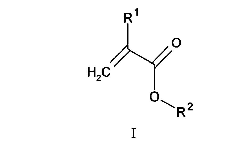
{N+(R3)(R4)-(CH2)a-N(H)-C(Y)-N(H)-(CH2)b-N+(R3)(R4)-R5}n 2n X- II
wherein: - R1 is H or C1-C4 alkyl;
- R2 is C1-C20 alkyl, which may be substituted by at least one moiety selected from the group comprising OH, unsubstituted and substituted phenyl, unsubstituted and substituted phenoxy, amino, alkylene(alkylamino), alkylene(dialkylamino), alkylene(trialkylammonium ion) and alkylene oxirane;
- R3 and R4 are independently methyl, ethyl, isopropyl, hydroxymethyl, hydroxyethyl or -CH2CH2(OCH2CH2)cOH;
- R5 is (CH2)d or {(CH2)eO(CH2)f}g;
- Y is O, S or NH;
- a, b, c, d, e and f are each independently an integer from 1 to about 6;
- g is an integer from 1 to about 4;
- n is at least 1; and
- X- is a halide (fluoride, chloride, bromide, iodide, most preferably chloride) ion.
- The above adhesion agents have turned out to be effective in preparing a copper surface for achieving good adherence of a polymeric deposit being applied thereon. Such good adhesion has particularly found out to be attained if the copper surface does not have a rough surface, but is substantially smooth. Even under these conditions good adherence of the polymeric deposit may be achieved, though hitherto it has been assumed that good adherence may only be observed if the copper surface has been made rough or is rough as prepared. This result is astonishing since a strong bond between the copper and the polymeric deposit has been believed to be only due to an enlargement of the specific surface area of the copper surface. Good adherence has been proved by visually inspecting consistency of a finest line pattern in a photo imageable photoresist laminated on a copper surface and exposed and developed and additionally by testing adherence with a tape test at such processed photo imageable photoresist layer.
- Consistency and adherence have been proved excellent. This is in spite of the fact, that the copper surface is not substantially affected by the pretreatment method of the invention, i.e., no noticeable roughening takes place when the copper surface is treated in accordance with the invention. Therefore, there is no risk as to excessive removal of copper due to the treatment as with previous methods. Such removal would particularly be important if the copper surface presented is very thin such as in semi-additive processing. Base substrates used in printed circuit board manufacturing for high-sophisticated applications comprise an electroless copper base layer which is only about 1 µm thick and onto which a photo imageable resist is laminated and processed to form a circuitry. As copper pretreatment according to the present invention does virtually not remove any copper from such thin copper base layers, there is, even in portions of the surface area, no risk of complete copper removal. Copper removal using the compounds according to the invention has emerged to be at most 0.1 to 0.2 µm of copper.
- Good adherence despite low roughness is assumed to be due to certain specific structural features present in the adhesion agent molecules which mediate adherence between the copper surface and the polymeric deposit. In the case of the heterocyclic compounds comprising at least one thiol moiety, the thiol moiety is believed to be effective in strongly bonding to the copper surface while the heterocyclic ring system is believed to be effective in strongly bonding to the polymeric deposit. In the case of the acrylic compounds having general chemical formula I, the C=O moiety of the molecule is believed to be effective in strongly bonding to the copper surface while the unsaturated structure element in the acrylic moiety of the molecule is believed to strongly bond to the polymeric deposit. In the case of the quaternary ammonium polymers having general chemical formula II, the NH-C(=Y)-NH moiety is believed to strongly bond to the copper surface while the intermediate moiety (N+(R3)(R4)-R5-N+(R3)(R4)) is believed to strongly bond to the polymeric deposit:

- The above compound (commercially available as Polyquaternium-2 of Sigma-Aldrich is the chloride salt thereof) is a preferred example of a quaternary ammonium polymer, wherein Y = O, R3, R4 = CH3 and R5 = CH2CH2-O-CH2CH2.
- The adhesion agents of the invention are applied to the copper surface by bringing the work piece into contact with the non-etching composition which contains the at least one adhesion agent. Such contacting of the non-etching adhesion composition with the work piece will be performed by dipping the work piece into the composition or by spraying the composition on the surface of the work piece.
- For the purpose of the present invention the term "alkyl" is defined herein as a group of saturated compounds having in the skeleton thereof but carbon atoms, these compounds comprising all conceivable isomers thereof. C1-C6 alkyl means methyl, ethyl, propyl, isopropyl, butyl, isobutyl, tert-butyl, pentyl, isopentyl, tert-pentyl, neo-pentyl, hexyl, 2-methyl pentyl, 3-methyl pentyl, 2,3-diethyl butyl.
- For the purpose of the present invention the term "phenyl" is defined herein as an aromatic moiety which has in its aromatic skeleton six carbon atoms.
- For the purpose of the present invention the term "oxirane" is defined herein as a three-membered cyclic radical having an oxygen atom and two carbon atoms in the ring, the most simple specimen being an epoxide ring which is an unsubstituted oxirane.
- For the purpose of the present invention the term "circuit carrier" is defined herein as a device which is used to provide electrical interconnections between various electronic components and other components mounted thereon, such as resistors, capacitors, transistors, integrated circuits, transformers, LEDs, switches, edge connectos and the like. A circuit carrier may be a printed circuit board or a hybrid circuit board or a multi chip module or the like.
- The non-etching composition providing good adherence between a smooth copper surface and a polymeric deposit, a photo imageable resist for example, is primarily composed of the at least one adhesion agent according to the invention and at least one solvent. The non-etching composition may be acidic, neutral or alkaline, more preferably slightly alkaline (pH from neutral to about 9.5). Most preferably the non-etching composition is acidic. If the non-etching composition is acidic, either the at least one adhesion agent is acidic per se, or there is at least one additional compound present in the composition which provides the composition with an acidic pH, i.e., a pH below about 7, more specifically below about 4, more preferably below about 1.5 and most preferably below about 1. The lower limit of the pH is dependent on the compound being used to adjust pH and may be above about -0.5, more preferably above about 0 and most preferably above about 0.5.
- Further, according to a preferred embodiment of the invention, the heterocyclic compounds comprising at least one thiol moiety, are preferably selected from the group comprising 1 H-1,2,4-triazole-3-thiol, 3-mercaptotriazole, 2-mercaptobenzothiazole and 2-mercaptobenzimidazole. Most preferably, 1H-1,2,4-triazole-3-thiol is used to be an adhesion agent in the sense of the present invention.
- Further, according to a preferred embodiment of the invention, in the acrylic compounds having general chemical formula I, R2 is (CH2)m-R6,
wherein: - m is an integer from 1 to 20,
- (CH2)m may be substituted in at least one of the CH2 moieties with OH and may also be branched instead of being unbranched, as (CH2)m suggests; R6 is H, phenyl, O-Phenyl, NR7R8, N+R7R8R9 Z- or an oxirane ring;
- wherein phenyl is unsubstituted or substituted, R7, R8 and R9 are, independently, H or C1-C6 alkyl, the oxirane ring is substituted or unsubstituted and Z- is an anion.
- Further, according to a preferred embodiment of the invention, in the acrylic compounds having general chemical formula I, R1 is CH3.
- Further, according to a preferred embodiment of the invention, in the acrylic compounds having general chemical formula I, the (CH2)m moiety is CH2-CH(OH)-CH2.
- Further, according to a preferred embodiment of the invention, in the acrylic compounds having general chemical formula I, phenyl is 3-(benzotriazol-2-yl)-4-hydroxy-phenyl.
- Further, according to a preferred embodiment of the invention, in the acrylic compounds having general chemical formula I, the oxirane ring is an unsubstituted epoxide ring.
- Further, according to a preferred embodiment of the invention, in the acrylic compounds having general chemical formula I, R2 is (CH2)m-R6, wherein m is an integer from 1 to 20 and R6 is H.
- Further, according to a preferred embodiment of the invention, in the acrylic compounds having general chemical formula I, m is an integer from 10 to 19 and R6 is H.
- Further, according to a preferred embodiment of the invention, in the acrylic compounds having general chemical formula I, NR7R8 is NHC(CH3)3.
- Further, according to a preferred embodiment of the invention, in the acrylic compounds having general chemical formula I, N+R7R8R9 Z- is N+(CH3)3 Z-.
- Further, according to a preferred embodiment of the invention, the acrylic compounds having general chemical formula I are selected from the group comprising methacrylic acid octadecyl ester, methacrylic acid 2-phenoxyethylester, 3-(methacryloyloxy)-2-hydroxypropyl ester, 2-[3-(2H-benzotriazol-2-yl)-4-hydroxyphenyl] ethyl methacrylate, 2-(tert-butylamino) ethyl methacrylate, 2-(methacryloyloxy)ethyl trimethylammonium methosulfate and (acryloyloxy)methyl oxirane.
- Further, according to a preferred embodiment of the invention, in the quaternary ammonium polymers having general chemical formula II, R3 and R4 are methyl.
- Further, according to a preferred embodiment of the invention, in the quaternary ammonium polymers having general chemical formula II, a and b are 3.
- Further, according to a preferred embodiment of the invention, in the quaternary ammonium polymers having general chemical formula II, Y is O.
- Further, according to a preferred embodiment of the invention, in the quaternary ammonium polymers having general chemical formula II, R5 is {(CH2)eO(CH2)f}g.
- Further, according to a preferred embodiment of the invention, in the quaternary ammonium polymers having general chemical formula II, e and f are 2.
- Further, according to a preferred embodiment of the invention, in the quaternary ammonium polymers having general chemical formula II, g is 1.
- Further, according to a preferred embodiment of the invention, in the quaternary ammonium polymers having general chemical formula II, X- is chloride
- Further, according to a preferred embodiment of the invention, the quaternary ammonium polymer has the following general chemical formula IIA:

- Preferably the concentration of the adhesion agent in the non-etching composition of the invention is at least about 1 mg/l, more preferably at least about 2 mg/l, even more preferably at least about 5 mg/l and most preferably at least about 10 mg/l and may be for example about 10 or about 15 or about 20 or about 30 mg/l. The concentration of the adhesion agent in the non-etching composition of the invention is at most about 1000 mg/l, more preferably at most about 500 mg/l, even more preferably at most about 200 mg/l, even more preferably at most about 100 mg/l and most preferably at most about 50 mg/l. Any range delimited by the above values may be used to define the concentration range of the adhesion agent. If more than one adhesion agent is used in the non-etching composition, the above concentration values are meant to define the sum of all concentrations of adhesion agents contained in the composition.
- In order to assure that copper is virtually unaffected by the non-etching composition, this composition is free of an oxidant for copper or the copper alloy. Therefore, this composition does not etch copper. Therefore, the composition is free of hydrogen peroxide, any salts of peroxodisulfate, any salt of caroate and of any other peroxide like perboric acid or performic acid, for example.
- As stated above, the non-etching composition further comprises at least one mineral acid or at least one organic acid. In general, these acids render the composition acidic, such that the pH thereof is attained to be in the range defined herein above.
- More preferably, the mineral acid is selected from the group comprising sulfuric acid and phosphoric acid. Most preferably it is sulfuric acid. The concentration of the sulfuric acid is preferably at least about 5 ml, more preferably at least about 50 ml, even more preferably at least about 75 ml and most preferably at least about 100 ml concentrated sulfuric acid in 1 l of the composition and is preferably at most about 300 ml, more preferably at most about 250 ml, even more preferably about 200 ml and most preferably at most about 150 ml concentrated sulfuric acid in 1 l of the composition.
- As stated above, the method of the present invention comprises: (a) providing the work piece and (b) bringing the work piece into contact with the non-etching composition of the invention.
- If the adhesion agent is a heterocyclic compound comprising at least one thiol moiety or an acrylic compound having general chemical formula I, the copper surface to be treated is preferably first contacted with an aqueous solution of a mineral acid, to remove any soil from the copper surface prior to having the adhesion agent impacting on the copper surface. This mineral acid may be sulfuric acid. An aqueous solution of sulfuric acid may have a concentration of from about 10 ml to about 150 ml, more preferably about 20 ml to about 100 ml and is most preferably about 50 ml concentrated sulfuric acid in 1 l of this solution for example.
- Alternatively, in a preferred embodiment of the present invention, the method of the invention further comprises: (c) bringing the work pieces into contact with at least one phosphonic acid compound, if the adhesion agent is selected from the group comprising the quaternary ammonium polymers having general chemical formula II. This post-treatment provides for an additional adhesion improvement.
- The phosphonic acid compounds are preferably selected from the group comprising hydroxyethylidene diphosphonic acid, amino tri(methylene phosphonic acid), diethylenetriamine penta(methylene phosphonic acid), polyamino phosphonic acid, bis(hexamethylene triamine penta(methylene phosphonic acid)) and 2-
phosphonobutane 1,2,4-tricarboxylic acid or the salts thereof. Most preferably the phosphonic acid compound is hydroxyethyliden diphosphonic acid (INN: etidronic acid). A 60 wt.-% aqueous solution of this compound is sold under the trade name Dequest® 2010 (Thermophos Deutschland, DE). - The phosphonic acid compound is used as an aqueous solution thereof to post-treat the copper surfaces, if the adhesion agent is selected from the group comprising quaternary ammonium polymers having general chemical formula II. This aqueous solution contains the at least one phosphonic acid compound at a concentration of 0.01 to 100 g, preferably 1 to 10g per liter of the solution, for example, wherein this range refers to the overall concentration of all phosphonic acid compounds in the aqueous solution.
- In an alternative embodiment of the present invention, if the adhesion agent is selected from the group comprising quarternary ammonium polymers having general chemical formula II, instead of post-treating the copper surfaces with at least one phosphonic acid compound, the method further comprises: (c) bringing the work piece into contact with at least one acrylic compound having general chemical formula I. This also provides for an additional adhesion improvement.
- Therefore, the method of the invention is performed easily, i.e., with only a few process steps being required.
- The non-etching composition may be used to pre-treat a copper surface in a process used to manufacture circuit carriers, more preferably printed circuit boards. In this case the polymeric deposit is a resist coating, more preferably a photo imageable resist.
- For the manufacture of a circuit carrier, more preferably a printed circuit board,
- (a) a substrate is generally used which comprises a copper coating on at least one side thereof and which is further provided with through-holes which serve to electrically contact individual circuit planes within the carrier;
- (b) this substrate is first copper coated on the outer sides and on the hole walls, in general with electroless copper plating only or with electroless and subsequently electrolytic copper plating or with electrolytic copper plating only.
- Further processing depends on the methods involved:
- In the panel plating process variation, in general, a copper clad (17 µm thick copper outer layer) material is used, which is drilled to form the through-holes and is then electrolytic copper-plated to provide electrical conductivity in the through-holes. This method further comprises the following general method steps:
- (c) pre-treating the copper layer with the non-etching composition of the invention;
- (d) applying a resist to the coppered surface and imaging the resist, thereby forming resist voids;
- (e) removing copper which is exposed in the resist voids; and
- (f) stripping the resist from the surface of the copper surface; the resist is preferably a photo imageable resist.
- In the semi-additive plating process variation, in general, a substrate material is used, which is provided on the outer sides with a dielectric surface and which, after having been drilled to form the through-holes, is copper-plated to form a thin copper layer on the outer sides. In this case, a conventional printed circuit board may be used for example which is additionally provided with a resin coating on the outer sides to form the dielectric surface. This method further comprises the following general method steps:
- (c) pre-treating the copper layer on the outer sides of the substrate with the non-etching composition of the invention;
- (d) applying a resist to the coppered surface and imaging the resist, thereby forming resist voids;
- (e) depositing copper in the resist voids;
- (f) stripping the resist from the copper surface; and
- (g) etching off the copper in those regions which have previously been covered by the resist; the resist is preferably a photo imageable resist.
- Photo imageable resists are usually applied as a dry film or a liquid film. The dry film is a common imageable photoresist consisting of a cover or support sheet, a photoimageable layer, and a protective layer, as provided by DuPont, Hitachi. Liquid photo resist are applied directly onto the copper layer by, e.g., roller coating, curtain coating, without protective layers (e.g., Huntsman, Rohm & Haas, Atotech).
- These methods are well-known in the art and are for example described in: Coombs, Printed Circuits Handbook 5th Editi on, or have been published in the internet under URL http://www.circuitree.com/copyright/2FBNP_GUID_9-5-2006_A_10000000000000244144 &message=1 or under URL http://www.circuitree.com/Articles/Column/16bc3b84a7809010 VgnVCM100000f932a8c0_, both being accessed on 19 February 2008, the disclosure thereof being entirely incorporated herein by reference.
- The methods described herein may be performed in a conventional dip-tank technique (vertical processing) or in a conveyorized machine (horizontal processing).
- To illustrate the present invention, examples are given in the following. These do not limit the scope of the invention, but are rather specific embodiments of the invention:
- Fig. 1
- shows an artwork of fine lines used for imaging a photo imageable resist;
- Fig. 2
- shows results from pre-treating a coppered substrate with compounds A, E (influence of concentration) and are compared to treatment with H2SO4;
- Fig. 3
- shows results from pre-treating a coppered substrate with compounds B, E (influence of concentration) and are compared to treatment with H2SO4;
- Fig. 4
- shows results from pre-treating a coppered substrate with compounds C, E (influence of concentration) and are compared to treatment with H2SO4;
- Fig. 5
- shows results from pre-treating a coppered substrate with compounds D, E (influence of concentration) and are compared to treatment with H2SO4;
- Fig. 6
- shows results from pre-treating a coppered substrate with compounds A, B, C, D, E (10 mg/l) and are compared to treatment with H2SO4;
- Fig. 7
- shows results from pre-treating a coppered substrate with compounds B, D, E (influence of solvent; Type A material) and are compared to treatment with H2SO4;
- Fig. 8
- shows results from pre-treating a coppered substrate with compounds B, D, E (influence of solvent; Type B material) and are compared to treatment with H2SO4;
- Fig. 9
- shows results from pre-treating a coppered substrate with compounds A, C, E (Type A material) and are compared to treatment with H2SO4;
- Fig. 10
- shows results from pre-treating a coppered substrate with compounds A, C, E (Type B material) and are compared to treatment with H2SO4;
- Fig. 11
- shows results from pre-treating a coppered substrate with compounds D, E, F and F + post dip (PD) (Type A material) and are compared to treatment with H2SO4;
- Fig. 12
- shows a representation of the data of
Fig. 11 , being illustrated as a [%] improvement over the treatment with H2SO4. - All tested compounds were first prepared to be dissolved in a standard solution containing 1 g of the Compound in 1 l of deionized water (acrylic Compounds B, D and heterocyclic Compound E) or in 1 l of ethylene glycol monobutylether (acrylic Compounds A, C).
Afterwards, to prepare adhesion agent compositions, all standard solutions were respectively added to solutions comprising 130ml 50 vol-% sulfuric acid in 1 l of deionized water in an amount to achieve the desired concentration of the compound in the adhesion agent composition (1, 10, 20, 50 mg/l). 7,5 cm x 15 cm large test panels were prepared from the following material:Type A) Copper clad (35 µm copper) FR4 dielectric laminate, which was provided with an electroless copper layer of about 1 µm thickness (Printoganth® PV, Atotech Deutschland, DE); Type B) Copper Clad with 18 µm DC galvanized copper which was provided with an electroless copper layer of about 1 µm thickness (Printoganth® PV, Atotech Deutschland, DE) (represents very smooth surface) Type C) FR4 panels having copper clad (35 µm copper) which was further coated with an epoxy resin coating (Ajinomoto GX-13 from Ajinomoto Fine-Techno Co., JP), which was thereafter further coated with an electroless copper layer of about 1 µm thickness. - The test panels which were designated to be treated with Compounds A, B, C and D (acrylic Compounds having general chemical formula I) or with 1 H-1,2,4-triazole-3-thiol (heterocyclic compound comprising at least one thiol moiety), Compound E, were first treated with a 5 vol-% sulfuric acid solution, thereafter rinsed and then treated with the adhesion agent composition. The test panels, which were designated to be treated with Compound E, were rinsed after the treatment with the adhesion agent composition. The test panels, which were designated to be treated with Compound F, were, after the treatment with the adhesion agent composition, rinsed and thereafter treated with an aqueous solution of Dequest® 2010 (Thermophos Deutschland, DE) at a concentration of 5 g Dequest® 2010 per liter.
- For the treatment with the adhesion agent composition, all test panels were sprayed with these compositions for 30 - 45 s at 35 - 45°C onto the surface thereof. After the respective last treatment step the panels were rinsed in deionized water and finally dried.
- Further, reference panels were prepared using 5 vol-% sulfuric acid (Reference Sample X).
- Afterwards, these test panels were laminated with a fine line dry film (25 µm thickness) using a hot-roll laminator. Using an artwork having 10 µm, 12 µm, 15 µm, 20 µm and 25 µm line width with varying spaces between the lines (
Fig. 1 ), the dry film was exposed using a UV exposure unit. Unexposed film was removed with standard sodium carbonate developer solution, thereby removing the film except on the line features. - After developing, rinsing and drying, the test panels were evaluated by counting the number of completely intact lines for every line thickness. If all 36 lines remained completely intact during development (or after a tape test), the respective panel was assigned a value of 100 %. In specific cases, a tape test was additionally performed after first visual inspection as described before. For this purpose, a tape (Scotch® Tape 600, 3M, US) was pressed onto the dry film pattern and the integrity of the lines was again visually inspected (marked with "TT" in the following Figs.).
- Finally the panels prepared as described before were electroplated with copper using a vertical Cupracid® HL plating bath (Atotech Deutschland, DE), thereafter rinsed and finally dried. The panels were again visually inspected to detect under-plating of copper under the resist. Such under-plating would point to a lack of resist adherence to the copper surface during the coppering step. Visual inspection also included copper-to-copper adherence.
- First tests were performed on test panels Type A. The results obtained with the acrylic Compounds A, B, C and D were in each case compared to results obtained with heterocyclic Compound E and with Reference Sample X (
Figs. 2 - 5 ). As there could not be detected any significant difference between the individual Compounds and the Reference Sample being tested before applying a Scotch® tape, the graphs shown inFigs. 2 - 5 refer to line integrity after tape testing. - A concentration of Compounds A, B, C, D and E of 10 - 20 mg/l was found to give best performance. Adhesion performance of all Compounds was superior compared to Reference Sample X. A comparison of the results for 10 mg/l compositions containing the Compounds and for the Reference Sample X is shown in
Fig. 6 . Interestingly, Compounds A and C performed in most cases a little worse than Compounds B and D. This difference was believed to be due to the solvent being used to prepare the standard solutions. Therefore, further tests were performed to investigate the influence of the solvent and the influence of the type of test panels. - This experiment was performed to observe the effect of the solvent and of the panel type on line integrity. Therefore, all tests were made on test panels Type A and Type B. Furthermore, acrylic Compounds C and D were both dissolved in deionized water or in ethylene glykol monobutylether, resp., in order to directly compare the influence of this solvent. The concentration of these Compounds in the adhesion agent composition was 10 mg/l.
- The results obtained after tape testing are shown in
Fig. 7 (Type A material) andFig. 8 (Type B material). - For Type A material, Compound B being dissolved in ethylene glykol monobutylether to give the standard solution, gave similar results as Compound B being dissolved in water on Type A material. Performance of Compound D was always better without the ether solvent. Compared to Compound E, all results were more or less similar for all Compounds (except for Reference Sample X) for 12 µm lines, but were different for wider lines. In these latter cases Compound E resulted in higher adherence of the resist.
- For Type B material, the difference between the Compounds was found to be more pronounced in that Compound B without ether solvent and Compound E were better than the rest.
- Further results obtained with Type A and Type B material using Compounds A and C, dissolved in the ether solvent, and Compound E are shown in
Fig. 9 (Type A material) andFig. 10 (Type B material). - On Type A material, all three Compounds presented similar results on all lines.
- On Type B material, Compound A had a better performance than Compound C, but was worse than Compound E.
- In these experiments Compounds D, E and F (concentration: 1 - 100 mg/l) were investigated, with F being investigated with and without further post-dip in an aqueous solution of 1-
hydroxyethylidene Fig. 11 ). Visual inspection was made before and after tape testing ("TT"). - Further, an alternative representation of the data obtained is shown in the diagram of
Fig. 12 , this diagram showing the improvement in [%] over treatment with Sample X. - The results of these tests after tape testing show that Compound D has a slightly worse performance than Compound E and that performance of Compound F is comparable to that of Compound E.
- Pre-treatment with adhesion agent compositions containing Compounds A, B, C, D and E was performed (
concentration 10 mg/l) and the dry film applied, exposed and developed as before. The panels were then electrolytically copper plated to achieve a 15 µm thick copper deposit. - Visual inspection showed that no under-plating of copper under the resist has occurred. After tape testing on the copper surface, no pealing-off of the plated copper could be detected. This result points to a good copper-to-copper adherence.
Table 1 - Test Compounds Compound Chemical Name Trade Name Available from Compound A 2-[3-(2H-benzotriazol-2-yl)-4-hydroxyphenyl] ethyl methacrylate Sigma-Aldrich Compound B 2-(tert-butylamino) ethyl methacrylate Sigma-Aldrich Compound C methacrylic acid octadecyl ester Sigma-Aldrich Compound D 2-(methacryloyloxy)ethyl trimethylammonium methosulfate Sigma- Aldrich Compound E 1,2,4-triazole-3-thiol Sigma-Aldrich Compound F poly{bis(2-chloroethylether-alt-1,3-bis[3-(diemthylamino)propyl]urea}, quaternized solution Polyquaternium-2 Sigma-Aldrich
Claims (35)
- A non-etching composition for the treatment of copper or copper alloys, the composition comprising at least one adhesion agent selected from the group comprising heterocyclic compounds comprising at least one thiol moiety, acrylic compounds having general chemical formula I:

{N+(R3)(R4)-(CH2)a-N(H)-C(Y)-N(H)-(CH2)b-N+(R3)(R4)-R5}n 2n X- II
wherein:R1 is H or C1-C4 alkyl;R2 is C1-C20 alkyl, which may be substituted by at least one moiety selected from the group comprising OH, unsubstituted and substituted phenyl, unsubstituted and substituted phenoxy, amino, alkylene(alkylamino), alkylene(dialkylamino), alkylene(trialkylammonium ion) and alkylene oxirane;R3 and R4 are independently methyl, ethyl, isopropyl, hydroxymethyl, hydroxyethyl or -CH2CH2(OCH2CH2)cOH;R5 is (CH2)d or {(CH2)eO(CH2)f]g;Y is O, S or NH;a, b, c, d, e and f are each independently an integer from 1 to about 6;g is an integer from 1 to about 4;n is at least 1; andX- is a halide ion. - The non-etching composition for the treatment of copper or copper alloys according to claim 1, wherein the heterocyclic compounds comprising at least one thiol moiety are selected from the group comprising 1 H-1,2,4-triazole-3-thiol, 3-mercaptotriazole, 2-mercaptobenzothiazole and 2-mercaptobenzimidazole.
- The non-etching composition for the treatment of copper or copper alloys according to any one of the preceding claims, wherein R2 is (CH2)m-R6,
wherein:m is an integer from 1 to 20,(CH2)m may be substituted in at least one of the CH2 moieties with OH;R6 is H, phenyl, O-Phenyl, NR7R8, N+R7R8R9 Z- or an oxirane ring;
wherein phenyl is unsubstituted or substituted, R7, R8 and R9 are, independently, H or C1-C6 alkyl, the oxirane ring is substituted or unsubstituted and Z- is an anion. - The non-etching composition for the treatment of copper or copper alloys according to any one of the preceding claims, wherein R1 is CH3.
- The non-etching composition for the treatment of copper or copper alloys according to any one of the preceding claims, wherein the (CH2)m moiety is CH2-CH(OH)-CH2.
- The non-etching composition for the treatment of copper or copper alloys according to any one of the preceding claims, wherein phenyl is 3-(benzotriazol-2-yl)-4-hydroxy-phenyl.
- The non-etching composition for the treatment of copper or copper alloys according to any one of the preceding claims, wherein the oxirane ring is an unsubstituted epoxide ring.
- The non-etching composition for the treatment of copper or copper alloys according to any one of the preceding claims, wherein R2 is (CH2)m-R6, wherein m is an integer from 1 to 20 and R6 is H.
- The non-etching composition for the treatment of copper or copper alloys according to any one of the preceding claims, wherein m is an integer from 10 to 19 and R6 is H.
- The non-etching composition for the treatment of copper or copper alloys according to any one of the preceding claims, wherein NR7R8 is NHC(CH3)3.
- The non-etching composition for the treatment of copper or copper alloys according to any one of the preceding claims, wherein N+R7R8R9 Z- is N+(CH3)3 Z-.
- The non-etching composition for the treatment of copper or copper alloys according to any one of the preceding claims, wherein the acrylic compound having general chemical formula I is selected from the group comprising methacrylic acid octadecyl ester, methacrylic acid 2-phenoxyethylester, 3-(methacryloyloxy)-2-hydroxypropyl ester, 2-[3-(2H-benzotriazol-2-yl)-4-hydroxyphenyl] ethyl methacrylate, 2-(tert-butylamino) ethyl methacrylate, 2-(methacryloyloxy)ethyl trimethylammonium methosulfate and (acryloyloxy)methyl oxirane.
- The non-etching composition for the treatment of copper or copper alloys according to any one of the preceding claims, wherein R3 and R4 are methyl.
- The non-etching composition for the treatment of copper or copper alloys according to any one of the preceding claims, wherein a and b are 3.
- The non-etching composition for the treatment of copper or copper alloys according to any one of the preceding claims, wherein Y is O.
- The non-etching composition for the treatment of copper or copper alloys according to any one of the preceding claims, wherein R5 is {(CH2)eO(CH2)f}g.
- The non-etching composition for the treatment of copper or copper alloys according to any one of the preceding claims, wherein e and f are 2.
- The non-etching composition for the treatment of copper or copper alloys according to any one of the preceding claims, wherein g is 1.
- The non-etching composition for the treatment of copper or copper alloys according to any one of the preceding claims, wherein X- is chloride.
- The non-etching composition for the treatment of copper or copper alloys according to any one of the preceding claims, wherein the quaternary ammonium polymer having general chemical formula II has the following general chemical formula IIA:

- The non-etching composition for the treatment of copper or copper alloys according to any one of the preceding claims, wherein the adhesion agent is contained in the composition at a concentration of from 1 mg/l to 1000 mg/l.
- The non-etching composition for the treatment of copper or copper alloys according to any one of the preceding claims, wherein the composition is free of an oxidant for copper or the copper alloy.
- The non-etching composition for the treatment of copper or copper alloys according to any one of the preceding claims, further comprising at least one mineral acid or at least one organic acid.
- The non-etching composition for the treatment of copper or copper alloys according to any one of the preceding claims, wherein the mineral acid is selected from the group comprising sulfuric acid and phosphoric acid.
- A method of preparing a work piece having a copper or copper alloy surface for subsequent coating the copper or copper alloy surface with a polymeric deposit, comprising (a) providing the work piece and (b) bringing the work piece into contact with the non-etching composition according to any one of claims 1 - 24.
- The method of preparing a work piece having a copper or copper alloy surface for subsequent coating the copper or copper alloy surface with a polymeric deposit according to claim 25, wherein the work piece is brought into contact with the non-etching composition by dipping the work piece into the composition or by spraying the composition on the surface of the work piece.
- The method of preparing a work piece having a copper or copper alloy surface for subsequent coating the copper or copper alloy surface with a polymeric deposit according to any one of claims 25 and 26, wherein the method further comprises: (c) bringing the work piece into contact with at least one phosphonic acid compound, if the adhesion agent is selected from the group comprising the quaternary ammonium polymers having general chemical formula II.
- The method of preparing a work piece having a copper or copper alloy surface for subsequent coating the copper or copper alloy surface with a polymeric deposit according to claim 27, wherein the phosphonic acid compound is selected from the group comprising hydroxyethylidene diphosphonic acid, amino tri(methylene phosphonic acid), diethylenetriamine penta(methylene phosphonic acid), polyamino phosphonic acid, bis(hexamethylene triamine penta(methylene phosphonic acid)) and 2-phosphonobutane 1,2,4-tricarboxylic acid.
- The method of preparing a work piece having a copper or copper alloy surface for subsequent coating the copper or copper alloy surface with a polymeric deposit according to any one of claims 27 and 28, wherein the phosphonic acid compound is hydroxyethyliden diphosphonic acid.
- The method of preparing a work piece having a copper or copper alloy surface for subsequent coating the copper or copper alloy surface with a polymeric deposit according to any one of claims 25 - 27, wherein the method further comprises: (c) bringing the work piece into contact with at least one acrylic compound having general chemical formula I, if the adhesion agent is selected from the group comprising the quaternary ammonium polymers having general chemical formula II.
- The method of preparing a work piece having a copper or copper alloy surface for subsequent coating the copper or copper alloy surface with a polymeric deposit according to any one of claims 25 - 30, wherein the work piece is a circuit carrier having a copper surface and wherein the polymeric deposit is a resist coating.
- A method of forming copper structures on a circuit carrier substrate, comprising (a) providing the circuit carrier substrate, (b) coppering the surface of the circuit carrier substrate using an electroless copper process, (c) performing the method according to any one of claims 25 - 31 on the coppered surface, (d) applying a resist to the coppered surface and imaging the resist, thereby forming resist voids, (e) depositing copper in the resist voids, (f) stripping the resist from the copper surface, and (g) etching off the copper in those regions which have previously been covered by the resist.
- The method of forming copper structures on a circuit carrier substrate according to claim 32, wherein the resist is a photo imageable resist.
- A method of forming copper structures on a circuit carrier substrate, comprising (a) providing the circuit carrier substrate, (b) electroless and electrolytic coppering the surface of the circuit carrier substrate, (c) performing the method according to any one of claims 25 - 31 on the coppered surface, (d) applying a resist to the coppered surface and imaging the resist, thereby forming resist voids, (e) removing copper which is exposed in the resist voids, and (f) stripping the resist from the surface of the copper surface.
- The method of forming copper structures on a circuit carrier substrate according to claim 34, wherein the resist is a photo imageable resist.
Priority Applications (8)
| Application Number | Priority Date | Filing Date | Title |
|---|---|---|---|
| EP08075181A EP2099268A1 (en) | 2008-03-07 | 2008-03-07 | Non-etching adhesion composition, method of preparing a work piece and method of forming coppper structures on a circuit carrier substrate |
| US12/867,112 US8945298B2 (en) | 2008-03-07 | 2009-02-27 | Non-etching non-resist adhesion composition and method of preparing a work piece |
| PCT/EP2009/001605 WO2009109391A1 (en) | 2008-03-07 | 2009-02-27 | Non-etching non-resist adhesion composition and method of preparing a work piece |
| JP2010549061A JP5538243B2 (en) | 2008-03-07 | 2009-02-27 | Non-etching and non-resist adhesive composition and processing method of processed parts |
| KR1020107019893A KR101614169B1 (en) | 2008-03-07 | 2009-02-27 | Non-etching non-resist adhesion composition and method of preparing a work piece |
| EP09717965.9A EP2248402B1 (en) | 2008-03-07 | 2009-02-27 | Non-etching non-resist adhesion composition and method of preparing a work piece |
| CN2009801028321A CN101926235B (en) | 2008-03-07 | 2009-02-27 | Non-etching non-resist adhesion composition and method of preparing work piece |
| TW098106406A TWI457469B (en) | 2008-03-07 | 2009-02-27 | Non-etching non-resistive adhesive composition and method for preparing the same |
Applications Claiming Priority (1)
| Application Number | Priority Date | Filing Date | Title |
|---|---|---|---|
| EP08075181A EP2099268A1 (en) | 2008-03-07 | 2008-03-07 | Non-etching adhesion composition, method of preparing a work piece and method of forming coppper structures on a circuit carrier substrate |
Publications (1)
| Publication Number | Publication Date |
|---|---|
| EP2099268A1 true EP2099268A1 (en) | 2009-09-09 |
Family
ID=39666196
Family Applications (2)
| Application Number | Title | Priority Date | Filing Date |
|---|---|---|---|
| EP08075181A Withdrawn EP2099268A1 (en) | 2008-03-07 | 2008-03-07 | Non-etching adhesion composition, method of preparing a work piece and method of forming coppper structures on a circuit carrier substrate |
| EP09717965.9A Active EP2248402B1 (en) | 2008-03-07 | 2009-02-27 | Non-etching non-resist adhesion composition and method of preparing a work piece |
Family Applications After (1)
| Application Number | Title | Priority Date | Filing Date |
|---|---|---|---|
| EP09717965.9A Active EP2248402B1 (en) | 2008-03-07 | 2009-02-27 | Non-etching non-resist adhesion composition and method of preparing a work piece |
Country Status (7)
| Country | Link |
|---|---|
| US (1) | US8945298B2 (en) |
| EP (2) | EP2099268A1 (en) |
| JP (1) | JP5538243B2 (en) |
| KR (1) | KR101614169B1 (en) |
| CN (1) | CN101926235B (en) |
| TW (1) | TWI457469B (en) |
| WO (1) | WO2009109391A1 (en) |
Cited By (2)
| Publication number | Priority date | Publication date | Assignee | Title |
|---|---|---|---|---|
| WO2011147448A1 (en) * | 2010-05-26 | 2011-12-01 | Atotech Deutschland Gmbh | Composition and method for micro etching of copper and copper alloys |
| EP4279634A1 (en) * | 2022-05-17 | 2023-11-22 | Atotech Deutschland GmbH & Co. KG | Method for nano etching of copper and copper alloy surfaces |
Families Citing this family (10)
| Publication number | Priority date | Publication date | Assignee | Title |
|---|---|---|---|---|
| EP2537962A1 (en) * | 2011-06-22 | 2012-12-26 | Atotech Deutschland GmbH | Method for copper plating |
| JP6225467B2 (en) * | 2012-06-06 | 2017-11-08 | 三菱瓦斯化学株式会社 | Copper foil for printed wiring board, method for producing the same, and printed wiring board using the copper foil |
| EP2754732B1 (en) | 2013-01-15 | 2015-03-11 | ATOTECH Deutschland GmbH | Aqueous composition for etching of copper and copper alloys |
| JP5615401B1 (en) * | 2013-05-14 | 2014-10-29 | 石原ケミカル株式会社 | Copper fine particle dispersion, conductive film forming method, and circuit board |
| US10506723B2 (en) | 2014-12-02 | 2019-12-10 | International Business Machines Corporation | Enhanced substrate includes a carbene-coated metal foil laminated to a substrate that includes glass fiber impregnated with a base polymer |
| US10481496B2 (en) * | 2017-06-28 | 2019-11-19 | International Business Machines Corporation | Forming conductive vias using a light guide |
| EP3567993B1 (en) * | 2018-05-08 | 2022-02-23 | Atotech Deutschland GmbH & Co. KG | A method for increasing adhesion strength between a surface of copper or copper alloy and an organic layer, and acidic aqueous non-etching protector solution |
| CN111748816B (en) * | 2019-03-29 | 2022-12-02 | 东友精细化工有限公司 | Silver thin film etching solution composition, etching method and metal pattern forming method |
| EP3922755A1 (en) | 2020-06-12 | 2021-12-15 | ATOTECH Deutschland GmbH | An aqueous basic etching composition for the treatment of surfaces of metal substrates |
| CN114231982B (en) * | 2021-12-20 | 2023-07-18 | 昆山市板明电子科技有限公司 | Self-etching copper surface bonding agent and preparation method thereof |
Citations (10)
| Publication number | Priority date | Publication date | Assignee | Title |
|---|---|---|---|---|
| US3645772A (en) * | 1970-06-30 | 1972-02-29 | Du Pont | Process for improving bonding of a photoresist to copper |
| US4372913A (en) * | 1965-09-20 | 1983-02-08 | Max Klein | Polymerization, and corrosion resistance, enhancement by acid addition salts of methacrylic acid and a 2-mono (lower) alkylaminoethyl methacrylate or polymers of these salts |
| EP0215670A2 (en) * | 1985-09-16 | 1987-03-25 | W.R. Grace & Co.-Conn. | Anti-corrosion composition |
| EP0422229A1 (en) * | 1989-01-25 | 1991-04-17 | Nippon Petrochemicals Company, Limited | Adhesive resin composition, preparation thereof, and laminate comprising same |
| EP0890660A1 (en) | 1997-07-08 | 1999-01-13 | MEC CO., Ltd. | Microetching agent for copper or copper alloys |
| WO2002004706A1 (en) | 2000-07-07 | 2002-01-17 | Atotech Deutschland Gmbh | Acidic treatment liquid and method of treating copper surfaces |
| EP1209253A2 (en) * | 2000-11-28 | 2002-05-29 | Shipley Co. L.L.C. | Process for treating adhesion promoted metal surfaces with epoxy resins |
| WO2005033364A1 (en) * | 2003-09-30 | 2005-04-14 | Basf Aktiengesellschaft | Method for pickling metallic surfaces by using alkoxylated alkynols |
| US20060210819A1 (en) * | 2005-03-15 | 2006-09-21 | Dueber Thomas E | Polyimide composite coverlays and methods and compositions relating thereto |
| US20070003860A1 (en) * | 2003-04-11 | 2007-01-04 | Takashi Takeda | Substrate adhesion improver for photosensitive resin composition and photosensitive resin composition containing the same |
Family Cites Families (8)
| Publication number | Priority date | Publication date | Assignee | Title |
|---|---|---|---|---|
| ZA757987B (en) | 1975-12-23 | 1976-12-29 | Dynachem Corp | Adhesion promoters for polymerizable films |
| JPS61266241A (en) * | 1985-05-21 | 1986-11-25 | 株式会社日立製作所 | Surface treating method of copper |
| JP4309602B2 (en) | 2001-04-25 | 2009-08-05 | メック株式会社 | Method for improving adhesion between copper or copper alloy and resin, and laminate |
| DE10345801A1 (en) * | 2003-09-30 | 2005-04-14 | Basf Ag | Pickling metal surface, e.g. iron, steel, zinc, brass or aluminum, especially strip, uses acid aqueous composition containing ethoxylated or propoxylated prop-1-yn-3-ol or but-2-yn-1,4-diol as inhibitor |
| JP2005290495A (en) * | 2004-04-01 | 2005-10-20 | Asahi Denka Kogyo Kk | Copper-containing material roughening agent, copper-containing material roughening method, copper-containing material roughening agent additive, and copper-containing material roughening agent manufacturing method |
| JP2006080324A (en) * | 2004-09-10 | 2006-03-23 | Sumitomo Bakelite Co Ltd | Semiconductor lead frame and semiconductor device |
| TW200626358A (en) * | 2004-11-30 | 2006-08-01 | Nippon Steel Chemical Co | Copper-clad laminate |
| JP2006182019A (en) * | 2004-11-30 | 2006-07-13 | Nippon Steel Chem Co Ltd | Copper clad laminate |
-
2008
- 2008-03-07 EP EP08075181A patent/EP2099268A1/en not_active Withdrawn
-
2009
- 2009-02-27 US US12/867,112 patent/US8945298B2/en active Active
- 2009-02-27 TW TW098106406A patent/TWI457469B/en not_active IP Right Cessation
- 2009-02-27 KR KR1020107019893A patent/KR101614169B1/en not_active Expired - Fee Related
- 2009-02-27 CN CN2009801028321A patent/CN101926235B/en not_active Expired - Fee Related
- 2009-02-27 EP EP09717965.9A patent/EP2248402B1/en active Active
- 2009-02-27 WO PCT/EP2009/001605 patent/WO2009109391A1/en not_active Ceased
- 2009-02-27 JP JP2010549061A patent/JP5538243B2/en not_active Expired - Fee Related
Patent Citations (10)
| Publication number | Priority date | Publication date | Assignee | Title |
|---|---|---|---|---|
| US4372913A (en) * | 1965-09-20 | 1983-02-08 | Max Klein | Polymerization, and corrosion resistance, enhancement by acid addition salts of methacrylic acid and a 2-mono (lower) alkylaminoethyl methacrylate or polymers of these salts |
| US3645772A (en) * | 1970-06-30 | 1972-02-29 | Du Pont | Process for improving bonding of a photoresist to copper |
| EP0215670A2 (en) * | 1985-09-16 | 1987-03-25 | W.R. Grace & Co.-Conn. | Anti-corrosion composition |
| EP0422229A1 (en) * | 1989-01-25 | 1991-04-17 | Nippon Petrochemicals Company, Limited | Adhesive resin composition, preparation thereof, and laminate comprising same |
| EP0890660A1 (en) | 1997-07-08 | 1999-01-13 | MEC CO., Ltd. | Microetching agent for copper or copper alloys |
| WO2002004706A1 (en) | 2000-07-07 | 2002-01-17 | Atotech Deutschland Gmbh | Acidic treatment liquid and method of treating copper surfaces |
| EP1209253A2 (en) * | 2000-11-28 | 2002-05-29 | Shipley Co. L.L.C. | Process for treating adhesion promoted metal surfaces with epoxy resins |
| US20070003860A1 (en) * | 2003-04-11 | 2007-01-04 | Takashi Takeda | Substrate adhesion improver for photosensitive resin composition and photosensitive resin composition containing the same |
| WO2005033364A1 (en) * | 2003-09-30 | 2005-04-14 | Basf Aktiengesellschaft | Method for pickling metallic surfaces by using alkoxylated alkynols |
| US20060210819A1 (en) * | 2005-03-15 | 2006-09-21 | Dueber Thomas E | Polyimide composite coverlays and methods and compositions relating thereto |
Non-Patent Citations (1)
| Title |
|---|
| K.H.DIETZ, DRY FILM PHOTORESIST PROCESSING TECHNOLOGY, 2001 |
Cited By (4)
| Publication number | Priority date | Publication date | Assignee | Title |
|---|---|---|---|---|
| WO2011147448A1 (en) * | 2010-05-26 | 2011-12-01 | Atotech Deutschland Gmbh | Composition and method for micro etching of copper and copper alloys |
| US8758634B2 (en) | 2010-05-26 | 2014-06-24 | Atotech Deutschland Gmbh | Composition and method for micro etching of copper and copper alloys |
| EP4279634A1 (en) * | 2022-05-17 | 2023-11-22 | Atotech Deutschland GmbH & Co. KG | Method for nano etching of copper and copper alloy surfaces |
| WO2023222701A1 (en) * | 2022-05-17 | 2023-11-23 | Atotech Deutschland GmbH & Co. KG | Method for nano etching of copper and copper alloy surfaces |
Also Published As
| Publication number | Publication date |
|---|---|
| US8945298B2 (en) | 2015-02-03 |
| KR20100126355A (en) | 2010-12-01 |
| WO2009109391A1 (en) | 2009-09-11 |
| TWI457469B (en) | 2014-10-21 |
| CN101926235A (en) | 2010-12-22 |
| JP2011517324A (en) | 2011-06-02 |
| CN101926235B (en) | 2013-04-10 |
| KR101614169B1 (en) | 2016-04-20 |
| JP5538243B2 (en) | 2014-07-02 |
| TW200944616A (en) | 2009-11-01 |
| EP2248402A1 (en) | 2010-11-10 |
| US20100323099A1 (en) | 2010-12-23 |
| EP2248402B1 (en) | 2019-05-01 |
Similar Documents
| Publication | Publication Date | Title |
|---|---|---|
| EP2248402B1 (en) | Non-etching non-resist adhesion composition and method of preparing a work piece | |
| US6746621B2 (en) | Micro-etching composition for copper or copper alloy, micro-etching method, and method for manufacturing printed circuit board | |
| EP0797690B1 (en) | Printed circuit board manufacture | |
| EP1322798B1 (en) | Bath and method of electroless plating of silver on metal surfaces | |
| JP5184699B2 (en) | Composition for imparting acid resistance to metal surface and method for improving acid resistance of metal surface | |
| EP2729595B1 (en) | Method for providing organic resist adhesion to a copper or copper alloy surface | |
| WO2002004706A9 (en) | Acidic treatment liquid and method of treating copper surfaces | |
| US4431685A (en) | Decreasing plated metal defects | |
| JP4431860B2 (en) | Surface treatment agent for copper and copper alloys | |
| KR20220041741A (en) | Method for surface treating printed wiring board, and method for manufacturing printed wiring board | |
| JP3074315B2 (en) | Method of manufacturing copper through-hole printed wiring board | |
| JP5813425B2 (en) | Surface treatment liquid for metal or alloy and surface treatment method using the same | |
| EP0562187A1 (en) | Process for production of copper through-hole printed wiring boards | |
| JP2025517921A (en) | Method for nano-etching copper or copper alloy surfaces | |
| KR0142407B1 (en) | Manufacturing method of copper perforated printed wiring board | |
| CA2063844C (en) | Process for production of copper through-hole printed wiring boards | |
| KR20110099639A (en) | Electroplating pretreatment agent, electroplating pretreatment method and electroplating method | |
| KR20090034370A (en) | Whisker inhibitor for tin or tin alloy plating and a whisker prevention method using the same | |
| TW201930647A (en) | A method and treatment composition for selective removal of palladium |
Legal Events
| Date | Code | Title | Description |
|---|---|---|---|
| PUAI | Public reference made under article 153(3) epc to a published international application that has entered the european phase |
Free format text: ORIGINAL CODE: 0009012 |
|
| AK | Designated contracting states |
Kind code of ref document: A1 Designated state(s): AT BE BG CH CY CZ DE DK EE ES FI FR GB GR HR HU IE IS IT LI LT LU LV MC MT NL NO PL PT RO SE SI SK TR |
|
| AX | Request for extension of the european patent |
Extension state: AL BA MK RS |
|
| 17P | Request for examination filed |
Effective date: 20100301 |
|
| AKX | Designation fees paid |
Designated state(s): AT BE BG CH CY CZ DE DK EE ES FI FR GB GR HR HU IE IS IT LI LT LU LV MC MT NL NO PL PT RO SE SI SK TR |
|
| RAP1 | Party data changed (applicant data changed or rights of an application transferred) |
Owner name: ATOTECH DEUTSCHLAND GMBH |
|
| STAA | Information on the status of an ep patent application or granted ep patent |
Free format text: STATUS: THE APPLICATION IS DEEMED TO BE WITHDRAWN |
|
| 18D | Application deemed to be withdrawn |
Effective date: 20121002 |