EP2096766A1 - High-frequency switch circuit - Google Patents
High-frequency switch circuit Download PDFInfo
- Publication number
- EP2096766A1 EP2096766A1 EP07832923A EP07832923A EP2096766A1 EP 2096766 A1 EP2096766 A1 EP 2096766A1 EP 07832923 A EP07832923 A EP 07832923A EP 07832923 A EP07832923 A EP 07832923A EP 2096766 A1 EP2096766 A1 EP 2096766A1
- Authority
- EP
- European Patent Office
- Prior art keywords
- input
- output terminal
- switching circuit
- frequency
- frequency switching
- Prior art date
- Legal status (The legal status is an assumption and is not a legal conclusion. Google has not performed a legal analysis and makes no representation as to the accuracy of the status listed.)
- Granted
Links
- 239000003990 capacitor Substances 0.000 claims abstract description 16
- 239000000758 substrate Substances 0.000 claims description 31
- 238000010897 surface acoustic wave method Methods 0.000 claims description 25
- 239000004065 semiconductor Substances 0.000 claims description 11
- 230000005669 field effect Effects 0.000 claims description 4
- 238000006073 displacement reaction Methods 0.000 abstract description 2
- 238000010586 diagram Methods 0.000 description 8
- 101100048078 Gallus gallus UBA5 gene Proteins 0.000 description 3
- 101100381996 Saccharomyces cerevisiae (strain ATCC 204508 / S288c) BRO1 gene Proteins 0.000 description 3
- 238000003780 insertion Methods 0.000 description 3
- 230000037431 insertion Effects 0.000 description 3
- 101100282369 Caenorhabditis elegans gcc-2 gene Proteins 0.000 description 2
- 101100388543 Caenorhabditis elegans glt-1 gene Proteins 0.000 description 2
- 101000613615 Homo sapiens Protein mono-ADP-ribosyltransferase PARP14 Proteins 0.000 description 2
- 101000735459 Homo sapiens Protein mono-ADP-ribosyltransferase PARP9 Proteins 0.000 description 2
- 102100040848 Protein mono-ADP-ribosyltransferase PARP14 Human genes 0.000 description 2
- 102100034930 Protein mono-ADP-ribosyltransferase PARP9 Human genes 0.000 description 2
- 230000005540 biological transmission Effects 0.000 description 2
- JBRZTFJDHDCESZ-UHFFFAOYSA-N AsGa Chemical compound [As]#[Ga] JBRZTFJDHDCESZ-UHFFFAOYSA-N 0.000 description 1
- 102100022103 Histone-lysine N-methyltransferase 2A Human genes 0.000 description 1
- 101001045846 Homo sapiens Histone-lysine N-methyltransferase 2A Proteins 0.000 description 1
- PCHJSUWPFVWCPO-UHFFFAOYSA-N gold Chemical compound [Au] PCHJSUWPFVWCPO-UHFFFAOYSA-N 0.000 description 1
- 229910052751 metal Inorganic materials 0.000 description 1
- 239000002184 metal Substances 0.000 description 1
Images




Classifications
-
- H—ELECTRICITY
- H03—ELECTRONIC CIRCUITRY
- H03K—PULSE TECHNIQUE
- H03K17/00—Electronic switching or gating, i.e. not by contact-making and –breaking
- H03K17/51—Electronic switching or gating, i.e. not by contact-making and –breaking characterised by the components used
- H03K17/56—Electronic switching or gating, i.e. not by contact-making and –breaking characterised by the components used by the use, as active elements, of semiconductor devices
- H03K17/687—Electronic switching or gating, i.e. not by contact-making and –breaking characterised by the components used by the use, as active elements, of semiconductor devices the devices being field-effect transistors
- H03K17/693—Switching arrangements with several input- or output-terminals, e.g. multiplexers, distributors
-
- H—ELECTRICITY
- H04—ELECTRIC COMMUNICATION TECHNIQUE
- H04B—TRANSMISSION
- H04B1/00—Details of transmission systems, not covered by a single one of groups H04B3/00 - H04B13/00; Details of transmission systems not characterised by the medium used for transmission
- H04B1/38—Transceivers, i.e. devices in which transmitter and receiver form a structural unit and in which at least one part is used for functions of transmitting and receiving
- H04B1/40—Circuits
- H04B1/44—Transmit/receive switching
-
- H—ELECTRICITY
- H03—ELECTRONIC CIRCUITRY
- H03H—IMPEDANCE NETWORKS, e.g. RESONANT CIRCUITS; RESONATORS
- H03H7/00—Multiple-port networks comprising only passive electrical elements as network components
- H03H7/38—Impedance-matching networks
-
- H—ELECTRICITY
- H03—ELECTRONIC CIRCUITRY
- H03H—IMPEDANCE NETWORKS, e.g. RESONANT CIRCUITS; RESONATORS
- H03H7/00—Multiple-port networks comprising only passive electrical elements as network components
- H03H7/46—Networks for connecting several sources or loads, working on different frequencies or frequency bands, to a common load or source
-
- H—ELECTRICITY
- H03—ELECTRONIC CIRCUITRY
- H03H—IMPEDANCE NETWORKS, e.g. RESONANT CIRCUITS; RESONATORS
- H03H9/00—Networks comprising electromechanical or electro-acoustic elements; Electromechanical resonators
- H03H9/70—Multiple-port networks for connecting several sources or loads, working on different frequencies or frequency bands, to a common load or source
- H03H9/72—Networks using surface acoustic waves
- H03H9/725—Duplexers
Definitions
- the present invention relates to high-frequency switching circuits and, in particular, to a high-frequency switching circuit including a high-frequency switch that includes a field-effect transistor (FET) switching element.
- FET field-effect transistor
- Patent Document 1 discloses a high-frequency switching circuit including a high-frequency switch that includes an FET switching element and that selectively connects between a common input/output terminal and one of a plurality of input/output terminals.
- Fig. 1 is a circuit diagram of a high-frequency switching circuit illustrated in Patent Document 1.
- the high-frequency switching circuit 14 includes an antenna terminal ANT for connection to an antenna, a reception-signal output terminal RX for connection to a receiving circuit, a transmission-signal input terminal TX for connection to a transmitting circuit, and a high-frequency switch 12 and is a circuit for switching between a transmission signal and a reception signal.
- Matching circuits M1, M2, and M3 are disposed between the antenna terminal ANT and the high-frequency switch 12, between the reception-signal output terminal RX and the high-frequency switch 12, and between the transmission-signal input terminal TX and the high-frequency switch 12, respectively.
- the matching circuits M1, M2, and M3 perform impedance matching between the respective terminals and the high-frequency switch 12.
- the high-frequency switch 12 is composed of a semiconductor chip made of, for example, gallium arsenide (GaAs).
- the chip is bonded to each of the terminals with bonding wire (gold wire).
- bonding wire gold wire.
- Each of the matching circuits M1, M2, and M3 is designed in consideration of an electric inductance in the bonding wire.
- an inductor LL1 is the one in which an inductance being a lead to the antenna terminal ANT is represented by a symbol
- a capacitor CS1 is the one in which a stray capacitance between the lead of the antenna terminal ANT and the ground is represented by a symbol
- an inductor LW1 is the one in which a bonding-wire inductance is represented by a symbol.
- a bulk capacitor CM1 is a metal-insulator-metal (MIM) capacitor.
- the matching circuits M2 and M3 include inductances LL2 and LL3 being lead components, stray capacitances CS2 and CS3 between the leads of the respective terminals and the ground, bonding-wire inductances LW2 and LW3, and MIM capacitors CM2 and CM3, respectively.
- the inductance of the bump portion in the above flip-chip mounting is significantly smaller than that in wire bonding.
- imperfect matching occurs, and an extra line and chip inductor for achieving matching for each terminal is needed.
- a high-frequency switching circuit comprises a high-frequency switch that includes a field-effect transistor (FET) switching element and that selectively connects between a common input/output terminal and one of a plurality of input/output terminals.
- the high-frequency switching circuit comprises a matching circuit, the matching circuit being disposed between the common input/output terminal and a circuit connected to the common input/output terminal and being not disposed between the plurality of input/output terminals and a circuit connected to each of the plurality of input/output terminals.
- the high-frequency switch comprises a semiconductor chip and is disposed on at least one of major surfaces of a multilayer substrate by flip-chip mounting, the matching circuit includes an inductor, and the inductor is formed on a first one of the major surfaces of the multilayer substrate or inside the multilayer substrate.
- the high-frequency switch comprises a semiconductor chip and is disposed on at least one of major surfaces of a multilayer substrate by flip-chip mounting, the matching circuit includes a chip inductor, the chip inductor is formed on a first one of the major surfaces of the multilayer substrate or inside the multilayer substrate.
- a cavity is formed in a second one of the major surfaces of the multilayer substrate, and the semiconductor chip is arranged in the cavity.
- the matching circuit is configured to correct a capacity component of the switching element being in an off state.
- the circuit connected to at least one of the plurality of input/output terminals comprises a surface-acoustic-wave (SAW) filter.
- SAW surface-acoustic-wave
- the matching circuit is disposed between the common input/output terminal and the circuit connected to the common input/output terminal and is not disposed between the plurality of input/output terminals and the circuit connected to each of the plurality of input/output terminals. Accordingly, as described below, impedance matching between the common input/output terminal and all of the other input/output terminals can be achieved, the high-frequency switch can be mounted not by wire bonding, and its size can be reduced. Because the matching circuit is provided to only the common input/output terminal, the size can be further reduced correspondingly, and insertion loss can also be reduced.
- the high-frequency switch comprising the semiconductor chip is disposed on at least one of the major surfaces of the multilayer substrate by flip-chip mounting, and the inductor is disposed on the multilayer substrate being a mounting board for the high-frequency switch (semiconductor chip). Accordingly, the overall size can be reduced.
- the high-frequency switch comprising the semiconductor chip is disposed on at least one of the major surfaces of the multilayer substrate by flip-chip mounting, and the chip inductor being the matching circuit is mounted on the first one of the major surfaces of the multilayer substrate. Accordingly, a case where an inductor having a large inductance value is needed can be supported, and the design freedom for the matching circuit can be increased.
- the cavity is formed in the second one of the major surfaces of the multilayer substrate, and the semiconductor chip being the high-frequency switch is arranged in the cavity. Accordingly, the high-frequency switching circuit having a reduced overall profile can be configured.
- the matching circuit acts with the capacity of the switching element being in an off state and corrects the capacity component. Accordingly, the impedance between the common input/output terminal and a selected input/output terminal can be matched to the normal impedance, and the high-frequency switching circuit achieving impedance matching can be configured.
- the circuit connected to the at least one of the plurality of input/output terminals comprises the SAW filter. Accordingly, in designing the matching circuit, impedance mismatch caused by an electric capacitance in the SAW filter can also be cancelled. This obviates the necessity to provide the SAW filter in itself with the matching circuit.
- the high-frequency circuit including the SAW filter can have a small overall size, and insertion loss can be reduced.
- FIG. 2 is a circuit diagram of a switching circuit module 100 including a high-frequency switching circuit according to the first embodiment.
- the switching circuit module is a circuit that switches between GSM-850/GSM-900 reception signals from an unbalanced terminal UBAL and outputs a selected signal in accordance with a frequency band.
- the switching circuit module 100 includes a high-frequency switching circuit 41, surface-acoustic-wave (SAW) filters F1 and F2, and an inductor L1.
- SAW surface-acoustic-wave
- the high-frequency switching circuit 41 includes a high-frequency switch 21 and a matching circuit 31.
- the high-frequency switch 21 includes a field-effect transistor (FET) switching element and selectively connects between a common input/output terminal Pc and one of two input/output terminals P1 and P2.
- the matching circuit 31 includes a matching strip line SL1 and is connected between the common input/output terminal Pc of the high-frequency switch 21 and the unbalanced terminal UBAL.
- a first reception-signal output port RX1 of the high-frequency switching circuit 41 (the first input/output terminal P1 of the high-frequency switch 21) is connected to an unbalanced terminal of the first SAW filter F1.
- the first SAW filter F1 allows a GSM-850 reception signal to pass therethrough.
- a second reception-signal output port RX2 (the second input/output terminal P2 of the high-frequency switch 21) is connected to an unbalanced terminal of the second SAW filter F2.
- the second SAW filter F2 allows a GSM-900 reception signal to pass therethrough.
- a balanced terminal of the first SAW filter F1 and that of the second SAW filter F2 are mutually connected, and an inductor L1 serving as a balance coil is connected between balanced terminals BAL1 and BAL2.
- a power supply voltage input into a power-supply terminal Vdd of the high-frequency switching circuit 41 is applied to the high-frequency switch 21.
- a control voltage input into a control terminal Vc is applied to the high-frequency switch 21.
- Fig. 3 is a circuit diagram that illustrates a specific configuration of the high-frequency switch 21 illustrated in Fig. 2 .
- An FET Q1 is connected in series and an FET Q2 is connected in shunt between the common input/output terminal Pc and the first input/output terminal P1.
- the FET Q1 and Q2 have gates to which control voltages V1 and V2 are applied through resistors R1 and R2, respectively.
- an FET Q3 is connected in series and an FET Q4 is connected in shunt between the common input/output terminal Pc and the second input/output terminal P2.
- the FET Q3 and Q4 have gates to which control voltages V3 and V4 are applied through resistors R3 and R4, respectively.
- control voltages V1 to V4 are applied such that, when the FET Q1 and Q4 are in an on state, the FET Q2 and Q3 are in an off state, and in contrast, when the FET Q2 and Q3 are in an on state, the FET Q1 and Q4 are in an off state.
- Fig. 4 illustrates equivalent circuit diagrams when the FET Q1 and Q4 are in an on state and the FET Q2 and Q3 are in an off state in the high-frequency switch 21 illustrated in Fig. 3 .
- the FETs in an on state are represented by the resistors R1 and R4, and the FETs in an off state are represented by capacitors C2 and C3. Accordingly, this state indicates a parallel circuit of a series circuit of R1 and C2 and a series circuit of C3 and R4 and can be represented by a circuit constituting a series circuit of a resistor R0 and a capacitor C0 between the common input/output terminal Pc and the ground, as illustrated in Fig. 4(B) .
- the matching circuit 31 is provided, as illustrated in Fig. 4(C) .
- the matching circuit 31 illustrated in Fig. 2 is a circuit determined in this way.
- the above matching circuit may also include the matching strip line SL1 and a capacitor Cm connected in shunt with the signal line.
- the provision of the capacitor Cm allows the impedance to be determined by the inductance of the strip line SL1 and the capacitance of the capacitor Cm. Accordingly, the design freedom for the matching circuit can be improved.
- Determining the impedance of the matching circuit 31 so as to cancel an impedance mismatch caused by an electric capacitance in the SAW filters F1 and F2 in designing the high-frequency switch 21 obviates the necessity to provide each of the SAW filters F1 and F2 in itself with the matching circuit. This leads to a small overall size of the high-frequency circuit including the SAW filters and a reduction in insertion loss.
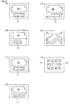
- Figs. 5 and 6 illustrate specific examples of electrode patterns disposed on dielectric layers when the switching circuit module illustrated in Fig. 2 is formed in a multilayer substrate.
- (1) to (15) represent dielectric layers of the multilayer substrate in sequence.
- (1) in Fig. 5 indicates the lowest dielectric layer
- (15) in Fig. 6 indicates the uppermost dielectric layer.
- Figs. 5 and 6 illustrate the dielectric layers (1) to (15) viewed from a bottom side (a side facing a mounting board).
- the electrode pattern illustrated in (15) in Fig. 6 is formed at an upper surface side of the dielectric layer.
- the terminals (GND, Vdd, Vc, UBAL, BAL1, BAL2) for use in mounting on a mounting board are formed on the lowest dielectric layer (1). These terminals correspond to the terminal having the same names illustrated in Fig. 2 .
- Each of the dielectric layers (1) to (5) has a cavity S.
- the high-frequency switch 21 is mounted at the front side of the dielectric layer (6) not by wire bonding but by flip-chip bonding. The high-frequency switch 21 is thus arranged in the cavity.
- Each of the dielectric layers (5) to (8) has the matching strip line SL1.
- Each of the dielectric layers (9) to (13) has an electrode of the capacitor Cs.
- Each of the dielectric layers (8) to (13) has the inductor L1 being a balance coil.
- the dielectric layer (15) has the two SAW filters F1 and F2 at its front side.
- the switching circuit module illustrated in Fig. 2 is formed on the multilayer substrate, and the dual-band switching circuit module for GSM-850 and GSM-900 is configured.
- the high-frequency switch 21 is mounted in the cavity formed in the front side of the multilayer substrate by flip-chip bonding.
- the high-frequency switch may also be arranged in a cavity formed in the underside of the multilayer substrate.
- a configuration of a triple-band switchplexer including a high-frequency switching circuit according to a second embodiment is described with reference to Figs. 7 to 9 .
- Fig. 7 is a circuit diagram of a switchplexer 101 according to the second embodiment.
- the switchplexer 101 includes a high-frequency switching circuit 42, low-pass filters LPF1 and LPF2, and SAW filters F3, F4, and F5.
- the high-frequency switching circuit 42 includes a high-frequency switch 22 and a strip line SL1 serving as a matching circuit.
- the high-frequency switch 22 selectively connects between a common input/output terminal Pc and any one of a plurality of input/output terminals P1 to P6. A control terminal and a power-supply terminal for performing this switching are omitted in Fig. 7 .
- the high-frequency switch 22 is provided with the matching strip line SL1 disposed between the common input/output terminal Pc and an antenna terminal ANT of the high-frequency switching circuit 42.
- the low-pass filter LPF1 allows a signal at a GSM-900 transmission-signal frequency band among input signals from a GSM-900 transmission-signal input terminal 900Tx to pass therethrough.
- the low-pass filter LPF2 allows a signal at a GSM-1800/1900 transmission-signal frequency band among input signals from a GSM-1800/1900 transmission-signal input terminal 1800/1900Tx to pass therethrough.
- the low-pass filter LPF1 includes strip lines GL, GLt1, and GLt2 and capacitors GCc1, GCc2, GCu1, GCu2, and GCu3.
- the low-pass filter LPF2 includes strip lines DL, DLt1, and DLt2 and capacitors DCc1, DCc2, DCu1, DGCu2, and DCu3.
- the SAW filter F3 allows a signal at a GSM-900 reception-signal frequency band with respect to signals from a reception-signal output port RX1 of the high-frequency switching circuit 42 to pass therethrough.
- the SAW filter F4 allows a signal at a GSM-1800 reception-signal frequency band with respect to signals from a reception-signal output port RX2 of the high-frequency switching circuit 42 to pass therethrough.
- the SAW filter F5 allows a signal at a GSM-1900 reception-signal frequency band with respect to signals from a reception-signal output port RX3 of the high-frequency switching circuit 42 to pass therethrough.
- a transmission and reception signal port TRX1 of the high-frequency switching circuit 42 is connected to a UMTS1 circuit.
- Figs. 8 and 9 illustrate specific examples of electrode patterns disposed on dielectric layers when the switchplexer illustrated in Fig. 7 is formed in a multilayer substrate.
- (1) to (13) represent dielectric layers of the multilayer substrate in sequence.
- (1) in Fig. 8 indicates the lowest dielectric layer
- (13) in Fig. 9 indicates the uppermost dielectric layer.
- Figs. 8 and 9 illustrate the dielectric layers (1) to (13) viewed from a bottom side (a side facing a mounting board).
- the electrode pattern illustrated in (13) in Fig. 9 is formed at an upper surface side of the dielectric layer.
- the terminals (GND, 1900Rx, 1800Rx, 900Rx, 1800/1900Tx, 900Tx, ANT, and the like) for use in mounting on a mounting board are formed on the lowest dielectric layer (1). These terminals correspond to the terminal having the same names illustrated in Fig. 7 .
- Each of the dielectric layers (2) and (11) has a ground electrode G.
- Each of the dielectric layers (3), (4), and (10) has the capacitor electrodes GCu2, GCu3, DCu2, DCu3, GCc1, GCc2, DCc1, GCu1, and DCu1.
- Each of the dielectric layers (6) to (9) has the strip lines DLt1, GLt1, GLt2, DLt2, GL, and DL.
- the dielectric layer (9) has the matching strip line SL1.
- the high-frequency switch 22 is mounted at the front side of the dielectric layer (13) not by wire bonding but by flip-chip bonding.
- the switchplexer illustrated in Fig. 7 is disposed in the multilayer substrate, and the triple-band switchplexer for GSM-900/GSM-1800/GSM-1900 is configured.
Landscapes
- Engineering & Computer Science (AREA)
- Computer Networks & Wireless Communication (AREA)
- Signal Processing (AREA)
- Physics & Mathematics (AREA)
- Acoustics & Sound (AREA)
- Transceivers (AREA)
- Electronic Switches (AREA)
- Logic Circuits (AREA)
- Waveguide Switches, Polarizers, And Phase Shifters (AREA)
Abstract
Description
- The present invention relates to high-frequency switching circuits and, in particular, to a high-frequency switching circuit including a high-frequency switch that includes a field-effect transistor (FET) switching element.
-
Patent Document 1 discloses a high-frequency switching circuit including a high-frequency switch that includes an FET switching element and that selectively connects between a common input/output terminal and one of a plurality of input/output terminals. -
Fig. 1 is a circuit diagram of a high-frequency switching circuit illustrated inPatent Document 1. The high-frequency switching circuit 14 includes an antenna terminal ANT for connection to an antenna, a reception-signal output terminal RX for connection to a receiving circuit, a transmission-signal input terminal TX for connection to a transmitting circuit, and a high-frequency switch 12 and is a circuit for switching between a transmission signal and a reception signal. - Matching circuits M1, M2, and M3 are disposed between the antenna terminal ANT and the high-
frequency switch 12, between the reception-signal output terminal RX and the high-frequency switch 12, and between the transmission-signal input terminal TX and the high-frequency switch 12, respectively. The matching circuits M1, M2, and M3 perform impedance matching between the respective terminals and the high-frequency switch 12. - The high-
frequency switch 12 is composed of a semiconductor chip made of, for example, gallium arsenide (GaAs). The chip is bonded to each of the terminals with bonding wire (gold wire). Each of the matching circuits M1, M2, and M3 is designed in consideration of an electric inductance in the bonding wire. - In the matching circuit M1 illustrated in
Fig. 1 , an inductor LL1 is the one in which an inductance being a lead to the antenna terminal ANT is represented by a symbol, a capacitor CS1 is the one in which a stray capacitance between the lead of the antenna terminal ANT and the ground is represented by a symbol, and an inductor LW1 is the one in which a bonding-wire inductance is represented by a symbol. A bulk capacitor CM1 is a metal-insulator-metal (MIM) capacitor. - Similarly, the matching circuits M2 and M3 include inductances LL2 and LL3 being lead components, stray capacitances CS2 and CS3 between the leads of the respective terminals and the ground, bonding-wire inductances LW2 and LW3, and MIM capacitors CM2 and CM3, respectively.
- [Patent Document 1] Japanese Unexamined Patent Application Publication No.
10-93302 - However, to meet a requirement for miniaturization of a high-frequency switching circuit module, it is necessary to reduce the size of a high-frequency switch, and in order to reduce its footprint, flip-chip mounting using bump connection is also necessary.
- The inductance of the bump portion in the above flip-chip mounting is significantly smaller than that in wire bonding. Thus, for the flip-chip mounting, imperfect matching occurs, and an extra line and chip inductor for achieving matching for each terminal is needed.
- Accordingly, it is an object of the present invention to provide a high-frequency switching circuit that has a small overall size and achieves impedance matching for each terminal.
- To solve the above problems, the high-frequency switching circuit according to the present invention is configured as follows:
(1) A high-frequency switching circuit comprises a high-frequency switch that includes a field-effect transistor (FET) switching element and that selectively connects between a common input/output terminal and one of a plurality of input/output terminals.
The high-frequency switching circuit comprises a matching circuit, the matching circuit being disposed between the common input/output terminal and a circuit connected to the common input/output terminal and being not disposed between the plurality of input/output terminals and a circuit connected to each of the plurality of input/output terminals. - (2) The high-frequency switch comprises a semiconductor chip and is disposed on at least one of major surfaces of a multilayer substrate by flip-chip mounting, the matching circuit includes an inductor, and the inductor is formed on a first one of the major surfaces of the multilayer substrate or inside the multilayer substrate.
- (3) The high-frequency switch comprises a semiconductor chip and is disposed on at least one of major surfaces of a multilayer substrate by flip-chip mounting, the matching circuit includes a chip inductor, the chip inductor is formed on a first one of the major surfaces of the multilayer substrate or inside the multilayer substrate.
- (4) A cavity is formed in a second one of the major surfaces of the multilayer substrate, and the semiconductor chip is arranged in the cavity.
- (5) The matching circuit is configured to correct a capacity component of the switching element being in an off state.
- (6) The circuit connected to at least one of the plurality of input/output terminals comprises a surface-acoustic-wave (SAW) filter.
- (1) The matching circuit is disposed between the common input/output terminal and the circuit connected to the common input/output terminal and is not disposed between the plurality of input/output terminals and the circuit connected to each of the plurality of input/output terminals. Accordingly, as described below, impedance matching between the common input/output terminal and all of the other input/output terminals can be achieved, the high-frequency switch can be mounted not by wire bonding, and its size can be reduced. Because the matching circuit is provided to only the common input/output terminal, the size can be further reduced correspondingly, and insertion loss can also be reduced.
- (2) The high-frequency switch comprising the semiconductor chip is disposed on at least one of the major surfaces of the multilayer substrate by flip-chip mounting, and the inductor is disposed on the multilayer substrate being a mounting board for the high-frequency switch (semiconductor chip). Accordingly, the overall size can be reduced.
- (3) The high-frequency switch comprising the semiconductor chip is disposed on at least one of the major surfaces of the multilayer substrate by flip-chip mounting, and the chip inductor being the matching circuit is mounted on the first one of the major surfaces of the multilayer substrate. Accordingly, a case where an inductor having a large inductance value is needed can be supported, and the design freedom for the matching circuit can be increased.
- (4) The cavity is formed in the second one of the major surfaces of the multilayer substrate, and the semiconductor chip being the high-frequency switch is arranged in the cavity. Accordingly, the high-frequency switching circuit having a reduced overall profile can be configured.
- (5) The matching circuit acts with the capacity of the switching element being in an off state and corrects the capacity component. Accordingly, the impedance between the common input/output terminal and a selected input/output terminal can be matched to the normal impedance, and the high-frequency switching circuit achieving impedance matching can be configured.
- (6) The circuit connected to the at least one of the plurality of input/output terminals comprises the SAW filter. Accordingly, in designing the matching circuit, impedance mismatch caused by an electric capacitance in the SAW filter can also be cancelled. This obviates the necessity to provide the SAW filter in itself with the matching circuit. The high-frequency circuit including the SAW filter can have a small overall size, and insertion loss can be reduced.
-
- [
Fig. 1] Fig. 1 illustrates a configuration of a high-frequency switching circuit illustrated inPatent Document 1. - [
Fig. 2] Fig. 2 is a circuit diagram of a high-frequency switching circuit module according to a first embodiment. - [
Fig. 3] Fig. 3 is a circuit diagram of a high-frequency switch used in the high-frequency switching circuit module. - [
Fig. 4] Fig. 4 illustrates an equivalent circuit diagram of the high-frequency switch and a matching circuit. - [
Fig. 5] Fig. 5 illustrates examples of electrode patterns disposed on dielectric layers of a multilayer substrate of the high-frequency switching circuit module according to the first embodiment. - [
Fig. 6] Fig. 6 illustrates examples of electrode patterns disposed on dielectric layers of a multilayer substrate of the high-frequency switching circuit module according to the first embodiment. - [
Fig. 7] Fig. 7 illustrates a configuration of a high-frequency switching circuit module according to a second embodiment. - [
Fig. 8] Fig. 8 illustrates examples of electrode patterns disposed on dielectric layers of a multilayer substrate of the high-frequency switching circuit module according to the second embodiment. - [
Fig. 9] Fig. 9 illustrates examples of electrode patterns disposed on dielectric layers of a multilayer substrate of the high-frequency switching circuit module according to the second embodiment. -
- 31
- matching circuit
- 21, 22
- high-frequency switch
- SL1
- matching strip line
- F1-F5
- SAW filter
- L1
- inductor
- 41, 42
- high-frequency switching circuit
- Pc
- common input/output terminal
- P1, P2
- input/output terminal
- RX, RX1,
- RX2 reception-signal output port
- 100
- switching circuit module
- 101
- high-frequency switching circuit module
- A configuration of a dual-band switching circuit module including a high-frequency switching circuit according to a first embodiment is described with reference to
Figs. 2 to 6 .
Fig. 2 is a circuit diagram of aswitching circuit module 100 including a high-frequency switching circuit according to the first embodiment. The switching circuit module is a circuit that switches between GSM-850/GSM-900 reception signals from an unbalanced terminal UBAL and outputs a selected signal in accordance with a frequency band. Theswitching circuit module 100 includes a high-frequency switching circuit 41, surface-acoustic-wave (SAW) filters F1 and F2, and an inductor L1. - The high-
frequency switching circuit 41 includes a high-frequency switch 21 and amatching circuit 31. The high-frequency switch 21 includes a field-effect transistor (FET) switching element and selectively connects between a common input/output terminal Pc and one of two input/output terminals P1 and P2. The matchingcircuit 31 includes a matching strip line SL1 and is connected between the common input/output terminal Pc of the high-frequency switch 21 and the unbalanced terminal UBAL. - A first reception-signal output port RX1 of the high-frequency switching circuit 41 (the first input/output terminal P1 of the high-frequency switch 21) is connected to an unbalanced terminal of the first SAW filter F1. The first SAW filter F1 allows a GSM-850 reception signal to pass therethrough. Similarly, a second reception-signal output port RX2 (the second input/output terminal P2 of the high-frequency switch 21) is connected to an unbalanced terminal of the second SAW filter F2. The second SAW filter F2 allows a GSM-900 reception signal to pass therethrough.
- A balanced terminal of the first SAW filter F1 and that of the second SAW filter F2 are mutually connected, and an inductor L1 serving as a balance coil is connected between balanced terminals BAL1 and BAL2.
- A power supply voltage input into a power-supply terminal Vdd of the high-
frequency switching circuit 41 is applied to the high-frequency switch 21. A control voltage input into a control terminal Vc is applied to the high-frequency switch 21. -
Fig. 3 is a circuit diagram that illustrates a specific configuration of the high-frequency switch 21 illustrated inFig. 2 . An FET Q1 is connected in series and an FET Q2 is connected in shunt between the common input/output terminal Pc and the first input/output terminal P1. The FET Q1 and Q2 have gates to which control voltages V1 and V2 are applied through resistors R1 and R2, respectively. Similarly, an FET Q3 is connected in series and an FET Q4 is connected in shunt between the common input/output terminal Pc and the second input/output terminal P2. The FET Q3 and Q4 have gates to which control voltages V3 and V4 are applied through resistors R3 and R4, respectively.
InFig. 3 , the control voltages V1 to V4 are applied such that, when the FET Q1 and Q4 are in an on state, the FET Q2 and Q3 are in an off state, and in contrast, when the FET Q2 and Q3 are in an on state, the FET Q1 and Q4 are in an off state. -
Fig. 4 illustrates equivalent circuit diagrams when the FET Q1 and Q4 are in an on state and the FET Q2 and Q3 are in an off state in the high-frequency switch 21 illustrated inFig. 3 . The FETs in an on state are represented by the resistors R1 and R4, and the FETs in an off state are represented by capacitors C2 and C3. Accordingly, this state indicates a parallel circuit of a series circuit of R1 and C2 and a series circuit of C3 and R4 and can be represented by a circuit constituting a series circuit of a resistor R0 and a capacitor C0 between the common input/output terminal Pc and the ground, as illustrated inFig. 4(B) . - The same applies to a situation where the FET Q1 and Q4 illustrated in
Fig. 3 are in an off state and the FET Q2 and Q3 are in an on state. - The existence of an input/output terminal that is not selected allows the non-selected input/output terminal (port) to act as a capacitor, thus causing a displacement of the impedance between the common input/output terminal and a selected input/output terminal from a normal impedance (50Ω). To correct the capacitance C0 disposed in parallel between the line and the ground in this circuit and make the impedance viewed from the common input/output terminal Pc to the high-
frequency switch 21 equal to the normal impedance, the matchingcircuit 31 is provided, as illustrated inFig. 4(C) . The matchingcircuit 31 illustrated inFig. 2 is a circuit determined in this way. - The above matching circuit may also include the matching strip line SL1 and a capacitor Cm connected in shunt with the signal line. The provision of the capacitor Cm allows the impedance to be determined by the inductance of the strip line SL1 and the capacitance of the capacitor Cm. Accordingly, the design freedom for the matching circuit can be improved.
- Determining the impedance of the matching
circuit 31 so as to cancel an impedance mismatch caused by an electric capacitance in the SAW filters F1 and F2 in designing the high-frequency switch 21 obviates the necessity to provide each of the SAW filters F1 and F2 in itself with the matching circuit. This leads to a small overall size of the high-frequency circuit including the SAW filters and a reduction in insertion loss. -
Figs. 5 and6 illustrate specific examples of electrode patterns disposed on dielectric layers when the switching circuit module illustrated inFig. 2 is formed in a multilayer substrate. - In
Figs. 5 and6 , (1) to (15) represent dielectric layers of the multilayer substrate in sequence. (1) inFig. 5 indicates the lowest dielectric layer, and (15) inFig. 6 indicates the uppermost dielectric layer.Figs. 5 and6 illustrate the dielectric layers (1) to (15) viewed from a bottom side (a side facing a mounting board). The electrode pattern illustrated in (15) inFig. 6 is formed at an upper surface side of the dielectric layer. - The terminals (GND, Vdd, Vc, UBAL, BAL1, BAL2) for use in mounting on a mounting board are formed on the lowest dielectric layer (1). These terminals correspond to the terminal having the same names illustrated in
Fig. 2 . - Each of the dielectric layers (1) to (5) has a cavity S. The high-
frequency switch 21 is mounted at the front side of the dielectric layer (6) not by wire bonding but by flip-chip bonding. The high-frequency switch 21 is thus arranged in the cavity. - Each of the dielectric layers (5) to (8) has the matching strip line SL1. Each of the dielectric layers (9) to (13) has an electrode of the capacitor Cs.
Each of the dielectric layers (8) to (13) has the inductor L1 being a balance coil.
The dielectric layer (15) has the two SAW filters F1 and F2 at its front side. - In such a way, the switching circuit module illustrated in
Fig. 2 is formed on the multilayer substrate, and the dual-band switching circuit module for GSM-850 and GSM-900 is configured. - In the first embodiment, the high-
frequency switch 21 is mounted in the cavity formed in the front side of the multilayer substrate by flip-chip bonding. However, the high-frequency switch may also be arranged in a cavity formed in the underside of the multilayer substrate. - A configuration of a triple-band switchplexer including a high-frequency switching circuit according to a second embodiment is described with reference to
Figs. 7 to 9 . -
Fig. 7 is a circuit diagram of aswitchplexer 101 according to the second embodiment. Theswitchplexer 101 includes a high-frequency switching circuit 42, low-pass filters LPF1 and LPF2, and SAW filters F3, F4, and F5. - The high-
frequency switching circuit 42 includes a high-frequency switch 22 and a strip line SL1 serving as a matching circuit. The high-frequency switch 22 selectively connects between a common input/output terminal Pc and any one of a plurality of input/output terminals P1 to P6. A control terminal and a power-supply terminal for performing this switching are omitted inFig. 7 . The high-frequency switch 22 is provided with the matching strip line SL1 disposed between the common input/output terminal Pc and an antenna terminal ANT of the high-frequency switching circuit 42. - The low-pass filter LPF1 allows a signal at a GSM-900 transmission-signal frequency band among input signals from a GSM-900 transmission-signal input terminal 900Tx to pass therethrough. Similarly, the low-pass filter LPF2 allows a signal at a GSM-1800/1900 transmission-signal frequency band among input signals from a GSM-1800/1900 transmission-
signal input terminal 1800/1900Tx to pass therethrough. - The low-pass filter LPF1 includes strip lines GL, GLt1, and GLt2 and capacitors GCc1, GCc2, GCu1, GCu2, and GCu3. Similarly, the low-pass filter LPF2 includes strip lines DL, DLt1, and DLt2 and capacitors DCc1, DCc2, DCu1, DGCu2, and DCu3.
- The SAW filter F3 allows a signal at a GSM-900 reception-signal frequency band with respect to signals from a reception-signal output port RX1 of the high-
frequency switching circuit 42 to pass therethrough. The SAW filter F4 allows a signal at a GSM-1800 reception-signal frequency band with respect to signals from a reception-signal output port RX2 of the high-frequency switching circuit 42 to pass therethrough. Similarly, the SAW filter F5 allows a signal at a GSM-1900 reception-signal frequency band with respect to signals from a reception-signal output port RX3 of the high-frequency switching circuit 42 to pass therethrough. - A transmission and reception signal port TRX1 of the high-
frequency switching circuit 42 is connected to a UMTS1 circuit. -
Figs. 8 and9 illustrate specific examples of electrode patterns disposed on dielectric layers when the switchplexer illustrated inFig. 7 is formed in a multilayer substrate. - In
Figs. 8 and9 , (1) to (13) represent dielectric layers of the multilayer substrate in sequence. (1) inFig. 8 indicates the lowest dielectric layer, and (13) inFig. 9 indicates the uppermost dielectric layer.Figs. 8 and9 illustrate the dielectric layers (1) to (13) viewed from a bottom side (a side facing a mounting board). The electrode pattern illustrated in (13) inFig. 9 is formed at an upper surface side of the dielectric layer. - The terminals (GND, 1900Rx, 1800Rx, 900Rx, 1800/1900Tx, 900Tx, ANT, and the like) for use in mounting on a mounting board are formed on the lowest dielectric layer (1). These terminals correspond to the terminal having the same names illustrated in
Fig. 7 . - Each of the dielectric layers (2) and (11) has a ground electrode G.
Each of the dielectric layers (3), (4), and (10) has the capacitor electrodes GCu2, GCu3, DCu2, DCu3, GCc1, GCc2, DCc1, GCu1, and DCu1. - Each of the dielectric layers (6) to (9) has the strip lines DLt1, GLt1, GLt2, DLt2, GL, and DL.
The dielectric layer (9) has the matching strip line SL1.
The high-frequency switch 22 is mounted at the front side of the dielectric layer (13) not by wire bonding but by flip-chip bonding. - In such a way, the switchplexer illustrated in
Fig. 7 is disposed in the multilayer substrate, and the triple-band switchplexer for GSM-900/GSM-1800/GSM-1900 is configured.
Claims (8)
- A high-frequency switching circuit module comprising a high-frequency switch that includes a field-effect transistor (FET) switching element and that selectively connects between a common input/output terminal and one of a plurality of input/output terminals,
the high-frequency switching circuit module comprising a matching circuit, wherein the matching circuit is disposed between the common input/output terminal and a circuit connected to the common input/output terminal and is not disposed between the plurality of input/output terminals and a circuit connected to each of the plurality of input/output terminals. - The high-frequency switching circuit module according to Claim 1, wherein the matching circuit comprises an inductor arranged in series between the common input/output terminal and the circuit connected to the common input/output terminal.
- The high-frequency switching circuit module according to Claim 2, wherein the matching circuit further includes a capacitor connected in shunt.
- The high-frequency switching circuit module according to any one of Claims 1 to 3, wherein the high-frequency switch comprises a semiconductor chip and is disposed on at least one of major surfaces of a multilayer substrate by flip-chip mounting, the matching circuit includes an inductor, and the inductor is formed on a first one of the major surfaces of the multilayer substrate or inside the multilayer substrate.
- The high-frequency switching circuit module according to any one of Claims 1 to 3, wherein the high-frequency switch comprises a semiconductor chip and is disposed on at least one of major surfaces of a multilayer substrate by flip-chip mounting, the matching circuit includes a chip inductor, the chip inductor is formed on a first one of the major surfaces of the multilayer substrate or inside the multilayer substrate.
- The high-frequency switching circuit module according to Claim 4 or 5, wherein a cavity is formed in a second one of the major surfaces of the multilayer substrate, and the semiconductor chip is arranged in the cavity.
- The high-frequency switching circuit module according to any one of Claims 1 to 6, wherein the matching circuit is configured to correct an electric capacitance of the switching element being in an off state.
- The high-frequency switching circuit module according to any one of Claims 1 to 5, wherein the circuit connected to at least one of the plurality of input/output terminals comprises a surface-acoustic-wave (SAW) filter.
Applications Claiming Priority (2)
| Application Number | Priority Date | Filing Date | Title |
|---|---|---|---|
| JP2006345058 | 2006-12-21 | ||
| PCT/JP2007/073303 WO2008075551A1 (en) | 2006-12-21 | 2007-12-03 | High-frequency switch circuit |
Publications (3)
| Publication Number | Publication Date |
|---|---|
| EP2096766A1 true EP2096766A1 (en) | 2009-09-02 |
| EP2096766A4 EP2096766A4 (en) | 2010-08-18 |
| EP2096766B1 EP2096766B1 (en) | 2016-08-17 |
Family
ID=39536185
Family Applications (1)
| Application Number | Title | Priority Date | Filing Date |
|---|---|---|---|
| EP07832923.2A Not-in-force EP2096766B1 (en) | 2006-12-21 | 2007-12-03 | High-frequency switch circuit |
Country Status (7)
| Country | Link |
|---|---|
| US (1) | US7812687B2 (en) |
| EP (1) | EP2096766B1 (en) |
| JP (1) | JP4433087B2 (en) |
| KR (1) | KR101048337B1 (en) |
| CN (1) | CN101573881B (en) |
| TW (1) | TW200832802A (en) |
| WO (1) | WO2008075551A1 (en) |
Families Citing this family (13)
| Publication number | Priority date | Publication date | Assignee | Title |
|---|---|---|---|---|
| KR101126683B1 (en) * | 2010-05-17 | 2012-03-16 | 주식회사 아이엠텍 | Multi-band Antenna Switching Module |
| CN103026622B (en) * | 2010-07-27 | 2015-06-17 | 株式会社村田制作所 | High-frequency module |
| US9136838B2 (en) * | 2010-09-21 | 2015-09-15 | Dsp Group Ltd. | RF switch implementation in CMOS process |
| US20130252562A1 (en) * | 2010-09-21 | 2013-09-26 | Dsp Group, Ltd. | High power high isolation low current cmos rf switch |
| JP5304811B2 (en) * | 2011-02-14 | 2013-10-02 | 株式会社村田製作所 | High frequency module |
| US9287062B2 (en) * | 2012-05-02 | 2016-03-15 | National Instruments Corporation | Magnetic switching system |
| DE102013109463A1 (en) * | 2013-08-30 | 2015-03-05 | Endress + Hauser Gmbh + Co. Kg | Method for optimizing the impedance of a connecting element |
| US9641201B2 (en) * | 2014-04-29 | 2017-05-02 | Infineon Technologies Ag | System and method for a radio frequency integrated circuit |
| WO2016133028A1 (en) | 2015-02-20 | 2016-08-25 | 株式会社村田製作所 | High-frequency filter, high-frequency front-end circuit, communication device, and method for designing high-frequency filter |
| JP6520857B2 (en) | 2016-08-05 | 2019-05-29 | 株式会社村田製作所 | High frequency module and method of manufacturing elastic wave filter |
| US10320363B2 (en) | 2016-08-05 | 2019-06-11 | Murata Manufacturing Co., Ltd. | High-frequency module |
| US10075160B2 (en) * | 2016-08-10 | 2018-09-11 | Murata Manufacturing Co., Ltd. | Switch circuit, radio-frequency module, and communication device |
| WO2019065863A1 (en) * | 2017-09-29 | 2019-04-04 | 株式会社村田製作所 | Multiplexer, high-frequency front-end circuit, and communication device |
Family Cites Families (20)
| Publication number | Priority date | Publication date | Assignee | Title |
|---|---|---|---|---|
| JP3215292B2 (en) | 1995-06-05 | 2001-10-02 | 松下電器産業株式会社 | Semiconductor device |
| JP3029119U (en) | 1996-03-19 | 1996-09-27 | 株式会社スギ電子 | Wireless card |
| JP3798855B2 (en) | 1996-09-11 | 2006-07-19 | 株式会社村田製作所 | Signal selector switch |
| JPH1093471A (en) | 1996-09-11 | 1998-04-10 | Murata Mfg Co Ltd | Signal changeover switch |
| JP3628562B2 (en) | 1999-09-16 | 2005-03-16 | 三菱電機株式会社 | transceiver |
| JP2001189605A (en) * | 1999-10-21 | 2001-07-10 | Matsushita Electric Ind Co Ltd | Ceramic multilayer RF device |
| US6456172B1 (en) * | 1999-10-21 | 2002-09-24 | Matsushita Electric Industrial Co., Ltd. | Multilayered ceramic RF device |
| KR100875947B1 (en) | 2000-03-15 | 2008-12-26 | 히타치 긴조쿠 가부시키가이샤 | High frequency composite parts and wireless communication device using the same |
| JP2003032001A (en) * | 2001-07-13 | 2003-01-31 | Murata Mfg Co Ltd | Compound high frequency switch, high frequency module and communication device |
| US7057472B2 (en) * | 2001-08-10 | 2006-06-06 | Hitachi Metals, Ltd. | Bypass filter, multi-band antenna switch circuit, and layered module composite part and communication device using them |
| JP2003133882A (en) | 2001-08-16 | 2003-05-09 | Murata Mfg Co Ltd | Impedance matching element |
| CN1327733C (en) * | 2002-08-08 | 2007-07-18 | 松下电器产业株式会社 | High frequency element |
| JP2004187215A (en) | 2002-12-06 | 2004-07-02 | Hitachi Metals Ltd | High frequency switch circuit |
| JP2005020140A (en) * | 2003-06-24 | 2005-01-20 | Ngk Spark Plug Co Ltd | ANTENNA SWITCH MODULE AND WIRELESS TELEPHONE COMMUNICATION DEVICE USING THE SAME |
| JP2005045345A (en) | 2003-07-23 | 2005-02-17 | Murata Mfg Co Ltd | High frequency module |
| JP2005064780A (en) | 2003-08-11 | 2005-03-10 | Fdk Corp | High frequency switch circuit |
| US7596357B2 (en) * | 2004-02-27 | 2009-09-29 | Kyocera Corporation | High-frequency switching circuit, high-frequency module, and wireless communications device |
| JP4465286B2 (en) | 2004-02-27 | 2010-05-19 | 京セラ株式会社 | High frequency selection circuit, high frequency module, and wireless communication device |
| ATE417410T1 (en) * | 2004-11-25 | 2008-12-15 | Murata Manufacturing Co | HIGH FREQUENCY SWITCHING MODULE |
| JP2006157423A (en) | 2004-11-29 | 2006-06-15 | Matsushita Electric Ind Co Ltd | High frequency switch circuit |
-
2007
- 2007-12-03 CN CN2007800474294A patent/CN101573881B/en not_active Expired - Fee Related
- 2007-12-03 WO PCT/JP2007/073303 patent/WO2008075551A1/en not_active Ceased
- 2007-12-03 JP JP2008550085A patent/JP4433087B2/en not_active Expired - Fee Related
- 2007-12-03 EP EP07832923.2A patent/EP2096766B1/en not_active Not-in-force
- 2007-12-03 KR KR1020097010287A patent/KR101048337B1/en not_active Expired - Fee Related
- 2007-12-06 TW TW096146451A patent/TW200832802A/en not_active IP Right Cessation
-
2009
- 2009-06-15 US US12/484,272 patent/US7812687B2/en active Active
Non-Patent Citations (2)
| Title |
|---|
| No further relevant documents disclosed * |
| See also references of WO2008075551A1 * |
Also Published As
| Publication number | Publication date |
|---|---|
| CN101573881A (en) | 2009-11-04 |
| KR101048337B1 (en) | 2011-07-14 |
| US20090243703A1 (en) | 2009-10-01 |
| EP2096766B1 (en) | 2016-08-17 |
| TW200832802A (en) | 2008-08-01 |
| WO2008075551A1 (en) | 2008-06-26 |
| JPWO2008075551A1 (en) | 2010-04-08 |
| KR20090080092A (en) | 2009-07-23 |
| EP2096766A4 (en) | 2010-08-18 |
| JP4433087B2 (en) | 2010-03-17 |
| TWI358850B (en) | 2012-02-21 |
| US7812687B2 (en) | 2010-10-12 |
| CN101573881B (en) | 2013-04-17 |
Similar Documents
| Publication | Publication Date | Title |
|---|---|---|
| EP2096766A1 (en) | High-frequency switch circuit | |
| EP1775847B1 (en) | High frequency composite component | |
| CN100555861C (en) | High frequency selection circuit, high frequency module and wireless communication device | |
| EP1261143B1 (en) | Transceiver front end module | |
| CN102138285B (en) | High-frequency switch module | |
| EP1981173A1 (en) | Composite high-frequency components and mobile communication apparatus | |
| US11601096B2 (en) | Power amplifier module, frontend circuit, and communication device | |
| CN100525127C (en) | Electric switch module, switch module arrangement, mobile radio equipment with the switch module and mobile radio equipment with the switch module arrangement | |
| EP2019494A1 (en) | High-frequency switch module | |
| US20220385330A1 (en) | Transceiver having radio-frequency front-end circuit, dedicated radio-frequency front-end circuit, and switchable matching circuit integrated in same chip | |
| US20040264095A1 (en) | Circuit arrangement, switching module comprising said circuit arrangement and use of said switching module | |
| US7904031B2 (en) | High-frequency module for transmitting and receiving transmission-reception signals of at least three communication systems using a single antenna | |
| JP2006129419A (en) | High frequency selection circuit, high frequency module, and wireless communication device | |
| US20090075604A1 (en) | High frequency module | |
| US7848727B2 (en) | Integrated radio frequency module | |
| US7449977B2 (en) | Circuit having isolated transmitting and receiving paths | |
| US11729903B2 (en) | Radio frequency module and communication device | |
| JP2004146916A (en) | High frequency switch circuit and high frequency switch module | |
| US12451921B2 (en) | Radio-frequency module and communication apparatus | |
| CN117895205A (en) | Directional coupler, high frequency module and communication device | |
| KR20040076684A (en) | Manufacturing method of dual band front end module | |
| KR20040107992A (en) | Dual Band Front End Module |
Legal Events
| Date | Code | Title | Description |
|---|---|---|---|
| PUAI | Public reference made under article 153(3) epc to a published international application that has entered the european phase |
Free format text: ORIGINAL CODE: 0009012 |
|
| 17P | Request for examination filed |
Effective date: 20090525 |
|
| AK | Designated contracting states |
Kind code of ref document: A1 Designated state(s): AT BE BG CH CY CZ DE DK EE ES FI FR GB GR HU IE IS IT LI LT LU LV MC MT NL PL PT RO SE SI SK TR |
|
| DAX | Request for extension of the european patent (deleted) | ||
| A4 | Supplementary search report drawn up and despatched |
Effective date: 20100716 |
|
| REG | Reference to a national code |
Ref country code: DE Ref legal event code: R079 Ref document number: 602007047532 Country of ref document: DE Free format text: PREVIOUS MAIN CLASS: H04B0001400000 Ipc: H04B0001440000 |
|
| GRAP | Despatch of communication of intention to grant a patent |
Free format text: ORIGINAL CODE: EPIDOSNIGR1 |
|
| RIC1 | Information provided on ipc code assigned before grant |
Ipc: H04B 1/44 20060101AFI20160226BHEP Ipc: H03H 9/72 20060101ALI20160226BHEP |
|
| INTG | Intention to grant announced |
Effective date: 20160314 |
|
| RIN1 | Information on inventor provided before grant (corrected) |
Inventor name: FURUTANI, KOJI |
|
| GRAS | Grant fee paid |
Free format text: ORIGINAL CODE: EPIDOSNIGR3 |
|
| GRAA | (expected) grant |
Free format text: ORIGINAL CODE: 0009210 |
|
| AK | Designated contracting states |
Kind code of ref document: B1 Designated state(s): AT BE BG CH CY CZ DE DK EE ES FI FR GB GR HU IE IS IT LI LT LU LV MC MT NL PL PT RO SE SI SK TR |
|
| REG | Reference to a national code |
Ref country code: GB Ref legal event code: FG4D |
|
| REG | Reference to a national code |
Ref country code: CH Ref legal event code: EP |
|
| REG | Reference to a national code |
Ref country code: IE Ref legal event code: FG4D |
|
| REG | Reference to a national code |
Ref country code: AT Ref legal event code: REF Ref document number: 821925 Country of ref document: AT Kind code of ref document: T Effective date: 20160915 |
|
| REG | Reference to a national code |
Ref country code: DE Ref legal event code: R096 Ref document number: 602007047532 Country of ref document: DE |
|
| REG | Reference to a national code |
Ref country code: NL Ref legal event code: MP Effective date: 20160817 |
|
| REG | Reference to a national code |
Ref country code: LT Ref legal event code: MG4D |
|
| REG | Reference to a national code |
Ref country code: AT Ref legal event code: MK05 Ref document number: 821925 Country of ref document: AT Kind code of ref document: T Effective date: 20160817 |
|
| PG25 | Lapsed in a contracting state [announced via postgrant information from national office to epo] |
Ref country code: NL Free format text: LAPSE BECAUSE OF FAILURE TO SUBMIT A TRANSLATION OF THE DESCRIPTION OR TO PAY THE FEE WITHIN THE PRESCRIBED TIME-LIMIT Effective date: 20160817 Ref country code: LT Free format text: LAPSE BECAUSE OF FAILURE TO SUBMIT A TRANSLATION OF THE DESCRIPTION OR TO PAY THE FEE WITHIN THE PRESCRIBED TIME-LIMIT Effective date: 20160817 Ref country code: FI Free format text: LAPSE BECAUSE OF FAILURE TO SUBMIT A TRANSLATION OF THE DESCRIPTION OR TO PAY THE FEE WITHIN THE PRESCRIBED TIME-LIMIT Effective date: 20160817 Ref country code: IT Free format text: LAPSE BECAUSE OF FAILURE TO SUBMIT A TRANSLATION OF THE DESCRIPTION OR TO PAY THE FEE WITHIN THE PRESCRIBED TIME-LIMIT Effective date: 20160817 |
|
| PG25 | Lapsed in a contracting state [announced via postgrant information from national office to epo] |
Ref country code: PL Free format text: LAPSE BECAUSE OF FAILURE TO SUBMIT A TRANSLATION OF THE DESCRIPTION OR TO PAY THE FEE WITHIN THE PRESCRIBED TIME-LIMIT Effective date: 20160817 Ref country code: ES Free format text: LAPSE BECAUSE OF FAILURE TO SUBMIT A TRANSLATION OF THE DESCRIPTION OR TO PAY THE FEE WITHIN THE PRESCRIBED TIME-LIMIT Effective date: 20160817 Ref country code: AT Free format text: LAPSE BECAUSE OF FAILURE TO SUBMIT A TRANSLATION OF THE DESCRIPTION OR TO PAY THE FEE WITHIN THE PRESCRIBED TIME-LIMIT Effective date: 20160817 Ref country code: SE Free format text: LAPSE BECAUSE OF FAILURE TO SUBMIT A TRANSLATION OF THE DESCRIPTION OR TO PAY THE FEE WITHIN THE PRESCRIBED TIME-LIMIT Effective date: 20160817 Ref country code: LV Free format text: LAPSE BECAUSE OF FAILURE TO SUBMIT A TRANSLATION OF THE DESCRIPTION OR TO PAY THE FEE WITHIN THE PRESCRIBED TIME-LIMIT Effective date: 20160817 Ref country code: PT Free format text: LAPSE BECAUSE OF FAILURE TO SUBMIT A TRANSLATION OF THE DESCRIPTION OR TO PAY THE FEE WITHIN THE PRESCRIBED TIME-LIMIT Effective date: 20161219 Ref country code: GR Free format text: LAPSE BECAUSE OF FAILURE TO SUBMIT A TRANSLATION OF THE DESCRIPTION OR TO PAY THE FEE WITHIN THE PRESCRIBED TIME-LIMIT Effective date: 20161118 |
|
| PG25 | Lapsed in a contracting state [announced via postgrant information from national office to epo] |
Ref country code: EE Free format text: LAPSE BECAUSE OF FAILURE TO SUBMIT A TRANSLATION OF THE DESCRIPTION OR TO PAY THE FEE WITHIN THE PRESCRIBED TIME-LIMIT Effective date: 20160817 Ref country code: RO Free format text: LAPSE BECAUSE OF FAILURE TO SUBMIT A TRANSLATION OF THE DESCRIPTION OR TO PAY THE FEE WITHIN THE PRESCRIBED TIME-LIMIT Effective date: 20160817 |
|
| REG | Reference to a national code |
Ref country code: DE Ref legal event code: R097 Ref document number: 602007047532 Country of ref document: DE |
|
| PG25 | Lapsed in a contracting state [announced via postgrant information from national office to epo] |
Ref country code: SK Free format text: LAPSE BECAUSE OF FAILURE TO SUBMIT A TRANSLATION OF THE DESCRIPTION OR TO PAY THE FEE WITHIN THE PRESCRIBED TIME-LIMIT Effective date: 20160817 Ref country code: BG Free format text: LAPSE BECAUSE OF FAILURE TO SUBMIT A TRANSLATION OF THE DESCRIPTION OR TO PAY THE FEE WITHIN THE PRESCRIBED TIME-LIMIT Effective date: 20161117 Ref country code: DK Free format text: LAPSE BECAUSE OF FAILURE TO SUBMIT A TRANSLATION OF THE DESCRIPTION OR TO PAY THE FEE WITHIN THE PRESCRIBED TIME-LIMIT Effective date: 20160817 Ref country code: BE Free format text: LAPSE BECAUSE OF FAILURE TO SUBMIT A TRANSLATION OF THE DESCRIPTION OR TO PAY THE FEE WITHIN THE PRESCRIBED TIME-LIMIT Effective date: 20160817 Ref country code: CZ Free format text: LAPSE BECAUSE OF FAILURE TO SUBMIT A TRANSLATION OF THE DESCRIPTION OR TO PAY THE FEE WITHIN THE PRESCRIBED TIME-LIMIT Effective date: 20160817 |
|
| PLBE | No opposition filed within time limit |
Free format text: ORIGINAL CODE: 0009261 |
|
| STAA | Information on the status of an ep patent application or granted ep patent |
Free format text: STATUS: NO OPPOSITION FILED WITHIN TIME LIMIT |
|
| 26N | No opposition filed |
Effective date: 20170518 |
|
| REG | Reference to a national code |
Ref country code: CH Ref legal event code: PL |
|
| GBPC | Gb: european patent ceased through non-payment of renewal fee |
Effective date: 20161203 |
|
| PG25 | Lapsed in a contracting state [announced via postgrant information from national office to epo] |
Ref country code: SI Free format text: LAPSE BECAUSE OF FAILURE TO SUBMIT A TRANSLATION OF THE DESCRIPTION OR TO PAY THE FEE WITHIN THE PRESCRIBED TIME-LIMIT Effective date: 20160817 |
|
| PG25 | Lapsed in a contracting state [announced via postgrant information from national office to epo] |
Ref country code: MC Free format text: LAPSE BECAUSE OF FAILURE TO SUBMIT A TRANSLATION OF THE DESCRIPTION OR TO PAY THE FEE WITHIN THE PRESCRIBED TIME-LIMIT Effective date: 20160817 |
|
| REG | Reference to a national code |
Ref country code: FR Ref legal event code: ST Effective date: 20170831 |
|
| REG | Reference to a national code |
Ref country code: IE Ref legal event code: MM4A |
|
| PG25 | Lapsed in a contracting state [announced via postgrant information from national office to epo] |
Ref country code: CH Free format text: LAPSE BECAUSE OF NON-PAYMENT OF DUE FEES Effective date: 20161231 Ref country code: FR Free format text: LAPSE BECAUSE OF NON-PAYMENT OF DUE FEES Effective date: 20170102 Ref country code: LI Free format text: LAPSE BECAUSE OF NON-PAYMENT OF DUE FEES Effective date: 20161231 Ref country code: LU Free format text: LAPSE BECAUSE OF NON-PAYMENT OF DUE FEES Effective date: 20161203 |
|
| PG25 | Lapsed in a contracting state [announced via postgrant information from national office to epo] |
Ref country code: IE Free format text: LAPSE BECAUSE OF NON-PAYMENT OF DUE FEES Effective date: 20161203 Ref country code: GB Free format text: LAPSE BECAUSE OF NON-PAYMENT OF DUE FEES Effective date: 20161203 |
|
| PG25 | Lapsed in a contracting state [announced via postgrant information from national office to epo] |
Ref country code: CY Free format text: LAPSE BECAUSE OF FAILURE TO SUBMIT A TRANSLATION OF THE DESCRIPTION OR TO PAY THE FEE WITHIN THE PRESCRIBED TIME-LIMIT Effective date: 20160817 Ref country code: HU Free format text: LAPSE BECAUSE OF FAILURE TO SUBMIT A TRANSLATION OF THE DESCRIPTION OR TO PAY THE FEE WITHIN THE PRESCRIBED TIME-LIMIT; INVALID AB INITIO Effective date: 20071203 |
|
| PG25 | Lapsed in a contracting state [announced via postgrant information from national office to epo] |
Ref country code: TR Free format text: LAPSE BECAUSE OF FAILURE TO SUBMIT A TRANSLATION OF THE DESCRIPTION OR TO PAY THE FEE WITHIN THE PRESCRIBED TIME-LIMIT Effective date: 20160817 Ref country code: IS Free format text: LAPSE BECAUSE OF FAILURE TO SUBMIT A TRANSLATION OF THE DESCRIPTION OR TO PAY THE FEE WITHIN THE PRESCRIBED TIME-LIMIT Effective date: 20160817 |
|
| PG25 | Lapsed in a contracting state [announced via postgrant information from national office to epo] |
Ref country code: MT Free format text: LAPSE BECAUSE OF NON-PAYMENT OF DUE FEES Effective date: 20161203 |
|
| PGFP | Annual fee paid to national office [announced via postgrant information from national office to epo] |
Ref country code: DE Payment date: 20211210 Year of fee payment: 15 |
|
| REG | Reference to a national code |
Ref country code: DE Ref legal event code: R119 Ref document number: 602007047532 Country of ref document: DE |
|
| PG25 | Lapsed in a contracting state [announced via postgrant information from national office to epo] |
Ref country code: DE Free format text: LAPSE BECAUSE OF NON-PAYMENT OF DUE FEES Effective date: 20230701 |