EP2093797A1 - Procédé d'alignement de deux substrats par des microbobines - Google Patents
Procédé d'alignement de deux substrats par des microbobines Download PDFInfo
- Publication number
- EP2093797A1 EP2093797A1 EP09354005A EP09354005A EP2093797A1 EP 2093797 A1 EP2093797 A1 EP 2093797A1 EP 09354005 A EP09354005 A EP 09354005A EP 09354005 A EP09354005 A EP 09354005A EP 2093797 A1 EP2093797 A1 EP 2093797A1
- Authority
- EP
- European Patent Office
- Prior art keywords
- microbubines
- alignment
- substrates
- substrate
- process according
- Prior art date
- Legal status (The legal status is an assumption and is not a legal conclusion. Google has not performed a legal analysis and makes no representation as to the accuracy of the status listed.)
- Granted
Links
Images

Classifications
-
- B—PERFORMING OPERATIONS; TRANSPORTING
- B81—MICROSTRUCTURAL TECHNOLOGY
- B81C—PROCESSES OR APPARATUS SPECIALLY ADAPTED FOR THE MANUFACTURE OR TREATMENT OF MICROSTRUCTURAL DEVICES OR SYSTEMS
- B81C3/00—Assembling of devices or systems from individually processed components
- B81C3/002—Aligning microparts
- B81C3/004—Active alignment, i.e. moving the elements in response to the detected position of the elements using internal or external actuators
-
- H—ELECTRICITY
- H10—SEMICONDUCTOR DEVICES; ELECTRIC SOLID-STATE DEVICES NOT OTHERWISE PROVIDED FOR
- H10W—GENERIC PACKAGES, INTERCONNECTIONS, CONNECTORS OR OTHER CONSTRUCTIONAL DETAILS OF DEVICES COVERED BY CLASS H10
- H10W44/00—Electrical arrangements for controlling or matching impedance
- H10W44/501—Inductive arrangements
-
- H—ELECTRICITY
- H10—SEMICONDUCTOR DEVICES; ELECTRIC SOLID-STATE DEVICES NOT OTHERWISE PROVIDED FOR
- H10W—GENERIC PACKAGES, INTERCONNECTIONS, CONNECTORS OR OTHER CONSTRUCTIONAL DETAILS OF DEVICES COVERED BY CLASS H10
- H10W90/00—Package configurations
-
- H—ELECTRICITY
- H10—SEMICONDUCTOR DEVICES; ELECTRIC SOLID-STATE DEVICES NOT OTHERWISE PROVIDED FOR
- H10W—GENERIC PACKAGES, INTERCONNECTIONS, CONNECTORS OR OTHER CONSTRUCTIONAL DETAILS OF DEVICES COVERED BY CLASS H10
- H10W90/00—Package configurations
- H10W90/20—Configurations of stacked chips
- H10W90/293—Configurations of stacked chips characterised by non-galvanic coupling between the chips, e.g. capacitive coupling
-
- B—PERFORMING OPERATIONS; TRANSPORTING
- B81—MICROSTRUCTURAL TECHNOLOGY
- B81B—MICROSTRUCTURAL DEVICES OR SYSTEMS, e.g. MICROMECHANICAL DEVICES
- B81B2207/00—Microstructural systems or auxiliary parts thereof
- B81B2207/01—Microstructural systems or auxiliary parts thereof comprising a micromechanical device connected to control or processing electronics, i.e. Smart-MEMS
- B81B2207/017—Smart-MEMS not provided for in B81B2207/012 - B81B2207/015
-
- B—PERFORMING OPERATIONS; TRANSPORTING
- B81—MICROSTRUCTURAL TECHNOLOGY
- B81C—PROCESSES OR APPARATUS SPECIALLY ADAPTED FOR THE MANUFACTURE OR TREATMENT OF MICROSTRUCTURAL DEVICES OR SYSTEMS
- B81C2201/00—Manufacture or treatment of microstructural devices or systems
- B81C2201/01—Manufacture or treatment of microstructural devices or systems in or on a substrate
- B81C2201/0174—Manufacture or treatment of microstructural devices or systems in or on a substrate for making multi-layered devices, film deposition or growing
- B81C2201/019—Bonding or gluing multiple substrate layers
-
- B—PERFORMING OPERATIONS; TRANSPORTING
- B81—MICROSTRUCTURAL TECHNOLOGY
- B81C—PROCESSES OR APPARATUS SPECIALLY ADAPTED FOR THE MANUFACTURE OR TREATMENT OF MICROSTRUCTURAL DEVICES OR SYSTEMS
- B81C2203/00—Forming microstructural systems
- B81C2203/05—Aligning components to be assembled
- B81C2203/051—Active alignment, e.g. using internal or external actuators, magnets, sensors, marks or marks detectors
-
- H—ELECTRICITY
- H10—SEMICONDUCTOR DEVICES; ELECTRIC SOLID-STATE DEVICES NOT OTHERWISE PROVIDED FOR
- H10W—GENERIC PACKAGES, INTERCONNECTIONS, CONNECTORS OR OTHER CONSTRUCTIONAL DETAILS OF DEVICES COVERED BY CLASS H10
- H10W46/00—Marks applied to devices, e.g. for alignment or identification
-
- H—ELECTRICITY
- H10—SEMICONDUCTOR DEVICES; ELECTRIC SOLID-STATE DEVICES NOT OTHERWISE PROVIDED FOR
- H10W—GENERIC PACKAGES, INTERCONNECTIONS, CONNECTORS OR OTHER CONSTRUCTIONAL DETAILS OF DEVICES COVERED BY CLASS H10
- H10W46/00—Marks applied to devices, e.g. for alignment or identification
- H10W46/301—Marks applied to devices, e.g. for alignment or identification for alignment
Definitions
- the invention relates to a method of alignment between first and second substrates having facing faces comprising means for detecting the alignment, which method comprises, in an alignment phase, the displacement of the substrates relative to each other in a plane parallel to the substrates, measuring an electrical quantity associated with the alignment detection means and determining the alignment as a function of the variations of said magnitude.
- Three-dimensional integration represents a new integration scheme in which multiple levels of active components are stacked on top of each other and thus form a multi-level chip. From a practical point of view, three-dimensional integration consists of face-to-face transfer of two substrates with complementary integrated circuits and gluing them together to form a single chip. However, the main problem is related to the alignment of the two integrated circuits so that the active components of each of the substrates can communicate.
- substrate-on-substrate alignment techniques mainly used in the field of microsystems, for example for microelectromechanical systems, offer numerous advantages.
- the alignment of two substrates is achieved by optical techniques.
- alignment marks are formed on each of the substrates.
- An optical reading head determines on each of the substrates the coordinates of the marks.
- the alignment of the substrates is then achieved by aligning the marks together.
- a misalignment of the order of 1 .mu.m is obtained under optimal conditions of realization, which limits the interest of the three-dimensional integration, particularly in terms of integration density of inter-level interconnections.
- a capacitive method has been developed, especially in the patent US 7193423 , to replace the optical technique and achieve better alignment accuracy.
- a capacitive coupling structure is then integrated on each of the substrates, just below an oxide layer for molecular bonding.
- the two substrates are then brought into direct contact and a capacitor, constituted by the capacitive coupling structures of the two substrates separated by silicon oxide, is then formed.
- the displacement of the substrates relative to each other then results in a variation of the value of capacitance of the capacitor which can then be used to perform the alignment.
- a capacity variation of at least 10 -18 F must be obtained for a displacement of one nanometer.
- the formation of the capacitor implies that the two layers of silicon oxide are in direct contact.
- a molecular bonding interface is already formed, generating the creation of bonds low and the displacement of the substrates relative to each other in the alignment phase may cause the formation of defects in the bonding interface, which reduces the reliability of the bonding and the circuit obtained.
- the alignment of the substrates is related to the measurement of the value of the capacitor, itself dependent on the distance separating the two electrodes of the capacitor. If the thickness of the oxide layer varies, the value of the capacitance also varies. Thus, if the oxide layer does not have a constant thickness, it is difficult to achieve a reliable alignment and used industrially.
- the subject of the invention is a process for aligning two substrates which is easy to implement, has a high alignment accuracy and is compatible with conventional manufacturing processes.
- the method according to the invention is characterized in that the alignment detection means comprise microbubines at the facing faces of the first and second substrates, and in that the method comprises at least the feeding of the microbubines of the first substrate and measuring the inductance of the microbubines of the second substrate, said inductance constituting said electrical quantity.
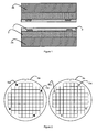
- the alignment detection means 1 are of the inductive type and formed at the faces facing the substrates 2 to be aligned, as illustrated very schematically in FIG. figure 1 .
- Each substrate 2 may comprise active components, for example transistors, metal interconnection levels 3 connecting the different active components to each other.
- the inductive type alignment detection means consist of microbubines 1, solenoid type or plane. Since microbobins 1 of the solenoid type are more complicated to produce and expensive, planar microbubines 1 are preferred.
- the microbubines 1 are advantageously formed in the metal interconnection levels and, preferably, in the last level of metal interconnection, the level farthest from the substrate 2.
- the microbubines 1 are produced after the manufacture of the metal interconnection levels. 3. They are preferably covered by a layer of dielectric material 4, for example of polymer material, mineral material, silicon nitride, or preferably silicon oxide, for molecular bonding.
- the layer 4 typically has a thickness of about 200 nm when flattened.
- microbubines 1 are preferably disposed at the periphery of the substrate 2. They are connected to electrical contact pads (not shown) via connecting lines. The contact pads make it possible to supply the microbubines 1 and / or to measure their overall inductance by means of an external processing circuit (not shown).
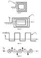
- the planar microbubines may, for example, be microbubines in a spiral, square shape ( figure 3 ) or lying down ( figure 4 ).
- Such square spiral microbubines 1 are commonly used in the field of microsystems and microelectronics.
- the realization of microbubines 1 in the form of a square spiral ( figure 3 ) is very well mastered. It is formed on the last level of metal interconnection. However, one of the connection lines (dotted on the figure 3 ) is performed on a lower interconnection level.
- the design must be integrated on two consecutive metal levels.
- the dimensions of this type of coil are dependent on the number of turns constituting it. This type of coil has fairly dispersive field lines, which provide a fairly large field of interaction with respect to the inner diameter of the microbobine 1. As a result, the accuracy obtained for alignment is limited and may be insufficient.
- a more accurate alignment can be obtained in a direction perpendicular to the elongation direction of an elongate spiral flat microbobine 1 ( figure 4 ), that is to say along an axis (Y) perpendicular to the main axis of the coil (X axis on the figure 4 ), of rectangular shape.
- the alignment is preferably carried out in two successive steps. A first alignment is made along a Y axis with microbobins having a main axis along X. Then, an alignment is made along X with microbobins perpendicular to the previous ones, that is to say, of the main axis along Y.
- the displacement and the alignment of a substrate 2 relative to the other are therefore carried out successively along axes perpendicular to the main axes of the microbobins 1 .
- microbobin 1 meander-shaped plane illustrated in the figure 5 .
- These microbubines are no longer in the form of a spiral but in the form of a coil.
- the field lines induced by this type of coil have the particularity of not bending back on themselves, but of interacting in a single direction, namely the main axis of the microbobine, that is to say according to the X direction on the figure 5 .
- This type of microbobine 1 provides better accuracy than that obtained with spiral coils.
- meander planar microbubines 1 are oriented in two directions, preferably perpendicular and the alignment is carried out in two successive steps.
- the displacement and the alignment of a substrate 2 with respect to the other are successively carried out along axes parallel to the main axes of the microbubines 1.
- meander planar coils The major advantage of meander planar coils is to present a much simpler embodiment from a technological point of view than solenoid coils, and even as square or elongated spiral planar coils. Indeed, in the case of meander coils, only one level of metal is necessary for the manufacture against two levels for the spirals square and much more for solenoids. When designing the circuits, all you have to do is reserve a slot for the microbobins and their realization is done at the same time as the last metal level of the circuit.
- the materials used in microbobins are conventional materials of microelectronics.
- the microbobins are made of copper and are isolated by a conventional dielectric, which eliminates problems of compatibility of materials and possible additional costs.
- each substrate comprises at least two planar microbubines 1 with main axes oriented in different directions. Even more advantageously, each substrate comprises two series of microbubines, each microbobine of a series having its main axis oriented in the same predefined direction, the directions of the two series being not parallel. Although the alignment is simpler when the main axes of the different series of microbubines 1 are perpendicular, it is possible to use non-perpendicular main axes.
- the alignment of the two substrates 2, with respect to each other, in a plane parallel to the substrates, is then performed. This alignment can be performed directly or advantageously in two stages. A first displacement and a first alignment are made with a first series of microbubines 1 oriented along a first main axis.
- a second series of microbobins 1 elongate along a second main axis is used to make a second displacement of the substrates together.
- the use of first and second dissociated displacements is particularly advantageous for finalizing the alignment of the substrates if the main axes are perpendicular. Indeed, the alignment along the second axis does not alter the alignment already made along the first main axis. In this way, by moving the substrates 2 relative to each other, in directions parallel to the main axes of the microbubines, it is possible to align the substrates with very high precision. In this way, morphological specificities of each of the coils can successively reduce the misalignment of the substrates 2 in two directions.
- the microbubines 1 are disposed on the surfaces of the substrates 2a and 2b so that two microbubines having substantially parallel main axes are facing each other during alignment.
- the microbubines 1 are disposed at the periphery of the substrates 2.
- at least two microbubines 1 x or 1 y having the same main direction are arranged symmetrically with respect to the center of the substrate.
- two sets of microbubines 1 x and 1 y are each constituted by two microbobins arranged symmetrically with respect to the center of each of the substrates 2a and 2b and at their periphery.
- microbubines are particularly advantageous for increasing the accuracy of the alignment.
- the microbubines 1 ax, respectively 1 ay are substantially opposite microbubines 1 bx, respectively 1 by. The alignment process can then be initiated.
- the microbobins 1 are conventionally made in the last level of metal interconnection in the form of copper lines having a typical section of the order of 100 ⁇ 100 nm 2 .
- the minimum spacing between two copper lines is of the order of 100 nm.
- the microbobins have a maximum size of a few microns, for example 5 ⁇ 5 ⁇ m 2 with an interspirar spacing of the order of 5 ⁇ m.
- the surface occupied by a microbobine 1 is typically less than 900 ⁇ m 2 .
- the number of turns of microbubines 1 is at least two and preferably equal to five.
- the microbubines being made in the last level of metal interconnection their thickness is predefined. However, if the thickness is incompatible with inductive performance required, a specific additional level can be achieved for the formation of microbobins.
- microbubines 1 of one of the substrates 2 are powered by an alternating current.
- the alignment of the substrates is then achieved by measuring the variation of inductance in the microbubines 1 of the other substrate, which are not powered. A variation of inductance around a zero value is measured since these microbubines are not powered.
- the microbubines 1 of the two substrates 2 are fed with two alternating currents, preferably of the same frequency, with a zero phase shift and of the same amplitude.
- the microbubines 1 are fed in such a way that the currents flowing through the two microbubines are directed in the same direction.
- the field lines induced by each of the coils are directed in the same direction.
- induced field lines are created around the wire forming the coil.
- the orientation of the field lines is a function of the direction of the current passing through the microbobine 1.
- the figure 6 illustrates the direction of the current, in the y direction, the induced field lines of a meander-shaped microbobine 1 according to the figure 4 cross-section along the X axis.
- the meanders of the microbobine cause the current I to have opposite directions in two adjacent portions perpendicular to the X axis.
- the induced field lines have opposite directions of rotation and are alternately distributed. It follows that the forces resulting from the interaction of these lines of fields, represented on the figure 6 by arrows parallel to the Z axis, are also opposed and alternately distributed.
- the microbubines 1 of one of the substrates are connected to inductance detection means, for example to a multimeter.
- the multimeter measures the inductance induced in the microbobine of the lower substrate 2a, by the corresponding microbobine of the upper substrate 2b.
- the value of the inductance variation induced in the lower microbobine by the upper microbobine is used directly to locate the position of the substrates together.
- the multimeter is conventionally connected to a processing circuit (not shown) which controls micro-positioning means.
- the alignment process is based on the fact that the inductive coupling is maximum when the two associated microbubines are perfectly opposite, that is to say are aligned on the same vertical axis.
- two identical microbobins 1, meander-shaped, are associated and the two microbubines are fed so that the currents flowing through the two microbubines are directed in the same direction.
- a single microbobine constituting the measuring microbobine is used to measure the ⁇ L inductance variation.
- the two microbubines being identical, their induced fields are also identical if the intensities crossing the two inductive circuits are equal. In this way, the resulting forces of each of the coils are identical in their intensity and their position with respect to the turns.
- the figures 6 and 7 illustrate different positions of two microbobins with respect to each other and the variation of the inductance ⁇ L of the measurement microbobine which results from the different interactions of the resulting forces.
- the microbobine 1a at the bottom of the figure, does not move, while the associated microbobine 1b is moved along the X axis and takes 5 positions different.
- the various illustrated positions will, along the X axis, a total misalignment (position A) to a full alignment (position E) of the two microbubines 1.
- the two microbubines 1a and 1b do not overlap at all. There is then no variation of the inductance L in the microbobine measurement 1a since the system is not disturbed. By reducing their misalignment, the inductance of the measuring microbobine varies. The induced field lines in the opposite branches (the rightmost branch of the microbobine 1b in displacement and the leftmost branch of the measuring microbobine 1 a) being in opposite directions, the variation of inductance is all first negative. When the two microbobins arrive in position B, in which the microbubines have a single opposite field line, in opposite directions, this field line is canceled and the overall inductance measured across the microbobine reaches a first minimum. By continuing the shift to the right of the microbobine 1b, the inductance increases because the interaction between the opposite induced field lines decreases and is gradually replaced by an interaction between field lines of the same direction.
- microbubines 1a and 1b have two facing field lines, which are oriented in the same direction.
- the coupling system strengthens rather than vanishes.
- the variation of inductance L reaches a first maximum, larger, in absolute value, than the maximum variation reached in the position B because two pairs of field lines are then in interaction instead of a single pair .
- in position D as in position B, the variation of inductance corresponds to the setting opposite opposite lines of fields. However, in position D, three field lines are involved and the inductance reaches a higher minimum, in absolute value, than the minimum reached. in the position B or the maximum reached in the position C.
- position E in which the two microbubines 1a and 1b are perfectly aligned along the X axis, all the field lines are facing and in the same direction which results in a maximum positive variation of the inductance.
- the alignment process here relies on the fact that all the induced fields resulting from microbubines 1a and 1b interact in a contructive and non-destructive manner when the position E is made.
- the amplitude of the variation of the inductance is also maximum, which corresponds to a minimum misalignment between the substrates.
- the amplitude of the variation of the inductance in the measuring microbobine is independent of the direction of the current flowing through the microbobins and depends only on the alignment between the microbubines.
- an inductance variation of 5% that is to say between 0.025 and 0.1 nH, can be detected for meander-shaped planar microbubines having an initial inductance of between 0.5. and 2nH.
- the inductive method can be achieved without direct contact between the substrates.
- the inductance variation is remotely detectable which means that the alignment can be performed by leaving a predetermined gap between the substrates during the alignment phase. In this way, the generation of defects at the bonding interface is zero since there is no contact between the two substrates.
- the distance separating the two substrates is typically in the range of a few microns to a few tens of microns, which makes it possible to relax the constraints on a control system of the separation distance.
- the typical distance is 10 ⁇ m for coils involving micrometric dimensions (typically between 1 and 5 ⁇ m) and currents of a few tens of milliamperes, for example 50mA.
Landscapes
- Engineering & Computer Science (AREA)
- Microelectronics & Electronic Packaging (AREA)
- Semiconductor Integrated Circuits (AREA)
- Measurement Of Resistance Or Impedance (AREA)
Abstract
Description
- L'invention est relative à un procédé d'alignement entre des premier et second substrats, ayant des faces en regard comportant des moyens de détection de l'alignement, procédé comportant, dans une phase d'alignement, le déplacement des substrats l'un par rapport à l'autre dans un plan parallèle aux substrats, la mesure d'une grandeur électrique associée aux moyens de détection de l'alignement et la détermination de l'alignement en fonction des variations de ladite grandeur.
- L'intégration tridimensionnelle représente un nouveau schéma d'intégration dans lequel plusieurs niveaux de composants actifs sont empilés les uns sur les autres et forment ainsi une puce multi-niveaux. D'un point de vue pratique, l'intégration tridimensionnelle consiste à reporter face-à-face deux substrats ayant des circuits intégrés complémentaires et à les coller pour ne former qu'une seule puce. Cependant, le principal problème est lié à l'alignement des deux circuits intégrés de manière à ce que les composants actifs de chacun des substrats puissent communiquer.
- Pour réaliser ce type d'intégration, les techniques d'alignement « substrat sur substrat », principalement utilisées dans le domaine des microsystèmes, par exemple pour les microsystèmes électromécaniques, offrent de nombreux avantages.
- Cependant, pour réaliser une intégration de type tridimensionnelle qui couple deux circuits intégrés ayant une forte densité en composants actifs, par exemple des transistors CMOS, il est nécessaire de posséder un système d'alignement de haute précision.
- Majoritairement, l'alignement de deux substrats est réalisé par des techniques optiques. De manière générale, des marques d'alignement sont formées sur chacun des substrats. Une tête de lecture optique détermine alors sur chacun des substrats les coordonnées des marques. L'alignement des substrats est alors réalisé en alignant les marques entre elles. De façon conventionnelle, un désalignement de l'ordre de 1µm est obtenu dans des conditions optimales de réalisation, ce qui limite l'intérêt de l'intégration tridimensionnelle, notamment en terme de densité d'intégration des interconnexions inter-niveaux.
- Une méthode capacitive a été développée, notamment dans le brevet
US 7193423 , pour remplacer la technique optique et atteindre de meilleures précisions d'alignement. Une structure de couplage capacitif est alors intégrée sur chacun des substrats, juste en dessous d'une couche d'oxyde servant au collage moléculaire. Les deux substrats sont ensuite mis en contact direct et un condensateur, constitué par les structures de couplages capacitifs des deux substrats séparés par l'oxyde de silicium, est alors formé. Le déplacement des substrats l'un par rapport à l'autre se traduit alors par une variation de la valeur de la capacité du condensateur qui peut alors être utilisée pour réaliser l'alignement. Une variation de capacité d'au moins 10-18F doit être obtenue pour un déplacement d'un nanomètre. - De nombreux inconvénients réduisent fortement l'intérêt de cette technique. En effet, la formation du condensateur implique que les deux couches d'oxyde de silicium soient en contact direct. En pratique, une interface de collage moléculaire est déjà formée, engendrant la création de liaisons faibles et le déplacement des substrats l'un par rapport à l'autre dans la phase d'alignement risque d'entraîner la formation de défauts dans l'interface de collage, ce qui diminue la fiabilité du collage et du circuit obtenu. De plus, l'alignement des substrats est lié à la mesure de la valeur de la capacité, elle-même dépendante de la distance qui sépare les deux électrodes du condensateur. Si l'épaisseur de la couche d'oxyde varie, la valeur de la capacité varie également. Ainsi, si la couche d'oxyde ne présente pas une épaisseur constante, il est difficile de réaliser un alignement fiable et utilisable industriellement.
- L'invention a pour objet un procédé d'alignement de deux substrats qui soit facile à mettre en oeuvre, qui présente une grande précision d'alignement et qui soit compatible avec les procédés de fabrication conventionnels.
- Le procédé selon l'invention est caractérisé en ce que les moyens de détection de l'alignement comportent des microbobines au niveau des faces en regard des premier et second substrats, et en ce que le procédé comporte au moins l'alimentation des microbobines du premier substrat et la mesure de l'inductance des microbobines du second substrat, ladite inductance constituant ladite grandeur électrique.
- D'autres avantages et caractéristiques ressortiront plus clairement de la description qui va suivre de modes particuliers de réalisation de l'invention donnés à titre d'exemples non limitatifs et représentés aux dessins annexés, dans lesquels :
- la
figure 1 représente, de façon schématique, en coupe, deux substrats en regard comportant chacun des moyens de mesure de l'alignement selon l'invention, - la
figure 2 illustre une disposition particulière des microbobines, - les
figures 3 à 5 représentent, de façon schématique, en vue de dessus, des exemples de réalisation de microbobines, - la
figure 6 représente, de façon schématique, le sens du courant et les lignes de champ résultant correspondant à une coupe selon l'axe X d'une microbobine selon lafigure 5 , - les
figures 7 et 8 représentent, de façon schématique, respectivement 5 positions de désalignement de deux microbobines en regard et la mesure de la variation d'inductance correspondante. - Selon l'invention, les moyens de détection de l'alignement 1 sont de type inductif et formés au niveau des faces en regard des substrats 2 à aligner, comme illustré très schématiquement à la
figure 1 . Chaque substrat 2 peut comporter des composants actifs, par exemple des transistors, des niveaux d'interconnexion métallique 3 connectant les différents composants actifs entre eux. Les moyens de détection de l'alignement de type inductif sont constitués par des microbobines 1, de type solénoïde ou plane. Les microbobines 1 de type solénoïde étant plus compliquées à réaliser et coûteuses, les microbobines 1 planes leurs sont préférées. - Les microbobines 1 sont avantageusement formées dans les niveaux d'interconnexion métallique et, de préférence, dans le dernier niveau d'interconnexion métallique, le niveau le plus éloigné du substrat 2. Les microbobines 1 sont réalisées après la fabrication des niveaux d'interconnexion métallique 3. Elles sont, de préférence, recouvertes par une couche en matériau diélectrique 4, par exemple en matériau polymère , en matériau minéral, en nitrure de silicium, ou avantageusement en oxyde de silicium, destinée au collage moléculaire. La couche 4 a typiquement une épaisseur de l'ordre de 200 nm une fois aplanie.
- Comme illustré à la
figure 2 , les microbobines 1 sont, de préférence, disposées à la périphérie du substrat 2. Elles sont connectées à des plots de contact électriques (non représentés) par l'intermédiaire de lignes de connexion. Les plots de contact permettent d'alimenter les microbobines 1 et/ou de mesurer leur inductance globale par l'intermédiaire d'un circuit de traitement extérieur (non représenté). - Comme illustré aux
figures 3 à 5 , différents types de microbobines 1 planes sont utilisables. Les microbobines planes peuvent, par exemple, être des microbobines en forme de spirale, carrée (figure 3 ) ou allongée (figure 4 ). De telles microbobines 1 planes en spirale carrée sont couramment utilisées dans le domaine des microsystèmes et de la microélectronique. La réalisation de microbobines 1 en forme de spirale carrée (figure 3 ) est très bien maîtrisée. Elle est formée sur le dernier niveau d'interconnexion métallique. Cependant, une des lignes de connexion (en pointillé sur lafigure 3 ) est réalisée sur un niveau d'interconnexion inférieur. La conception doit être intégrée sur deux niveaux de métal consécutifs. Les dimensions de ce type de bobine sont dépendantes du nombre de spires qui la constituent. Ce type de bobine a des lignes de champ assez dispersives, qui fournissent un champ d'interaction assez étendu par rapport au diamètre interne de la microbobine 1. En conséquence, la précision obtenue pour l'alignement est limitée et peut être insuffisante. - Un alignement plus précis peut être obtenu suivant une direction perpendiculaire à la direction d'élongation d'une microbobine 1 plane en spirale allongée (
figure 4 ), c'est-à-dire suivant un axe (Y) perpendiculaire à l'axe principal de la bobine (axe X sur lafigure 4 ), de forme rectangulaire. Pour obtenir un alignement satisfaisant des deux substrats 2, l'alignement est, de préférence, réalisé en deux étapes successives. Un premier alignement est réalisé selon un axe Y avec des microbobines ayant un axe principal selon X. Puis, un alignement est réalisé selon X avec des microbobines perpendiculaires aux précédentes, c'est-à-dire d'axe principal selon Y. Pour des microbobines planes en spirale allongée, le déplacement et l'alignement d'un substrat 2 par rapport à l'autre sont donc réalisés successivement selon des axes perpendiculaires aux axes principaux des microbobines 1. - Un autre type de microbobine 1 plane en forme de méandre, illustrée à la
figure 5 , est avantageusement utilisée. Ces microbobines ne sont plus en forme de spirale mais en forme de serpentin. Les lignes de champ induites par ce type de bobine ont la particularité de ne pas se reboucler sur elles-mêmes, mais d'interagir selon une seule direction, à savoir l'axe principal de la microbobine, c'est-à-dire selon la direction X sur lafigure 5 . Ce type de microbobine 1 permet d'obtenir une meilleure précision que celle obtenue avec des bobines en spirale. Comme précédemment, pour une précision optimale, des microbobines 1 planes en méandre sont orientées suivant deux directions, de préférence, perpendiculaires et l'alignement est réalisé en deux étapes successives. Cependant, pour des microbobines en forme de méandre, le déplacement et l'alignement d'un substrat 2 par rapport à l'autre sont réalisés successivement selon des axes parallèles aux axes principaux des microbobines 1. - L'avantage majeur des bobines planes à méandre est de présenter un mode de réalisation beaucoup plus simple d'un point de vue technologique que les bobines solénoïdales, et même que les bobines planes à spirale carrée ou allongée. En effet, dans le cas des bobines à méandre, seul un niveau de métal est nécessaire à la fabrication contre deux niveaux pour les spirales carrées et beaucoup plus pour les solénoïdes. Au moment de la conception des circuits, il suffit juste de réserver un emplacement pour les microbobines et leur réalisation se fait en même temps que le dernier niveau de métal du circuit. De plus, les matériaux utilisés dans les microbobines sont des matériaux classiques de la microélectronique. Les microbobines sont donc fabriquées en cuivre et sont isolées par un diélectrique conventionnel, ce qui élimine des problèmes de compatibilité des matériaux et des surcoûts éventuels.
- Avantageusement, chaque substrat comporte au moins deux microbobines 1 planes avec des axes principaux orientés suivant des directions différentes. Encore plus avantageusement, chaque substrat comporte deux séries de microbobines, chaque microbobine d'une série ayant son axe principal orienté suivant une même direction prédéfinie, les directions des deux séries n'étant pas parallèles. Bien que l'alignement soit plus simple lorsque les axes principaux des différentes séries de microbobines 1 sont perpendiculaires, il est envisageable d'utiliser des axes principaux non perpendiculaires. L'alignement des deux substrats 2, l'un par rapport à l'autre, dans un plan parallèle aux substrats, est alors réalisé. Cet alignement peut être effectué directement ou avantageusement en deux temps. Un premier déplacement et un premier alignement sont réalisés avec une première série de microbobines 1 orientées suivant un premier axe principal. Ensuite, une seconde série de microbobines 1 allongées suivant un second axe principal est utilisée pour réaliser un second déplacement des substrats entre eux. L'utilisation de premier et second déplacement dissociés est particulièrement avantageux pour finaliser l'alignement des substrats si les axes principaux sont perpendiculaires. En effet, l'alignement suivant le second axe ne modifie pas l'alignement déjà réalisé suivant le premier axe principal. De cette manière, en déplaçant les substrats 2, l'un par rapport à l'autre, suivant des directions parallèles aux axes principaux des microbobines, il est possible d'aligner les substrats avec une très grande précision. De cette manière, les spécificités morphologiques de chacune des bobines permettent de réduire successivement les désalignements des substrats 2 suivant deux directions.
- De manière générale, les microbobines 1 sont disposées sur les surfaces des substrats 2a et 2b de manière à ce que deux microbobines présentant des axes principaux sensiblement parallèles soient en regard lors de l'alignement. Dans un mode de réalisation préférentiel, illustré à la
figure 2 , les microbobines 1 sont disposées à la périphérie des substrats 2. Avantageusement, au moins deux microbobines 1 x ou 1 y présentant la même direction principale sont disposées symétriquement par rapport au centre du substrat. Sur lafigure 2 , deux séries de microbobines 1 x et 1 y sont chacune constituées par deux microbobines disposées symétriquement par rapport au centre de chacun des substrats 2a et 2b et à leur périphérie. Cette disposition des microbobines est particulièrement avantageuse pour augmenter la précision de l'alignement. De cette manière, lorsque les surfaces des substrats 2a et 2b, comportant les microbobines, sont mises en regard, les microbobines 1 ax, respectivement 1 ay, sont sensiblement en regard des microbobines 1 bx, respectivement 1 by. Le procédé d'alignement peut alors être initié. - Les microbobines 1 sont classiquement réalisées dans le dernier niveau d'interconnexion métallique sous la forme de lignes de cuivre ayant une section typique de l'ordre de 100x100nm2. L'espacement minimal entre deux lignes de cuivre est de l'ordre de 100nm. Typiquement, les microbobines ont des dimensions maximales de quelques microns, par exemple 5x5µm2 avec un espacement interspire de l'ordre de 5 µm. La surface occupée par une microbobine 1 est typiquement inférieure à 900µm2. De manière classique, le nombre de spires des microbobines 1 est au minimum de deux et préférentiellement égale à cinq. Typiquement, les microbobines étant réalisées dans le dernier niveau d'interconnexion métallique, leur épaisseur est prédéfinie. Cependant, si l'épaisseur est incompatible avec les performances inductives nécessaire, un niveau supplémentaire spécifique peut être réalisé pour la formation des microbobines.
- Dans un premier mode de réalisation du procédé d'alignement, seules les microbobines 1 de l'un des substrats 2 sont alimentées par un courant alternatif. L'alignement des substrats est alors réalisé en mesurant la variation d'inductance dans les microbobines 1 de l'autre substrat, qui ne sont pas alimentées. Une variation d'inductance autour d'une valeur nulle est mesurée puisque ces microbobines ne sont pas alimentées.
- Dans un second mode de réalisation, les microbobines 1 des deux substrats 2 sont alimentées par deux courants alternatifs, préférentiellement de même fréquence, avec un déphasage nul et de même amplitude. Les microbobines 1 sont alimentées de manière à ce que les courants qui traversent les deux microbobines soient dirigés dans le même sens. Ainsi, les lignes de champ induit par chacune des bobines sont dirigées dans le même sens. Une interaction optimale est alors obtenue quand les deux microbobines 1 sont parfaitement alignées, c'est-à-dire quand les deux substrats sont parfaitement alignés.
- Lors du passage d'un courant dans une microbobine 1, des lignes de champ induit sont créées autour du fil métallique formant la bobine. L'orientation des lignes de champ est fonction du sens du courant qui traverse la microbobine 1. La
figure 6 illustre le sens du courant, selon la direction y, les lignes de champ induit d'une microbobine 1 en forme de méandre selon lafigure 4 vue en coupe selon l'axe X. Les méandres de la microbobine font que le courant I a des sens opposés dans deux portions adjacentes perpendiculaires à l'axe X. En conséquence, dans une microbobine en forme de méandre, les lignes de champ induit ont des sens de rotation opposés et sont alternativement réparties. Il en résulte alors que les forces résultantes de l'interaction de ces lignes de champs, représentées sur lafigure 6 par des flèches parallèles à l'axe Z, sont également opposées et alternativement réparties. - Dans tous les cas, les microbobines 1 de l'un des substrats, par exemple le substrat inférieur 2a, sont connectées à des moyens de détection de l'inductance, par exemple à un multimètre. Le multimètre mesure l'inductance induite dans la microbobine du substrat inférieur 2a, par la microbobine correspondante du substrat supérieur 2b. La valeur de la variation de l'inductance induite dans la microbobine inférieure par la microbobine supérieure est utilisée directement pour localiser la position des substrats entre eux. Le multimètre est classiquement connecté à un circuit de traitement (non représenté) qui contrôle des moyens de micro-positionnement. Le processus d'alignement repose sur le fait que le couplage inductif est maximal lorsque les deux microbobines associées sont parfaitement en regard, c'est-à-dire sont alignées sur un même axe vertical.
- Dans le mode de réalisation particulier illustré aux
figures 6 et7 deux microbobines 1 identiques, en forme de méandre, sont associées et les deux microbobines sont alimentées de manière à ce que les courants qui traversent les deux microbobines soient dirigés dans le même sens. Une seule microbobine, constituant la microbobine de mesure, est utilisée pour mesurer la variation d'inductance ΔL. Les deux microbobines étant identiques, leurs champs induits le sont également si les intensités traversant les deux circuits inductifs sont égales. De cette manière, les forces résultantes de chacune des bobines sont identiques dans leur intensité et leur position par rapport aux spires. Lesfigures 6 et7 illustrent différentes positions de deux microbobines l'une par rapport à l'autre et la variation de l'inductance ΔL de la microbobine de mesure qui découle des différentes interactions des forces résultantes. Sur lafigure 7 , la microbobine de mesure 1a, à la partie inférieure de la figure, ne bouge pas, tandis que la microbobine 1b associée est déplacée selon l'axe X et prend 5 positions différentes. Les différentes positions illustrées vont, selon l'axe X, d'un désalignement total (position A) à un alignement (position E) complet des deux microbobines 1. - Dans la position A, les deux microbobines 1 a et 1 b ne se recouvrent pas du tout. Il n'y a alors aucune variation de l'inductance L dans la microbobine de mesure 1 a puisque le système n'est pas perturbé. En réduisant leur désalignement, l'inductance de la microbobine de mesure varie. Les lignes de champ induit dans les branches en regard (branche la plus à droite de la microbobine 1 b en déplacement et branche la plus à gauche de la microbobine de mesure 1 a) étant de sens opposés, la variation d'inductance est tout d'abord négative. Lorsque les deux microbobines arrivent dans la position B, dans laquelle les microbobines ont une seule ligne de champ en regard, de sens opposés, cette ligne de champ s'annule et l'inductance globale mesurée aux bornes de la microbobine de mesure atteint un premier minimum. En poursuivant le déplacement vers la droite de la microbobine 1 b, l'inductance augmente car l'interaction entre les lignes de champ induit de sens opposés diminue et est progressivement remplacée par une interaction entre des lignes de champ de même sens.
- Dans la position C, les microbobines 1 a et 1 b ont deux lignes de champ en regard, qui sont orientées dans le même sens. Le système de couplage se renforce au lieu de s'annuler. Dans la position C, la variation d'inductance L atteint un premier maximum, plus important, en valeur absolue, que la variation maximum atteinte dans la position B car deux couples de lignes de champ sont alors en interaction au lieu d'un seul couple.
- Dans la position D, comme dans la position B, la variation d'inductance correspond à la mise en regard de lignes de champs opposées. Cependant, dans la position D, trois lignes de champs sont mises en jeu et l'inductance atteint un minimum plus élevé, en valeur absolue, que le minimum atteint dans la position B ou que le maximum atteint dans la position C. Dans la position E, dans laquelle les deux microbobines 1 a et 1b sont parfaitement alignées selon l'axe X, toutes les lignes de champs sont en regard et dans le même sens, ce qui se traduit par une variation positive maximum de l'inductance. Le processus d'alignement repose ici sur le fait que tous les champs induits issus des microbobines 1a et 1b interagissent de manière contructive et non destructive lorsque la position E est réalisée.
- Il est ainsi possible de déterminer l'alignement maximal dès microbobines. Lorsque l'alignement des microbobines est maximal, l'amplitude de la variation de l'inductance est également maximale ce qui correspond à un désalignement minimal entre les substrats. L'amplitude de la variation de l'inductance dans la microbobine de mesure est indépendant du sens du courant qui traverse les microbobines et ne dépend que de l'alignement entre les microbobines.
- A titre d'exemple, on peut détecter une variation d'inductance de 5%, c'est-à-dire comprise entre 0,025 et 0,1 nH pour des microbobines planes en forme de méandre ayant une inductance initiale comprise entre 0,5 et 2nH.
- Contrairement à la méthode capacitive, l'alignement par la méthode inductive peut être réalisé sans contact direct entre les substrats. En effet, la variation d'inductance est détectable à distance ce qui signifie que l'alignement peut être effectué en laissant un intervalle prédéterminé entre les substrats pendant la phase d'alignement. De cette manière, la génération de défauts à l'interface de collage est nulle puisqu'il n'y a pas de contact entre les deux substrats. Par ailleurs, la distance séparant les deux substrats est typiquement comprise dans la gamme de quelques microns à quelques dizaines de microns, ce qui permet de relâcher les contraintes sur un système de contrôle de la distance de séparation. A titre d'exemple, la distance typique est de 10µm pour des bobines mettant en jeu des dimensions micrométriques (typiquement entre 1 et 5µm) et des courants de quelques dizaines de milliampères, par exemple 50mA.
Claims (12)
- Procédé d'alignement entre des premier et second substrats (2), les substrats (2) ayant des faces en regard comportant des moyens de détection de l'alignement (1), procédé comportant, dans une phase d'alignement, le déplacement des substrats (2) l'un par rapport à l'autre dans un plan parallèle aux substrats (2), la mesure d'une grandeur électrique associée aux moyens de détection de l'alignement et la détermination de l'alignement en fonction des variations de ladite grandeur, procédé caractérisé en ce que les moyens de détection de l'alignement comportent des microbobines (1) au niveau des faces en regard des premier et second substrats (2), et en ce que le procédé comporte au moins l'alimentation des microbobines (1) du premier substrat (2) et la mesure de l'inductance des microbobines (1) du second substrat (2), ladite inductance constituant ladite grandeur électrique.
- Procédé selon la revendication 1, caractérisé en ce que l'alignement des substrats (1) est maximal quand la variation de l'inductance mesurée est maximale.
- Procédé selon l'une des revendications 1 et 2, caractérisé en ce qu'il comporte l'alimentation des microbobines (1) des deux substrats (2).
- Procédé selon l'une quelconque des revendications 1 à 3, caractérisé en ce que les deux substrats (2) sont séparés par un intervalle prédéterminé pendant la phase d'alignement.
- Procédé selon l'une quelconque des revendications 1 à 4, caractérisé en ce que les microbobines (1) sont constituées par des microbobines planes.
- Procédé selon la revendication 5, caractérisé en ce que les microbobines (1) sont de type spirale carrée ou spirale allongée.
- Procédé selon la revendication 5, caractérisé en ce que les microbobines (1) sont de type microbobines en méandre.
- Procédé selon l'une quelconque des revendications 1 à 7, caractérisé en ce que des microbobines (1) comportant un axe principal, chaque substrat (2) comporte au moins deux séries de microbobines (1) ayant des axes principaux d'orientations différentes, chaque série comportant au moins deux microbobines disposées symétriquement par rapport au centre du substrat (2).
- Procédé selon la revendication 8, caractérisé en ce que les microbobines étant de type spirale allongée, le déplacement et l'alignement d'un substrat (2) par rapport à l'autre sont réalisés successivement selon des axes perpendiculaires aux axes principaux desdites microbobines (1).
- Procédé selon la revendication 8, caractérisé en ce que les microbobines étant en forme de méandre, le déplacement et l'alignement d'un substrat (2) par rapport à l'autre sont réalisés successivement selon des axes parallèles aux axes principaux desdites microbobines (1).
- Procédé selon l'une quelconques des revendications 8 à 10, caractérisé en ce que les axes principaux sont perpendiculaires.
- Procédé selon l'une quelconque des revendications 1 à 11, caractérisé en ce que les substrats (2) comportant des niveaux d'interconnexion métallique, les microbobines (1) sont réalisées dans le dernier niveau d'interconnexion métallique.
Applications Claiming Priority (1)
| Application Number | Priority Date | Filing Date | Title |
|---|---|---|---|
| FR0800957A FR2928030B1 (fr) | 2008-02-22 | 2008-02-22 | Procede d'alignement de deux substrats par des microbobines. |
Publications (2)
| Publication Number | Publication Date |
|---|---|
| EP2093797A1 true EP2093797A1 (fr) | 2009-08-26 |
| EP2093797B1 EP2093797B1 (fr) | 2017-05-31 |
Family
ID=39797433
Family Applications (1)
| Application Number | Title | Priority Date | Filing Date |
|---|---|---|---|
| EP09354005.2A Not-in-force EP2093797B1 (fr) | 2008-02-22 | 2009-02-10 | Procédé d'alignement de deux substrats par des microbobines |
Country Status (3)
| Country | Link |
|---|---|
| US (1) | US7902837B2 (fr) |
| EP (1) | EP2093797B1 (fr) |
| FR (1) | FR2928030B1 (fr) |
Families Citing this family (4)
| Publication number | Priority date | Publication date | Assignee | Title |
|---|---|---|---|---|
| US8569899B2 (en) * | 2009-12-30 | 2013-10-29 | Stmicroelectronics, Inc. | Device and method for alignment of vertically stacked wafers and die |
| CN102315197B (zh) * | 2010-07-09 | 2013-04-17 | 中国科学院微电子研究所 | 3d集成电路结构以及检测芯片结构是否对齐的方法 |
| US10634483B2 (en) | 2017-10-13 | 2020-04-28 | Invensense, Inc. | Sensor misalignment measuring device |
| CN115831936B (zh) * | 2021-09-16 | 2023-09-05 | 安徽奥飞声学科技有限公司 | 一种具有埋容的基板及其埋容测试方法 |
Citations (4)
| Publication number | Priority date | Publication date | Assignee | Title |
|---|---|---|---|---|
| EP0439136A2 (fr) * | 1990-01-23 | 1991-07-31 | Sumitomo Electric Industries, Ltd. | Méthode pour connecter électriquement et emballer un dispositif semi-conducteur |
| US20020110936A1 (en) * | 2000-12-22 | 2002-08-15 | Mitsubishi Denki Kabushiki Kaisha | Inductor recognition method, layout inspection method, computer readable recording medium in which a layout inspection program is recorded and process for a semiconductor device |
| US7193423B1 (en) | 2005-12-12 | 2007-03-20 | International Business Machines Corporation | Wafer-to-wafer alignments |
| DE102006001601A1 (de) * | 2006-01-11 | 2007-07-12 | Infineon Technologies Ag | Halbleiterwafer mit Rückseitenidentifizierung und Verfahren zur Herstellung desselben |
Family Cites Families (6)
| Publication number | Priority date | Publication date | Assignee | Title |
|---|---|---|---|---|
| US4371116A (en) * | 1978-04-04 | 1983-02-01 | Sage David M | Variable reactance alignment detector and control |
| DE10018982B4 (de) * | 2000-04-17 | 2016-08-11 | Byk-Gardner Gmbh | Vorrichtung und Verfahren zum Messen von Transmissions- und Reflexionseigenschaften von Gegenständen und Oberflächen |
| US6911664B2 (en) * | 2002-04-15 | 2005-06-28 | D-Wave Systems, Inc. | Extra-substrate control system |
| US6963061B2 (en) * | 2002-08-15 | 2005-11-08 | Motorola, Inc. | Orthogonal coupled transceiver |
| JP4478470B2 (ja) * | 2004-01-26 | 2010-06-09 | キヤノン株式会社 | 位置決めステージ装置 |
| JP5146983B2 (ja) * | 2005-11-16 | 2013-02-20 | シンジーテック株式会社 | 導電性ゴム部材 |
-
2008
- 2008-02-22 FR FR0800957A patent/FR2928030B1/fr not_active Expired - Fee Related
-
2009
- 2009-02-06 US US12/320,879 patent/US7902837B2/en not_active Expired - Fee Related
- 2009-02-10 EP EP09354005.2A patent/EP2093797B1/fr not_active Not-in-force
Patent Citations (4)
| Publication number | Priority date | Publication date | Assignee | Title |
|---|---|---|---|---|
| EP0439136A2 (fr) * | 1990-01-23 | 1991-07-31 | Sumitomo Electric Industries, Ltd. | Méthode pour connecter électriquement et emballer un dispositif semi-conducteur |
| US20020110936A1 (en) * | 2000-12-22 | 2002-08-15 | Mitsubishi Denki Kabushiki Kaisha | Inductor recognition method, layout inspection method, computer readable recording medium in which a layout inspection program is recorded and process for a semiconductor device |
| US7193423B1 (en) | 2005-12-12 | 2007-03-20 | International Business Machines Corporation | Wafer-to-wafer alignments |
| DE102006001601A1 (de) * | 2006-01-11 | 2007-07-12 | Infineon Technologies Ag | Halbleiterwafer mit Rückseitenidentifizierung und Verfahren zur Herstellung desselben |
Also Published As
| Publication number | Publication date |
|---|---|
| US7902837B2 (en) | 2011-03-08 |
| FR2928030B1 (fr) | 2010-03-26 |
| US20090215207A1 (en) | 2009-08-27 |
| FR2928030A1 (fr) | 2009-08-28 |
| EP2093797B1 (fr) | 2017-05-31 |
Similar Documents
| Publication | Publication Date | Title |
|---|---|---|
| EP2816597A2 (fr) | Procédé de réalisation d'un dispositif microélectronique mécaniquement autonome | |
| EP2054929B1 (fr) | Procede de fabrication collective de modules electroniques 3d | |
| US9691970B2 (en) | Magnetoresistive devices and methods for manufacturing magnetoresistive devices | |
| EP2093797B1 (fr) | Procédé d'alignement de deux substrats par des microbobines | |
| EP1966825B1 (fr) | Procede de fabrication collective de modules electroniques 3d | |
| WO1996015461A1 (fr) | Procede de realisation de transducteurs magnetoresistifs | |
| WO2021099713A1 (fr) | Procede de fabrication d'une puce fonctionnelle adaptee pour etre assemblee a des elements filaires | |
| EP2274632B1 (fr) | Structure et procédé de fabrication d'un capteur de gradient de champ magnétique en technologie intégrée | |
| CN102147452A (zh) | 磁场传感器 | |
| EP2610906A1 (fr) | Procédé de fabrication collective de modules électroniques 3D ne comportant que des circuits imprimés validés | |
| FR3035220A1 (fr) | " dispositif electronique de mesure d'au moins une caracteristique electrique d'un objet " | |
| EP1852707B1 (fr) | Micromagnetometre de type fluxgate a bobinage d'excitation ameliore | |
| EP2546188A1 (fr) | Procédé de réalisation d'une structure a membrane suspendue et à électrode enterrée | |
| EP2823273A1 (fr) | Procede de fabrication d'un capteur de pression et capteur correspondant | |
| US20240347223A1 (en) | Micro-Fabricated Device for Controlling Trapped Ions and Method of Manufacturing the Same by Micro-Fabrication | |
| EP1788514B1 (fr) | Micromodule électronique et procédé de fabrication | |
| FR2959350A1 (fr) | Procede de fabrication d’un dispositif microelectronique et dispositif microelectronique ainsi fabrique | |
| EP3182450A1 (fr) | Dispositif d'inductance et son procédé de fabrication | |
| TW201321759A (zh) | 包含複數個高長寬比的電氣管路之分隔件和系統及製造方法和用途 | |
| FR3028328A1 (fr) | Procede de controle de positionnement relatif | |
| FR3057404A1 (fr) | Procede de generation d'une pluralite de courants presentant chacun une frequence | |
| WO2017140661A1 (fr) | Procede d'interconnexion chip on chip miniaturisee d'un module electronique 3d | |
| EP2960657A1 (fr) | Procede de caracterisation d'un dispositif de connexion electrique destine a etre contacte a un dispositif electronique | |
| FR2917231A1 (fr) | Realisation de condensateurs dotes de moyens pour diminuer les contraintes du materiau metallique de son armature inferieure | |
| FR3026560A1 (fr) | Structure d'encapsulation pourvue d'un capot et d'un substrat, pour connecter au moins un nano-objet sur une face du substrat et en reprendre le contact au travers du capot, et procede de fabrication de la structure |
Legal Events
| Date | Code | Title | Description |
|---|---|---|---|
| PUAI | Public reference made under article 153(3) epc to a published international application that has entered the european phase |
Free format text: ORIGINAL CODE: 0009012 |
|
| AK | Designated contracting states |
Kind code of ref document: A1 Designated state(s): AT BE BG CH CY CZ DE DK EE ES FI FR GB GR HR HU IE IS IT LI LT LU LV MC MK MT NL NO PL PT RO SE SI SK TR |
|
| AX | Request for extension of the european patent |
Extension state: AL BA RS |
|
| 17P | Request for examination filed |
Effective date: 20100201 |
|
| AKX | Designation fees paid |
Designated state(s): AT BE BG CH CY CZ DE DK EE ES FI FR GB GR HR HU IE IS IT LI LT LU LV MC MK MT NL NO PL PT RO SE SI SK TR |
|
| RAP1 | Party data changed (applicant data changed or rights of an application transferred) |
Owner name: COMMISSARIAT A L'ENERGIE ATOMIQUE ET AUX ENERGIES |
|
| REG | Reference to a national code |
Ref country code: DE Ref legal event code: R079 Ref document number: 602009046329 Country of ref document: DE Free format text: PREVIOUS MAIN CLASS: H01L0023544000 Ipc: B81C0003000000 |
|
| GRAP | Despatch of communication of intention to grant a patent |
Free format text: ORIGINAL CODE: EPIDOSNIGR1 |
|
| STAA | Information on the status of an ep patent application or granted ep patent |
Free format text: STATUS: GRANT OF PATENT IS INTENDED |
|
| INTG | Intention to grant announced |
Effective date: 20170109 |
|
| RIC1 | Information provided on ipc code assigned before grant |
Ipc: H01L 25/065 20060101ALI20161220BHEP Ipc: H01L 23/64 20060101ALI20161220BHEP Ipc: H01L 25/00 20060101ALI20161220BHEP Ipc: B81C 3/00 20060101AFI20161220BHEP |
|
| GRAS | Grant fee paid |
Free format text: ORIGINAL CODE: EPIDOSNIGR3 |
|
| GRAA | (expected) grant |
Free format text: ORIGINAL CODE: 0009210 |
|
| STAA | Information on the status of an ep patent application or granted ep patent |
Free format text: STATUS: THE PATENT HAS BEEN GRANTED |
|
| AK | Designated contracting states |
Kind code of ref document: B1 Designated state(s): AT BE BG CH CY CZ DE DK EE ES FI FR GB GR HR HU IE IS IT LI LT LU LV MC MK MT NL NO PL PT RO SE SI SK TR |
|
| REG | Reference to a national code |
Ref country code: CH Ref legal event code: EP Ref country code: GB Ref legal event code: FG4D Free format text: NOT ENGLISH |
|
| REG | Reference to a national code |
Ref country code: AT Ref legal event code: REF Ref document number: 897271 Country of ref document: AT Kind code of ref document: T Effective date: 20170615 |
|
| REG | Reference to a national code |
Ref country code: IE Ref legal event code: FG4D Free format text: LANGUAGE OF EP DOCUMENT: FRENCH |
|
| REG | Reference to a national code |
Ref country code: DE Ref legal event code: R096 Ref document number: 602009046329 Country of ref document: DE |
|
| REG | Reference to a national code |
Ref country code: NL Ref legal event code: MP Effective date: 20170531 |
|
| REG | Reference to a national code |
Ref country code: LT Ref legal event code: MG4D |
|
| REG | Reference to a national code |
Ref country code: AT Ref legal event code: MK05 Ref document number: 897271 Country of ref document: AT Kind code of ref document: T Effective date: 20170531 |
|
| PG25 | Lapsed in a contracting state [announced via postgrant information from national office to epo] |
Ref country code: FI Free format text: LAPSE BECAUSE OF FAILURE TO SUBMIT A TRANSLATION OF THE DESCRIPTION OR TO PAY THE FEE WITHIN THE PRESCRIBED TIME-LIMIT Effective date: 20170531 Ref country code: GR Free format text: LAPSE BECAUSE OF FAILURE TO SUBMIT A TRANSLATION OF THE DESCRIPTION OR TO PAY THE FEE WITHIN THE PRESCRIBED TIME-LIMIT Effective date: 20170901 Ref country code: LT Free format text: LAPSE BECAUSE OF FAILURE TO SUBMIT A TRANSLATION OF THE DESCRIPTION OR TO PAY THE FEE WITHIN THE PRESCRIBED TIME-LIMIT Effective date: 20170531 Ref country code: ES Free format text: LAPSE BECAUSE OF FAILURE TO SUBMIT A TRANSLATION OF THE DESCRIPTION OR TO PAY THE FEE WITHIN THE PRESCRIBED TIME-LIMIT Effective date: 20170531 Ref country code: HR Free format text: LAPSE BECAUSE OF FAILURE TO SUBMIT A TRANSLATION OF THE DESCRIPTION OR TO PAY THE FEE WITHIN THE PRESCRIBED TIME-LIMIT Effective date: 20170531 Ref country code: NO Free format text: LAPSE BECAUSE OF FAILURE TO SUBMIT A TRANSLATION OF THE DESCRIPTION OR TO PAY THE FEE WITHIN THE PRESCRIBED TIME-LIMIT Effective date: 20170831 Ref country code: AT Free format text: LAPSE BECAUSE OF FAILURE TO SUBMIT A TRANSLATION OF THE DESCRIPTION OR TO PAY THE FEE WITHIN THE PRESCRIBED TIME-LIMIT Effective date: 20170531 |
|
| PG25 | Lapsed in a contracting state [announced via postgrant information from national office to epo] |
Ref country code: IS Free format text: LAPSE BECAUSE OF FAILURE TO SUBMIT A TRANSLATION OF THE DESCRIPTION OR TO PAY THE FEE WITHIN THE PRESCRIBED TIME-LIMIT Effective date: 20170930 Ref country code: LV Free format text: LAPSE BECAUSE OF FAILURE TO SUBMIT A TRANSLATION OF THE DESCRIPTION OR TO PAY THE FEE WITHIN THE PRESCRIBED TIME-LIMIT Effective date: 20170531 Ref country code: SE Free format text: LAPSE BECAUSE OF FAILURE TO SUBMIT A TRANSLATION OF THE DESCRIPTION OR TO PAY THE FEE WITHIN THE PRESCRIBED TIME-LIMIT Effective date: 20170531 Ref country code: NL Free format text: LAPSE BECAUSE OF FAILURE TO SUBMIT A TRANSLATION OF THE DESCRIPTION OR TO PAY THE FEE WITHIN THE PRESCRIBED TIME-LIMIT Effective date: 20170531 Ref country code: BG Free format text: LAPSE BECAUSE OF FAILURE TO SUBMIT A TRANSLATION OF THE DESCRIPTION OR TO PAY THE FEE WITHIN THE PRESCRIBED TIME-LIMIT Effective date: 20170831 |
|
| PG25 | Lapsed in a contracting state [announced via postgrant information from national office to epo] |
Ref country code: CZ Free format text: LAPSE BECAUSE OF FAILURE TO SUBMIT A TRANSLATION OF THE DESCRIPTION OR TO PAY THE FEE WITHIN THE PRESCRIBED TIME-LIMIT Effective date: 20170531 Ref country code: RO Free format text: LAPSE BECAUSE OF FAILURE TO SUBMIT A TRANSLATION OF THE DESCRIPTION OR TO PAY THE FEE WITHIN THE PRESCRIBED TIME-LIMIT Effective date: 20170531 Ref country code: DK Free format text: LAPSE BECAUSE OF FAILURE TO SUBMIT A TRANSLATION OF THE DESCRIPTION OR TO PAY THE FEE WITHIN THE PRESCRIBED TIME-LIMIT Effective date: 20170531 Ref country code: EE Free format text: LAPSE BECAUSE OF FAILURE TO SUBMIT A TRANSLATION OF THE DESCRIPTION OR TO PAY THE FEE WITHIN THE PRESCRIBED TIME-LIMIT Effective date: 20170531 Ref country code: SK Free format text: LAPSE BECAUSE OF FAILURE TO SUBMIT A TRANSLATION OF THE DESCRIPTION OR TO PAY THE FEE WITHIN THE PRESCRIBED TIME-LIMIT Effective date: 20170531 |
|
| REG | Reference to a national code |
Ref country code: FR Ref legal event code: PLFP Year of fee payment: 10 |
|
| PG25 | Lapsed in a contracting state [announced via postgrant information from national office to epo] |
Ref country code: PL Free format text: LAPSE BECAUSE OF FAILURE TO SUBMIT A TRANSLATION OF THE DESCRIPTION OR TO PAY THE FEE WITHIN THE PRESCRIBED TIME-LIMIT Effective date: 20170531 Ref country code: IT Free format text: LAPSE BECAUSE OF FAILURE TO SUBMIT A TRANSLATION OF THE DESCRIPTION OR TO PAY THE FEE WITHIN THE PRESCRIBED TIME-LIMIT Effective date: 20170531 |
|
| REG | Reference to a national code |
Ref country code: DE Ref legal event code: R097 Ref document number: 602009046329 Country of ref document: DE |
|
| PLBE | No opposition filed within time limit |
Free format text: ORIGINAL CODE: 0009261 |
|
| STAA | Information on the status of an ep patent application or granted ep patent |
Free format text: STATUS: NO OPPOSITION FILED WITHIN TIME LIMIT |
|
| 26N | No opposition filed |
Effective date: 20180301 |
|
| PG25 | Lapsed in a contracting state [announced via postgrant information from national office to epo] |
Ref country code: SI Free format text: LAPSE BECAUSE OF FAILURE TO SUBMIT A TRANSLATION OF THE DESCRIPTION OR TO PAY THE FEE WITHIN THE PRESCRIBED TIME-LIMIT Effective date: 20170531 |
|
| REG | Reference to a national code |
Ref country code: CH Ref legal event code: PL |
|
| PG25 | Lapsed in a contracting state [announced via postgrant information from national office to epo] |
Ref country code: MC Free format text: LAPSE BECAUSE OF FAILURE TO SUBMIT A TRANSLATION OF THE DESCRIPTION OR TO PAY THE FEE WITHIN THE PRESCRIBED TIME-LIMIT Effective date: 20170531 Ref country code: MT Free format text: LAPSE BECAUSE OF FAILURE TO SUBMIT A TRANSLATION OF THE DESCRIPTION OR TO PAY THE FEE WITHIN THE PRESCRIBED TIME-LIMIT Effective date: 20170531 |
|
| GBPC | Gb: european patent ceased through non-payment of renewal fee |
Effective date: 20180210 |
|
| REG | Reference to a national code |
Ref country code: IE Ref legal event code: MM4A |
|
| REG | Reference to a national code |
Ref country code: BE Ref legal event code: MM Effective date: 20180228 |
|
| PG25 | Lapsed in a contracting state [announced via postgrant information from national office to epo] |
Ref country code: LU Free format text: LAPSE BECAUSE OF NON-PAYMENT OF DUE FEES Effective date: 20180210 Ref country code: CH Free format text: LAPSE BECAUSE OF NON-PAYMENT OF DUE FEES Effective date: 20180228 Ref country code: LI Free format text: LAPSE BECAUSE OF NON-PAYMENT OF DUE FEES Effective date: 20180228 |
|
| PG25 | Lapsed in a contracting state [announced via postgrant information from national office to epo] |
Ref country code: IE Free format text: LAPSE BECAUSE OF NON-PAYMENT OF DUE FEES Effective date: 20180210 |
|
| PG25 | Lapsed in a contracting state [announced via postgrant information from national office to epo] |
Ref country code: BE Free format text: LAPSE BECAUSE OF NON-PAYMENT OF DUE FEES Effective date: 20180228 Ref country code: GB Free format text: LAPSE BECAUSE OF NON-PAYMENT OF DUE FEES Effective date: 20180210 |
|
| PG25 | Lapsed in a contracting state [announced via postgrant information from national office to epo] |
Ref country code: TR Free format text: LAPSE BECAUSE OF FAILURE TO SUBMIT A TRANSLATION OF THE DESCRIPTION OR TO PAY THE FEE WITHIN THE PRESCRIBED TIME-LIMIT Effective date: 20170531 |
|
| PG25 | Lapsed in a contracting state [announced via postgrant information from national office to epo] |
Ref country code: PT Free format text: LAPSE BECAUSE OF FAILURE TO SUBMIT A TRANSLATION OF THE DESCRIPTION OR TO PAY THE FEE WITHIN THE PRESCRIBED TIME-LIMIT Effective date: 20170531 Ref country code: HU Free format text: LAPSE BECAUSE OF FAILURE TO SUBMIT A TRANSLATION OF THE DESCRIPTION OR TO PAY THE FEE WITHIN THE PRESCRIBED TIME-LIMIT; INVALID AB INITIO Effective date: 20090210 |
|
| PG25 | Lapsed in a contracting state [announced via postgrant information from national office to epo] |
Ref country code: CY Free format text: LAPSE BECAUSE OF FAILURE TO SUBMIT A TRANSLATION OF THE DESCRIPTION OR TO PAY THE FEE WITHIN THE PRESCRIBED TIME-LIMIT Effective date: 20170531 Ref country code: MK Free format text: LAPSE BECAUSE OF NON-PAYMENT OF DUE FEES Effective date: 20170531 |
|
| PGFP | Annual fee paid to national office [announced via postgrant information from national office to epo] |
Ref country code: FR Payment date: 20210226 Year of fee payment: 13 |
|
| PGFP | Annual fee paid to national office [announced via postgrant information from national office to epo] |
Ref country code: DE Payment date: 20210209 Year of fee payment: 13 |
|
| REG | Reference to a national code |
Ref country code: DE Ref legal event code: R119 Ref document number: 602009046329 Country of ref document: DE |
|
| PG25 | Lapsed in a contracting state [announced via postgrant information from national office to epo] |
Ref country code: FR Free format text: LAPSE BECAUSE OF NON-PAYMENT OF DUE FEES Effective date: 20220228 |
|
| PG25 | Lapsed in a contracting state [announced via postgrant information from national office to epo] |
Ref country code: DE Free format text: LAPSE BECAUSE OF NON-PAYMENT OF DUE FEES Effective date: 20220901 |