EP2091312B2 - Stackable electronics housing with multi-pin connector or female connector - Google Patents
Stackable electronics housing with multi-pin connector or female connector Download PDFInfo
- Publication number
- EP2091312B2 EP2091312B2 EP09150924.0A EP09150924A EP2091312B2 EP 2091312 B2 EP2091312 B2 EP 2091312B2 EP 09150924 A EP09150924 A EP 09150924A EP 2091312 B2 EP2091312 B2 EP 2091312B2
- Authority
- EP
- European Patent Office
- Prior art keywords
- unlocking
- pin
- housing
- pin strip
- strip
- Prior art date
- Legal status (The legal status is an assumption and is not a legal conclusion. Google has not performed a legal analysis and makes no representation as to the accuracy of the status listed.)
- Active
Links
- 238000009434 installation Methods 0.000 description 3
- 230000002035 prolonged effect Effects 0.000 description 1
- 238000000926 separation method Methods 0.000 description 1
Images


Classifications
-
- H—ELECTRICITY
- H01—ELECTRIC ELEMENTS
- H01R—ELECTRICALLY-CONDUCTIVE CONNECTIONS; STRUCTURAL ASSOCIATIONS OF A PLURALITY OF MUTUALLY-INSULATED ELECTRICAL CONNECTING ELEMENTS; COUPLING DEVICES; CURRENT COLLECTORS
- H01R13/00—Details of coupling devices of the kinds covered by groups H01R12/70 or H01R24/00 - H01R33/00
- H01R13/62—Means for facilitating engagement or disengagement of coupling parts or for holding them in engagement
- H01R13/629—Additional means for facilitating engagement or disengagement of coupling parts, e.g. aligning or guiding means, levers, gas pressure electrical locking indicators, manufacturing tolerances
- H01R13/62933—Comprising exclusively pivoting lever
-
- H—ELECTRICITY
- H01—ELECTRIC ELEMENTS
- H01R—ELECTRICALLY-CONDUCTIVE CONNECTIONS; STRUCTURAL ASSOCIATIONS OF A PLURALITY OF MUTUALLY-INSULATED ELECTRICAL CONNECTING ELEMENTS; COUPLING DEVICES; CURRENT COLLECTORS
- H01R9/00—Structural associations of a plurality of mutually-insulated electrical connecting elements, e.g. terminal strips or terminal blocks; Terminals or binding posts mounted upon a base or in a case; Bases therefor
- H01R9/22—Bases, e.g. strip, block, panel
- H01R9/24—Terminal blocks
- H01R9/26—Clip-on terminal blocks for side-by-side rail- or strip-mounting
- H01R9/2625—Clip-on terminal blocks for side-by-side rail- or strip-mounting with built-in electrical component
-
- H—ELECTRICITY
- H05—ELECTRIC TECHNIQUES NOT OTHERWISE PROVIDED FOR
- H05K—PRINTED CIRCUITS; CASINGS OR CONSTRUCTIONAL DETAILS OF ELECTRIC APPARATUS; MANUFACTURE OF ASSEMBLAGES OF ELECTRICAL COMPONENTS
- H05K7/00—Constructional details common to different types of electric apparatus
- H05K7/14—Mounting supporting structure in casing or on frame or rack
- H05K7/1462—Mounting supporting structure in casing or on frame or rack for programmable logic controllers [PLC] for automation or industrial process control
- H05K7/1468—Mechanical features of input/output (I/O) modules
- H05K7/1469—Terminal blocks for connecting sensors
Definitions
- the invention relates to a stackable housing arrangement according to claim 1 with a housing, in particular electronics housing.
- Such a housing is of the generic type EP 1 083 637 A known.
- the DE 10 2004 002 737 A1 relates to a release mechanism for a latched plug or socket part of an electrical connector, in particular a plug module from the base terminal of a field bus for the parallel wiring of actuators and sensors.
- at least one pivotally mounted lever is arranged transversely to the direction of pull of the plug module on at least one longitudinal recess of the plug module and is designed as an eccentric at one end.
- the electronics housing is designed as a module that can be snapped onto a mounting rail, the installation conditions are generally quite narrow.
- the object of the invention is to solve this problem with simple constructive means.
- the unlocking device supports the detachment of the plug connection between the plug and the socket strip in a simple manner. Unlocking is thus to be understood as at least supporting the separation of the two elements of the pin strip and socket strip from one another. It advantageously does not enlarge the overall width of the actual housing, in particular the electronics housing, in the direction of attachment, so that it is excellently suited for use on terminal block-type housings.
- Only one or more pin headers and / or socket headers can be arranged on the electronics housing.
- One of the unlocking devices is preferably assigned to each such terminal strip.
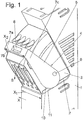
- Figure 1 shows a portion of an electronics housing 1, which preferably has a terminal-like structure in a manner not shown and is designed for snapping onto a mounting rail, not shown here.
- the direction of installation on the mounting rail is in Figure 1 indicated by the direction of arrow X.
- the housing has an X1 width.
- the installation space in the direction X is relatively short, for example the electronics housing 1 can have a width X1 of only a few millimeters.
- At least one pin strip 2 is arranged or formed on the electronics housing 1, which can be firmly connected to the electronics housing 1 or even in one piece with the housing, which surrounds the contact pins (not shown here).
- a socket strip 3 is plugged onto the pin strip 2, which can be placed essentially vertically or slightly obliquely to the vertical (relative to the mounting rail) from above onto the pin strip 2 and can preferably be latched to it and detachable from it in the opposite direction.
- an unlocking device 4 is arranged on the socket strip 3, which is designed here as a pivotable unlocking bracket 5, which is articulated on opposite sides of the socket strip 2 with the socket strip 2 on axes of rotation 6.
- the unlocking bracket 5 essentially has a U-shape with a base leg 7a and two side legs 7b, 7c.
- the unlocking bracket 5 engages around the socket strip 3 from above, the base leg 7a being arranged essentially above (relative to the support rail) of the socket strip 3 and here being pivotable in the direction of the arrow S in the direction of the support rail.
- the base leg 7a preferably has an actuating contour 8 for attaching a tool, which here is designed as a slot for attaching a screwdriver 9. A manual actuation on an attachment of the bracket or the like would also be conceivable (not shown here).
- the two longitudinal legs 7b, 7c aligned parallel to one another are in turn preferably parallel to the main outer surfaces 8a, 8b of the electronics housing, which are located in the row direction (or against the row direction) X.
- the socket strip with the unlocking device and the unlocking bracket 5 advantageously has a width X2 in the direction of attachment which is at least not greater or even smaller than the grid width X1 of the electronics housing in the direction of attachment. In this way, the unlocking device does not increase the overall width of the electronics housing in the direction X.
- unlocking bracket 5 is aligned with the main outer walls of the electronics housing 1 in the direction of the row.
- this unlocking contour 10 which has an eccentrically extending contour relative to the pivot axes 6, this unlocking contour 10 being located on a support surface 11 of the electronics housing (or alternatively the pin strip, not shown here ) supports. It is particularly preferred if the unlocking contour 10 is supported on the electronics housing 1.
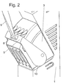
- the unlocking bracket 5 is now pivoted downward about the pivot axes 6 using a screwdriver 12, so that the unlocking contour 10, the distance from the pivot axis 6 of which increases with the pivoting of the unlocking bracket into the release position (here downward), the socket strip 3 from the pin header 2, since the unlocking contour 10 is supported on the support surface 11 in the manner of an abutment.
- a slot 12 on the unlocking bracket 5 which slot has an arc shape and is designed to interact with a pin 13 on the pin header 1 or on the electronics housing 1.
- the slot is open at one end and extends essentially perpendicular to the plug-in direction in which the socket strip is attached and detached.
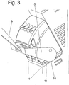
- the unlocking bracket 5 is moved into its lower position in this illustration - the unlocking position - so that the socket strip 3 can be plugged onto the pin strip 2 and locked there.
Description
Die Erfindung betrifft eine anreihbare Gehäuseanordnung nach Anspruch 1 mit einem Gehäuse, insbesondere Elektronikgehäuse.The invention relates to a stackable housing arrangement according to
Ein solches Gehäuse ist aus der gattungsgemäßen
Es ist bekannt, an Elektronikgehäusen eine oder mehrere Stiftleisten und/oder Buchsenleisten anzuordnen, die mit einer korrespondierenden Buchsenleiste bzw. Stiftleiste zusammensteckbar sind.It is known to arrange one or more pin headers and / or socket headers on electronics housings, which can be plugged together with a corresponding female headers or pin headers.
Insbesondere bei einer Auslegung der Elektronikgehäuse als auf eine Tragschiene rastbarer Baustein sind die Einbauverhältnisse in der Regel recht beengt.In particular, when the electronics housing is designed as a module that can be snapped onto a mounting rail, the installation conditions are generally quite narrow.
In diesem Fall ist es wie beim Stand der Technik oftmals relativ mühsam, einmal miteinander verbundene Stift- und Buchsenleisten wieder voneinander zu lösen.In this case, as in the prior art, it is often relatively cumbersome to detach pin and socket strips that have been connected to one another once again.
Die Erfindung hat die Aufgabe, dieses Problem mit einfachen konstruktiven Mitteln zu beheben.The object of the invention is to solve this problem with simple constructive means.
Die Erfindung erreicht dieses Ziel durch den Gegenstand des Anspruchs 1.The invention achieves this aim by the subject matter of
Die Entriegelungsvorrichtung unterstützt in einfacher Weise das Lösen der Steckverbindung zwischen der Steck- und der Buchsenleiste. Unter einem Entriegeln ist damit zumindest ein Unterstützen des Trennens der beiden Elemente Stiftleiste und Buchsenleiste voneinander zu verstehen. Sie vergrößert fern in vorteilhafter Weise nicht die Baubreite des eigentlichen Gehäuses, insbesondere des Elektronikgehäuses in Anreihrichtung, so dass sie sich hervorragend zum Einsatz an reihenklemmenartigen Gehäusen eignet.The unlocking device supports the detachment of the plug connection between the plug and the socket strip in a simple manner. Unlocking is thus to be understood as at least supporting the separation of the two elements of the pin strip and socket strip from one another. It advantageously does not enlarge the overall width of the actual housing, in particular the electronics housing, in the direction of attachment, so that it is excellently suited for use on terminal block-type housings.
Es können an dem Elektronikgehäuse nur eine oder auch mehrere Stiftleisten und/oder Buchsenleisten angeordnet sein. Dabei wird vorzugsweise jeder derartigen Anschlussleiste eine der Entriegelungsvorrichtungen zugeordnet.Only one or more pin headers and / or socket headers can be arranged on the electronics housing. One of the unlocking devices is preferably assigned to each such terminal strip.
Mit der vorteilhaften Ausgestaltung des Anspruchs 3 ist es darüber hinaus möglich im montierten Zustand, z.B. in rauer Umgebung an einer Maschine o.dgl., auch nach längerem Einsatz einen sicheren Zusammenhalt der Stift- und Buchsenleiste bzw. elektrischen Kontakte sicherzustellen.With the advantageous embodiment of
Vorteilhafte Ausgestaltungen der Erfindung sind den Unteransprüchen zu entnehmen.Advantageous embodiments of the invention can be found in the subclaims.
Nachfolgend wird die Erfindung unter Bezug auf die Zeichnungen anhand von Ausführungsbeispielen näher beschrieben. Es zeigt:
Figur 1- einen Teilbereich eines Elektronikgehäuses mit einer Stiftleiste, auf das eine Buchsenleiste mit einer Entriegelungsvorrichtung aufgesteckt ist;
Figur 2 bis 4- in aufeinanderfolgenden Schritten das Lösen bzw. Entriegeln der Buchsenleiste von dem Elektronikgehäuse mit der Stiftleiste nach
Figur 1 Figur 5- eine Teilbereich eines weiteren Elektronikgehäuses mit einer Stiftleiste, auf das eine Buchsenleiste mit einer kombinierten Ent- und Verriegelungsvorrichtung aufgesteckt ist; und
- Figur 6 bis 8
- in aufeinanderfolgenden Schritten das Lösen bzw. Entriegeln der Buchsenleiste von dem Elektronikgehäuse mit der Stiftleiste nach
Figur 5
- Figure 1
- a portion of an electronics housing with a pin header, on which a female connector with an unlocking device is attached;
- Figure 2 to 4
- in successive steps, releasing or unlocking the socket strip from the electronics housing using the pin strip
Figure 1 ; - Figure 5
- a partial area of a further electronics housing with a pin strip, on which a socket strip with a combined unlocking and locking device is attached; and
- Figure 6 to 8
- in successive steps, releasing or unlocking the socket strip from the electronics housing using the pin strip
Figure 5 .
Die Anreihrichtung auf der Tragschiene ist in
An dem Elektronikgehäuse 1 ist wenigstens eine Stiftleiste 2 angeordnet oder ausgebildet, die mit dem Elektronikgehäuse 1 fest verbunden oder sogar hinsichtlich ihres eigenen Gehäuses, welche die Kontaktstifte (hier nicht zu erkennen) umgibt, einstückig mit diesem ausgebildet sein kann.At least one
Auf die Stiftleiste 2 ist eine Buchsenleiste 3 angesteckt, die im Wesentlichen vertikal bzw. leicht schräg zur Vertikalen (relativ zur Tragschiene) von oben auf die Stiftleiste 2 aufsetzbar und vorzugsweise an dieser verrastbar und in entgegengesetzter Richtung von dieser lösbar ist.A
Zum Lösen der Buchsenleiste 3 von der Stiftleiste 2 ist an der Buchsenleiste 3 eine Entriegelungsvorrichtung 4 angeordnet, die hier als schwenkbarer Entriegelungsbügel 5 ausgebildet ist, der an gegenüberliegenden Seiten der Buchsenleiste 2 mit der Buchsenleiste 2 an Drehachsen 6 gelenkig verbunden ist.To release the
Der Entriegelungsbügel 5 weist im Wesentlichen eine U-Form mit einem Grundschenkel 7a und zwei Seitenschenkeln 7b, 7c auf. Der Entriegelungsbügel 5 umgreift die Buchsenleiste 3 von oben her, wobei der Grundschenkel 7a im wesentlichen oberhalb (relativ zur Tragschiene) der Buchsenleiste 3 angeordnet ist und hier in Richtung der Tragschiene in Richtung des Pfeils S verschwenkbar ist. Der Grundschenkel 7a weist vorzugsweise eine Betätigungskontur 8 zum Ansetzen eines Werkzeugs auf, die hier als Schlitz zum Ansetzen eines Schraubendrehers 9 ausgebildet ist. Eine manuelle Betätigung an einem Ansatz des Bügels oder dgl. wäre ebenfalls denkbar (hier nicht dargestellt).The unlocking
Die beiden zueinander parallel ausgerichteten Längsschenkel 7b, 7c sind wiederum vorzugsweise parallel zu den in Anreihrichtung (bzw. gegen die Anreihrichtung) X liegenden Hauptaußenflächen 8a, 8b des Elektronikgehäuses angeordnet. Dabei weist die Buchsenleiste mit der Entriegelungsvorrichtung und dem Entriegelungsbügel 5 vorteilhaft in Anreihrichtung eine Breite X2 auf, die zumindest nicht größer oder sogar kleiner ist als die Rasterbreite X1 des Elektronikgehäuses in Anreihrichtung. Derart wird durch die Entriegelungsvorrichtung die gesamte Baubreite des Elektronikgehäuses in Anreihrichtung X nicht vergrößert.The two
Es ist vorteilhaft, wenn der Entriegelungsbügel 5 mit den Hauptaußenwänden des Elektronikgehäuses 1 in Anreihrichtung fluchtet.It is advantageous if the unlocking
Im Bereich der beiden Längsschenkel 7, 8 des Entriegelungsbügels ist dieser mit einer Entriegelungskontur 10 versehen, die relativ zu den Schwenkachsen 6 eine exzentrisch verlaufende Kontur aufweist, wobei sich diese Entriegelungskontur 10 auf einer Auflagefläche 11 des Elektronikgehäuses (oder alternativ der Stiftleiste, hier nicht dargestellt) abstützt. Besonders bevorzugt ist es, wenn sich die Entriegelungskontur 10 an dem Elektronikgehäuse 1 abstützt.In the area of the two
Zum Entriegeln wird nunmehr mit einem Schraubendreher 12 der Entriegelungsbügel 5 nach unten um die Schwenkachsen 6 verschwenkt, so dass die Entriegelungskontur 10, deren Abstand zur Schwenkachse 6 mit zunehmendem Schwenken des Entriegelungsbügels in die Lösestellung (hier nach unten hin) größer wird, die Buchsenleiste 3 von der Stiftleiste 2 anhebt, da sich die Entriegelungskontur 10 auf der Auflagefläche 11 widerlagerartig abstützt.For unlocking, the
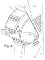
Damit wird das Lösen der Buchsenleiste 3 von der Stiftleiste 2 bzw. das Entriegeln von der Stiftleiste 2 unterstützt, vorzugsweise bis in eine Stellung, in welcher die Buchsenleiste 3 sich in einer nicht kontaktierten Stellung befindet und aus der Position der
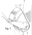
Nach
Zum Aufsetzen der Buchsenleiste 3 auf die Stiftleiste 1 wird der Entriegelungsbügel 5 in seine in dieser Darstellung untere Position bewegt - die Entriegelungsposition -, so dass die Buchsenleiste 3 auf die Stiftleiste 2 aufsteckbar und dort verrastbar ist.To place the
Sodann wird der Entriegelungsbügel 5 von Hand oder mit einem Schraubendreher in die Stellung der
Hierdurch wird eine Verriegelungsfunktion realisiert, da es nicht möglich ist, die Buchsenleiste 3 nach oben hin von der Stiftleiste 2 abzuziehen, da die obere Kante des Schlitzes dies verhindert. Ein Verrasten des Zapfens 13 in einer Aufweitung des Schlitzes oder dgl. ist optional denkbar (hier nicht dargestellt)...In this way, a locking function is realized, since it is not possible to pull the
Entriegelt wird diese Anordnung wiederum nach Art der
Anzumerken ist, dass bei einer Anordnung der Buchsenleiste am Elektronikgehäuse und einer hierauf aufrastbaren Stiftleiste die Anordnung des Entriegelungsbügels an der Stiftleiste vorgesehen sein kann, wobei die Funktion entsprechend umgekehrt wird.It should be noted that with an arrangement of the socket strip on the electronics housing and a pin strip that can be snapped onto it, the arrangement of the unlocking bracket on the pin strip can be provided, the function being reversed accordingly.
- ElektronikgehäuseElectronics housing
- 11
- StiftleistePin header
- 22nd
- Buchsen leisteSockets
- 33rd
- EntriegelungsvorrichtungUnlocking device
- 44th
- EntriegelungsbügelUnlocking bracket
- 5, 5'5, 5 '
- SchwenkachsenSwivel axes
- 66
- GrundschenkelBase leg
- 7a7a
- LängsschenkelLongitudinal leg
- 7b, c7b, c
- BetätigungskonturActuation contour
- 88th
- Schraubendreherscrewdriver
- 99
- EntriegelungskonturUnlocking contour
- 1010th
- AuflageflächeContact surface
- 1111
- Schlitzslot
- 1212
- ZapfenCones
- 1313
- BaubreiteOverall width
- X1, X2X1, X2
- AnreihrichtungBaying direction
- XX
- Pfeilarrow
- SS
Claims (4)
- A stackable housing arrangement, especially an electronic housing arrangement, comprising a housing, especially an electronic housing (1), wherein the housing is provided with at least one or several contact-pin strips and/or socket-pin strips, wherein the housing has a mounting width (X1) in the stacking direction, and comprising corresponding socket-pin strip (3) or contact-pin strip (2) of the housing arrangement which can respectively be inserted onto the at least one contact-pin strip (2) or socket-pin strip (3), wherein an unlocking apparatus (4) for unlocking the socket-pin strip (3) from the contact-pin strip (2) is provided, which unlocking apparatus is arranged on the insertable corresponding socket-pin strip or contact-pin strip (3, 2), wherein the entire overall mounting width (X2) of the corresponding contact-pin strip (2) or the corresponding socket-pin strip (3) with the unlocking apparatus (4) is not greater than the mounting width (X1) of the housing, especially the electronic housing (1), in the stacking direction, wherein the unlocking apparatus (4) is formed as a pivotable unlocking yoke (5) which is connected in an articulated manner to pivot pins (6) on opposite sides of the corresponding contact-pin strip (2) or the corresponding socket-pin strip (3), wherein the unlocking yoke (5) is provided with an unlocking contour (10) which extends eccentrically relative to the pivot pins (6) and which during unlocking rests in the manner of an abutment on the bearing surface (11) of the housing or the contact-pin strip, and wherein the unlocking yoke (5) is in alignment in the stacking direction with the electronic housing (1), and wherein the unlocking yoke (5) has a U-shape with a base leg (7a) and two side legs (7b, 7c).
- An electronic housing according to claim 1, wherein the unlocking yoke (5) engages around the socket-pin strip (3), and the base leg (7a) has an actuating contour (8).
- An electronic housing according to one of the preceding claims, wherein the unlocking apparatus (4) is combined with a locking device in the manner of a structural unit.
- An electronic housing according to one of the preceding claims, wherein the unlocking yoke (5) comprises at least one slot (12) which is formed to interact in a locking manner with a pin (13) on the contact-pin strip (1) or on the electronic housing.
Applications Claiming Priority (1)
| Application Number | Priority Date | Filing Date | Title |
|---|---|---|---|
| DE202008002111U DE202008002111U1 (en) | 2008-02-14 | 2008-02-14 | Bayable electronics housing with pin or socket strips |
Publications (4)
| Publication Number | Publication Date |
|---|---|
| EP2091312A2 EP2091312A2 (en) | 2009-08-19 |
| EP2091312A3 EP2091312A3 (en) | 2010-07-21 |
| EP2091312B1 EP2091312B1 (en) | 2017-03-22 |
| EP2091312B2 true EP2091312B2 (en) | 2020-06-10 |
Family
ID=40637015
Family Applications (1)
| Application Number | Title | Priority Date | Filing Date |
|---|---|---|---|
| EP09150924.0A Active EP2091312B2 (en) | 2008-02-14 | 2009-01-20 | Stackable electronics housing with multi-pin connector or female connector |
Country Status (7)
| Country | Link |
|---|---|
| US (1) | US7736161B2 (en) |
| EP (1) | EP2091312B2 (en) |
| JP (2) | JP2009193959A (en) |
| CN (1) | CN101521336A (en) |
| DE (1) | DE202008002111U1 (en) |
| DK (1) | DK2091312T4 (en) |
| ES (1) | ES2628510T5 (en) |
Families Citing this family (11)
| Publication number | Priority date | Publication date | Assignee | Title |
|---|---|---|---|---|
| EP2639895A1 (en) * | 2012-03-16 | 2013-09-18 | EATON Industries Manufacturing GmbH | Electrical plug retainer outlet |
| DE202012101639U1 (en) * | 2012-05-03 | 2013-08-06 | Weidmüller Interface GmbH & Co. KG | Through housing |
| DE102012105509B4 (en) | 2012-06-25 | 2018-04-05 | Wago Verwaltungsgesellschaft Mbh | Electronic equipment housing |
| DE202012104581U1 (en) * | 2012-11-26 | 2014-02-27 | Weidmüller Interface GmbH & Co. KG | Arrangement of two interlockable, in particular electrical, assemblies |
| US9455510B2 (en) * | 2013-01-15 | 2016-09-27 | Weidmueller Interface Gmbh & Co. Kg | Attachment having a module and an electronics atachment |
| US20150031232A1 (en) * | 2013-07-24 | 2015-01-29 | International Business Machines Corporation | Electronic component latch |
| DE102014115252A1 (en) * | 2014-10-20 | 2016-04-21 | Phoenix Contact Gmbh & Co. Kg | Electrical connector pair |
| JP2018018584A (en) * | 2016-07-25 | 2018-02-01 | 住友電装株式会社 | connector |
| JP2018018583A (en) * | 2016-07-25 | 2018-02-01 | 住友電装株式会社 | connector |
| JP6268620B1 (en) * | 2016-09-16 | 2018-01-31 | 住友電装株式会社 | Lever type connector |
| WO2021093923A1 (en) * | 2019-11-15 | 2021-05-20 | Linak A/S | Control unit |
Citations (4)
| Publication number | Priority date | Publication date | Assignee | Title |
|---|---|---|---|---|
| DE19737479A1 (en) † | 1997-08-28 | 1999-03-04 | Michael Dipl Ing Katzenberger | Tool for extracting multiple integrated circuit from pulse socket |
| US6056582A (en) † | 1997-07-01 | 2000-05-02 | Yazaki Corporation | Lever fitting connector |
| DE102004002737A1 (en) † | 2004-01-20 | 2005-08-11 | Wago Verwaltungsgesellschaft Mbh | Release mechanism e.g. for latched plug or socket part, has swivel mounted lever arranged on long-side of plug module recess |
| EP1592092A1 (en) † | 2004-04-28 | 2005-11-02 | Tyco Electronics AMP K.K. | Lever-type Connector |
Family Cites Families (9)
| Publication number | Priority date | Publication date | Assignee | Title |
|---|---|---|---|---|
| JPH07114951A (en) * | 1993-10-18 | 1995-05-02 | Amp Japan Ltd | Lever type connector |
| JP3865785B2 (en) * | 1996-12-02 | 2007-01-10 | 花王株式会社 | Surfactant composition |
| JP2001076811A (en) * | 1999-09-09 | 2001-03-23 | Sumitomo Wiring Syst Ltd | Lever connector |
| US20010034165A1 (en) | 2000-03-10 | 2001-10-25 | Landis John M. | Terminal block connector |
| JP3603760B2 (en) * | 2000-08-11 | 2004-12-22 | 住友電装株式会社 | Lever type connector |
| JP3964146B2 (en) * | 2001-03-22 | 2007-08-22 | 矢崎総業株式会社 | Lever fitting type connector |
| JP3952877B2 (en) | 2002-06-24 | 2007-08-01 | 松下電工株式会社 | Relay terminal block |
| DE10236397A1 (en) | 2002-08-08 | 2004-02-26 | Wieland Electric Gmbh | Electrical terminal for switchgear, has securing device for locking position of contact body when contact element is connected to switchgear |
| DE102005027824B4 (en) | 2005-06-15 | 2013-09-12 | Eaton Industries Gmbh | Electrical switching device with plug-in device |
-
2008
- 2008-02-14 DE DE202008002111U patent/DE202008002111U1/en not_active Expired - Lifetime
-
2009
- 2009-01-20 DK DK09150924.0T patent/DK2091312T4/en active
- 2009-01-20 EP EP09150924.0A patent/EP2091312B2/en active Active
- 2009-01-20 ES ES09150924T patent/ES2628510T5/en active Active
- 2009-01-27 JP JP2009015277A patent/JP2009193959A/en active Pending
- 2009-02-09 US US12/322,889 patent/US7736161B2/en active Active
- 2009-02-13 CN CN200910007449A patent/CN101521336A/en active Pending
-
2013
- 2013-12-06 JP JP2013252964A patent/JP2014089967A/en active Pending
Patent Citations (4)
| Publication number | Priority date | Publication date | Assignee | Title |
|---|---|---|---|---|
| US6056582A (en) † | 1997-07-01 | 2000-05-02 | Yazaki Corporation | Lever fitting connector |
| DE19737479A1 (en) † | 1997-08-28 | 1999-03-04 | Michael Dipl Ing Katzenberger | Tool for extracting multiple integrated circuit from pulse socket |
| DE102004002737A1 (en) † | 2004-01-20 | 2005-08-11 | Wago Verwaltungsgesellschaft Mbh | Release mechanism e.g. for latched plug or socket part, has swivel mounted lever arranged on long-side of plug module recess |
| EP1592092A1 (en) † | 2004-04-28 | 2005-11-02 | Tyco Electronics AMP K.K. | Lever-type Connector |
Also Published As
| Publication number | Publication date |
|---|---|
| EP2091312A2 (en) | 2009-08-19 |
| EP2091312A3 (en) | 2010-07-21 |
| DK2091312T3 (en) | 2017-07-10 |
| DE202008002111U1 (en) | 2009-06-25 |
| JP2009193959A (en) | 2009-08-27 |
| CN101521336A (en) | 2009-09-02 |
| JP2014089967A (en) | 2014-05-15 |
| ES2628510T5 (en) | 2021-03-04 |
| ES2628510T3 (en) | 2017-08-03 |
| US20090209122A1 (en) | 2009-08-20 |
| US7736161B2 (en) | 2010-06-15 |
| DK2091312T4 (en) | 2020-08-31 |
| EP2091312B1 (en) | 2017-03-22 |
Similar Documents
| Publication | Publication Date | Title |
|---|---|---|
| EP2091312B2 (en) | Stackable electronics housing with multi-pin connector or female connector | |
| EP1667286B1 (en) | Device for connection of two terminals with busbars | |
| EP2339701B1 (en) | Circuit board connector with locking device | |
| EP1742315B1 (en) | Modular housing for mounting on a support rail | |
| EP2839544B1 (en) | Test terminal block | |
| DE102017117509B4 (en) | Electric device | |
| EP2606534A1 (en) | Mounting rail and module latching system | |
| EP3586404B1 (en) | Spring-force connection and round plug-in connector with a large number of spring-force connections | |
| WO2013050239A1 (en) | Connecting device for connecting a conductor end | |
| EP2883284A1 (en) | Connection module | |
| EP1715547B1 (en) | Modular system with connecting bridge for an internal bus conductor | |
| EP1191643B1 (en) | Housing for an electronic apparatus | |
| EP3021421B1 (en) | Connection device for multi-conductor cables | |
| DE102006054647B4 (en) | Electrical connector coupling | |
| EP2425497B1 (en) | Fastening device for fastening a connector plug to a base housing | |
| EP2432089B1 (en) | Device combination for protecting against electrical surges | |
| EP0086954B1 (en) | Tool to extract an electronic drawer from its frame | |
| EP3210261B1 (en) | Electronic module | |
| EP2264470B1 (en) | Connection system for electricity meters | |
| WO2004006397A1 (en) | Support for module cases | |
| DE102006027014B4 (en) | female connector | |
| DE102004007740B4 (en) | Module board and separator bracket | |
| EP3627639B1 (en) | Sliding element for a mounting and latching mechanism | |
| EP4042708B1 (en) | Pull-off device for an overvoltage protection magazine | |
| EP1412645B1 (en) | Equipment design |
Legal Events
| Date | Code | Title | Description |
|---|---|---|---|
| PUAI | Public reference made under article 153(3) epc to a published international application that has entered the european phase |
Free format text: ORIGINAL CODE: 0009012 |
|
| AK | Designated contracting states |
Kind code of ref document: A2 Designated state(s): AT BE BG CH CY CZ DE DK EE ES FI FR GB GR HR HU IE IS IT LI LT LU LV MC MK MT NL NO PL PT RO SE SI SK TR |
|
| AX | Request for extension of the european patent |
Extension state: AL BA RS |
|
| PUAL | Search report despatched |
Free format text: ORIGINAL CODE: 0009013 |
|
| AK | Designated contracting states |
Kind code of ref document: A3 Designated state(s): AT BE BG CH CY CZ DE DK EE ES FI FR GB GR HR HU IE IS IT LI LT LU LV MC MK MT NL NO PL PT RO SE SI SK TR |
|
| AX | Request for extension of the european patent |
Extension state: AL BA RS |
|
| RIC1 | Information provided on ipc code assigned before grant |
Ipc: H01R 13/629 20060101ALI20100615BHEP Ipc: H05K 7/14 20060101ALI20100615BHEP Ipc: H01R 9/26 20060101ALI20100615BHEP Ipc: H05K 5/00 20060101AFI20090525BHEP Ipc: H01R 13/514 20060101ALI20100615BHEP |
|
| 17P | Request for examination filed |
Effective date: 20101122 |
|
| AKX | Designation fees paid |
Designated state(s): AT BE BG CH CY CZ DE DK EE ES FI FR GB GR HR HU IE IS IT LI LT LU LV MC MK MT NL NO PL PT RO SE SI SK TR |
|
| 17Q | First examination report despatched |
Effective date: 20130729 |
|
| GRAP | Despatch of communication of intention to grant a patent |
Free format text: ORIGINAL CODE: EPIDOSNIGR1 |
|
| INTG | Intention to grant announced |
Effective date: 20160928 |
|
| GRAJ | Information related to disapproval of communication of intention to grant by the applicant or resumption of examination proceedings by the epo deleted |
Free format text: ORIGINAL CODE: EPIDOSDIGR1 |
|
| GRAS | Grant fee paid |
Free format text: ORIGINAL CODE: EPIDOSNIGR3 |
|
| GRAP | Despatch of communication of intention to grant a patent |
Free format text: ORIGINAL CODE: EPIDOSNIGR1 |
|
| GRAA | (expected) grant |
Free format text: ORIGINAL CODE: 0009210 |
|
| INTC | Intention to grant announced (deleted) | ||
| INTG | Intention to grant announced |
Effective date: 20170206 |
|
| AK | Designated contracting states |
Kind code of ref document: B1 Designated state(s): AT BE BG CH CY CZ DE DK EE ES FI FR GB GR HR HU IE IS IT LI LT LU LV MC MK MT NL NO PL PT RO SE SI SK TR |
|
| REG | Reference to a national code |
Ref country code: GB Ref legal event code: FG4D Free format text: NOT ENGLISH |
|
| REG | Reference to a national code |
Ref country code: CH Ref legal event code: EP |
|
| REG | Reference to a national code |
Ref country code: AT Ref legal event code: REF Ref document number: 878885 Country of ref document: AT Kind code of ref document: T Effective date: 20170415 |
|
| REG | Reference to a national code |
Ref country code: IE Ref legal event code: FG4D Free format text: LANGUAGE OF EP DOCUMENT: GERMAN |
|
| REG | Reference to a national code |
Ref country code: DE Ref legal event code: R096 Ref document number: 502009013779 Country of ref document: DE |
|
| REG | Reference to a national code |
Ref country code: DK Ref legal event code: T3 Effective date: 20170704 |
|
| REG | Reference to a national code |
Ref country code: NL Ref legal event code: MP Effective date: 20170322 |
|
| PG25 | Lapsed in a contracting state [announced via postgrant information from national office to epo] |
Ref country code: GR Free format text: LAPSE BECAUSE OF FAILURE TO SUBMIT A TRANSLATION OF THE DESCRIPTION OR TO PAY THE FEE WITHIN THE PRESCRIBED TIME-LIMIT Effective date: 20170623 Ref country code: LT Free format text: LAPSE BECAUSE OF FAILURE TO SUBMIT A TRANSLATION OF THE DESCRIPTION OR TO PAY THE FEE WITHIN THE PRESCRIBED TIME-LIMIT Effective date: 20170322 Ref country code: FI Free format text: LAPSE BECAUSE OF FAILURE TO SUBMIT A TRANSLATION OF THE DESCRIPTION OR TO PAY THE FEE WITHIN THE PRESCRIBED TIME-LIMIT Effective date: 20170322 Ref country code: HR Free format text: LAPSE BECAUSE OF FAILURE TO SUBMIT A TRANSLATION OF THE DESCRIPTION OR TO PAY THE FEE WITHIN THE PRESCRIBED TIME-LIMIT Effective date: 20170322 Ref country code: NO Free format text: LAPSE BECAUSE OF FAILURE TO SUBMIT A TRANSLATION OF THE DESCRIPTION OR TO PAY THE FEE WITHIN THE PRESCRIBED TIME-LIMIT Effective date: 20170622 |
|
| REG | Reference to a national code |
Ref country code: ES Ref legal event code: FG2A Ref document number: 2628510 Country of ref document: ES Kind code of ref document: T3 Effective date: 20170803 |
|
| REG | Reference to a national code |
Ref country code: LT Ref legal event code: MG4D |
|
| PG25 | Lapsed in a contracting state [announced via postgrant information from national office to epo] |
Ref country code: SE Free format text: LAPSE BECAUSE OF FAILURE TO SUBMIT A TRANSLATION OF THE DESCRIPTION OR TO PAY THE FEE WITHIN THE PRESCRIBED TIME-LIMIT Effective date: 20170322 Ref country code: LV Free format text: LAPSE BECAUSE OF FAILURE TO SUBMIT A TRANSLATION OF THE DESCRIPTION OR TO PAY THE FEE WITHIN THE PRESCRIBED TIME-LIMIT Effective date: 20170322 Ref country code: BG Free format text: LAPSE BECAUSE OF FAILURE TO SUBMIT A TRANSLATION OF THE DESCRIPTION OR TO PAY THE FEE WITHIN THE PRESCRIBED TIME-LIMIT Effective date: 20170622 |
|
| PG25 | Lapsed in a contracting state [announced via postgrant information from national office to epo] |
Ref country code: NL Free format text: LAPSE BECAUSE OF FAILURE TO SUBMIT A TRANSLATION OF THE DESCRIPTION OR TO PAY THE FEE WITHIN THE PRESCRIBED TIME-LIMIT Effective date: 20170322 |
|
| PG25 | Lapsed in a contracting state [announced via postgrant information from national office to epo] |
Ref country code: CZ Free format text: LAPSE BECAUSE OF FAILURE TO SUBMIT A TRANSLATION OF THE DESCRIPTION OR TO PAY THE FEE WITHIN THE PRESCRIBED TIME-LIMIT Effective date: 20170322 Ref country code: EE Free format text: LAPSE BECAUSE OF FAILURE TO SUBMIT A TRANSLATION OF THE DESCRIPTION OR TO PAY THE FEE WITHIN THE PRESCRIBED TIME-LIMIT Effective date: 20170322 Ref country code: SK Free format text: LAPSE BECAUSE OF FAILURE TO SUBMIT A TRANSLATION OF THE DESCRIPTION OR TO PAY THE FEE WITHIN THE PRESCRIBED TIME-LIMIT Effective date: 20170322 Ref country code: RO Free format text: LAPSE BECAUSE OF FAILURE TO SUBMIT A TRANSLATION OF THE DESCRIPTION OR TO PAY THE FEE WITHIN THE PRESCRIBED TIME-LIMIT Effective date: 20170322 |
|
| PG25 | Lapsed in a contracting state [announced via postgrant information from national office to epo] |
Ref country code: IS Free format text: LAPSE BECAUSE OF FAILURE TO SUBMIT A TRANSLATION OF THE DESCRIPTION OR TO PAY THE FEE WITHIN THE PRESCRIBED TIME-LIMIT Effective date: 20170722 Ref country code: PL Free format text: LAPSE BECAUSE OF FAILURE TO SUBMIT A TRANSLATION OF THE DESCRIPTION OR TO PAY THE FEE WITHIN THE PRESCRIBED TIME-LIMIT Effective date: 20170322 Ref country code: PT Free format text: LAPSE BECAUSE OF FAILURE TO SUBMIT A TRANSLATION OF THE DESCRIPTION OR TO PAY THE FEE WITHIN THE PRESCRIBED TIME-LIMIT Effective date: 20170724 |
|
| REG | Reference to a national code |
Ref country code: DE Ref legal event code: R026 Ref document number: 502009013779 Country of ref document: DE |
|
| PLBI | Opposition filed |
Free format text: ORIGINAL CODE: 0009260 |
|
| PLAX | Notice of opposition and request to file observation + time limit sent |
Free format text: ORIGINAL CODE: EPIDOSNOBS2 |
|
| 26 | Opposition filed |
Opponent name: WAGO KONTAKTTECHNIK GMBH & CO. KG Effective date: 20171220 |
|
| PG25 | Lapsed in a contracting state [announced via postgrant information from national office to epo] |
Ref country code: SI Free format text: LAPSE BECAUSE OF FAILURE TO SUBMIT A TRANSLATION OF THE DESCRIPTION OR TO PAY THE FEE WITHIN THE PRESCRIBED TIME-LIMIT Effective date: 20170322 |
|
| PLBB | Reply of patent proprietor to notice(s) of opposition received |
Free format text: ORIGINAL CODE: EPIDOSNOBS3 |
|
| REG | Reference to a national code |
Ref country code: CH Ref legal event code: PL |
|
| PG25 | Lapsed in a contracting state [announced via postgrant information from national office to epo] |
Ref country code: MT Free format text: LAPSE BECAUSE OF FAILURE TO SUBMIT A TRANSLATION OF THE DESCRIPTION OR TO PAY THE FEE WITHIN THE PRESCRIBED TIME-LIMIT Effective date: 20170322 |
|
| PG25 | Lapsed in a contracting state [announced via postgrant information from national office to epo] |
Ref country code: FR Free format text: LAPSE BECAUSE OF NON-PAYMENT OF DUE FEES Effective date: 20180131 Ref country code: LU Free format text: LAPSE BECAUSE OF NON-PAYMENT OF DUE FEES Effective date: 20180120 |
|
| REG | Reference to a national code |
Ref country code: IE Ref legal event code: MM4A |
|
| REG | Reference to a national code |
Ref country code: FR Ref legal event code: ST Effective date: 20180928 |
|
| REG | Reference to a national code |
Ref country code: BE Ref legal event code: MM Effective date: 20180131 |
|
| PG25 | Lapsed in a contracting state [announced via postgrant information from national office to epo] |
Ref country code: CH Free format text: LAPSE BECAUSE OF NON-PAYMENT OF DUE FEES Effective date: 20180131 Ref country code: BE Free format text: LAPSE BECAUSE OF NON-PAYMENT OF DUE FEES Effective date: 20180131 Ref country code: LI Free format text: LAPSE BECAUSE OF NON-PAYMENT OF DUE FEES Effective date: 20180131 |
|
| PG25 | Lapsed in a contracting state [announced via postgrant information from national office to epo] |
Ref country code: IE Free format text: LAPSE BECAUSE OF NON-PAYMENT OF DUE FEES Effective date: 20180120 |
|
| REG | Reference to a national code |
Ref country code: AT Ref legal event code: MM01 Ref document number: 878885 Country of ref document: AT Kind code of ref document: T Effective date: 20180120 |
|
| PG25 | Lapsed in a contracting state [announced via postgrant information from national office to epo] |
Ref country code: AT Free format text: LAPSE BECAUSE OF NON-PAYMENT OF DUE FEES Effective date: 20180120 |
|
| PG25 | Lapsed in a contracting state [announced via postgrant information from national office to epo] |
Ref country code: MC Free format text: LAPSE BECAUSE OF FAILURE TO SUBMIT A TRANSLATION OF THE DESCRIPTION OR TO PAY THE FEE WITHIN THE PRESCRIBED TIME-LIMIT Effective date: 20170322 |
|
| PG25 | Lapsed in a contracting state [announced via postgrant information from national office to epo] |
Ref country code: TR Free format text: LAPSE BECAUSE OF FAILURE TO SUBMIT A TRANSLATION OF THE DESCRIPTION OR TO PAY THE FEE WITHIN THE PRESCRIBED TIME-LIMIT Effective date: 20170322 |
|
| PUAH | Patent maintained in amended form |
Free format text: ORIGINAL CODE: 0009272 |
|
| STAA | Information on the status of an ep patent application or granted ep patent |
Free format text: STATUS: PATENT MAINTAINED AS AMENDED |
|
| PG25 | Lapsed in a contracting state [announced via postgrant information from national office to epo] |
Ref country code: HU Free format text: LAPSE BECAUSE OF FAILURE TO SUBMIT A TRANSLATION OF THE DESCRIPTION OR TO PAY THE FEE WITHIN THE PRESCRIBED TIME-LIMIT; INVALID AB INITIO Effective date: 20090120 |
|
| 27A | Patent maintained in amended form |
Effective date: 20200610 |
|
| AK | Designated contracting states |
Kind code of ref document: B2 Designated state(s): AT BE BG CH CY CZ DE DK EE ES FI FR GB GR HR HU IE IS IT LI LT LU LV MC MK MT NL NO PL PT RO SE SI SK TR |
|
| REG | Reference to a national code |
Ref country code: DE Ref legal event code: R102 Ref document number: 502009013779 Country of ref document: DE |
|
| PG25 | Lapsed in a contracting state [announced via postgrant information from national office to epo] |
Ref country code: CY Free format text: LAPSE BECAUSE OF FAILURE TO SUBMIT A TRANSLATION OF THE DESCRIPTION OR TO PAY THE FEE WITHIN THE PRESCRIBED TIME-LIMIT Effective date: 20170322 Ref country code: MK Free format text: LAPSE BECAUSE OF NON-PAYMENT OF DUE FEES Effective date: 20170322 |
|
| REG | Reference to a national code |
Ref country code: DK Ref legal event code: T4 Effective date: 20200828 |
|
| REG | Reference to a national code |
Ref country code: ES Ref legal event code: DC2A Ref document number: 2628510 Country of ref document: ES Kind code of ref document: T5 Effective date: 20210304 |
|
| PGFP | Annual fee paid to national office [announced via postgrant information from national office to epo] |
Ref country code: ES Payment date: 20230330 Year of fee payment: 15 Ref country code: DK Payment date: 20230123 Year of fee payment: 15 |
|
| PGFP | Annual fee paid to national office [announced via postgrant information from national office to epo] |
Ref country code: IT Payment date: 20230120 Year of fee payment: 15 Ref country code: GB Payment date: 20230119 Year of fee payment: 15 Ref country code: DE Payment date: 20230123 Year of fee payment: 15 |
|
| P01 | Opt-out of the competence of the unified patent court (upc) registered |
Effective date: 20230524 |
|
| PGFP | Annual fee paid to national office [announced via postgrant information from national office to epo] |
Ref country code: ES Payment date: 20240223 Year of fee payment: 16 |