EP2087981A1 - Master and microreactor - Google Patents
Master and microreactor Download PDFInfo
- Publication number
- EP2087981A1 EP2087981A1 EP07830161A EP07830161A EP2087981A1 EP 2087981 A1 EP2087981 A1 EP 2087981A1 EP 07830161 A EP07830161 A EP 07830161A EP 07830161 A EP07830161 A EP 07830161A EP 2087981 A1 EP2087981 A1 EP 2087981A1
- Authority
- EP
- European Patent Office
- Prior art keywords
- master
- groove
- substrate
- molding die
- section
- Prior art date
- Legal status (The legal status is an assumption and is not a legal conclusion. Google has not performed a legal analysis and makes no representation as to the accuracy of the status listed.)
- Withdrawn
Links
Images



Classifications
-
- B—PERFORMING OPERATIONS; TRANSPORTING
- B29—WORKING OF PLASTICS; WORKING OF SUBSTANCES IN A PLASTIC STATE IN GENERAL
- B29C—SHAPING OR JOINING OF PLASTICS; SHAPING OF MATERIAL IN A PLASTIC STATE, NOT OTHERWISE PROVIDED FOR; AFTER-TREATMENT OF THE SHAPED PRODUCTS, e.g. REPAIRING
- B29C33/00—Moulds or cores; Details thereof or accessories therefor
- B29C33/42—Moulds or cores; Details thereof or accessories therefor characterised by the shape of the moulding surface, e.g. ribs or grooves
-
- B—PERFORMING OPERATIONS; TRANSPORTING
- B29—WORKING OF PLASTICS; WORKING OF SUBSTANCES IN A PLASTIC STATE IN GENERAL
- B29C—SHAPING OR JOINING OF PLASTICS; SHAPING OF MATERIAL IN A PLASTIC STATE, NOT OTHERWISE PROVIDED FOR; AFTER-TREATMENT OF THE SHAPED PRODUCTS, e.g. REPAIRING
- B29C33/00—Moulds or cores; Details thereof or accessories therefor
- B29C33/38—Moulds or cores; Details thereof or accessories therefor characterised by the material or the manufacturing process
- B29C33/3842—Manufacturing moulds, e.g. shaping the mould surface by machining
- B29C33/3857—Manufacturing moulds, e.g. shaping the mould surface by machining by making impressions of one or more parts of models, e.g. shaped articles and including possible subsequent assembly of the parts
- B29C33/3878—Manufacturing moulds, e.g. shaping the mould surface by machining by making impressions of one or more parts of models, e.g. shaped articles and including possible subsequent assembly of the parts used as masters for making successive impressions
-
- B—PERFORMING OPERATIONS; TRANSPORTING
- B81—MICROSTRUCTURAL TECHNOLOGY
- B81C—PROCESSES OR APPARATUS SPECIALLY ADAPTED FOR THE MANUFACTURE OR TREATMENT OF MICROSTRUCTURAL DEVICES OR SYSTEMS
- B81C99/00—Subject matter not provided for in other groups of this subclass
- B81C99/0075—Manufacture of substrate-free structures
- B81C99/0085—Manufacture of substrate-free structures using moulds and master templates, e.g. for hot-embossing
-
- B—PERFORMING OPERATIONS; TRANSPORTING
- B81—MICROSTRUCTURAL TECHNOLOGY
- B81B—MICROSTRUCTURAL DEVICES OR SYSTEMS, e.g. MICROMECHANICAL DEVICES
- B81B2201/00—Specific applications of microelectromechanical systems
- B81B2201/05—Microfluidics
- B81B2201/051—Micromixers, microreactors
Definitions
- the present invention relates to a master that represents a mother body for a molding die and to a microreactor produced by the master.
- a microreactor is used to inspect reactions and changes in liquid samples which are different in terms of a type and are mixed in a microscopic flow channel.
- the microreactor is generally constituted of glass or the like in many cases, it is also possible to produce it through injection molding by using a molding die.
- Patent Literature 1 An example of a manufacturing method for the aforesaid molding die is disclosed in Patent Literature 1.
- a master which is a mother body for the die and has recess and projection forms which are the same as those of a resin molded product
- a molding die is produced by the master through electrocasting processing or the like, and in particular, mold releasability of molding die from the master is improved by forming a specific conductive film on a surface of the master (11th line in lower paragraph on the right side on page 3 - 11th line in upper paragraph on the left side on page 4).
- projection portion 111 of molding die 110 may be deformed by the influence of a shape of recess portion 101 (undercut form) or by an error of squareness and straightness during releasing or is chipped by the influence of releasing resistance with the recess portion 101, when the molding die 110 is released from the master 100, because the recess portion 101 is in a rectangular shape.
- the projection portion 111 of the molding die 110 is made in the rectangular form as shown in Fig. 7(b) according to the recess portion 101 of the master 100, and resin molded product 120 has also a possibility to be deformed when resin molded product 120 is released from the molding die 110.
- An objective of the invention is to improve mold releasability between the master and the molding die.
- the first invention to solve the aforesaid problem is a master to be a mother body for a molding die wherein the master has grooves corresponding to flow channels of resin molded product, and a cross-section of the grooves is curved or is bent.
- a cross-section of a bottom surface portion of the aforesaid groove may also be in the form of a curved surface, or a cross-section of a side surface portion of the aforesaid groove may also be in the form of a slope or in the form of a curved surface.
- a bottom surface portion and a side surface portion of the aforesaid groove may also be in the form of a semicircle, or a corner portion of the aforesaid groove may also be in the form of a curved surface.
- a cross-section of a bottom surface portion in the lengthwise direction of the aforesaid groove may also be in the form of a step, the form of a slope or the form of a curved surface, or a cross-section of an edge portion of the aforesaid groove may also be in the form of a curved surface, a slope or a step.
- the second invention is a microreactor that has a substrate and a covering body that covers the substrate both of which are bonded together wherein the aforesaid substrate is produced with a master described in any one of Claims 1 - 7.
- a cross-section of the groove of the master is curved or bent, which prevents a projection portion of the molding die, when the molding die is released from the master, from being deformed due to a shape of a groove on the master and an error of squareness and straightness during the releasing and from being chipped by an influence of resistance for the releasing from grooves of the master, thus, mold releasability of the molding die from the master can be improved.
- flow channels identical to the grooves of the master in terms of a shape are formed on the substrate, and when the flow channels are in forms described in Claims 2 - 6 in particular, it is possible to control the flow velocity of liquid samples which flow through the flow channels without changing a width of the flow channels.
- a flow channel of the substrate is in a form that is described in Claim 7, it is possible to prevent excessive resin components and adhesives from being infiltrated into the flow channel, when thermal adhesion technology and adhesives are used for gluing a substrate and a covering body together.
- microreactor 1 has therein substrate 2 and covering body 3 each of which is in the form of a rectangular parallelepiped substantially.
- the substrate 2 and the covering body 3 are made of resin, and the covering body 3 is pasted on the substrate 2.
- inflow channels 21 and 22, reaction flow channel 23, and outflow channels 24 and 25 are formed on a surface of the substrate 2.
- an end portion on one side of reaction flow channel 23 is connected, and to the end portion on the other side of reaction flow channel 23, the merging section for the outflow channels 24 and 25 is connected.
- These inflow channels 21 and 22, reaction flow channel 23 and outflow channels 24 and 25 are grooves (micro flow channels) which are extremely microscopic.
- Inflow entrances 31 and 32 and outflow exits 34 and 35 are formed on the covering body 3.
- the inflow entrances 31 and 32 are communicated respectively with the inflow channels 21 and 22, while, the outflow channels 34 and 35 are communicated respectively with the outflow channels 24 and 25.
- respective liquids flow through the inflow channels 21 and 22 to be merged, and are mixed in the reaction flow channel 23 to be branched to outflow channels 24 and 25, to flow out of the outflow exits 34 an 35.
- microreactor 1 is used favorably for mixing liquid samples such as blood and medicines which are different each other in terms of types.
- master 40 is a mother body of a molding die for substrate 2 of microreactor 1, and it has master blank 41 that is in the shape of a rectangular parallelepiped substantially.
- groove 41a is formed along the outer circumference of the master blank 41.
- Plated layer 42 is formed on the master blank 41 to hold the master blank 41 from one side surface to the other side surface thereof, and groove 43 is formed on the plated layer 42.
- the groove 43 corresponds to inflow channels 21 and 22, reaction flow channel 23, and outflow channels 24 and 25, and it is a groove formed by machining process and is extremely microscopic.
- bottom surface portion 43a of the groove 43 is in the shape of a curved surface, and it is of the structure in which the molding die can easily be released from the master 40.
- the bottom surface portion 43a may also be in the form of another curved surface that is different from Fig. 2 as shown in Fig. 3(a)
- side surface portion 43b may also be in the form of a slope as shown in Fig. 3(b)
- the side surface portion 43b may also be in the form of a curved surface as shown in Figs. 3(c) and 3(d)
- the bottom surface portion 43a and the side surface portion 43b may also be in the form of a hemisphere face as shown in Fig. 3(e)
- corner portion 43c may also be in the form of a curved surface as shown in Fig.
- the bottom surface portion 43a may also be in the form of a step, or of a slope or of a curved surface in its length direction as shown in Fig. 3(g) .
- an angle formed by side surface portion 43b and the perpendicular line is about 0 - 10°
- a radius of curvature on corner portion 43c is about 0.02 - 10 ⁇ m.
- edge portion 43d may also be in the form of a curved surface as shown in Fig. 4(a)
- edge portion 43d may also be in the form of a slope as shown in Fig. 4(b)
- edge portion 43d may also be in the form of a step as shown in Fig. 4(c) .
- the shape of the groove 43 may also be a combination of respective shapes shown in Fig. 2 - Fig. 4 properly, and a cross-section of the groove 43 has only to be curved or bent, eventually.
- each of grooves 43 shown in Fig. 2 , Figs. 3(a) - 3(f) and Figs. 4(a) - 4(c) indicates a shape after cutting in the direction perpendicular to the lengthwise direction of each groove
- groove 43 shown in Fig. 3(g) indicates a shape after cutting in the lengthwise direction of the groove.
- the manufacturing method includes manufacturing of a molding die from master 40, manufacturing of substrate 2 by forming resins with the molding die and gluing together of the substrate 2 and covering body 3.
- the substrate 2 is produced from master 40.
- master blank 41 shown in Fig. 5(a) is prepared.
- plated layer 42 is formed by conducting Ni-P plating processing and Cu plating processing on the master blank 41 as shown in Fig. 5(b) .
- the plated layer 42 is formed to hold master blank 41 from one side surface to the other side surface of master blank 41 owing to groove 41a, so that the master blank 41 and the plated layer 42 hardly peel off each other.
- machining process is conducted on the top surface of the plated layer 42, and groove 43 is formed to complete master 40.
- the master 40 is a mother body of the molding die of substrate 2, and the groove 43 corresponds to inflow channels 21 and 22, reaction flow channel 23 and outflow channels 24 and 25 of the substrate 2.
- the plated layer 42 does not need to be on the master 40, and for example, it is possible to prepare master blank 41 by using a homogeneous material such as aluminum alloy or oxygen-free copper as a material so that the master blank 41 may serve as master 40.
- an oxide film (not shown) is formed on top of the plated layer 42 of master 40, and electrocasting processing is conducted on top of the oxide film to form thick electrocasting processed object 50 so that the plated layer 42 may be covered thereby.
- the reason of forming the oxide film on top of the plated layer 42 before electrocasting processing is to make the electrocasting processed object 50 to be released easily from the master 40.
- an outer shape of the electrocasting processed object 50 is applied with machining process additionally, as is shown by arrow A in Fig. 5(e) , and the lateral of the electrocasting processed object 50 is removed until the moment when the lateral side of the electrocasting processed object 50 is aligned with the lateral side of the master 40 (plated layer 42).
- the electrocasting processed object 50 which has been processed by machining additionally is released from the master 40, and the aforesaid oxide film interposed between a bottom surface (transfer surface) of the electrocasting processed object 50 and an upper surface of the plated layer 42 of the master 40 is removed.
- molding die 52 equipped with projection portion 51 corresponding to the groove 43 of the master 40 can be produced.
- the molding die 52 is mounted on a base mold.
- the molding die 52 can be mounted on the base mold by means of adhesives, screw cramp, cramp fixing or suction and others.
- substrate 2 is produced from a resin such as thermoplastic resin through injection molding on the molding die 52, and finally, the substrate 2 and covering body 3 are glued together through thermofusion or by adhesives, thus, microreactor 1 can be produced.
- bottom surface portion 43a of groove 43 of the master 40 is in the form of a curved surface. Therefore, when the electrocasting processed object 50 is released from the master 40, it is possible to prevent projection portion 51 of the electrocasting processed object 50 from being deformed because of the shape of groove 43 of the master 40 or an error of squareness and straightness in the releasing, or from being chipped by an influence of releasing resistance against groove 43 of the master 40, thus, mold releasability between the master 40 and molding die 52 can be improved.
- groove 43 of master 40 When forming groove 43 of master 40, machining process is conducted on the plated layer 42, whereby, the degree of freedom for microscopic processing is greater than that in the case of forming the groove 43 through photolithography and etching, which eliminates the need for a clean room, a UV cut room and wastewater-treatment equipment which are needed in the case of photolithography and etching.
- each of the forms of inflow channels 21 and 22, reaction flow channel 23 and outflow channels 24 and 25 on substrate 2 is the same as that of the groove 43 of the master 40. Therefore, if groove 43 having the form in Fig. 2 - Fig. 3 is formed on the plated layer 42, it is possible to control the flow velocity of liquid samples which flow through the inflow channels 21 and 22, the reaction flow channel 23 and the outflow channels 24 and 25, without changing a width of the flow channel, and it is possible to cause the inflow channels 21 and 22, the reaction flow channel 23 and the outflow channels 24 and 25 to function effectively for uniform circulation, mixing and branching of the liquid samples.
- a form of flow channel that is suitable for changing the flow velocity at an inflow section, a mixing section or an outflow section for the liquid samples, suitable for generating a turbulent flow and a laminar flow on purpose or suitable for adding various functions such as lens function and a micro-pump function partially can be created.
Landscapes
- Engineering & Computer Science (AREA)
- Manufacturing & Machinery (AREA)
- Mechanical Engineering (AREA)
- Microelectronics & Electronic Packaging (AREA)
- Moulds For Moulding Plastics Or The Like (AREA)
- Automatic Analysis And Handling Materials Therefor (AREA)
- Micromachines (AREA)
- Physical Or Chemical Processes And Apparatus (AREA)
Abstract
Description
- The present invention relates to a master that represents a mother body for a molding die and to a microreactor produced by the master.
- In recent years, in the testing field such as a blood test, a microreactor is used to inspect reactions and changes in liquid samples which are different in terms of a type and are mixed in a microscopic flow channel. Though the microreactor is generally constituted of glass or the like in many cases, it is also possible to produce it through injection molding by using a molding die.
- An example of a manufacturing method for the aforesaid molding die is disclosed in Patent Literature 1. In the technology disclosed in Patent Literature 1, a master (which is a mother body for the die and has recess and projection forms which are the same as those of a resin molded product) is produced through photolithography and etching, and a molding die is produced by the master through electrocasting processing or the like, and in particular, mold releasability of molding die from the master is improved by forming a specific conductive film on a surface of the master (11th line in lower paragraph on the right side on page 3 - 11th line in upper paragraph on the left side on page 4).
- Patent Literature 1: Unexamined Japanese Patent Application Publication No.
4-195941 - However, in the technology disclosed in Patent Literature 1 wherein
recess portion 101 is formed on themaster 100 as is shown inFig. 7(a) ,projection portion 111 ofmolding die 110 may be deformed by the influence of a shape of recess portion 101 (undercut form) or by an error of squareness and straightness during releasing or is chipped by the influence of releasing resistance with therecess portion 101, when themolding die 110 is released from themaster 100, because therecess portion 101 is in a rectangular shape. In addition, theprojection portion 111 of themolding die 110 is made in the rectangular form as shown inFig. 7(b) according to therecess portion 101 of themaster 100, and resin moldedproduct 120 has also a possibility to be deformed when resin moldedproduct 120 is released from themolding die 110. - An objective of the invention is to improve mold releasability between the master and the molding die.
- The first invention to solve the aforesaid problem is a master to be a mother body for a molding die wherein the master has grooves corresponding to flow channels of resin molded product, and a cross-section of the grooves is curved or is bent.
- In the master relating to the first invention, a cross-section of a bottom surface portion of the aforesaid groove may also be in the form of a curved surface, or a cross-section of a side surface portion of the aforesaid groove may also be in the form of a slope or in the form of a curved surface. A bottom surface portion and a side surface portion of the aforesaid groove may also be in the form of a semicircle, or a corner portion of the aforesaid groove may also be in the form of a curved surface. Further, a cross-section of a bottom surface portion in the lengthwise direction of the aforesaid groove may also be in the form of a step, the form of a slope or the form of a curved surface, or a cross-section of an edge portion of the aforesaid groove may also be in the form of a curved surface, a slope or a step.
- The second invention is a microreactor that has a substrate and a covering body that covers the substrate both of which are bonded together wherein the aforesaid substrate is produced with a master described in any one of Claims 1 - 7.
- In the first invention, a cross-section of the groove of the master is curved or bent, which prevents a projection portion of the molding die, when the molding die is released from the master, from being deformed due to a shape of a groove on the master and an error of squareness and straightness during the releasing and from being chipped by an influence of resistance for the releasing from grooves of the master, thus, mold releasability of the molding die from the master can be improved.
- In the second invention, flow channels identical to the grooves of the master in terms of a shape are formed on the substrate, and when the flow channels are in forms described in Claims 2 - 6 in particular, it is possible to control the flow velocity of liquid samples which flow through the flow channels without changing a width of the flow channels. On the other hand, when a flow channel of the substrate is in a form that is described in Claim 7, it is possible to prevent excessive resin components and adhesives from being infiltrated into the flow channel, when thermal adhesion technology and adhesives are used for gluing a substrate and a covering body together.
-
-
Fig. 1 is a perspective view showing a schematic structure of microreactor 1. -
Fig. 2 is a sectional view showing a schematic structure ofmaster 40. -
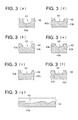
Fig. 3 is a sectional view showing an example of a variation ofgroove 43. -
Fig. 4 is a sectional view showing an example of a variation ofgroove 43. -
Fig. 5 is a diagram showing a process of a part of a manufacturing method for microreactor 1. -
Fig. 6 is a diagram for illustrating specific effects offered by a shape ofsubstrate 2 of microreactor 1. -
Fig. 7 is a diagram for illustrating problems in the prior art. -
- 1. Microreactor
- 2. Substrate
- 21, 22. Inflow channel
- 23. Reaction flow channel
- 24, 25. Outflow channel
- 3. Covering body
- 31, 32. Inflow channel
- 34, 35. Outflow channel
- 40. Master
- 41. Master blank
- 42. Plated layer
- 43. Groove
- 43a. Bottom surface portion
- 43b. Side surface portion
- 43c. Corner portion
- 43d. Edge portion
- The best mode for carrying out the present invention will be described as follows, referring to the drawings. However, various types of limitations which are preferable technically for carrying out the invention are given in the embodiments which will be described below, and the scope of the invention is not limited to the following embodiments and to the following illustrated examples.
- First, "a microreactor" and "a master" relating to the invention will be described, referring to
Fig. 1 - Fig. 3 . - As shown in
Fig. 1 , microreactor 1 has thereinsubstrate 2 and coveringbody 3 each of which is in the form of a rectangular parallelepiped substantially. Thesubstrate 2 and the coveringbody 3 are made of resin, and the coveringbody 3 is pasted on thesubstrate 2. - As shown by dotted lines in
Fig. 1 , on a surface of thesubstrate 2,inflow channels reaction flow channel 23, andoutflow channels inflow channels reaction flow channel 23 is connected, and to the end portion on the other side ofreaction flow channel 23, the merging section for theoutflow channels inflow channels reaction flow channel 23 andoutflow channels - Inflow entrances 31 and 32 and outflow exits 34 and 35 are formed on the covering
body 3. The inflow entrances 31 and 32 are communicated respectively with theinflow channels outflow channels outflow channels inflow channels reaction flow channel 23 to be branched tooutflow channels - As is shown in
Fig. 2 ,master 40 is a mother body of a molding die forsubstrate 2 of microreactor 1, and it has master blank 41 that is in the shape of a rectangular parallelepiped substantially. On themaster blank 41,groove 41a is formed along the outer circumference of themaster blank 41. Platedlayer 42 is formed on themaster blank 41 to hold the master blank 41 from one side surface to the other side surface thereof, andgroove 43 is formed on the platedlayer 42. Thegroove 43 corresponds toinflow channels reaction flow channel 23, andoutflow channels - As is shown by an enlarged diagram in
Fig. 2 ,bottom surface portion 43a of thegroove 43 is in the shape of a curved surface, and it is of the structure in which the molding die can easily be released from themaster 40. - With respect to the
groove 43, (1) thebottom surface portion 43a may also be in the form of another curved surface that is different fromFig. 2 as shown inFig. 3(a) , (2)side surface portion 43b may also be in the form of a slope as shown inFig. 3(b) , (3) theside surface portion 43b may also be in the form of a curved surface as shown inFigs. 3(c) and 3(d) , (4) thebottom surface portion 43a and theside surface portion 43b may also be in the form of a hemisphere face as shown inFig. 3(e) , (5)corner portion 43c may also be in the form of a curved surface as shown inFig. 3(f) , (6) thebottom surface portion 43a may also be in the form of a step, or of a slope or of a curved surface in its length direction as shown inFig. 3(g) . When thegroove 43 has the cross-sectional form shown inFig. 3(b) , it is preferable that an angle formed byside surface portion 43b and the perpendicular line is about 0 - 10°, and when thegroove 43 has the cross-sectional form shown inFig. 3(f) , it is preferable that a radius of curvature oncorner portion 43c is about 0.02 - 10 µm. - With respect to the
groove 43,edge portion 43d may also be in the form of a curved surface as shown inFig. 4(a) ,edge portion 43d may also be in the form of a slope as shown inFig. 4(b) andedge portion 43d may also be in the form of a step as shown inFig. 4(c) . - The shape of the
groove 43 may also be a combination of respective shapes shown inFig. 2 - Fig. 4 properly, and a cross-section of thegroove 43 has only to be curved or bent, eventually. - Meanwhile, each of
grooves 43 shown inFig. 2 ,Figs. 3(a) - 3(f) andFigs. 4(a) - 4(c) indicates a shape after cutting in the direction perpendicular to the lengthwise direction of each groove, and groove 43 shown inFig. 3(g) indicates a shape after cutting in the lengthwise direction of the groove. - Next, "a manufacturing method for a microreactor" relating to the invention will be described as follows, referring to
Fig. 5 . - Roughly speaking, the manufacturing method includes manufacturing of a molding die from
master 40, manufacturing ofsubstrate 2 by forming resins with the molding die and gluing together of thesubstrate 2 and coveringbody 3. In other words, thesubstrate 2 is produced frommaster 40. Each process of the manufacturing method will be described in detail as follows. - First, master blank 41 shown in
Fig. 5(a) is prepared. After that, platedlayer 42 is formed by conducting Ni-P plating processing and Cu plating processing on themaster blank 41 as shown inFig. 5(b) . The platedlayer 42 is formed to hold master blank 41 from one side surface to the other side surface of master blank 41 owing togroove 41a, so that themaster blank 41 and the platedlayer 42 hardly peel off each other. - After that, as is shown in
Fig. 5(c) , machining process is conducted on the top surface of the platedlayer 42, andgroove 43 is formed to completemaster 40. Themaster 40 is a mother body of the molding die ofsubstrate 2, and thegroove 43 corresponds toinflow channels reaction flow channel 23 andoutflow channels substrate 2. - Incidentally, the plated
layer 42 does not need to be on themaster 40, and for example, it is possible to prepare master blank 41 by using a homogeneous material such as aluminum alloy or oxygen-free copper as a material so that themaster blank 41 may serve asmaster 40. - After that, as is shown in
Fig. 5(d) , an oxide film (not shown) is formed on top of the platedlayer 42 ofmaster 40, and electrocasting processing is conducted on top of the oxide film to form thick electrocasting processedobject 50 so that the platedlayer 42 may be covered thereby. The reason of forming the oxide film on top of the platedlayer 42 before electrocasting processing is to make the electrocasting processedobject 50 to be released easily from themaster 40. - After that, under the condition that the electrocasting processed
object 50 is not released from themaster 40, an outer shape of the electrocasting processedobject 50 is applied with machining process additionally, as is shown by arrow A inFig. 5(e) , and the lateral of the electrocasting processedobject 50 is removed until the moment when the lateral side of the electrocasting processedobject 50 is aligned with the lateral side of the master 40 (plated layer 42). - After that, as is shown by arrow B in
Fig. 5(e) , the electrocasting processedobject 50 which has been processed by machining additionally is released from themaster 40, and the aforesaid oxide film interposed between a bottom surface (transfer surface) of the electrocasting processedobject 50 and an upper surface of the platedlayer 42 of themaster 40 is removed. As a result, molding die 52 equipped withprojection portion 51 corresponding to thegroove 43 of themaster 40 can be produced. - Afterwards, the molding die 52 is mounted on a base mold. The molding die 52 can be mounted on the base mold by means of adhesives, screw cramp, cramp fixing or suction and others.
- After that,
substrate 2 is produced from a resin such as thermoplastic resin through injection molding on the molding die 52, and finally, thesubstrate 2 and coveringbody 3 are glued together through thermofusion or by adhesives, thus, microreactor 1 can be produced. - In the aforesaid present embodiment,
bottom surface portion 43a ofgroove 43 of themaster 40 is in the form of a curved surface. Therefore, when the electrocasting processedobject 50 is released from themaster 40, it is possible to preventprojection portion 51 of the electrocasting processedobject 50 from being deformed because of the shape ofgroove 43 of themaster 40 or an error of squareness and straightness in the releasing, or from being chipped by an influence of releasing resistance againstgroove 43 of themaster 40, thus, mold releasability between themaster 40 and molding die 52 can be improved. - When forming
groove 43 ofmaster 40, machining process is conducted on the platedlayer 42, whereby, the degree of freedom for microscopic processing is greater than that in the case of forming thegroove 43 through photolithography and etching, which eliminates the need for a clean room, a UV cut room and wastewater-treatment equipment which are needed in the case of photolithography and etching. - Further, in the present embodiment, each of the forms of
inflow channels reaction flow channel 23 andoutflow channels substrate 2 is the same as that of thegroove 43 of themaster 40. Therefore, ifgroove 43 having the form inFig. 2 - Fig. 3 is formed on the platedlayer 42, it is possible to control the flow velocity of liquid samples which flow through theinflow channels reaction flow channel 23 and theoutflow channels inflow channels reaction flow channel 23 and theoutflow channels - On the other hand, if
groove 43 having the form inFig. 4 is formed on the platedlayer 42, when thermofusion or a adhesive is used for the adhesion ofsubstrate 2 and coveringbody 3, excessive resin components or adhesives is collected on the edge portion (corresponding to edgeportion 43d inFig. 4 ) wheresubstrate 2 comes into contact with coveringbody 3, as is shown inFigs. 6(a) - 6(c) , and the excessive resin components or adhesives can be prevented from intruding into theinflow channels reaction flow channel 23 and theoutflow channels
Claims (8)
- A master which is a mother body of a molding die, the master comprising:a groove corresponding to a flow channel of a resin molded product,wherein a cross section of the groove is curved or bent.
- The master of claim 1,
wherein a cross section of a bottom surface portion of the groove is in a form of a curved surface. - The master of claim 1,
wherein a cross section of a side surface portion of the groove is in a form of a slope or a curved surface. - The master of claim 1,
wherein a bottom surface portion and a side surface portion of the groove are in a form of a semicircle. - The master of claim 1,
wherein a corner portion of the groove is in a form of a curved surface. - The master of any one of claims 1 - 5,
wherein a cross section of a bottom surface portion in a lengthwise direction of the groove is in a form of a step, a slope or a curved surface. - The master of any one of claims 1 - 6,
wherein a cross section of an edge portion of the groove is in a form of a curved surface, a slope or a step. - A microreactor comprising:a substrate;a covering body which covers the substrate,wherein the substrate and the covering body are bonded together, and
wherein the substrate is made by the master of any one of claims 1 - 7,
Applications Claiming Priority (2)
| Application Number | Priority Date | Filing Date | Title |
|---|---|---|---|
| JP2006296297 | 2006-10-31 | ||
| PCT/JP2007/070427 WO2008053720A1 (en) | 2006-10-31 | 2007-10-19 | Master and microreactor |
Publications (2)
| Publication Number | Publication Date |
|---|---|
| EP2087981A1 true EP2087981A1 (en) | 2009-08-12 |
| EP2087981A4 EP2087981A4 (en) | 2013-01-02 |
Family
ID=39344063
Family Applications (1)
| Application Number | Title | Priority Date | Filing Date |
|---|---|---|---|
| EP07830161A Withdrawn EP2087981A4 (en) | 2006-10-31 | 2007-10-19 | Master and microreactor |
Country Status (4)
| Country | Link |
|---|---|
| US (1) | US20100074815A1 (en) |
| EP (1) | EP2087981A4 (en) |
| JP (1) | JPWO2008053720A1 (en) |
| WO (1) | WO2008053720A1 (en) |
Families Citing this family (4)
| Publication number | Priority date | Publication date | Assignee | Title |
|---|---|---|---|---|
| JP5303976B2 (en) * | 2008-03-19 | 2013-10-02 | 住友ベークライト株式会社 | Microchip substrate bonding method and microchip |
| WO2011122215A1 (en) * | 2010-03-31 | 2011-10-06 | コニカミノルタオプト株式会社 | Method for producing microchip, and microchip |
| DE112012004445T5 (en) * | 2011-10-25 | 2014-08-21 | International Business Machines Corp. | Microfluidic device with interconnections |
| EP4458758A4 (en) * | 2021-12-28 | 2025-05-14 | Toppan Holdings Inc. | MICROFLUIDIC CHIP AND METHOD FOR MANUFACTURING A MICROFLUIDIC CHIP |
Family Cites Families (35)
| Publication number | Priority date | Publication date | Assignee | Title |
|---|---|---|---|---|
| JPS4923909B1 (en) * | 1970-12-17 | 1974-06-19 | ||
| SE470347B (en) * | 1990-05-10 | 1994-01-31 | Pharmacia Lkb Biotech | Microstructure for fluid flow systems and process for manufacturing such a system |
| JP2520196B2 (en) | 1990-11-28 | 1996-07-31 | シャープ株式会社 | Stamper manufacturing method |
| US5658413A (en) * | 1994-10-19 | 1997-08-19 | Hewlett-Packard Company | Miniaturized planar columns in novel support media for liquid phase analysis |
| US6190838B1 (en) * | 1998-04-06 | 2001-02-20 | Imation Corp. | Process for making multiple data storage disk stampers from one master |
| JP3931936B2 (en) * | 1998-05-11 | 2007-06-20 | セイコーエプソン株式会社 | Microlens array substrate, method for manufacturing the same, and display device |
| JP2000231011A (en) * | 1999-02-09 | 2000-08-22 | Sharp Corp | Optical element and stamper used for manufacturing the same |
| US6929030B2 (en) * | 1999-06-28 | 2005-08-16 | California Institute Of Technology | Microfabricated elastomeric valve and pump systems |
| JP2001110101A (en) * | 1999-07-30 | 2001-04-20 | Fujitsu Ltd | Recording medium and manufacturing method thereof |
| CN1636425A (en) * | 2000-10-17 | 2005-07-06 | 纳幕尔杜邦公司 | Fine featured moldings of liquid crystalline polymers |
| US6616867B2 (en) * | 2001-02-07 | 2003-09-09 | Imation Corp. | Multi-generation stampers |
| KR20020086291A (en) * | 2001-05-11 | 2002-11-18 | 후지 샤신 필름 가부시기가이샤 | Master carrier for magnetic transfer |
| WO2003013703A1 (en) * | 2001-08-03 | 2003-02-20 | Aclara Biosciences, Inc. | Straightflow system |
| TWI228718B (en) * | 2001-11-05 | 2005-03-01 | Tdk Corp | Manufacturing method and device of mold plate for information medium |
| JP3794981B2 (en) * | 2002-05-22 | 2006-07-12 | 日東電工株式会社 | Method for producing mold for forming structure having micropores and method for producing structure having micropores using the mold |
| JP3941604B2 (en) * | 2002-06-26 | 2007-07-04 | 富士ゼロックス株式会社 | Microlens array manufacturing method, electrolytic solution and microlens array resin material used therefor, and master manufacturing apparatus |
| US6899838B2 (en) * | 2002-07-12 | 2005-05-31 | Becton, Dickinson And Company | Method of forming a mold and molding a micro-device |
| US7445926B2 (en) * | 2002-12-30 | 2008-11-04 | The Regents Of The University Of California | Fluid control structures in microfluidic devices |
| CN1584743A (en) * | 2003-07-24 | 2005-02-23 | 三星电子株式会社 | Method of manufacturing micro-lens |
| US20070191761A1 (en) * | 2004-02-23 | 2007-08-16 | 3M Innovative Properties Company | Method of molding for microneedle arrays |
| US7535649B2 (en) * | 2004-03-09 | 2009-05-19 | Tang Yin S | Motionless lens systems and methods |
| JP4433874B2 (en) * | 2004-05-12 | 2010-03-17 | 日立電線株式会社 | Mold for forming fine pattern and method for manufacturing the same |
| JP4471099B2 (en) * | 2004-07-02 | 2010-06-02 | コニカミノルタホールディングス株式会社 | Molding method |
| JP4554330B2 (en) * | 2004-10-21 | 2010-09-29 | 株式会社リコー | High durability heat insulating stamper structure |
| JP4621475B2 (en) * | 2004-10-22 | 2011-01-26 | 長野計器株式会社 | Sensor-integrated microchip and microchip system |
| JP2006255634A (en) * | 2005-03-18 | 2006-09-28 | Tokyo Metropolis | Microchannel, manufacturing method and use thereof |
| JP4622617B2 (en) * | 2005-03-28 | 2011-02-02 | 住友ベークライト株式会社 | Method for producing a mold for producing a microchannel substrate |
| KR20080038080A (en) * | 2005-08-18 | 2008-05-02 | 코니카 미놀타 옵토 인코포레이티드 | Mold for optical element molding and its manufacturing method |
| JP2007283437A (en) * | 2006-04-17 | 2007-11-01 | Sumitomo Bakelite Co Ltd | Micro-passage forming method to plastics, and plastic biochip or micro-analysis chip manufactured by using the method |
| WO2007124128A2 (en) * | 2006-04-20 | 2007-11-01 | Liquidia Technologies, Inc. | Biological vessel flow control devices and methods |
| CN101516591B (en) * | 2006-09-20 | 2011-11-30 | 柯尼卡美能达精密光学株式会社 | Method for manufacturing mold for molding optical element |
| US20100075109A1 (en) * | 2006-10-31 | 2010-03-25 | Makoto Takagi | Microchip, Molding Die and Electroforming Master |
| KR20090117758A (en) * | 2007-03-02 | 2009-11-12 | 코니카 미놀타 옵토 인코포레이티드 | Microchip Manufacturing Method |
| US20100060998A1 (en) * | 2007-03-26 | 2010-03-11 | Kanji Sekihara | Microchip |
| US20090234332A1 (en) * | 2008-03-17 | 2009-09-17 | The Charles Stark Draper Laboratory, Inc | Artificial microvascular device and methods for manufacturing and using the same |
-
2007
- 2007-10-19 JP JP2008542044A patent/JPWO2008053720A1/en active Pending
- 2007-10-19 EP EP07830161A patent/EP2087981A4/en not_active Withdrawn
- 2007-10-19 US US12/447,392 patent/US20100074815A1/en not_active Abandoned
- 2007-10-19 WO PCT/JP2007/070427 patent/WO2008053720A1/en not_active Ceased
Also Published As
| Publication number | Publication date |
|---|---|
| US20100074815A1 (en) | 2010-03-25 |
| WO2008053720A1 (en) | 2008-05-08 |
| EP2087981A4 (en) | 2013-01-02 |
| JPWO2008053720A1 (en) | 2010-02-25 |
Similar Documents
| Publication | Publication Date | Title |
|---|---|---|
| US6827095B2 (en) | Modular microfluidic systems | |
| EP1950569A1 (en) | Flow cell and process for producing the same | |
| JP5338808B2 (en) | Injection molding method and injection mold | |
| US7004198B1 (en) | Micro-fluidic interconnect | |
| EP2087981A1 (en) | Master and microreactor | |
| JP2013164311A (en) | Fluid handing device and manufacturing method therefor | |
| KR20090117758A (en) | Microchip Manufacturing Method | |
| US9795963B2 (en) | Method and apparatus for taped interlayer flow cell with masking and conductive traces | |
| US12318774B2 (en) | Microfluidic device and method of manufacturing the same | |
| US20100075109A1 (en) | Microchip, Molding Die and Electroforming Master | |
| JP2008175795A (en) | Microchip made of plastic, and manufacturing method thereof, biochip or microanalysis chip using the same | |
| JP2017154349A (en) | Method of manufacturing micro flow path chip | |
| AU2024202740A1 (en) | Microfluidic Arrangement For Capillary Driven Fluidic Connection | |
| JP2006234600A (en) | Plastic microchip and manufacturing method thereof | |
| US20070051824A1 (en) | Nozzles for electrospray ionization and methods of fabricating them | |
| EP1602623B1 (en) | Method of moulding a microfluidic structure and mould | |
| JP4552984B2 (en) | Member and manufacturing method for manufacturing microchannel structure | |
| JP7683428B2 (en) | Microchannel chip and method for manufacturing same | |
| US12122669B2 (en) | Method of manufacturing laminate | |
| CN115946271B (en) | An integrated microfluidic chip preparation device | |
| CN118456995A (en) | Flexible film, in-mold insert injection structure, equipment with structure and processing method of equipment | |
| JP2008076208A (en) | Plastic microchip, biochip using it or microanalyzing chip | |
| US20220032292A1 (en) | Biochip structure and method for making same | |
| CN107076773A (en) | Liquid treatment device | |
| WO2018180357A1 (en) | Liquid handling apparatus |
Legal Events
| Date | Code | Title | Description |
|---|---|---|---|
| PUAI | Public reference made under article 153(3) epc to a published international application that has entered the european phase |
Free format text: ORIGINAL CODE: 0009012 |
|
| 17P | Request for examination filed |
Effective date: 20090421 |
|
| AK | Designated contracting states |
Kind code of ref document: A1 Designated state(s): AT BE BG CH CY CZ DE DK EE ES FI FR GB GR HU IE IS IT LI LT LU LV MC MT NL PL PT RO SE SI SK TR |
|
| DAX | Request for extension of the european patent (deleted) | ||
| A4 | Supplementary search report drawn up and despatched |
Effective date: 20121129 |
|
| RIC1 | Information provided on ipc code assigned before grant |
Ipc: B29C 33/38 20060101ALI20121123BHEP Ipc: G01N 37/00 20060101ALI20121123BHEP Ipc: B81C 99/00 20100101ALI20121123BHEP Ipc: B29C 33/42 20060101AFI20121123BHEP |
|
| STAA | Information on the status of an ep patent application or granted ep patent |
Free format text: STATUS: THE APPLICATION IS DEEMED TO BE WITHDRAWN |
|
| 18D | Application deemed to be withdrawn |
Effective date: 20130629 |
|
| REG | Reference to a national code |
Ref country code: DE Ref legal event code: R079 Free format text: PREVIOUS MAIN CLASS: B29C0033420000 Ipc: B29C0033380000 |
|
| REG | Reference to a national code |
Ref country code: DE Ref legal event code: R079 Free format text: PREVIOUS MAIN CLASS: B29C0033420000 Ipc: B29C0033380000 Effective date: 20140120 |