EP2086017A1 - Black ceramic decorated solar battery module - Google Patents
Black ceramic decorated solar battery module Download PDFInfo
- Publication number
- EP2086017A1 EP2086017A1 EP07828448A EP07828448A EP2086017A1 EP 2086017 A1 EP2086017 A1 EP 2086017A1 EP 07828448 A EP07828448 A EP 07828448A EP 07828448 A EP07828448 A EP 07828448A EP 2086017 A1 EP2086017 A1 EP 2086017A1
- Authority
- EP
- European Patent Office
- Prior art keywords
- solar cell
- black
- cell module
- submodule
- ceramic
- Prior art date
- Legal status (The legal status is an assumption and is not a legal conclusion. Google has not performed a legal analysis and makes no representation as to the accuracy of the status listed.)
- Withdrawn
Links
- 239000000919 ceramic Substances 0.000 title claims abstract description 30
- 239000010409 thin film Substances 0.000 claims abstract description 31
- 239000006059 cover glass Substances 0.000 claims abstract description 30
- 230000002093 peripheral effect Effects 0.000 claims abstract description 14
- 238000010438 heat treatment Methods 0.000 claims abstract description 8
- RYZCLUQMCYZBJQ-UHFFFAOYSA-H lead(2+);dicarbonate;dihydroxide Chemical compound [OH-].[OH-].[Pb+2].[Pb+2].[Pb+2].[O-]C([O-])=O.[O-]C([O-])=O RYZCLUQMCYZBJQ-UHFFFAOYSA-H 0.000 claims abstract description 8
- 238000005496 tempering Methods 0.000 claims abstract description 4
- 239000011521 glass Substances 0.000 claims description 18
- 239000004615 ingredient Substances 0.000 claims description 12
- 239000000758 substrate Substances 0.000 claims description 12
- 239000002904 solvent Substances 0.000 claims description 9
- NUJOXMJBOLGQSY-UHFFFAOYSA-N manganese dioxide Chemical compound O=[Mn]=O NUJOXMJBOLGQSY-UHFFFAOYSA-N 0.000 claims description 8
- JKWMSGQKBLHBQQ-UHFFFAOYSA-N diboron trioxide Chemical compound O=BOB=O JKWMSGQKBLHBQQ-UHFFFAOYSA-N 0.000 claims description 6
- 230000031700 light absorption Effects 0.000 claims description 6
- 239000000049 pigment Substances 0.000 claims description 6
- 239000000463 material Substances 0.000 claims description 5
- WGLPBDUCMAPZCE-UHFFFAOYSA-N Trioxochromium Chemical compound O=[Cr](=O)=O WGLPBDUCMAPZCE-UHFFFAOYSA-N 0.000 claims description 4
- 229910000423 chromium oxide Inorganic materials 0.000 claims description 4
- 238000007650 screen-printing Methods 0.000 claims description 4
- VYPSYNLAJGMNEJ-UHFFFAOYSA-N Silicium dioxide Chemical compound O=[Si]=O VYPSYNLAJGMNEJ-UHFFFAOYSA-N 0.000 claims description 3
- 229910000416 bismuth oxide Inorganic materials 0.000 claims description 3
- TYIXMATWDRGMPF-UHFFFAOYSA-N dibismuth;oxygen(2-) Chemical compound [O-2].[O-2].[O-2].[Bi+3].[Bi+3] TYIXMATWDRGMPF-UHFFFAOYSA-N 0.000 claims description 3
- 150000003505 terpenes Chemical class 0.000 claims description 3
- 235000007586 terpenes Nutrition 0.000 claims description 3
- 238000004519 manufacturing process Methods 0.000 abstract description 6
- 239000010410 layer Substances 0.000 description 42
- 229910052782 aluminium Inorganic materials 0.000 description 6
- XAGFODPZIPBFFR-UHFFFAOYSA-N aluminium Chemical compound [Al] XAGFODPZIPBFFR-UHFFFAOYSA-N 0.000 description 6
- HVMJUDPAXRRVQO-UHFFFAOYSA-N copper indium Chemical compound [Cu].[In] HVMJUDPAXRRVQO-UHFFFAOYSA-N 0.000 description 6
- 239000010408 film Substances 0.000 description 5
- BWGNESOTFCXPMA-UHFFFAOYSA-N Dihydrogen disulfide Chemical compound SS BWGNESOTFCXPMA-UHFFFAOYSA-N 0.000 description 3
- GYHNNYVSQQEPJS-UHFFFAOYSA-N Gallium Chemical compound [Ga] GYHNNYVSQQEPJS-UHFFFAOYSA-N 0.000 description 3
- 239000003513 alkali Substances 0.000 description 3
- 230000004888 barrier function Effects 0.000 description 3
- 229910052733 gallium Inorganic materials 0.000 description 3
- 238000000034 method Methods 0.000 description 3
- 239000011347 resin Substances 0.000 description 3
- 229920005989 resin Polymers 0.000 description 3
- 239000003566 sealing material Substances 0.000 description 3
- 239000004065 semiconductor Substances 0.000 description 3
- 240000002329 Inga feuillei Species 0.000 description 2
- MCMNRKCIXSYSNV-UHFFFAOYSA-N Zirconium dioxide Chemical compound O=[Zr]=O MCMNRKCIXSYSNV-UHFFFAOYSA-N 0.000 description 2
- 239000011248 coating agent Substances 0.000 description 2
- 238000000576 coating method Methods 0.000 description 2
- 239000010949 copper Substances 0.000 description 2
- CDZGJSREWGPJMG-UHFFFAOYSA-N copper gallium Chemical compound [Cu].[Ga] CDZGJSREWGPJMG-UHFFFAOYSA-N 0.000 description 2
- 238000005520 cutting process Methods 0.000 description 2
- ZZEMEJKDTZOXOI-UHFFFAOYSA-N digallium;selenium(2-) Chemical compound [Ga+3].[Ga+3].[Se-2].[Se-2].[Se-2] ZZEMEJKDTZOXOI-UHFFFAOYSA-N 0.000 description 2
- 239000005357 flat glass Substances 0.000 description 2
- 238000000059 patterning Methods 0.000 description 2
- ZOKXTWBITQBERF-UHFFFAOYSA-N Molybdenum Chemical compound [Mo] ZOKXTWBITQBERF-UHFFFAOYSA-N 0.000 description 1
- KTSFMFGEAAANTF-UHFFFAOYSA-N [Cu].[Se].[Se].[In] Chemical compound [Cu].[Se].[Se].[In] KTSFMFGEAAANTF-UHFFFAOYSA-N 0.000 description 1
- 239000000853 adhesive Substances 0.000 description 1
- 230000001070 adhesive effect Effects 0.000 description 1
- PNEYBMLMFCGWSK-UHFFFAOYSA-N aluminium oxide Inorganic materials [O-2].[O-2].[O-2].[Al+3].[Al+3] PNEYBMLMFCGWSK-UHFFFAOYSA-N 0.000 description 1
- 230000015572 biosynthetic process Effects 0.000 description 1
- 229910010293 ceramic material Inorganic materials 0.000 description 1
- DVRDHUBQLOKMHZ-UHFFFAOYSA-N chalcopyrite Chemical compound [S-2].[S-2].[Fe+2].[Cu+2] DVRDHUBQLOKMHZ-UHFFFAOYSA-N 0.000 description 1
- 229910052951 chalcopyrite Inorganic materials 0.000 description 1
- 229910000428 cobalt oxide Inorganic materials 0.000 description 1
- IVMYJDGYRUAWML-UHFFFAOYSA-N cobalt(ii) oxide Chemical compound [Co]=O IVMYJDGYRUAWML-UHFFFAOYSA-N 0.000 description 1
- 238000004040 coloring Methods 0.000 description 1
- 238000013329 compounding Methods 0.000 description 1
- 230000002950 deficient Effects 0.000 description 1
- 230000000694 effects Effects 0.000 description 1
- 239000005329 float glass Substances 0.000 description 1
- 230000001771 impaired effect Effects 0.000 description 1
- 238000009434 installation Methods 0.000 description 1
- 230000001788 irregular Effects 0.000 description 1
- 239000002075 main ingredient Substances 0.000 description 1
- 239000000203 mixture Substances 0.000 description 1
- 229910052750 molybdenum Inorganic materials 0.000 description 1
- 239000011733 molybdenum Substances 0.000 description 1
- 229910000480 nickel oxide Inorganic materials 0.000 description 1
- GNRSAWUEBMWBQH-UHFFFAOYSA-N oxonickel Chemical compound [Ni]=O GNRSAWUEBMWBQH-UHFFFAOYSA-N 0.000 description 1
- 238000010248 power generation Methods 0.000 description 1
- 239000002344 surface layer Substances 0.000 description 1
- -1 triiron tetroxide Chemical compound 0.000 description 1
Images

Classifications
-
- B—PERFORMING OPERATIONS; TRANSPORTING
- B32—LAYERED PRODUCTS
- B32B—LAYERED PRODUCTS, i.e. PRODUCTS BUILT-UP OF STRATA OF FLAT OR NON-FLAT, e.g. CELLULAR OR HONEYCOMB, FORM
- B32B17/00—Layered products essentially comprising sheet glass, or glass, slag, or like fibres
- B32B17/06—Layered products essentially comprising sheet glass, or glass, slag, or like fibres comprising glass as the main or only constituent of a layer, next to another layer of a specific material
- B32B17/10—Layered products essentially comprising sheet glass, or glass, slag, or like fibres comprising glass as the main or only constituent of a layer, next to another layer of a specific material of synthetic resin
- B32B17/10005—Layered products essentially comprising sheet glass, or glass, slag, or like fibres comprising glass as the main or only constituent of a layer, next to another layer of a specific material of synthetic resin laminated safety glass or glazing
- B32B17/10165—Functional features of the laminated safety glass or glazing
- B32B17/10339—Specific parts of the laminated safety glass or glazing being colored or tinted
- B32B17/10348—Specific parts of the laminated safety glass or glazing being colored or tinted comprising an obscuration band
-
- B—PERFORMING OPERATIONS; TRANSPORTING
- B32—LAYERED PRODUCTS
- B32B—LAYERED PRODUCTS, i.e. PRODUCTS BUILT-UP OF STRATA OF FLAT OR NON-FLAT, e.g. CELLULAR OR HONEYCOMB, FORM
- B32B17/00—Layered products essentially comprising sheet glass, or glass, slag, or like fibres
- B32B17/06—Layered products essentially comprising sheet glass, or glass, slag, or like fibres comprising glass as the main or only constituent of a layer, next to another layer of a specific material
- B32B17/10—Layered products essentially comprising sheet glass, or glass, slag, or like fibres comprising glass as the main or only constituent of a layer, next to another layer of a specific material of synthetic resin
- B32B17/10005—Layered products essentially comprising sheet glass, or glass, slag, or like fibres comprising glass as the main or only constituent of a layer, next to another layer of a specific material of synthetic resin laminated safety glass or glazing
- B32B17/10009—Layered products essentially comprising sheet glass, or glass, slag, or like fibres comprising glass as the main or only constituent of a layer, next to another layer of a specific material of synthetic resin laminated safety glass or glazing characterized by the number, the constitution or treatment of glass sheets
- B32B17/10036—Layered products essentially comprising sheet glass, or glass, slag, or like fibres comprising glass as the main or only constituent of a layer, next to another layer of a specific material of synthetic resin laminated safety glass or glazing characterized by the number, the constitution or treatment of glass sheets comprising two outer glass sheets
-
- H—ELECTRICITY
- H01—ELECTRIC ELEMENTS
- H01L—SEMICONDUCTOR DEVICES NOT COVERED BY CLASS H10
- H01L31/00—Semiconductor devices sensitive to infrared radiation, light, electromagnetic radiation of shorter wavelength or corpuscular radiation and specially adapted either for the conversion of the energy of such radiation into electrical energy or for the control of electrical energy by such radiation; Processes or apparatus specially adapted for the manufacture or treatment thereof or of parts thereof; Details thereof
- H01L31/04—Semiconductor devices sensitive to infrared radiation, light, electromagnetic radiation of shorter wavelength or corpuscular radiation and specially adapted either for the conversion of the energy of such radiation into electrical energy or for the control of electrical energy by such radiation; Processes or apparatus specially adapted for the manufacture or treatment thereof or of parts thereof; Details thereof adapted as photovoltaic [PV] conversion devices
- H01L31/042—PV modules or arrays of single PV cells
- H01L31/048—Encapsulation of modules
- H01L31/0488—Double glass encapsulation, e.g. photovoltaic cells arranged between front and rear glass sheets
-
- H—ELECTRICITY
- H01—ELECTRIC ELEMENTS
- H01L—SEMICONDUCTOR DEVICES NOT COVERED BY CLASS H10
- H01L31/00—Semiconductor devices sensitive to infrared radiation, light, electromagnetic radiation of shorter wavelength or corpuscular radiation and specially adapted either for the conversion of the energy of such radiation into electrical energy or for the control of electrical energy by such radiation; Processes or apparatus specially adapted for the manufacture or treatment thereof or of parts thereof; Details thereof
- H01L31/04—Semiconductor devices sensitive to infrared radiation, light, electromagnetic radiation of shorter wavelength or corpuscular radiation and specially adapted either for the conversion of the energy of such radiation into electrical energy or for the control of electrical energy by such radiation; Processes or apparatus specially adapted for the manufacture or treatment thereof or of parts thereof; Details thereof adapted as photovoltaic [PV] conversion devices
- H01L31/042—PV modules or arrays of single PV cells
- H01L31/048—Encapsulation of modules
- H01L31/049—Protective back sheets
-
- Y—GENERAL TAGGING OF NEW TECHNOLOGICAL DEVELOPMENTS; GENERAL TAGGING OF CROSS-SECTIONAL TECHNOLOGIES SPANNING OVER SEVERAL SECTIONS OF THE IPC; TECHNICAL SUBJECTS COVERED BY FORMER USPC CROSS-REFERENCE ART COLLECTIONS [XRACs] AND DIGESTS
- Y02—TECHNOLOGIES OR APPLICATIONS FOR MITIGATION OR ADAPTATION AGAINST CLIMATE CHANGE
- Y02E—REDUCTION OF GREENHOUSE GAS [GHG] EMISSIONS, RELATED TO ENERGY GENERATION, TRANSMISSION OR DISTRIBUTION
- Y02E10/00—Energy generation through renewable energy sources
- Y02E10/50—Photovoltaic [PV] energy
- Y02E10/541—CuInSe2 material PV cells
Definitions
- the present invention relates to a black-ceramic-decorated solar cell module which includes a cover glass having a black ceramic layer formed in a peripheral edge part of the back side of the cover glass.
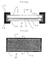
- a general conventional CIS based thin-film solar cell module 1A has a structure obtained by fitting an aluminum frame 5 through a sealing material 6 to peripheral edge parts of an assembly obtained by bonding (attaching) a cover glass 4 through a filling material 8 to a CIS based thin-film solar cell submodule 3 (composed of devices 2 each shown in Fig. 2 which have been electrically connected by patterning) formed on a glass substrate 2A.
- electrodes 3A have been disposed on the periphery of the solar cell submodule 3 surrounded by the aluminum frame 5.
- the aluminum frame 5 and the electrodes 3A and solar cell submodule 3, which are located inside the frame 5, are recognized.
- the aluminum frame 5 has been colored in the same tint (blackish brown) as the solar cell submodule 3, the electrodes 3A has a silver-white color. Because of this, the electrode 3A parts only have a different color. There has hence been a problem that the module as a whole has an uneven color and this impairs the appearance of the solar cell module 1A as shown in Fig. 3 (b) .
- protrudent parts are formed on a surface of a colorless and transparent float glass (white flat glass) by the screen printing of a ceramic ink to thereby cause irregular light reflection and increase the quantity of light received (see, for example, patent document 1).
- these protrudent parts 4 formed from a ceramic ink on the glass surface are not intended to hide the electrode parts to impart a beautiful appearance.
- Known black ceramic materials are ones obtained by compounding zirconia or alumina as a main ingredient with 5-20% by weight one or more coloring materials selected from manganese dioxide, triiron tetroxide, cobalt oxide, nickel oxide, and chromium oxide and burning the composition (see, for example, patent document 2).
- a technique may be usable in which the silver-white electrode 3A parts are hidden by coating with a black coating material, Magic Ink, or the like or applying a black resin (PVC) tape or the like to thereby cause the whole CIS based thin-film solar cell module 1A to have an even color throughout and hence have an improved appearance.
- this technique has a drawback that the steps for solar cell production additionally necessitate such a step and become complicated, leading to an increase in production cost.
- An object of the invention is to hide electrode parts of a solar cell module, which differ in color from other parts of the module, without increasing the number of module assembly/production steps and thereby enable the whole CIS based thin-film solar cell module to have an even color throughout and hence have an improved appearance.
- Another object is to enable the front side and back side of a cover glass 4 to be easily distinguished from each other without fail in a cover glass disposition operation.
- the invention provides a black-ceramic-decorated solar cell module which is a solar cell module having a structure constituted of: a CIS based thin-film solar cell submodule including a glass substrate and, disposed on the glass substrate, CIS based thin-film solar cell device parts which each include superposed layers constituted of a metallic back electrode layer, a CIS based light absorption layer, a buffer layer, and a window layer in this order and which have been electrically connected to each other with a conductive pattern; a tempered cover glass disposed over the upper side of the solar cell submodule; and a back sheet disposed on the back side of the glass substrate through a filling material, wherein the cover glass has a black ceramic layer which has almost the same color as the solar cell submodule and is located in a peripheral edge part on at least one side of the cover glass and over a silver-white electrode part formed in a peripheral area of the solar cell submodule to thereby hide the electrode part.
- the invention provides the black-ceramic-decorated solar cell module, wherein the black ceramic layer has been formed in a peripheral edge part on that side of the cover glass which is in contact with the electrode part of the solar cell submodule.
- the invention provides the black-ceramic-decorated solar cell module, wherein the black ceramic layer is one formed by screen-printing an ink prepared by mixing a glass ingredient and a pigment ingredient with a solvent and baking the ink applied.
- the invention provides the black-ceramic-decorated solar cell module, wherein the glass ingredient for the black ceramic layer includes at least either of bismuth oxide and diboron trioxide and further includes silica (SiO 2 ) or the like, the pigment ingredient includes at least either of manganese dioxide and chromium oxide, and the solvent includes a terpene solvent.
- the glass ingredient for the black ceramic layer includes at least either of bismuth oxide and diboron trioxide and further includes silica (SiO 2 ) or the like
- the pigment ingredient includes at least either of manganese dioxide and chromium oxide
- the solvent includes a terpene solvent.
- the invention provides the black-ceramic-decorated solar cell module according to any one of (1) to (4) above, wherein the baking for forming the black ceramic layer is conducted by utilizing the heating performed when the tempered cover glass is produced through tempering by a heat treatment.
- electrode parts of a solar cell module which differ in color from other parts of the module, can be hidden without increasing the number of module assembly/production steps to thereby enable the whole CIS based thin-film solar cell module to have an even color throughout and hence have an improved appearance.
- the front side and back side of a cover glass 4 can be easily distinguished from each other without fail in a cover glass disposition operation.
- the solar cell module of the invention is a black-ceramic-decorated solar cell module having a beautiful appearance in which the CIS based thin-film solar cell submodule has the same color as the electrode parts of the submodule.
- the electrode parts formed in peripheral areas of the CIS based thin-film solar cell submodule have a silver-white color, which differs from the black color of the power generation part of the submodule.
- the black-ceramic-decorated solar cell module 1 of the invention has a basic constitution including: a CIS based thin-film solar cell submodule 3 composed of CIS based thin-film solar cell devices 2 (see Fig. 2 ) electrically connected by patterning; a cover glass 4 bonded to the submodule 3 through a thermally crosslinked EVA resin film (not shown) as an adhesive; and an aluminum frame 5 attached to the periphery of the submodule/cover glass assembly through a sealing material 6.
- This module 1 may have a structure which includes a back sheet bonded to the back side of the glass substrate 2A through a thermally crosslinked EVA resin film (not shown).
- the CIS based thin-film solar cell devices 2 each have a basic structure such as that shown in Fig. 2 .
- Each device 2 is a pn heterojunction device having a substrate structure composed of high-quality thin-film layers including an alkali barrier layer 2B (which may be omitted), metallic back electrode layer (generally molybdenum) 2C, p-type CIS light absorption layer 2D, high-resistance buffer layer 2E, and n-type window layer (transparent conductive film) 2F which have been superposed in this order on a glass substrate 2A constituted of a blue flat glass or the like.
- an alkali barrier layer 2B which may be omitted
- metallic back electrode layer generally molybdenum
- p-type CIS light absorption layer 2D p-type CIS light absorption layer 2D
- high-resistance buffer layer 2E high-resistance buffer layer
- n-type window layer transparent conductive film
- the light absorption layer 2D is made of a p-type semiconductor such as a thin multinary-compound semiconductor film, in particular, a I-III-VI 2 Group chalcopyrite semiconductor, e.g., copper indium diselenide (CuInSe 2 ), copper indium gallium diselenide (CuInGaSe 2 ), copper gallium diselenide (CuGaSe 2 ), copper indium gallium diselenide-sulfide (Cu(InGa)(SSe) 2 ), copper indium disulfide (CuInS 2 ), copper gallium disulfide (CuGaS 2 ), copper indium gallium disulfide (CuInGaS 2 ), or copper indium gallium diselenide (CuInGaSe 2 ) having a thin film of copper indium gallium diselenide-sulfide (Cu(InGa)(SSe) 2 ) as a surface layer.
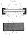
- the black-ceramic-decorated solar cell module 1 of the invention is a solar cell module having a beautiful appearance in which the CIS based thin-film solar cell submodule 3 has the same color as the electrode parts 3A of the submodule, as shown in Fig. 1 .
- the solar cell module 1 has a structure including: a CIS based thin-film solar cell submodule 3 composed of a glass substrate and, disposed thereon, CIS based thin-film solar cell device parts (see Fig.
- a black ceramic layer 7 having almost the same color as the solar cell submodule is formed in those peripheral edge parts of the back side (lower side) of the cover glass 4 which come into contact with the electrode parts of the solar cell submodule.
- the silver-white electrode parts 3A formed in peripheral areas of the solar cell submodule 3 are hidden by the black ceramic layer 7.
- the whole module 1 hence has an even color throughout and has an improved appearance.
- electrode parts 3A have been disposed along the longer sides only of the periphery of the solar cell submodule 3 and, hence, the black ceramic layer 7 also has been formed along the longer sides of the solar cell submodule 3 so as to hide the electrode parts 3A.
- the black ceramic layer 7 it is necessary to form the black ceramic layer 7 in suitable areas according to the positions of the electrode parts 3A. For example, when the electrode parts 3A have been disposed along the shorter sides of the periphery of the solar cell submodule 3, then the black ceramic layer 7 also is formed along the shorter sides of the periphery of the solar cell submodule 3 so as to hide these electrode parts.
- the black ceramic layer 7 may be one formed by screen-printing an ink prepared by mixing a glass ingredient and a pigment ingredient with a solvent and then baking the ink applied.
- the glass ingredient for the black ceramic layer 7 may include at least either of bismuth oxide and diboron trioxide and further include silica (SiO 2 ) or the like.
- the pigment ingredient may include at least either of manganese dioxide and chromium oxide.
- the solvent may include a terpene solvent.
- a baking operation for forming the black ceramic layer 7 in peripheral edge parts of the back side (lower side) of the cover glass 4 may be accomplished by conducting a heat treatment simultaneously with the tempering by a heat treatment to be performed in producing the cover glass 4. Consequently, the formation of the black ceramic layer 7 in this manner does not increase the number of solar cell module assembly/production steps.
- the cover glass 4 has front and back sides, and the back side has a rough surface.
- the black ceramic layer 7 By forming the black ceramic layer 7 on the back side beforehand, the front side and back side of the cover glass 4 can be easily distinguished from each other without fail in an operation for disposing the cover glass 4. Thus, operation efficiency is improved, and the rate of occurrence of defective products can be reduced.
Abstract
Description
- The present invention relates to a black-ceramic-decorated solar cell module which includes a cover glass having a black ceramic layer formed in a peripheral edge part of the back side of the cover glass.
- As shown in
Fig. 3 , a general conventional CIS based thin-filmsolar cell module 1A has a structure obtained by fitting analuminum frame 5 through a sealingmaterial 6 to peripheral edge parts of an assembly obtained by bonding (attaching) a cover glass 4 through afilling material 8 to a CIS based thin-film solar cell submodule 3 (composed ofdevices 2 each shown inFig. 2 which have been electrically connected by patterning) formed on a glass substrate 2A. As shown inFig. 3 (a) and (b) , electrodes 3A have been disposed on the periphery of thesolar cell submodule 3 surrounded by thealuminum frame 5. When the CIS based thin-filmsolar cell module 1A having such a structure is viewed, then thealuminum frame 5 and the electrodes 3A andsolar cell submodule 3, which are located inside theframe 5, are recognized. Although thealuminum frame 5 has been colored in the same tint (blackish brown) as thesolar cell submodule 3, the electrodes 3A has a silver-white color. Because of this, the electrode 3A parts only have a different color. There has hence been a problem that the module as a whole has an uneven color and this impairs the appearance of thesolar cell module 1A as shown inFig. 3 (b) . - With regard to solar cells, there is a technique in which protrudent parts are formed on a surface of a colorless and transparent float glass (white flat glass) by the screen printing of a ceramic ink to thereby cause irregular light reflection and increase the quantity of light received (see, for example, patent document 1). However, these protrudent parts 4 formed from a ceramic ink on the glass surface are not intended to hide the electrode parts to impart a beautiful appearance.
- Known black ceramic materials are ones obtained by compounding zirconia or alumina as a main ingredient with 5-20% by weight one or more coloring materials selected from manganese dioxide, triiron tetroxide, cobalt oxide, nickel oxide, and chromium oxide and burning the composition (see, for example, patent document 2).
- As described above, there has been no idea concerning such a conventional CIS based thin-film
solar cell module 1A that the silver-white electrode 3A parts are hidden to cause the whole CIS based thin-filmsolar cell module 1A to have an even color throughout and hence have an improved appearance. - A technique may be usable in which the silver-white electrode 3A parts are hidden by coating with a black coating material, Magic Ink, or the like or applying a black resin (PVC) tape or the like to thereby cause the whole CIS based thin-film
solar cell module 1A to have an even color throughout and hence have an improved appearance. However, this technique has a drawback that the steps for solar cell production additionally necessitate such a step and become complicated, leading to an increase in production cost. -
- Patent Document 1:
JP-A-2001-298202 - Patent Document 2:
JP-A-7-56070 - The invention eliminates the problem described above. An object of the invention is to hide electrode parts of a solar cell module, which differ in color from other parts of the module, without increasing the number of module assembly/production steps and thereby enable the whole CIS based thin-film solar cell module to have an even color throughout and hence have an improved appearance. Another object is to enable the front side and back side of a cover glass 4 to be easily distinguished from each other without fail in a cover glass disposition operation.
- (1) The invention provides a black-ceramic-decorated solar cell module which is a solar cell module having a structure constituted of: a CIS based thin-film solar cell submodule including a glass substrate and, disposed on the glass substrate, CIS based thin-film solar cell device parts which each include superposed layers constituted of a metallic back electrode layer, a CIS based light absorption layer, a buffer layer, and a window layer in this order and which have been electrically connected to each other with a conductive pattern; a tempered cover glass disposed over the upper side of the solar cell submodule; and a back sheet disposed on the back side of the glass substrate through a filling material,
wherein the cover glass has a black ceramic layer which has almost the same color as the solar cell submodule and is located in a peripheral edge part on at least one side of the cover glass and over a silver-white electrode part formed in a peripheral area of the solar cell submodule to thereby hide the electrode part. - (2) The invention provides the black-ceramic-decorated solar cell module, wherein the black ceramic layer has been formed in a peripheral edge part on that side of the cover glass which is in contact with the electrode part of the solar cell submodule.
- (3) The invention provides the black-ceramic-decorated solar cell module, wherein the black ceramic layer is one formed by screen-printing an ink prepared by mixing a glass ingredient and a pigment ingredient with a solvent and baking the ink applied.
- (4) The invention provides the black-ceramic-decorated solar cell module, wherein the glass ingredient for the black ceramic layer includes at least either of bismuth oxide and diboron trioxide and further includes silica (SiO2) or the like, the pigment ingredient includes at least either of manganese dioxide and chromium oxide, and the solvent includes a terpene solvent.
- (5) The invention provides the black-ceramic-decorated solar cell module according to any one of (1) to (4) above, wherein the baking for forming the black ceramic layer is conducted by utilizing the heating performed when the tempered cover glass is produced through tempering by a heat treatment.
- According to the invention, electrode parts of a solar cell module, which differ in color from other parts of the module, can be hidden without increasing the number of module assembly/production steps to thereby enable the whole CIS based thin-film solar cell module to have an even color throughout and hence have an improved appearance. In addition, the front side and back side of a cover glass 4 can be easily distinguished from each other without fail in a cover glass disposition operation.
-
- [
Fig. 1] Fig. 1 (a) is a view illustrating the constitution of a black-ceramic-decorated solar cell module 1 (CIS based thin-film solar cell module) according to the invention (sectional view; view showing a section formed by cutting along X-X in the plan view (b)).Fig. 1 (b) is a view (plan view) illustrating the constitution of the black-ceramic-decorated solar cell module. - [
Fig. 2] Fig. 2 is a view (sectional view) illustrating the constitution of a CIS based thin-film solar cell device which is part of the components of a black-ceramic-decorated solar cell module according to the invention. - [
Fig. 3] Fig. 3 (a) is a view illustrating the constitution of a conventional CIS based thin-film solar cell module (sectional view; view showing a section formed by cutting along X-X in the plan view (b)).Fig. 3 (b) is a view (plan view) illustrating the constitution of the conventional CIS based thin-film solar cell module. -
- 1 black-ceramic-decorated solar cell module (CIS based thin-film solar cell module) according to the invention
- 1A conventional CIS based thin-film solar cell module
- 2 CIS based thin-film solar cell device
- 2A glass substrate
- 2B alkali barrier layer
- 2C metallic back electrode layer
- 2D p-type CIS light absorption layer
- 2E high-resistance buffer layer
- 2F n-type window layer (transparent conductive film)
- 3 CIS based thin-film solar cell submodule
- 3A electrode part
- 4 cover glass
- 5 aluminum frame
- 6 sealing material
- 7 black ceramic layer
- Embodiments of the invention are explained below. The solar cell module of the invention is a black-ceramic-decorated solar cell module having a beautiful appearance in which the CIS based thin-film solar cell submodule has the same color as the electrode parts of the submodule. The electrode parts formed in peripheral areas of the CIS based thin-film solar cell submodule have a silver-white color, which differs from the black color of the power generation part of the submodule. There has hence been a problem that the module as a whole does not have an even color throughout and module installation results in an impaired appearance.
- As shown in
Fig. 1 , the black-ceramic-decoratedsolar cell module 1 of the invention has a basic constitution including: a CIS based thin-filmsolar cell submodule 3 composed of CIS based thin-film solar cell devices 2 (seeFig. 2 ) electrically connected by patterning; a cover glass 4 bonded to thesubmodule 3 through a thermally crosslinked EVA resin film (not shown) as an adhesive; and analuminum frame 5 attached to the periphery of the submodule/cover glass assembly through a sealingmaterial 6. Thismodule 1 may have a structure which includes a back sheet bonded to the back side of the glass substrate 2A through a thermally crosslinked EVA resin film (not shown). - The CIS based thin-film
solar cell devices 2 each have a basic structure such as that shown inFig. 2 . Eachdevice 2 is a pn heterojunction device having a substrate structure composed of high-quality thin-film layers including an alkali barrier layer 2B (which may be omitted), metallic back electrode layer (generally molybdenum) 2C, p-type CIS light absorption layer 2D, high-resistance buffer layer 2E, and n-type window layer (transparent conductive film) 2F which have been superposed in this order on a glass substrate 2A constituted of a blue flat glass or the like. The light absorption layer 2D is made of a p-type semiconductor such as a thin multinary-compound semiconductor film, in particular, a I-III-VI2 Group chalcopyrite semiconductor, e.g., copper indium diselenide (CuInSe2), copper indium gallium diselenide (CuInGaSe2), copper gallium diselenide (CuGaSe2), copper indium gallium diselenide-sulfide (Cu(InGa)(SSe)2), copper indium disulfide (CuInS2), copper gallium disulfide (CuGaS2), copper indium gallium disulfide (CuInGaS2), or copper indium gallium diselenide (CuInGaSe2) having a thin film of copper indium gallium diselenide-sulfide (Cu(InGa)(SSe)2) as a surface layer. - The black-ceramic-decorated
solar cell module 1 of the invention is a solar cell module having a beautiful appearance in which the CIS based thin-filmsolar cell submodule 3 has the same color as the electrode parts 3A of the submodule, as shown inFig. 1 . Thesolar cell module 1 has a structure including: a CIS based thin-filmsolar cell submodule 3 composed of a glass substrate and, disposed thereon, CIS based thin-film solar cell device parts (seeFig. 2 ) which each include superposed layers constituted of an alkali barrier layer (which may be omitted), a metallic back electrode layer, a CIS based light absorption layer, a buffer layer, and a window layer in this order and which have been electrically connected to each other with a conductive pattern; and a tempered cover glass 4 disposed over the upper side of thesubmodule 3. A blackceramic layer 7 having almost the same color as the solar cell submodule is formed in those peripheral edge parts of the back side (lower side) of the cover glass 4 which come into contact with the electrode parts of the solar cell submodule. As a result, the silver-white electrode parts 3A formed in peripheral areas of thesolar cell submodule 3 are hidden by the blackceramic layer 7. Thewhole module 1 hence has an even color throughout and has an improved appearance. In the module shown inFig. 1 (b) , electrode parts 3A have been disposed along the longer sides only of the periphery of thesolar cell submodule 3 and, hence, the blackceramic layer 7 also has been formed along the longer sides of thesolar cell submodule 3 so as to hide the electrode parts 3A. However, it is necessary to form the blackceramic layer 7 in suitable areas according to the positions of the electrode parts 3A. For example, when the electrode parts 3A have been disposed along the shorter sides of the periphery of thesolar cell submodule 3, then the blackceramic layer 7 also is formed along the shorter sides of the periphery of thesolar cell submodule 3 so as to hide these electrode parts.
Incidentally, even when the blackceramic layer 7 is formed on the front side (upper side) of the cover glass 4, the effect of imparting an even color is obtained. In this case, however, incident light is partly blocked by the blackceramic layer 7 to cast a shadow on thesolar cell submodule 3, resulting in a possibility that the power output of the solar cell might decrease. - The black
ceramic layer 7 may be one formed by screen-printing an ink prepared by mixing a glass ingredient and a pigment ingredient with a solvent and then baking the ink applied. The glass ingredient for the blackceramic layer 7 may include at least either of bismuth oxide and diboron trioxide and further include silica (SiO2) or the like. The pigment ingredient may include at least either of manganese dioxide and chromium oxide. The solvent may include a terpene solvent. - A baking operation for forming the black
ceramic layer 7 in peripheral edge parts of the back side (lower side) of the cover glass 4 may be accomplished by conducting a heat treatment simultaneously with the tempering by a heat treatment to be performed in producing the cover glass 4. Consequently, the formation of the blackceramic layer 7 in this manner does not increase the number of solar cell module assembly/production steps. - The cover glass 4 has front and back sides, and the back side has a rough surface. By forming the black
ceramic layer 7 on the back side beforehand, the front side and back side of the cover glass 4 can be easily distinguished from each other without fail in an operation for disposing the cover glass 4. Thus, operation efficiency is improved, and the rate of occurrence of defective products can be reduced.
Claims (5)
- A black-ceramic-decorated solar cell module which is a solar cell module comprising a structure constituted of: a CIS based thin-film solar cell submodule comprising a glass substrate and, disposed on the glass substrate, CIS based thin-film solar cell device parts which each comprises superposed layers constituted of a metallic back electrode layer, a CIS based light absorption layer, a buffer layer, and a window layer in this order and which have been electrically connected to each other with a conductive pattern; a tempered cover glass disposed over the upper side of the solar cell submodule; and a back sheet disposed on the back side of the glass substrate through a filling material,
wherein the cover glass has a black ceramic layer which has almost the same color as the solar cell submodule and is located in a peripheral edge part on at least one side of the cover glass and over a silver-white electrode part formed in a peripheral area of the solar cell submodule to thereby hide the electrode part. - The black-ceramic-decorated solar cell module according to claim 1, wherein the black ceramic layer has been formed in a peripheral edge part on that side of the cover glass which is in contact with the electrode part of the solar cell submodule.
- The black-ceramic-decorated solar cell module according to claim 1 or 2, wherein the black ceramic layer is one formed by screen-printing an ink prepared by mixing a glass ingredient and a pigment ingredient with a solvent and baking the ink applied.
- The black-ceramic-decorated solar cell module according to claim 3, wherein the glass ingredient for the black ceramic layer comprises at least either of bismuth oxide and diboron trioxide, and silica (SiO2) or the like, the pigment ingredient comprises at least either of manganese dioxide and chromium oxide, and the solvent comprises a terpene solvent.
- The black-ceramic-decorated solar cell module according to any one of claims 1 to 4, wherein the baking for forming the black ceramic layer is conducted by utilizing the heating performed when the tempered cover glass is produced through tempering by a heat treatment.
Applications Claiming Priority (2)
| Application Number | Priority Date | Filing Date | Title |
|---|---|---|---|
| JP2006264259A JP4116658B2 (en) | 2006-09-28 | 2006-09-28 | CIS type thin film solar cell module manufacturing method |
| PCT/JP2007/068702 WO2008038673A1 (en) | 2006-09-28 | 2007-09-26 | Black ceramic decorated solar battery module |
Publications (2)
| Publication Number | Publication Date |
|---|---|
| EP2086017A1 true EP2086017A1 (en) | 2009-08-05 |
| EP2086017A4 EP2086017A4 (en) | 2015-04-22 |
Family
ID=39230109
Family Applications (1)
| Application Number | Title | Priority Date | Filing Date |
|---|---|---|---|
| EP07828448.6A Withdrawn EP2086017A4 (en) | 2006-09-28 | 2007-09-26 | Black ceramic decorated solar battery module |
Country Status (5)
| Country | Link |
|---|---|
| US (1) | US20100037945A1 (en) |
| EP (1) | EP2086017A4 (en) |
| JP (1) | JP4116658B2 (en) |
| TW (1) | TW200816506A (en) |
| WO (1) | WO2008038673A1 (en) |
Cited By (1)
| Publication number | Priority date | Publication date | Assignee | Title |
|---|---|---|---|---|
| CN107706255A (en) * | 2017-09-25 | 2018-02-16 | 宁夏银星能源光伏发电设备制造有限公司 | A kind of transparent photovoltaic modular construction |
Families Citing this family (15)
| Publication number | Priority date | Publication date | Assignee | Title |
|---|---|---|---|---|
| KR101180234B1 (en) * | 2009-04-03 | 2012-09-05 | (주)엘지하우시스 | Building integrated photovoltaic module with design layer |
| US20110146669A1 (en) * | 2009-12-23 | 2011-06-23 | Orion Energy Systems, Inc. | Solar thermal panel |
| US20110155245A1 (en) * | 2009-12-31 | 2011-06-30 | Du Pont Apollo Limited | Solar module having a side insulating member |
| JP5370863B2 (en) * | 2010-07-28 | 2013-12-18 | 株式会社日野樹脂 | Printing method of multifunctional graphic solar cell |
| CN102403396A (en) * | 2010-09-10 | 2012-04-04 | 杜邦太阳能有限公司 | Manufacturing method of thin film solar cell |
| WO2012058454A1 (en) * | 2010-10-29 | 2012-05-03 | First Solar, Inc. | Photovoltaic module substrate |
| TWM426878U (en) | 2011-11-25 | 2012-04-11 | Hulk Energy Technology Co Ltd | Frame structure of solar energy module |
| KR101327099B1 (en) * | 2011-11-29 | 2013-11-07 | 엘지이노텍 주식회사 | Solar cell module and method of fabricating the same |
| JP6619139B2 (en) * | 2014-12-26 | 2019-12-11 | 株式会社マテリアル・コンセプト | Protective glass for solar cell and method for producing the same |
| JP6161046B2 (en) * | 2015-03-16 | 2017-07-12 | 株式会社豊田自動織機 | solar panel |
| JP6867794B6 (en) * | 2016-12-16 | 2021-06-23 | ソーラーフロンティア株式会社 | Photoelectric conversion module |
| JP6484260B2 (en) * | 2017-01-13 | 2019-03-13 | 株式会社豊田自動織機 | Solar cell module and manufacturing method thereof |
| TWI661668B (en) * | 2017-07-25 | 2019-06-01 | 海力雅集成股份有限公司 | Solar module |
| EP3599649B1 (en) * | 2018-07-27 | 2021-10-06 | (CNBM) Bengbu Design & Research Institute for Glass Industry Co., Ltd. | Solar module with structured cover plate and optical interference layer |
| CN110183116B (en) * | 2019-04-28 | 2021-12-24 | 中建材(合肥)新能源有限公司 | Production process of cover plate glass special for solar thin-film battery |
Citations (3)
| Publication number | Priority date | Publication date | Assignee | Title |
|---|---|---|---|---|
| JPH07297433A (en) * | 1994-04-21 | 1995-11-10 | Canon Inc | Solar battery module |
| GB2352998A (en) * | 1999-08-05 | 2001-02-14 | Pilkington Plc | Laminated window |
| EP1331089A1 (en) * | 2002-01-25 | 2003-07-30 | Nippon Sheet Glass Co., Ltd. | Laminated glass sheet for windshield |
Family Cites Families (10)
| Publication number | Priority date | Publication date | Assignee | Title |
|---|---|---|---|---|
| US4321417A (en) * | 1978-06-30 | 1982-03-23 | Exxon Research & Engineering Co. | Solar cell modules |
| JPH02139154U (en) * | 1989-04-24 | 1990-11-20 | ||
| JP3913306B2 (en) * | 1997-01-21 | 2007-05-09 | キヤノン株式会社 | Solar cell module |
| JP2000299486A (en) * | 1999-04-12 | 2000-10-24 | Honda Motor Co Ltd | Solar battery |
| JP2002012445A (en) * | 2000-01-18 | 2002-01-15 | Central Glass Co Ltd | Low fusing point glass |
| FR2810029B1 (en) * | 2000-06-09 | 2003-09-19 | Saint Gobain Vitrage | WATER BASED BLACK ENAMEL COMPOSITION FOR GLASS SUBSTRATE |
| JP2003110127A (en) * | 2001-09-28 | 2003-04-11 | Kyocera Corp | Lighting solar cell module |
| JP4110515B2 (en) * | 2002-04-18 | 2008-07-02 | 本田技研工業株式会社 | Thin film solar cell and manufacturing method thereof |
| JP4271433B2 (en) * | 2002-12-05 | 2009-06-03 | 昭和シェル石油株式会社 | CIS-based thin film solar cell module component recovery method |
| JP2005079170A (en) * | 2003-08-28 | 2005-03-24 | Kyocera Corp | Solar cell module and its manufacturing method |
-
2006
- 2006-09-28 JP JP2006264259A patent/JP4116658B2/en not_active Expired - Fee Related
-
2007
- 2007-09-26 EP EP07828448.6A patent/EP2086017A4/en not_active Withdrawn
- 2007-09-26 US US12/443,388 patent/US20100037945A1/en not_active Abandoned
- 2007-09-26 WO PCT/JP2007/068702 patent/WO2008038673A1/en active Application Filing
- 2007-09-28 TW TW096136153A patent/TW200816506A/en unknown
Patent Citations (3)
| Publication number | Priority date | Publication date | Assignee | Title |
|---|---|---|---|---|
| JPH07297433A (en) * | 1994-04-21 | 1995-11-10 | Canon Inc | Solar battery module |
| GB2352998A (en) * | 1999-08-05 | 2001-02-14 | Pilkington Plc | Laminated window |
| EP1331089A1 (en) * | 2002-01-25 | 2003-07-30 | Nippon Sheet Glass Co., Ltd. | Laminated glass sheet for windshield |
Non-Patent Citations (1)
| Title |
|---|
| See also references of WO2008038673A1 * |
Cited By (2)
| Publication number | Priority date | Publication date | Assignee | Title |
|---|---|---|---|---|
| CN107706255A (en) * | 2017-09-25 | 2018-02-16 | 宁夏银星能源光伏发电设备制造有限公司 | A kind of transparent photovoltaic modular construction |
| CN107706255B (en) * | 2017-09-25 | 2021-03-19 | 宁夏银星能源光伏发电设备制造有限公司 | Transparent photovoltaic module structure |
Also Published As
| Publication number | Publication date |
|---|---|
| EP2086017A4 (en) | 2015-04-22 |
| TW200816506A (en) | 2008-04-01 |
| WO2008038673A1 (en) | 2008-04-03 |
| JP4116658B2 (en) | 2008-07-09 |
| JP2008085128A (en) | 2008-04-10 |
| US20100037945A1 (en) | 2010-02-18 |
Similar Documents
| Publication | Publication Date | Title |
|---|---|---|
| EP2086017A1 (en) | Black ceramic decorated solar battery module | |
| US8859880B2 (en) | Method and structure for tiling industrial thin-film solar devices | |
| CN1219330C (en) | Colored solar cell unit | |
| EP2009702A1 (en) | Cis based thin film solar cell module with pattern display function and its fabrication process | |
| WO2018176527A1 (en) | Solar shingle assembly employing center-converging fingers converging toward electrode | |
| KR101161378B1 (en) | Thin-film type solar cell having white reflective media layer and fabricating method thereof | |
| NL2019318B1 (en) | Photovoltaic module | |
| CN101499492A (en) | Transparent solar cell module | |
| KR20150093291A (en) | Photovoltaic with improved visibility and method for manufacturing thereof | |
| CN111712929B (en) | Solar module with uniform color impression and manufacturing method | |
| EP3522237B1 (en) | Solar cell module | |
| US20150083208A1 (en) | Solar cell and method of fabricating the same | |
| CN115172535B (en) | Preparation method of photovoltaic module and photovoltaic module | |
| CN108321225B (en) | Photovoltaic module and method for producing a photovoltaic module | |
| CN207909894U (en) | It is a kind of that there is the stacked wafer moudle for improving visual effect | |
| NL2019628B1 (en) | Photovoltaic module having scattering patterns | |
| US8049097B2 (en) | Solar cell including cooling channels and method for fabrication | |
| EP2600420A2 (en) | Apparatus for generating electricity using solar power and method for manufacturing same | |
| KR102514859B1 (en) | Media building integrated photo voltaic module | |
| JP4226153B2 (en) | Thin film solar cell dummy module | |
| JP2023010170A (en) | Glass substrate and photoelectric conversion module | |
| CN102094568B (en) | Window for buildings, window for display devices, and multi-functional window structure thereof |
Legal Events
| Date | Code | Title | Description |
|---|---|---|---|
| PUAI | Public reference made under article 153(3) epc to a published international application that has entered the european phase |
Free format text: ORIGINAL CODE: 0009012 |
|
| 17P | Request for examination filed |
Effective date: 20090428 |
|
| AK | Designated contracting states |
Kind code of ref document: A1 Designated state(s): AT BE BG CH CY CZ DE DK EE ES FI FR GB GR HU IE IS IT LI LT LU LV MC MT NL PL PT RO SE SI SK TR |
|
| DAX | Request for extension of the european patent (deleted) | ||
| RAP1 | Party data changed (applicant data changed or rights of an application transferred) |
Owner name: SOLAR FRONTIER K.K. |
|
| RA4 | Supplementary search report drawn up and despatched (corrected) |
Effective date: 20150324 |
|
| RIC1 | Information provided on ipc code assigned before grant |
Ipc: H01L 31/048 20140101ALI20150318BHEP Ipc: H01L 31/02 20060101AFI20150318BHEP |
|
| 17Q | First examination report despatched |
Effective date: 20171220 |
|
| STAA | Information on the status of an ep patent application or granted ep patent |
Free format text: STATUS: THE APPLICATION HAS BEEN WITHDRAWN |
|
| 18W | Application withdrawn |
Effective date: 20180220 |