EP2083486B1 - Elektromagnetische Abschirmung einer Steckeranordnung - Google Patents
Elektromagnetische Abschirmung einer Steckeranordnung Download PDFInfo
- Publication number
- EP2083486B1 EP2083486B1 EP08001349A EP08001349A EP2083486B1 EP 2083486 B1 EP2083486 B1 EP 2083486B1 EP 08001349 A EP08001349 A EP 08001349A EP 08001349 A EP08001349 A EP 08001349A EP 2083486 B1 EP2083486 B1 EP 2083486B1
- Authority
- EP
- European Patent Office
- Prior art keywords
- circuit board
- connector
- electromagnetic shielding
- shielding element
- connector arrangement
- Prior art date
- Legal status (The legal status is an assumption and is not a legal conclusion. Google has not performed a legal analysis and makes no representation as to the accuracy of the status listed.)
- Active
Links
- 230000008878 coupling Effects 0.000 claims description 16
- 238000010168 coupling process Methods 0.000 claims description 16
- 238000005859 coupling reaction Methods 0.000 claims description 16
- 239000004020 conductor Substances 0.000 claims description 13
- 238000000034 method Methods 0.000 claims description 8
- 230000010365 information processing Effects 0.000 claims description 2
- 238000013461 design Methods 0.000 abstract description 2
- 230000003287 optical effect Effects 0.000 description 9
- 230000003071 parasitic effect Effects 0.000 description 9
- 238000005476 soldering Methods 0.000 description 9
- 230000008901 benefit Effects 0.000 description 4
- 238000001914 filtration Methods 0.000 description 4
- 230000005855 radiation Effects 0.000 description 4
- 229910000859 α-Fe Inorganic materials 0.000 description 4
- 230000000694 effects Effects 0.000 description 3
- 238000004519 manufacturing process Methods 0.000 description 3
- 238000001816 cooling Methods 0.000 description 2
- 230000006378 damage Effects 0.000 description 2
- 238000003780 insertion Methods 0.000 description 2
- 230000037431 insertion Effects 0.000 description 2
- 238000006243 chemical reaction Methods 0.000 description 1
- 230000001419 dependent effect Effects 0.000 description 1
- 239000011888 foil Substances 0.000 description 1
- PCHJSUWPFVWCPO-UHFFFAOYSA-N gold Chemical compound [Au] PCHJSUWPFVWCPO-UHFFFAOYSA-N 0.000 description 1
- 239000010931 gold Substances 0.000 description 1
- 229910052737 gold Inorganic materials 0.000 description 1
- 238000010348 incorporation Methods 0.000 description 1
- 238000002955 isolation Methods 0.000 description 1
- 239000000463 material Substances 0.000 description 1
- 239000002184 metal Substances 0.000 description 1
- 229910052751 metal Inorganic materials 0.000 description 1
- 238000012986 modification Methods 0.000 description 1
- 230000004048 modification Effects 0.000 description 1
- 239000012811 non-conductive material Substances 0.000 description 1
- 230000008054 signal transmission Effects 0.000 description 1
- 239000002699 waste material Substances 0.000 description 1
- 239000013585 weight reducing agent Substances 0.000 description 1
Images


Classifications
-
- H—ELECTRICITY
- H01—ELECTRIC ELEMENTS
- H01R—ELECTRICALLY-CONDUCTIVE CONNECTIONS; STRUCTURAL ASSOCIATIONS OF A PLURALITY OF MUTUALLY-INSULATED ELECTRICAL CONNECTING ELEMENTS; COUPLING DEVICES; CURRENT COLLECTORS
- H01R13/00—Details of coupling devices of the kinds covered by groups H01R12/70 or H01R24/00 - H01R33/00
- H01R13/648—Protective earth or shield arrangements on coupling devices, e.g. anti-static shielding
- H01R13/658—High frequency shielding arrangements, e.g. against EMI [Electro-Magnetic Interference] or EMP [Electro-Magnetic Pulse]
- H01R13/6581—Shield structure
- H01R13/6582—Shield structure with resilient means for engaging mating connector
Definitions
- the invention relates to a connector arrangement and a system incorporating the connector arrangement.
- the connector arrangement is equipped with a shielding element for reducing the interference in the area of the connection of the arrangement.
- electromagnetic interference is one of the common problems encountered.
- parasitic radiation is generated from electrical components or circuits during operation which may influence the electrical performance of other electronic components.
- Equally important is a parasitic radiation which frequently occurs at the interface where an electronic device is attached to a high speed network.
- electromagnetic interference may occur between the network cable and the electronic components of, for instance, the circuit board of the electronic device, in both directions.
- EP 1 032 090 A1 relates to a shielded electrical connector system including a conductive chassis fabricated of die-cast metal having an opening, in which an electrical connector is insertable.
- the connector includes a dielectric housing mounting a plurality of terminals.
- a conductive shield is mounted about at least a portion of the housing and includes contact beams projecting outwardly therefrom and applying a normal force to the chassis adjacent to the opening in a direction generally perpendicular to the insertion direction.
- the contact beams are formed to apply a normal force to the surface of the chassis adjacent to the opening therein in a direction parallel to the insertion direction of the connector.
- One object of the invention is to improve the electromagnetic shielding properties of a connector arrangement. Another object is to improve the properties of a connector arrangement so as to meet the high demands on electromagnetic shielding properties for connectors in car applications.
- One aspect of the invention is the utilization of an electromagnetic shielding element in a connector arrangement that together a shielding frame of a connector or alternatively with a device housing (of a device comprising the connector arrangement) is providing an improved electromagnetic shielding of the connector.
- the design of the shielding element and its use in the connector arrangement may provide a Faraday cage in the area of connection between the connector and a circuit board (the so-called mounting area) so that electromagnetic interference of components on the circuit board or from outside the connector arrangement may be significantly reduced.
- the electromagnetic shielding element may be provided as a separate element that can be resiliently and/or detachably engaged to a shielding frame of the connector or the housing of a device housing the connector arrangement.
- the connector arrangement comprises a connector element for receiving a plug or receivable by a socket.
- the connector element is equipped with an electromagnetic shielding frame.
- the connector arrangement comprises a circuit board having a front surface and a rear surface. The connector element is mountable on the front surface of the circuit board, and - when being mounted - covers a certain area of the circuit board, which is referred to as the mounting area.
- the connector arrangement also comprises an electromagnetic shielding element covering at least the rear surface of the circuit board in the circumference of the mounting area of the connector element.
- the electromagnetic shielding element comprises at least one protrusion for resiliently and/or detachably engaging the shielding frame of the connector and for electrically coupling the shielding element to the shielding frame of the connector element.
- the electromagnetic shielding element may also be engaged directly with the housing of a device housing the connector arrangement.
- the device housing is at least partly made out of conductive material, so that a Faraday cage may be provided in the space surrounded by the shielding element and the device housing.
- This alternative connector arrangement is for incorporation in a housing and comprises a connector element for receiving a plug or receivable by a socket and a circuit board having a front surface and a rear surface.
- the connector element can be mounted on the front surface of the circuit board thereby covering a mounting area of the circuit board.
- An electromagnetic shielding element is further provided for covering at least the rear surface of the circuit board in the circumference of the mounting area of the connector element.
- the electromagnetic shielding element comprises at least one protrusion for resiliently and/or detachably engaging the device housing thereby electrically coupling the shielding element to the device housing.
- the electric coupling of the electromagnetic shielding element of the connector arrangement with the at least one protrusion to a shielding frame of the connector element or a device housing is intended to provide a Faraday cage in the mounting area of the connector element on the circuit board.
- the electromagnetic shielding element is provided with plural protrusions for resiliently and/or detachably clipping the electromagnetic shielding element to the connector element and/or the device housing.
- the protrusions are spring clips.
- the circuit board is provided with a plurality of through holes in a circumference of the mounting area of the connector element on the circuit board.
- its protrusions may reach through the through holes for electrically coupling the shielding element to the shielding frame of the connector element or the device housing.
- the protrusions provide a resilient and/or detachable electric coupling of the electromagnetic shielding element to the ground potential of the circuit board.
- the through holes may be for example coated by an electrically conductive material electrically coupled to the ground potential of the circuit board.
- the shielding of the connections between connector and circuit board may be further improved by further using filter elements.
- the circuit board may comprise at least one filter mounted in the circumference of the intersection of the circuit board and an area being formed by at least two of the protrusions of the shielding element.
- the filter element(s) may be for example realized by means of a T-filter or a II-filter.
- the filter has a grounding terminal
- the component housing of the filter is mounted on the circuit board within the mounting area of the connector element, whereby the grounding terminal of the filter is located in the circumference of the before mentioned intersection of the circuit board and an area being formed by at least two of the protrusions of the shielding element.
- the electromagnetic shielding may further comprise a spring clip for resiliently and/or detachably fixing the electromagnetic shielding element to the circuit board.
- the electromagnetic shielding element comprises at least one heat sink for providing a thermal connection between a circuit element on the circuit board, when mounting the connector arrangement. This may for example allow for not only using the electromagnetic shielding element for reducing electromagnetic interference but also for a regulation of the temperature.
- the connector arrangement may be mounted within a housing of a device.
- This housing may be for example conductive so that the shielding frame of the connector element can be electrically coupled to the housing.
- the electromagnetic shielding frame can be for example connected to the ground potential of the housing of the device via the shielding frame of the connector element.
- Another embodiment of the invention relates to a system comprising a connector arrangement according to one the different embodiments described herein, and a second circuit board mounted across to the circuit board of the connector arrangement (referred to as the first circuit board).
- This second circuit board may be further electrically coupled to said circuit board of the connector arrangement (i.e. the fist circuit board).
- the electromagnetic shielding element of this system is electrically coupled to the ground potential of the second circuit board by at least one protrusion of the electromagnetic shielding element.
- the system may for example further comprise at least one filter (element) mounted in the circumference of the intersection of the second circuit board and a fictitious elongation of the part of the shielding element covering at least the rear surface of the circuit board in the circumference of the mounting area of the connector element, which may allow for further improving the shielding of interference.
- at least one filter element mounted in the circumference of the intersection of the second circuit board and a fictitious elongation of the part of the shielding element covering at least the rear surface of the circuit board in the circumference of the mounting area of the connector element, which may allow for further improving the shielding of interference.
- the system may comprise at least one filter (element) mounted on the second circuit board within the circumference of the intersection of the second circuit board and a fictitious elongation of the part of the shielding element that, when the system is mounted, is essentially parallel to the first circuit board.
- the electromagnetic shielding element may be further provided with plural protrusions for resiliently and/or detachably fixing the electromagnetic shielding element to the connector element or the device housing.
- the second circuit board may comprise a plurality of through holes through which, when having mounted the shielding element, at least some of the plurality of protrusions of the electromagnetic shielding element reach through the through holes of the second circuit board for electrically coupling the shielding element to the shielding frame of the connector element or the device housing.
- the protrusions of the second circuit board may provide a resilient and/or detachable electric coupling of the electromagnetic shielding element to the ground potential of the second circuit board.
- the through holes of the second circuit board may be for example coated by an electrically conductive material electrically coupled to the ground potential of the second circuit board.
- Another embodiment of the invention provides a vehicle entertainment and information processing device that is comprising a connector arrangement according to one of the different embodiments described herein or a system according to one of the different embodiments described herein.
- the invention also relates to a method for mounting a connector arrangement comprising a connector element, a circuit board and an electromagnetic shielding element.
- the terminals of the connector element may be connected to the circuit board, to thereby mount the connector element within a mounting area on a front surface of the circuit board, and the electromagnetic shielding element may be further mounted to thereby cover at least the rear surface of the circuit board in the circumference of the mounting area of the connector element.
- At least one protrusion of the shielding element is resiliently and/or detachably engaged to and electrically coupled to the shielding frame of the connector.
- the method comprises connecting terminals of the connector element to the circuit board, to thereby mount the connector element within a mounting area on a front surface of the circuit board, mounting the circuit board and the connector element within the device housing and mounting the electromagnetic shielding element to thereby cover at least the rear surface of the circuit board in the circumference of the mounting area of the connector element, wherein at least one protrusion of the shielding element is resiliently and/or detachably engaged to and electrically coupled to the device housing.
- a second circuit board may be mounted cross to said circuit board, and the electromagnetic shielding element may be and electrically connected to the ground potential of the second circuit board.
- the invention provides a shielding part for a connector element which may be clipped on the sides of the connector element on a conductive frame which is provided around the connector element. Together with the conductive frame, the shielding part forms a Faraday cage so as to electromagnetically shield the certain area of the circuit board which is located underneath the shielding frame respectively shielding element.
- the certain area is also called the mounting area.
- the shielding element may also be clipped directly to the device which comprises the connector arrangement in order to improve the electromagnetic shielding of the connector.
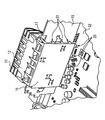
- Fig. 1 illustrates a housing device 18 together with a plurality of circuit boards, a cooling unit and, in particular, a connector arrangement.
- a device may be, for instance, an operating unit of a navigation system in a vehicle or any other multimedia device for being used in an automotive environment.
- the housing may be incorporated in a specific bay of a dashboard of a car.
- the device may be attached to, for instance, a network of a vehicle.
- the network may be an optical or electrical high speed data network for exchanging data between the various devices within the vehicle. It may be a bus system, like a CAN bus or a network with ring topology, like token ring network, for example.
- Such an optical high speed ring network may be for example an optical MOST network.
- each device When devices are operated in a network, necessarily, each device must comprise an interface for connecting to the main network, for instance, of a car. Such an interface is also required for converting any signal between the main network and the device.
- a connector arrangement which comprises a circuit board 13 with a front surface 14 and a rear surface 15 and a connector element 11, which is mounted on the front surface 14 of the circuit board 13.
- the area of the front surface 14, which is covered by the connector element 11 denotes the mounting area of the connector element 11.
- the connector arrangement may also comprise signal converting means for converting the optical signals of the network to electrical signals and vice versa.
- the interface connection may be realized by an optical or electrical plug-and-socket connection.
- An electromagnetic shielding frame 12 may be provided that is typically enclosing a part of the connector element 11. According to one embodiment of the invention, an additional electromagnetic shielding element 16 is provided, which allows to further reduce the electromagnetic interference between the components on the circuit board 32 and the network connector arrangement and vice versa.
- the shielding element 16 may also, for instance, significantly reduce the electromagnetic interference on the electronic components located within the mounting area, caused from outside the connector arrangement and vice versa.
- the shielding element 16 may also, for instance, significantly reduce the electromagnetic interference on the electronic components located within the mounting area, caused from electronic components located outside the mounting area on the circuit board 13 and vice versa.
- electromagnetic shielding element 16 as shown in Fig. 1 , it may also be prevented that electromagnetic interference occurs between the connector element 11 together with the electronic components located on the circuit board within the mounting area and for instance another circuit board or any other electronic element or device inside the device housing 18.
- the electromagnetic shielding element 16 is mounted parallel to the circuit board 13 and covers the mounting area of the rear surface 15 of the circuit board 13. Also shown are protrusions 17 of the electromagnetic shielding element 16, which may be vertical to the surface of the electromagnetic shielding element 16 that covers the mounting area. In one embodiment, the protrusions 17 are in contact with the shielding frame 12 of the connector element 11. Such arrangement of the electromagnetic shielding element 16 being attached to the electromagnetic shielding frame 12 provides a Faraday cage, whereby the mounting area is within the area of the Faraday cage so that electromagnetical isolation is provided.
- the distance between the protrusions may for example be indirectly proportional to the highest parasitic frequency to be filtered.
- the highest parasitic frequency to be filtered is located in the GHZ-range which results in a spacing for the protrusions 17 of the electromagnetic shielding element 16 of approximately 1 cm.
- the electromagnetic shielding element 16 may be either mounted to the electromagnetic shielding frame 12 of the connector element 11 or to the device housing 18 directly. In both cases, a Faraday cage is provided respectively the mounting area of the circuit board 13.
- the protrusions 17 When using the protrusions 17 for mounting the electromagnetic shielding element 16 to the connector element 11, the protrusions provide a resilient and detachable connection to the connector element 1 respectively the electromagnetic shielding frame 12.
- the electromagnetic shielding element 16 may be additionally held and fixed or prevented from slipping by an optional, separate spring clip 20, as shown in Fig. 1 .
- the separate spring clip 20 may be attached to a hole 19 of the circuit board 13 so as to prevent the electromagnetic shielding element 16 from slipping from its position.
- the electromagnetic shielding element 16 may be fixed at the connector element 11, at the electromagnetic shielding frame 12 or at the circuit board 13 by soldering the protrusions thereto.
- Such a conventional fixation by soldering during the manufacturing procedure may however lead to an destruction of the electronic components of the circuit board 13 due to the impact of soldering heat.
- a certain distance between the soldering point and the closest electronic component must be adhered. This may however, lead to an ineffective arrangement of electronic components or to a waste of space on the circuit board 13.
- more electrical components or filter may be placed within the mounting area of the circuit board 13, and the layout of such elements for providing an optimal electromagnetic shielding may be optimized.
- an advantage of using resilient and detachable protrusions 17 is that no soldering has to be carried out for the attachment of the electromagnetic shielding element 16 to the connector element 11 or to the electromagnetic shielding frame 12. Also, by using spring clips 20 for attaching the electromagnetic shielding element 16 to the holes 19 of the circuit board 13, soldering is prevented.
- a further advantage of using resilient and detachable protrusions 17 is that it may be mounted during manufacturing fast and is thus more cost effective compared to conventional ways of mounting such a electromagnetic shielding element 16 to the connector element, i.e. by soldering.
- the spring clip 20 which may be provided on each vertical edge of the electromagnetic shielding element 16 and mounted on a hole 19 on the circuit board 13, it may be ensured that the electromagnetic shielding element 16 also may not slip in the direction of the circuit board 13, which possibly may result in a short circuit on between the electronic components of the mounting area due to the conductive material of the electromagnetic shielding element 16.
- the spring clip 20 may comprise a bent shape so as to ensure a predetermined distance between the electromagnetic shielding element 16 and the circuit board 13.
- the surface of the electromagnetic shielding element 16 may not be plated as shown in Fig. 1 , but rather a lattice.
- the lattice space may be indirectly proportional to the highest parasitic frequency to be filtered, as also valid for the calculation of the distance of the protrusions 17.
- Another possible structure for use as an electromagnetic shielding element may be a conductive punched plate.
- An advantage of the electromagnetic shielding element 16 made of a lattice may be the reduction of material needed for manufacturing which leads to more cost effectiveness. Also, a weight reduction comes along with such an implementation of the electromagnetic shielding element 16 made of a lattice.
- further filter elements may be provided on the circuit board 13, which may be located in the circumference of the intersection of the circuit board 13 and an area being formed by at least two of the protrusions 17 of the electromagnetic shielding element 16.
- the electromagnetic shielding may be further improved.
- a filter may be for instance a T-filter or a II-filter.
- the filter may have a grounding terminal which may be located in the circumference of the intersection of the circuit board 13 and an area being formed by at least two of the protrusions 17 of the electromagnetic shielding element 16.
- the filters further may be provided on both surfaces of the circuit board 13.
- At least one filter may also or alternatively mounted in the circumference of the intersection of the second circuit board 32 and a fictitious elongation of the part of the electromagnetic shielding element 16 covering at least the rear surface 15 of the circuit board 13 in the circumference of the mounting area of the connector element 11.
- the part of the electromagnetic shielding element 16 that covers at least the rear surface 15 of the circuit board 13 may be parallel to the circuit board 13.
- the circuit board 13 may also be denoted as the first circuit board 13, whereby the circuit board 32 may be denoted as the second circuit board 32.
- the surface of the electromagnetic shielding element 16 may be used as a heat sink for dissipating the heat produced by the electronic elements of the mounting area underneath the electromagnetic shielding element 16.
- a cooler may be mounted on the surface of the electromagnetic shielding element 16 to further assist in dissipating the heat.
- a heat sink may also be provided and cooling fins may be supplied as well in order to improve the air convection.
- the holes 19 on the circuit board 13 may be coated with an electrically conductive material (for example gold plated) and may be coupled to the ground potential of the circuit board 13. If the spring clips 20 are soldered to the coated holes 19, the electrical ground potential of the circuit board is also provided to the electromagnetic shielding element 16. Also, any other hole in the circuit board 13 through which the protrusions 17 are mounted may be coated by an electrically conductive material for soldering the protrusions 17 thereto.
- an electrically conductive material for example gold plated
- Fig. 2 shows another, more detailed partial view of a connector arrangement according to one embodiment of the invention and in particular, the mounting of the electromagnetic shielding element 16 to the electromagnetic shielding frame 12 by resiliently and detachably clipping the protrusions 17 of the electromagnetic shielding element 16 to the electromagnetic shielding frame 12.
- the circuit board 13 may comprise through holes 31 through which the protrusions reach to the electromagnetic shielding frame 12.
- the distance between the protrusions may be indirectly proportional to the highest parasitic frequency to be filtered.
- Fig. 3 shows another partial view of the connector arrangement according to one embodiment of the invention, wherein the circuit board 13 has a plurality of through holes 31 in the circumference of the mounting area of the connector element on the circuit board 13.
- the protrusions 17 may reach through the shown through holes 31 so as to electrically couple the electromagnetic shielding element 16 to the shielding frame 12 of the connector element 11.
- Protrusions 33 of the electromagnetic shielding element 16 that may be soldered to the second circuit board 32.
- the distance between each of the protrusions 33 may correlate to that of the protrusions 17 and is also indirectly proportional to the highest parasitic frequency to be filtered.
- protrusions 17 may be realized by spring clips.
- the second circuit 32 board may also comprise through holes through which protrusions may reach so as to electrically couple the electromagnetic shielding element 16 to the electromagnetic shielding frame 12 or device housing 18.
- the through holes of the second circuit board 32 may be coated so as to electrically couple the electromagnetic shielding element 16 to the ground potential of the second circuit board 32 by soldering the protrusions 17 to the coated through holes.
- Fig. 4 shows the front surface 14 of the circuit board 13 and the rear side of the connector element 11 together with the pins for attaching a plug.
- the plug system may be either of electrical or optical nature.
- the plug system may also comprise both, electrical plug connectors and optical ones.
- the upper half of the pin arrangement at the rear side of the connector element 11 may be a plug system for electrically coupling the plug to the socket of the connector element 11, whereby, for example, the lower half may be a plug system for optically coupling the plug to the socket of the connector element 11.
- the electromagnetic shielding frame 12 that comprises conductive nooses, which are slightly bent upwards and which are called resilient springs 41. If the connector element is attached to the device housing 18, the springs 41 get in contact with the conductive material of the device housing 18 and thereby electrically couples the electromagnetic shielding element 16 and the electromagnetic shielding frame 12 to the device housing 18 and thereby to the ground potential of the device housing 18.
- the Faraday cage comprising the electromagnetic shielding element 16, the protrusions 17 and the shielding element 12 is electrically connected to the ground potential of the device housing 18 to ensure a sufficient level of electrical shielding.
- Fig. 5 illustrates another connector arrangement according to a further embodiment of the invention comprising the electromagnetic shielding element 16 together with elongated protrusions 17, being provided on all four sides of the electromagnetic shielding element 16, and that reach from the electromagnetic shielding element 16 to the device housing 18 so as to electrically couple the electromagnetic shielding element 16 to the device housing 18 directly and to form a Faraday cage.
- the electromagnetic shielding frame may not be required to obtain the shielding effect due to a Faraday cage being formed without the shielding frame 12.
- a certain number of protrusions 17 may be elongated as shown in Fig. 5 and reach to the device housing 18 directly, whereby also a certain number of protrusions may be shorter than the ones shown in Fig. 5 and may be coupled to the electromagnetic shielding frame 12.
- the electromagnetic shielding frame 12 together with the short protrusions 17 may form an inner Faraday cage, whereby additionally the elongated protrusions 17 may form an outer Faraday cage. All protrusions 17 may then be electrically coupled to the ground potential of the first circuit board 13, the second circuit board 32 and the device housing 18.
- the electromagnetic shielding element 16 may be provided with protrusion means for ensuring that a certain distance does not fall below a predetermined safety distance between the electromagnetic shielding element 16 and the electronic elements of the mounting area so as to avoid a short circuit due to the conductive material of the electromagnetic shielding element 16.
- protrusion means may be different to the spring clips 20 which are mounted on the edges of the electromagnetic shielding element 16.
- protrusion means may consist of non-conductive material which are fixed on the electromagnetic shielding element 16 and which do not have to be fixed on the circuit board 13.
- the shielding frame 12 may be made of a block out of ferrite, wherein its form determines the filtering properties.
- the ferrite block may further enhance the electromagnetical filtering of the plug connection of the connector arrangement.
- the protrusions 17 of the electromagnetic shielding element 16 reach to the device housing 18, as illustrated in Fig. 5 .
- the shielding element 16 may comprise openings (not shown) through which a flexible conductor foil including a plurality of electrical conductors electrically connecting the circuit board 13 or 32 and a further circuit board with each other can be at least partially led, thereby electromagnetically filtering the plurality of electrical conductors.
- the area surrounding the circumference of the intersection of the circuit boards 32 and 13 may also be provided with a block out of ferrite so as to enhance the electromagnetic shielding of the electrical connection of the circuit boards 13 and 32.
- Fig. 6 illustrates a top view on the connector element 11 together with the electromagnetic shielding element 16 mounted on the electromagnetic shielding frame 12 by using resilient protrusions 17, in particular spring clips.
- the spring clips may be formed in a right angle relative to the electromagnetic shielding element 16 which may be mounted parallel to the surface of the first circuit board 13.
- the figure also shows that the electromagnetic shielding element 16 is electrically coupled to the resilient springs 41 of the electromagnetic shielding frame 12 via the protrusions 17.
- the resilient springs 41 may then be electrically coupled to the device housing 18 upon physically implementing the connector arrangement to the device housing.
- Fig. 7 shows the connector arrangement mechanically implemented in the device housing 18. Also shown are the elongated protrusions 17 which electrically couple the electromagnetic shielding element 16 to the device housing and thereby form a Faraday cage which is coupled to the ground potential of the device housing 18 and provides therewith electromagnetic shielding for the mounting area of the first circuit board 13.
- Fig. 7 further shows a partial view of T-filters mounted on the circuit board 13.
- the filters 72 may be located in the circumference of the intersection of the circuit board 13 and an area being formed by at least two of the protrusions 17 of the electromagnetic shielding element 16.
- the area, which is formed by for instance two protrusions 17 is indicated by the line 71 in Fig. 7 .
- stranded filter elements may be implemented in addition to the T-filters and/or ⁇ -filters on the printed circuit boards 13 or 32. These stranded filter elements may also be implemented instead of T-filters or ⁇ -filters. Thereby, the stranded filter elements may be placed inside the area formed by, for instance, two protrusions 17 as indicated by the line 71 in Fig. 7 . The stranded filter elements further may be placed on the printed circuit board inside or outside the Faraday cage provided in the mounting area of the connector element. If they are provided on the mounting area of the printed circuit board, they may also reach through holes of the shielding element 16 without having electrical contact thereto (not shown).
Claims (25)
- Verbinderanordnung, die umfasst:ein Verbinderelement (11), das einen Stecker aufnehmen kann oder von einer Buchse aufgenommen werden kann, wobei das Verbinderelement einen elektromagnetischen Abschirmrahmen (12) umfasst,eine Leiterplatte (13) mit einer Vorderseite (14) und einer Rückseite (15), wobei das Verbinderelement (11) an der Vorderseite (14) der Leiterplatte (13) angebracht ist und so einen Montagebereich der Leiterplatte (13) abdeckt, undein elektromagnetisches Abschirmelement (16), das wenigstens die Rückseite (15) der Leiterplatte (13) am Umfang des Montagebereiches des Verbinderelementes (11) abdeckt,dadurch gekennzeichnet, dass
das elektromagnetische Abschirmelement (16) eine Vielzahl federnder Vorsprünge (17) zum lösbaren Anklemmen des elektromagnetischen Abschirmelementes (16) an dem Abschirmrahmen (12) des Verbinderelementes (11) sowie zum elektrischen Koppeln des elektromagnetischen Abschirmelementes (16) mit dem elektromagnetischen Abschirmrahmen (12) des Verbinderelementes (11) umfasst. - Verbinderanordnung zum Einsatz in einem Vorrichtungsgehäuse (18), wobei die Verbinderanordnung umfasst:ein Verbinderelement (11), das einen Stecker aufnehmen kann oder von einer Buchse aufgenommen werden kann,eine Leiterplatte (13) mit einer Vorderseite (14) und einer Rückseite (15), wobei das Verbinderelement (11) an der Vorderseite (14) der Leiterplatte (13) angebracht ist und so einen Montagebereich der Leiterplatte (13) abdeckt, undein elektromagnetisches Abschirmelement (16), das wenigstens die Rückseite (15) der Leiterplatte (13) am Umfang des Montagebereiches des Verbinderelementes (11) abdeckt,dadurch gekennzeichnet, dass
das elektromagnetische Abschirmelement (16) eine Vielzahl federnder Vorsprünge (17) umfasst, mit denen das elektromagnetische Abschirmelement (16) an dem Vorrichtungsgehäuse (18) lösbar angeklemmt wird, wodurch das Abschirmelement (16) elektrisch mit dem Vorrichtungsgehäuse (18) verbunden wird. - Verbinderanordnung nach Anspruch 1 oder 2, dadurch gekennzeichnet, dass das elektrische Koppeln des elektromagnetischen Abschirmelementes (16) mit einem Abschirmrahmen (12) des Verbinderelementes (11) oder einem Vorrichtungsgehäuse (18) mittels der Vielzahl von Vorsprüngen (17) einen Faradayschen Käfig in dem Montagebereich des Verbinderelementes (11) an der Leiterplatte (13) bildet.
- Verbinderanordnung nach Anspruch 3, dadurch gekennzeichnet, dass die Vorsprünge (17) Federklemmen sind.
- Verbinderanordnung nach Anspruch 3 oder 4, dadurch gekennzeichnet, dass die Leiterplatte (13) eine Vielzahl von Durchgangslöchern (31) in einem Umfang des Anbringungsbereiches des Verbinderelementes (11) an der Leiterplatte (13) aufweist, wobei, wenn das elektromagnetische Abschirmelement (16) angebracht ist, die Vorsprünge (17) durch die Durchgangslöcher (31) hindurch reichen, um das Abschirmelement (16) elektrisch mit dem Abschirmrahmen (12) des Verbinderelementes (11) oder dem Vorrichtungsgehäuse (18) zu koppeln.
- Verbinderanordnung nach Anspruch 5, dadurch gekennzeichnet, dass die Vorsprünge (17) eine federnde und/oder lösbare elektrische Kopplung des elektromagnetischen Abschirmelementes (16) mit dem Erdpotential der Leiterplatte (13) erzeugen.
- Verbinderanordnung nach Anspruch 6, dadurch gekennzeichnet, dass die Durchgangslöcher (31) mit einem elektrisch leitendem Material beschichtet sind, das elektrisch mit dem Erdpotential der Leiterplatte (13) gekoppelt ist.
- Verbinderanordnung nach einem der Ansprüche 3 bis 7, dadurch gekennzeichnet, dass die Leiterplatte (13) wenigstens ein Filter umfasst, das am Umfang der Überschneidung der Leiterplatte (13) und einer Fläche angebracht ist, die durch wenigstens zwei der Vorsprünge (17) des Abschirmelementes (16) gebildet wird.
- Verbinderanordnung nach Anspruch 8, dadurch gekennzeichnet, dass das wenigstens eine Filterelement ein T-Filter oder ein Π-Filter ist.
- Verbinderanordnung nach Anspruch 8 oder 9, dadurch gekennzeichnet, dass das Filter einen Erdungsanschluss hat, und wobei das Bauteilgehäuse des Filters innerhalb des Montagebereiches des Verbinderelementes (11) an der Leiterplatte (13) angebracht ist und sich der Erdungsanschluss des Filters am Umfang der Überschneidung befindet.
- Verbinderanordnung nach einem der Ansprüche 1 bis 10, dadurch gekennzeichnet, dass die elektromagnetische Abschirmung (16) eine Federklemme zum federnden und/oder lösbaren Fixieren des elektromagnetischen Abschirmelementes (16) an der Leiterplatte (13) umfasst.
- Verbinderanordnung nach einem der Ansprüche 1 bis 11, dadurch gekennzeichnet, dass das elektromagnetische Abschirmelement (16) wenigstens eine Wärmesenke umfasst, die eine thermische Verbindung zwischen einem Schaltungselement an der Leiterplatte (13) beim Anbringen der Verbinderanordnung schafft.
- Verbinderanordnung nach einem der Ansprüche 1 bis 12, dadurch gekennzeichnet, dass die Verbinderanordnung im Inneren eines leitenden Gehäuses angebracht ist, und wobei der Abschirmrahmen (12) des Verbinderelementes (11) elektrisch mit dem Gehäuse gekoppelt ist.
- Verbinderanordnung nach Anspruch 13, dadurch gekennzeichnet, dass der elektromagnetische Abschirmrahmen (12) über den Abschirmrahmen (12) des Verbinderelementes mit dem Erdpotential des Gehäuses des Gerätes verbunden ist.
- System, das eine Verbinderanordnung nach einem der Ansprüche 1 bis 14 sowie eine zweite Leiterplatte (32) umfasst, die quer zu der Leiterplatte (13) der Verbinderanordnung angebracht ist, die eine erste Leiterplatte (13) bildet, und elektrisch mit der Leiterplatte (13) der Verbinderanordnung gekoppelt ist.
- System nach Anspruch 15, dadurch gekennzeichnet, dass das elektromagnetische Abschirmelement (16) durch wenigstens einen Vorsprung (17) des elektromagnetischen Abschirmelementes (16) elektrisch mit dem Erdpotential der zweiten Leiterplatte (32) gekoppelt ist.
- System nach Anspruch 15 oder 16, dadurch gekennzeichnet, dass es des Weiteren wenigstens ein Filter umfasst, das am Umfang der Überschneidung der zweiten Leiterplatte (32) und einer imaginären Verlängerung des Teils des Abschirmelementes (16) angebracht ist, der wenigstens die Rückseite (15) der Leiterplatte (13) am Umfang des Anbringungsbereiches des Verbinderelementes (11) abdeckt.
- System nach einem der Ansprüche 15 bis 17, dadurch gekennzeichnet, dass es des Weiteren wenigstens ein Filter umfasst, das an der zweiten Leiterplatte (32) innerhalb des Umfangs der Überschneidung der zweiten Leiterplatte (32) und einer imaginären Verlängerung des Teils des Abschirmelementes (16) angebracht ist, der, wenn das System angebracht ist, im Wesentlichen parallel zu der ersten Leiterplatte (13) ist.
- System nach einem der Ansprüche 15 bis 18, dadurch gekennzeichnet, dass das elektromagnetische Abschirmelement (16) mit mehreren Vorsprüngen zum federnden und/oder lösbaren Fixieren des elektromagnetischen Abschirmelementes (16) an dem Verbinderelement (11) oder dem Vorrichtungsgehäuse (18) versehen ist, und
wobei die zweite Leiterplatte (32) eine Vielzahl von Durchgangslöchern umfasst, durch die, wenn das System angebracht ist, wenigstens einige der Vielzahl von Vorsprüngen (17) des elektromagnetischen Abschirmelementes (16) hindurchreichen, wobei die Durchgangslöcher der zweiten Leiterplatte (32) dazu dienen, das Abschirmelement (16) elektrisch mit dem Abschirmrahmen (12) des Verbinderelementes (11) oder des Vorrichtungsgehäuses (18) zu koppeln. - System nach Anspruch 19, dadurch gekennzeichnet, dass die Vorsprünge (17) der zweiten Leiterplatte (32) eine federnde und/oder lösbare elektrische Kopplung des elektromagnetischen Abschirmelementes (16) mit dem Erdpotential der zweiten Leiterplatte (32) erzeugen.
- System nach Anspruch 20, dadurch gekennzeichnet, dass die Durchgangslöcher der zweiten Leiterplatte (32) mit einem elektrisch leitendem Material beschichtet sind, das elektrisch mit dem Erdpotential der zweiten Leiterplatte (32) gekoppelt ist.
- Unterhaltungs-und-Informationsverarbeitungs-Vorrichtung für Fahrzeuge, dadurch gekennzeichnet, dass sie eine Verbinderanordnung nach einem der Ansprüche 1 bis 14 oder ein System nach einem der Ansprüche 15 bis 21 umfasst.
- Verfahren zum Anbringen einer Verbinderanordnung, die ein Verbinderelement (11), eine Leiterplatte (13) und ein elektromagnetisches Abschirmelement (16) umfasst, wobei das Verfahren umfasst:Verbinden von Anschlüssen des Verbinderelementes (11) mit der Leiterplatte (13), um so das Verbinderelement (11) innerhalb eines Montagebereiches an einer Vorderseite (14) der Leiterplatte (13) anzubringen, undAnbringen des elektromagnetischen Abschirmelementes (16), um so wenigstens die Rückseite (15) der Leiterplatte (13) am Umfang des Montagebereiches des Verbinderelementes (11) abzudecken,dadurch gekennzeichnet, dass
eine Vielzahl federnder Vorsprünge (17) des elektromagnetischen Abschirmelementes (16) lösbar an dem elektromagnetischen Abschirmrahmen (12) des Verbinderelementes (11) angeklemmt und elektrisch damit gekoppelt sind. - Verfahren zum Anbringen einer Verbinderanordnung, die ein Verbinderelement (11), eine Leiterplatte (13) und ein elektromagnetisches Abschirmelement (16) umfasst, innerhalb eines Vorrichtungsgehäuses (18), wobei das Verfahren umfasst:Verbinden von Anschlüssen des Verbinderelementes (11) mit der Leiterplatte (13), um so das Verbinderelement (11) innerhalb eines Montagebereiches an einer Vorderseite (14) der Leiterplatte (13) anzubringen,Anbringen der Leiterplatte (13) und des Verbinderelementes (11) innerhalb des Vorrichtungsgehäuses (18), undAnbringen des elektromagnetischen Abschirmelementes (16), um so wenigstens die Rückseite (15) der Leiterplatte (13) am Umfang des Montagebereiches des Verbinderelementes (11) abzudecken,dadurch gekennzeichnet, dass
eine Vielzahl federnder Vorsprünge (17) des Abschirmelementes (16) lösbar an dem Vorrichtungsgehäuse (18) angeklemmt und elektrisch damit gekoppelt sind. - Verfahren nach Anspruch 23 oder 24, dadurch gekennzeichnet, dass es des Weiteren die Schritte des Anbringens einer zweiten Leiterplatte (32) quer zu der Leiterplatte (13) und des elektrischen Verbindens des elektromagnetischen Abschirmelementes (16) mit dem Erdpotential der zweiten Leiterplatte (32) umfasst.
Priority Applications (3)
| Application Number | Priority Date | Filing Date | Title |
|---|---|---|---|
| DE602008006345T DE602008006345D1 (de) | 2008-01-24 | 2008-01-24 | Elektromagnetische Abschirmung einer Steckeranordnung |
| EP08001349A EP2083486B1 (de) | 2008-01-24 | 2008-01-24 | Elektromagnetische Abschirmung einer Steckeranordnung |
| AT08001349T ATE506721T1 (de) | 2008-01-24 | 2008-01-24 | Elektromagnetische abschirmung einer steckeranordnung |
Applications Claiming Priority (1)
| Application Number | Priority Date | Filing Date | Title |
|---|---|---|---|
| EP08001349A EP2083486B1 (de) | 2008-01-24 | 2008-01-24 | Elektromagnetische Abschirmung einer Steckeranordnung |
Publications (2)
| Publication Number | Publication Date |
|---|---|
| EP2083486A1 EP2083486A1 (de) | 2009-07-29 |
| EP2083486B1 true EP2083486B1 (de) | 2011-04-20 |
Family
ID=39494892
Family Applications (1)
| Application Number | Title | Priority Date | Filing Date |
|---|---|---|---|
| EP08001349A Active EP2083486B1 (de) | 2008-01-24 | 2008-01-24 | Elektromagnetische Abschirmung einer Steckeranordnung |
Country Status (3)
| Country | Link |
|---|---|
| EP (1) | EP2083486B1 (de) |
| AT (1) | ATE506721T1 (de) |
| DE (1) | DE602008006345D1 (de) |
Family Cites Families (2)
| Publication number | Priority date | Publication date | Assignee | Title |
|---|---|---|---|---|
| US5014160A (en) * | 1989-07-05 | 1991-05-07 | Digital Equipment Corporation | EMI/RFI shielding method and apparatus |
| US6206728B1 (en) | 1999-02-22 | 2001-03-27 | Molex Incorporated | Shielded electrical connector system |
-
2008
- 2008-01-24 EP EP08001349A patent/EP2083486B1/de active Active
- 2008-01-24 DE DE602008006345T patent/DE602008006345D1/de active Active
- 2008-01-24 AT AT08001349T patent/ATE506721T1/de not_active IP Right Cessation
Also Published As
| Publication number | Publication date |
|---|---|
| ATE506721T1 (de) | 2011-05-15 |
| DE602008006345D1 (de) | 2011-06-01 |
| EP2083486A1 (de) | 2009-07-29 |
Similar Documents
| Publication | Publication Date | Title |
|---|---|---|
| JP5109663B2 (ja) | プラガブル光送受信モジュール実装装置 | |
| EP2034554B1 (de) | Leiterplatten-einbauverbinder und einfangvorrichtung | |
| TW201014079A (en) | Electrical connector assembly | |
| US20070197060A1 (en) | Transceiver cage assembly with grounding device | |
| CN101902022B (zh) | 用于车辆的接线盒 | |
| JP4964218B2 (ja) | 光電気変換装置、及び、これに用いる光電気複合型コネクタ | |
| US6380482B1 (en) | Electromagnetic compatibility sleeve for electrical interconnections | |
| US6896553B2 (en) | Electrical connector with an integrated modem | |
| US10170874B1 (en) | Cable assembly having a substrate with multiple passive filtering devices between two sections of the cable assembly | |
| US9039430B2 (en) | Electric connector, train-information transmission/reception system, and method for connecting electric connector | |
| CN110998990B (zh) | 一种具有高屏蔽效率的电磁干扰笼罩和边框夹的收发器插座 | |
| CN213959261U (zh) | 一种屏蔽笼及其电连接器 | |
| EP1725900B1 (de) | Optischer verbinder | |
| TW202127078A (zh) | 電纜連接器以及板連接器 | |
| JP2009146570A (ja) | ジョイントコネクタ | |
| EP2083486B1 (de) | Elektromagnetische Abschirmung einer Steckeranordnung | |
| CN114731007A (zh) | 可拆卸有线前面板连接器 | |
| CN103857267A (zh) | 电子设备的屏蔽结构 | |
| US6077119A (en) | Shielding device for a connector unit and the connector unit using the same | |
| US11710918B2 (en) | Cable receptacle connector for a communication system | |
| EP1527502B1 (de) | Steckverbindersystem zum verbinden eines ersten teils an einem zweiten teil | |
| SE502998C2 (sv) | Elektriskt kopplingsdon samt kretskort | |
| JP2003508936A (ja) | Emi抑制配線プレートを備えた電気部品の組立体及びその製造方法並びにemi抑制配線プレート | |
| JP2005116400A (ja) | 光アクティブコネクタ | |
| EP2651200B1 (de) | Digitales Schutzrelais |
Legal Events
| Date | Code | Title | Description |
|---|---|---|---|
| PUAI | Public reference made under article 153(3) epc to a published international application that has entered the european phase |
Free format text: ORIGINAL CODE: 0009012 |
|
| AK | Designated contracting states |
Kind code of ref document: A1 Designated state(s): AT BE BG CH CY CZ DE DK EE ES FI FR GB GR HR HU IE IS IT LI LT LU LV MC MT NL NO PL PT RO SE SI SK TR |
|
| AX | Request for extension of the european patent |
Extension state: AL BA MK RS |
|
| 17P | Request for examination filed |
Effective date: 20091120 |
|
| AKX | Designation fees paid |
Designated state(s): AT BE BG CH CY CZ DE DK EE ES FI FR GB GR HR HU IE IS IT LI LT LU LV MC MT NL NO PL PT RO SE SI SK TR |
|
| 17Q | First examination report despatched |
Effective date: 20100521 |
|
| GRAP | Despatch of communication of intention to grant a patent |
Free format text: ORIGINAL CODE: EPIDOSNIGR1 |
|
| GRAS | Grant fee paid |
Free format text: ORIGINAL CODE: EPIDOSNIGR3 |
|
| GRAA | (expected) grant |
Free format text: ORIGINAL CODE: 0009210 |
|
| AK | Designated contracting states |
Kind code of ref document: B1 Designated state(s): AT BE BG CH CY CZ DE DK EE ES FI FR GB GR HR HU IE IS IT LI LT LU LV MC MT NL NO PL PT RO SE SI SK TR |
|
| REG | Reference to a national code |
Ref country code: GB Ref legal event code: FG4D |
|
| REG | Reference to a national code |
Ref country code: CH Ref legal event code: EP |
|
| REG | Reference to a national code |
Ref country code: IE Ref legal event code: FG4D |
|
| REF | Corresponds to: |
Ref document number: 602008006345 Country of ref document: DE Date of ref document: 20110601 Kind code of ref document: P |
|
| REG | Reference to a national code |
Ref country code: DE Ref legal event code: R096 Ref document number: 602008006345 Country of ref document: DE Effective date: 20110601 |
|
| REG | Reference to a national code |
Ref country code: NL Ref legal event code: VDEP Effective date: 20110420 |
|
| LTIE | Lt: invalidation of european patent or patent extension |
Effective date: 20110420 |
|
| PG25 | Lapsed in a contracting state [announced via postgrant information from national office to epo] |
Ref country code: SE Free format text: LAPSE BECAUSE OF FAILURE TO SUBMIT A TRANSLATION OF THE DESCRIPTION OR TO PAY THE FEE WITHIN THE PRESCRIBED TIME-LIMIT Effective date: 20110420 Ref country code: PT Free format text: LAPSE BECAUSE OF FAILURE TO SUBMIT A TRANSLATION OF THE DESCRIPTION OR TO PAY THE FEE WITHIN THE PRESCRIBED TIME-LIMIT Effective date: 20110822 Ref country code: NO Free format text: LAPSE BECAUSE OF FAILURE TO SUBMIT A TRANSLATION OF THE DESCRIPTION OR TO PAY THE FEE WITHIN THE PRESCRIBED TIME-LIMIT Effective date: 20110720 Ref country code: LT Free format text: LAPSE BECAUSE OF FAILURE TO SUBMIT A TRANSLATION OF THE DESCRIPTION OR TO PAY THE FEE WITHIN THE PRESCRIBED TIME-LIMIT Effective date: 20110420 Ref country code: HR Free format text: LAPSE BECAUSE OF FAILURE TO SUBMIT A TRANSLATION OF THE DESCRIPTION OR TO PAY THE FEE WITHIN THE PRESCRIBED TIME-LIMIT Effective date: 20110420 |
|
| PG25 | Lapsed in a contracting state [announced via postgrant information from national office to epo] |
Ref country code: LV Free format text: LAPSE BECAUSE OF FAILURE TO SUBMIT A TRANSLATION OF THE DESCRIPTION OR TO PAY THE FEE WITHIN THE PRESCRIBED TIME-LIMIT Effective date: 20110420 Ref country code: IS Free format text: LAPSE BECAUSE OF FAILURE TO SUBMIT A TRANSLATION OF THE DESCRIPTION OR TO PAY THE FEE WITHIN THE PRESCRIBED TIME-LIMIT Effective date: 20110820 Ref country code: AT Free format text: LAPSE BECAUSE OF FAILURE TO SUBMIT A TRANSLATION OF THE DESCRIPTION OR TO PAY THE FEE WITHIN THE PRESCRIBED TIME-LIMIT Effective date: 20110420 Ref country code: FI Free format text: LAPSE BECAUSE OF FAILURE TO SUBMIT A TRANSLATION OF THE DESCRIPTION OR TO PAY THE FEE WITHIN THE PRESCRIBED TIME-LIMIT Effective date: 20110420 Ref country code: BE Free format text: LAPSE BECAUSE OF FAILURE TO SUBMIT A TRANSLATION OF THE DESCRIPTION OR TO PAY THE FEE WITHIN THE PRESCRIBED TIME-LIMIT Effective date: 20110420 Ref country code: SI Free format text: LAPSE BECAUSE OF FAILURE TO SUBMIT A TRANSLATION OF THE DESCRIPTION OR TO PAY THE FEE WITHIN THE PRESCRIBED TIME-LIMIT Effective date: 20110420 Ref country code: GR Free format text: LAPSE BECAUSE OF FAILURE TO SUBMIT A TRANSLATION OF THE DESCRIPTION OR TO PAY THE FEE WITHIN THE PRESCRIBED TIME-LIMIT Effective date: 20110721 Ref country code: ES Free format text: LAPSE BECAUSE OF FAILURE TO SUBMIT A TRANSLATION OF THE DESCRIPTION OR TO PAY THE FEE WITHIN THE PRESCRIBED TIME-LIMIT Effective date: 20110731 Ref country code: CY Free format text: LAPSE BECAUSE OF FAILURE TO SUBMIT A TRANSLATION OF THE DESCRIPTION OR TO PAY THE FEE WITHIN THE PRESCRIBED TIME-LIMIT Effective date: 20110420 |
|
| PG25 | Lapsed in a contracting state [announced via postgrant information from national office to epo] |
Ref country code: NL Free format text: LAPSE BECAUSE OF FAILURE TO SUBMIT A TRANSLATION OF THE DESCRIPTION OR TO PAY THE FEE WITHIN THE PRESCRIBED TIME-LIMIT Effective date: 20110420 |
|
| PG25 | Lapsed in a contracting state [announced via postgrant information from national office to epo] |
Ref country code: EE Free format text: LAPSE BECAUSE OF FAILURE TO SUBMIT A TRANSLATION OF THE DESCRIPTION OR TO PAY THE FEE WITHIN THE PRESCRIBED TIME-LIMIT Effective date: 20110420 Ref country code: CZ Free format text: LAPSE BECAUSE OF FAILURE TO SUBMIT A TRANSLATION OF THE DESCRIPTION OR TO PAY THE FEE WITHIN THE PRESCRIBED TIME-LIMIT Effective date: 20110420 |
|
| PLBE | No opposition filed within time limit |
Free format text: ORIGINAL CODE: 0009261 |
|
| STAA | Information on the status of an ep patent application or granted ep patent |
Free format text: STATUS: NO OPPOSITION FILED WITHIN TIME LIMIT |
|
| PG25 | Lapsed in a contracting state [announced via postgrant information from national office to epo] |
Ref country code: PL Free format text: LAPSE BECAUSE OF FAILURE TO SUBMIT A TRANSLATION OF THE DESCRIPTION OR TO PAY THE FEE WITHIN THE PRESCRIBED TIME-LIMIT Effective date: 20110420 Ref country code: DK Free format text: LAPSE BECAUSE OF FAILURE TO SUBMIT A TRANSLATION OF THE DESCRIPTION OR TO PAY THE FEE WITHIN THE PRESCRIBED TIME-LIMIT Effective date: 20110420 Ref country code: SK Free format text: LAPSE BECAUSE OF FAILURE TO SUBMIT A TRANSLATION OF THE DESCRIPTION OR TO PAY THE FEE WITHIN THE PRESCRIBED TIME-LIMIT Effective date: 20110420 Ref country code: RO Free format text: LAPSE BECAUSE OF FAILURE TO SUBMIT A TRANSLATION OF THE DESCRIPTION OR TO PAY THE FEE WITHIN THE PRESCRIBED TIME-LIMIT Effective date: 20110420 |
|
| 26N | No opposition filed |
Effective date: 20120123 |
|
| REG | Reference to a national code |
Ref country code: DE Ref legal event code: R097 Ref document number: 602008006345 Country of ref document: DE Effective date: 20120123 |
|
| PG25 | Lapsed in a contracting state [announced via postgrant information from national office to epo] |
Ref country code: IT Free format text: LAPSE BECAUSE OF FAILURE TO SUBMIT A TRANSLATION OF THE DESCRIPTION OR TO PAY THE FEE WITHIN THE PRESCRIBED TIME-LIMIT Effective date: 20110420 |
|
| PG25 | Lapsed in a contracting state [announced via postgrant information from national office to epo] |
Ref country code: MC Free format text: LAPSE BECAUSE OF NON-PAYMENT OF DUE FEES Effective date: 20120131 |
|
| REG | Reference to a national code |
Ref country code: CH Ref legal event code: PL |
|
| REG | Reference to a national code |
Ref country code: IE Ref legal event code: MM4A |
|
| PG25 | Lapsed in a contracting state [announced via postgrant information from national office to epo] |
Ref country code: LI Free format text: LAPSE BECAUSE OF NON-PAYMENT OF DUE FEES Effective date: 20120131 Ref country code: CH Free format text: LAPSE BECAUSE OF NON-PAYMENT OF DUE FEES Effective date: 20120131 |
|
| PG25 | Lapsed in a contracting state [announced via postgrant information from national office to epo] |
Ref country code: IE Free format text: LAPSE BECAUSE OF NON-PAYMENT OF DUE FEES Effective date: 20120124 |
|
| PG25 | Lapsed in a contracting state [announced via postgrant information from national office to epo] |
Ref country code: BG Free format text: LAPSE BECAUSE OF FAILURE TO SUBMIT A TRANSLATION OF THE DESCRIPTION OR TO PAY THE FEE WITHIN THE PRESCRIBED TIME-LIMIT Effective date: 20110720 |
|
| PG25 | Lapsed in a contracting state [announced via postgrant information from national office to epo] |
Ref country code: MT Free format text: LAPSE BECAUSE OF FAILURE TO SUBMIT A TRANSLATION OF THE DESCRIPTION OR TO PAY THE FEE WITHIN THE PRESCRIBED TIME-LIMIT Effective date: 20110420 |
|
| PG25 | Lapsed in a contracting state [announced via postgrant information from national office to epo] |
Ref country code: TR Free format text: LAPSE BECAUSE OF FAILURE TO SUBMIT A TRANSLATION OF THE DESCRIPTION OR TO PAY THE FEE WITHIN THE PRESCRIBED TIME-LIMIT Effective date: 20110420 |
|
| PG25 | Lapsed in a contracting state [announced via postgrant information from national office to epo] |
Ref country code: LU Free format text: LAPSE BECAUSE OF NON-PAYMENT OF DUE FEES Effective date: 20120124 |
|
| PG25 | Lapsed in a contracting state [announced via postgrant information from national office to epo] |
Ref country code: HU Free format text: LAPSE BECAUSE OF FAILURE TO SUBMIT A TRANSLATION OF THE DESCRIPTION OR TO PAY THE FEE WITHIN THE PRESCRIBED TIME-LIMIT Effective date: 20080124 |
|
| REG | Reference to a national code |
Ref country code: FR Ref legal event code: PLFP Year of fee payment: 8 |
|
| PGFP | Annual fee paid to national office [announced via postgrant information from national office to epo] |
Ref country code: FR Payment date: 20150119 Year of fee payment: 8 |
|
| REG | Reference to a national code |
Ref country code: FR Ref legal event code: ST Effective date: 20160930 |
|
| PG25 | Lapsed in a contracting state [announced via postgrant information from national office to epo] |
Ref country code: FR Free format text: LAPSE BECAUSE OF NON-PAYMENT OF DUE FEES Effective date: 20160201 |
|
| PGFP | Annual fee paid to national office [announced via postgrant information from national office to epo] |
Ref country code: GB Payment date: 20181219 Year of fee payment: 12 |
|
| GBPC | Gb: european patent ceased through non-payment of renewal fee |
Effective date: 20200124 |
|
| PG25 | Lapsed in a contracting state [announced via postgrant information from national office to epo] |
Ref country code: GB Free format text: LAPSE BECAUSE OF NON-PAYMENT OF DUE FEES Effective date: 20200124 |
|
| REG | Reference to a national code |
Ref country code: DE Ref legal event code: R082 Ref document number: 602008006345 Country of ref document: DE Representative=s name: MAUCHER JENKINS PATENTANWAELTE & RECHTSANWAELT, DE |
|
| P01 | Opt-out of the competence of the unified patent court (upc) registered |
Effective date: 20230526 |
|
| PGFP | Annual fee paid to national office [announced via postgrant information from national office to epo] |
Ref country code: DE Payment date: 20231219 Year of fee payment: 17 |