EP2083262B1 - Resistiver Wasserstoffsensor - Google Patents
Resistiver Wasserstoffsensor Download PDFInfo
- Publication number
- EP2083262B1 EP2083262B1 EP08001491.3A EP08001491A EP2083262B1 EP 2083262 B1 EP2083262 B1 EP 2083262B1 EP 08001491 A EP08001491 A EP 08001491A EP 2083262 B1 EP2083262 B1 EP 2083262B1
- Authority
- EP
- European Patent Office
- Prior art keywords
- layer
- resistance
- hydrogen sensor
- resistance layer
- resistive
- Prior art date
- Legal status (The legal status is an assumption and is not a legal conclusion. Google has not performed a legal analysis and makes no representation as to the accuracy of the status listed.)
- Ceased
Links
Images


Classifications
-
- G—PHYSICS
- G01—MEASURING; TESTING
- G01N—INVESTIGATING OR ANALYSING MATERIALS BY DETERMINING THEIR CHEMICAL OR PHYSICAL PROPERTIES
- G01N27/00—Investigating or analysing materials by the use of electric, electrochemical, or magnetic means
- G01N27/02—Investigating or analysing materials by the use of electric, electrochemical, or magnetic means by investigating impedance
- G01N27/04—Investigating or analysing materials by the use of electric, electrochemical, or magnetic means by investigating impedance by investigating resistance
- G01N27/12—Investigating or analysing materials by the use of electric, electrochemical, or magnetic means by investigating impedance by investigating resistance of a solid body in dependence upon absorption of a fluid; of a solid body in dependence upon reaction with a fluid, for detecting components in the fluid
-
- G—PHYSICS
- G01—MEASURING; TESTING
- G01N—INVESTIGATING OR ANALYSING MATERIALS BY DETERMINING THEIR CHEMICAL OR PHYSICAL PROPERTIES
- G01N33/00—Investigating or analysing materials by specific methods not covered by groups G01N1/00 - G01N31/00
- G01N33/0004—Gaseous mixtures, e.g. polluted air
- G01N33/0009—General constructional details of gas analysers, e.g. portable test equipment
- G01N33/0027—General constructional details of gas analysers, e.g. portable test equipment concerning the detector
- G01N33/0036—General constructional details of gas analysers, e.g. portable test equipment concerning the detector specially adapted to detect a particular component
- G01N33/005—H2
Definitions
- the invention relates to a resistive hydrogen sensor according to the preamble of claim 1.
- Such a resistive hydrogen sensor is off US Pat. No. 4,953,387 known. It has on a substrate four juxtaposed contact layers, each with an electrical connection on the contact layers are covered by a resistive layer of palladium, which extends continuously over the contact layers. The resistance layer changes its electrical resistance when hydrogen absorption. The resistance layer has interfaces at which it adjoins the contact layers. In order to reduce the influence of the contact resistance on the measurement result, a so-called four-point measurement is performed, in which a current is fed into the two outer contact layers and the voltage resulting from the current flow is measured at the two inner contact layers.
- a hydrogen sensor which has as a resistance layer, a palladium foil having a thickness of 50-60 microns, which is cut into strips of about 2 mm x 5 mm.
- the resistance layer is arranged in a stainless steel reaction vessel, which is connected via leads to a hydrogen and a deuterium reservoir.
- nickel wires with a diameter of about 0.3 mm are welded, which connect the resistor layer to outside of the reaction vessel arranged electrical connections.
- the electrical resistance of the hydrogen-bonded palladium foil is approximately 4.682 ⁇ 0.1 067 m ⁇ . If the palladium foil is exposed at room temperature to a hydrogen atmosphere with a pressure of one bar, its specific resistance changes by about 80% compared to a hydrogen-free palladium foil.
- the hydrogen sensor has the disadvantage that the electrical resistance of the palladium foil is only relatively small, so that the resistance of the leads, which connect the terminals with the palladium foil, substantially contributes to the measurement. Since the electrical resistance of the leads increases with decreasing line cross-section, miniaturization of the hydrogen sensor is only possible to a limited extent.
- the electrical resistance between the terminals of the hydrogen sensor will essentially only be determined by the supply lines. Also, temperature changes that affect the electrical resistance of the palladium foil and the leads can lead to errors in the measurement.
- a hydrogen sensor comprising a resistance layer of a palladium-silver alloy deposited on a ceramic substrate by a thin-film process.
- the pollen-silver alloy allows greater stability during hydrogen storage.
- the resistance layer is structured meander-shaped. However, it is unfavorable that the resistance layer covers a relatively large surface area on the substrate. Despite the meander-shaped configuration, the electrical resistance of the resistance layer is still relatively low even in this hydrogen sensor.
- the hydrogen sensor can be manufactured with compact dimensions of the process steps known from semiconductor manufacturing technology by applying the resistive layer to a substrate, for example a silicon substrate. Due to the increased sensitivity compared to conventional resistive hydrogen sensors, the resistive layer may be connected to the electrical terminals via conductive traces of relatively small cross-section. In this case, the conductor tracks are preferably integrated on and / or in the substrate.
- the hydrogen sensor is thus inexpensive to produce and allows compact dimensions.
- the at least one chemical element of the fourth subgroup may in particular be hafnium or zirconium. The hydrogen sensor enables a high measurement signal, wherein the total measurement signal corresponds to the sum of the partial measurement signals occurring at the individual layer arrangements.
- the contact layer consists of titanium or contains titanium and / or a titanium-containing chemical compound. With such a contact layer, a particularly high sensitivity can be achieved. In addition, titanium is available comparatively inexpensive.
- the resistance layer is arranged on a substrate, wherein the contact layer at least partially covers the resistance layer in such a way that at least a portion of the resistance layer between the interface and the substrate is arranged.
- the layer sequence consisting of the resistance layer and the contact layer then enables a relatively large interface between the resistance layer and the contact layer even at low layer thicknesses.
- the contact layer is covered by a passivation layer.
- oxidation of the contact layer is avoided upon contact of the hydrogen sensor with atmospheric oxygen.
- the resistive layer is preferably made of palladium or has a palladium-containing alloy and / or a palladium-containing chemical compound.
- the hydrogen sensor then allows even greater measurement sensitivity.
- the resistance layer contains a chemical compound suitable for storing hydrogen between a first chemical element A and a second chemical element B, which is of the AB 2 or AB 5 type. Even with such a resistance layer, a high measuring sensitivity can be achieved.
- the passivation layer is a metallic layer which adjoins the resistance layer at a second interface, and if the passivation layer between the electrical connections is connected in series with the contact layer and the resistance layer and is preferably made of gold. During a current flow between the electrical connections, a voltage drop dependent on the hydrogen concentration in the resistance layer then occurs at the first interface formed between the resistance layer and the contact layer and / or the second interface formed between the contact layer and the passivation layer Connections an even larger signal.
- the contact layer is formed as a thin film having a layer thickness of less than 300 .mu.m, in particular less than 200 .mu.m and preferably less than 100 microns.
- the hydrogen sensor can then be inexpensively manufactured by standard processes of semiconductor manufacturing technology, for example on a substrate made of silicon. The hydrogen sensor thus enables very compact dimensions.
- the contact layer is arranged between the resistance layer and the substrate.
- the resistance layer also serves as a passivation for the contact layer.
- the resistance layer has at least one surface region adjacent to the atmosphere, wherein this surface region preferably adjoins laterally against the interface located between the resistance layer and the contact layer.
- the hydrogen sensor may then be used to detect ambient hydrogen gas. Through a continuous measurement of the electrical resistance between the terminals of the hydrogen sensor can be clearly concluded that the hydrogen partial pressure in the environment.
- the hydrogen can pass from the surface region to the interface via short diffusion paths. The measuring signal of the hydrogen sensor then reacts quickly to changes in the hydrogen partial pressure.
- the resistance layer is connected to a fuel cell hydrogen storage and the electrical connections are connected to an evaluation, which is designed as a state of charge indicator for the hydrogen storage.
- the evaluation device preferably has a display for state of charge.
- the fuel cell has a layer stack comprising at least two electrode layers and a membrane layer located therebetween, and if the resistance layer is arranged at least in regions between this layer stack and the substrate.
- the membrane layer is an ion-conducting layer, preferably a polymer electrolyte membrane.
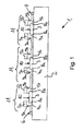
- a resistive layer 3 a contact layer 4a, 4b adjacent thereto at a first boundary surface 8a, 8b, and a passivation layer adjacent to the contact layer 4a, 4b at a second boundary surface 9a, 9b 5a, 5b provided.
- these layer arrangements 11 are connected in series between the terminals 6, 7 in such a way that the electrical current applied by the current source to the terminals 6, 7 passes through all the first boundary surfaces 8a, 8b and through at least two of the second boundary surfaces 9a, 9b flows through.
- the passivation layers 5a, 5b are made of an electrically conductive material, preferably a noble metal, preferably of gold, and each have a portion which serves as an electrical connection 6, 7. At the terminals 6, 7, a power source of an evaluation device not shown in the drawing is connected.
- the substrate may be an electrically conductive substrate having passivation layers, a semiconductor substrate, such as a semiconductor substrate. a silicon substrate, or an electrically insulating substrate, for example, a ceramic substrate or a plastic substrate.
- each contact layer 4a, 4b is in each case arranged directly on the substrate 2.
- the contact layers 4a, 4b each have an approximately stepped or stepped course between the partial region covering the resistance layer 3 and the partial region adjoining the substrate 2.
- the passivation layer 5a, 5b completely covers the contact layer 4a, 4b assigned to it.
- the passivation layer 5a, 5b follows the step-shaped or stepped shape of the underlying contact layer 4a, 4b.
- the passivation layer 5a, 5b and the contact layer 4a, 4b are each formed as a thin film.
- the layer thickness of the passivation layer 5a, 5b and the contact layer 4a, 4b may be, for example, about 100 ⁇ m.
- Fig. 2 can still be seen that the passivation layer 5a, 5b and the contact layer 4a, 4b at the terminals 6, 7 and the resistive layer 3 overlapping portion each having a greater width than in a between the terminals 6, 7 and the resistive layer 3 overlapping portion located section.
- the resistive layer 3 has a surface region 10 adjoining the atmosphere. This surface region 10 directly adjoins the first boundary surface 8a, 8b located between the resistive layer 3 and the respective contact layer 4a, 4b.
- gaseous hydrogen molecules H 2 located in the vicinity of the surface region 10 can be adsorbed to the surface region 10 in the form of hydrogen atoms H ad .
- the hydrogen atoms H ad are absorbed by the resistance layer 3 and are incorporated therein.
- the absorbed hydrogen atoms H ab diffuse to the first boundary surfaces 8 a, 8 b and possibly to the second boundary surfaces 9 a, 9 b.
- the electrical connections 6, 7 are connected to an evaluation device not shown in detail in the drawing, which is designed as a state of charge indicator for the hydrogen storage.
- the evaluation device can be integrated into the substrate 2 as an electronic circuit.
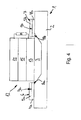
- the fuel cell is configured as a layer stack which has two electrode layers 13, 14 and a membrane layer 15 located therebetween.
- a first electrode layer 1 3 serves as a cathode and a second, to an oxygen-containing Atmosphere adjacent electrode layer 14 as an anode.
- the membrane layer 15 is designed as a polymer electrolyte membrane.
- the layer stack is arranged on the resistance layer 3 between the first boundary surfaces 8a, 8b. Between the electrode layers 13, 14 is an electrical voltage can be tapped.
Landscapes
- Chemical & Material Sciences (AREA)
- Health & Medical Sciences (AREA)
- Life Sciences & Earth Sciences (AREA)
- Analytical Chemistry (AREA)
- General Health & Medical Sciences (AREA)
- Pathology (AREA)
- Immunology (AREA)
- Physics & Mathematics (AREA)
- Engineering & Computer Science (AREA)
- Biochemistry (AREA)
- General Physics & Mathematics (AREA)
- Combustion & Propulsion (AREA)
- Medicinal Chemistry (AREA)
- Food Science & Technology (AREA)
- Chemical Kinetics & Catalysis (AREA)
- Electrochemistry (AREA)
- Investigating Or Analyzing Materials By The Use Of Electric Means (AREA)
- Investigating Or Analyzing Materials By The Use Of Fluid Adsorption Or Reactions (AREA)
Description
- Die Erfindung betrifft einen resistiven Wasserstoffsensor nach dem Oberbegriff von Anspruch 1.
- Ein derartiger resistiver Wasserstoffsensor ist aus
US-A 4 953 387 bekannt. Er weist auf einem Substrat vier nebeneinander angeordnete Kontaktschichten mit jeweils einem elektrischen Anschluss auf Die Kontaktschichten sind von einer Widerstandsschicht aus Palladium überdeckt, welche sich durchgehend über die Kontaktschichten erstreckt. Die Widerstandsschicht ändert bei Wasserstoffaufnahme ihren elektrischen Widerstand. Die Widerstandsschicht hat Grenzflächen, an denen sie an die Kontaktschichten angrenzt. Um den Einfluss der Kontaktwiderstande auf das Messergebnis zu reduzieren, wird eine sogenannte Vierpunktmessung durchgeführt, bei der in die beiden äußeren Kontaktschichten ein Strom eingespeist wird und an den beiden inneren Kontaktschichten die aus dem Stromfluss resultierende Spannung gemessen wird. - Aus Sakamoto, Y. et al.: "Electrical restistance measurements as a function of composition of palladium-hydrogen(deuterium) systems by a gas phase method", J. Phys.: Condens. Matter 8 (1996), Seiten 3399-3411 ist ferner eine Wasserstoffsensor bekannt, der als Widerstandsschicht eine Palladium-Folie mit einer Dicke von 50-60 µm aufweist, die in Streifen von ca. 2 mm x 5 mm geschnitten ist. Die Widerstandsschicht ist in einem Reaktionsgefäß aus Edelstahl angeordnet, das über Zuleitungen mit einem Wasserstoff- und einem Deuterium-Vorratsbehälter verbunden ist. An die Widerstandsschicht sind Nickeldrähte mit einem Durchmesser von etwa 0,3 mm angeschweißt, welche die Widerstandsschicht mit außerhalb des Reaktionsgefäßes angeordneten elektrischen Anschlüssen verbinden. Als elektrische Isolierung für die Nickeldrähte sind Glasröhrchen vorgesehen, die mit dem Reaktionsgefäß verbunden sind. Bei einer Temperatur von 273 K beträgt der elektrische Widerstand der wasserstoffrelen Palladium-Folie etwa 4,682±0,1 067 mΩ Wird die Palladium-Folie bei Raumtemperatur einer WasserstoffAtmosphäre mit einem Druck von einem bar ausgesetzt, so ändert sich ihr spezifischer Widerstand um circa 80% im Vergleich zu einer wasserstoffreien Palladium-Folie. Der Wasserstoffsensor hat den Nachteil, dass der elektrische Widerstand der Palladium-Folie nur relativ gering ist, so dass der Widerstand der Zuleitungen, welche die Anschlüsse mit der Palladium-Folie verbinden, wesentlich in die Messung mit eingeht. Da der elektrische Widerstand der Zuleitungen mit abnehmendem Leitungsquerschnitt zunimmt, ist eine Miniaturisierung des Wasserstoffsensors nur begrenzt möglich. Wird der Querschnitt der Zuleitungen zu gering dimensioniert, wird der elektrische Widerstand zwischen den Anschlüssen des Wasserstoffsensors im Wesentlichen nur noch durch die Zuleitungen bestimmt. Auch können Temperaturveränderungen, die den elektrischen Widerstand der Palladium-Folie und der Zuleitungen beeinflussen, zu Fehlern bei der Messung führen.
- Aus Wang, Min et al.: "Palladium-silver thin film for hydrogen sensing", Sensors and Actuators B 123 (2007), Seiten 101-106 ist außerdem ein Wasserstoffsensor bekannt, der eine Widerstandsschicht aus einer Palladium-Silber-Legierung aufweist, die mittels eines Dünnschichtprozesses auf ein Keramiksubstrat aufgebracht ist. Gegenüber einer Widerstandsschicht aus reinem Palladium ermöglicht die Polladium-Silber-Legierung eine größere Stabilität bei der Wasserstoffeinlagerung. Um den elektrischen Widerstand zu erhöhen, ist die Widerstandsschicht mäanderförmig strukturiert. Ungünstig ist dabei jedoch, dass die Widerstandsschicht einen relativ großen Oberflächenbereich auf dem Substrat bedeckt. Trotz der mäanderförmigen Ausgestaltung ist auch bei diesem Wasserstoffsensor der elektrische Widerstand der Widerstandsschicht noch relativ gering.
- Es besteht deshalb die Aufgabe, einen Wasserstoffsensor der eingangs genannten Art zu schaffen, der bei kompakten Abmessungen eine hohe Messempfindlichkeit ermöglicht.
- Diese Aufgabe wird mit den Merkmalen des Anpruchs 1 gelöst.
- In vorteilhafter Weise ändert sich bei einer Veränderung der Wassersffokonzentratlon zusätzlich zum elektrischen Widerstand der Widerstandsschicht auch der Kontakfwiderstand an der Grenzfläche zwischen der Widerstandsschicht und der Kontaktschicht. Dadurch ergibt sich eine deutliche Veränderung des elektrischen Widerstands zwischen den Anschlüssen des Wasserstoffsensors und somit eine hohe Messempfindlichkeit Der Wasserstoffsensor kann mit aus der Halbleiterfertigungstechnlk bekannten Prozessschritten mit kompakten Abmessungen hergestellt werden, indem die Widerstandsschicht auf ein Substrat aufgebracht wird, beispielsweise ein Siliziumsubstrat. Augrund der im Vergleich zu herkömmlichen resistiven Wasserstoffsensoren erhöhten Empfindlichkeit kann die Widerstands-schicht über Leiterbahnen relativ geringen Querschnitts mit den elektrischen Anschlüssen verbunden sein. Dabei sind die Leiterbahnen bevorzugt auf und/oder in das Substrat integriert. Der Wasserstoffsensor ist dadurch kostengünstig herstellbar und ermöglicht kompakte Abmessungen. Das mindestens eine chemische Element der vierten Nebengruppe kann insbesondere Hafnium, oder Zirkon sein. Der Wasserstoffsensor ermöglicht ein hohes Messsignal, wobei das Gesamtmesssignal der Summe der an den einzelnen Schichtanordnungen auftretenden Teilmesssignale entspricht.
- Bei einer bevorzugten Ausführungsform der Erfindung besteht die Kontaktschicht aus Titan oder enthält Titan und/oder eine titanhaltige chemische Verbindung. Mit einer solchen Kontaktschicht kann eine besonders hohe Messempfindlichkeit erzielt werden. Außerdem ist Titan vergleichsweise kostengünstig verfügbar.
- Bei einer vorteilhaften Ausgestaltung der Erfindung ist die Widerstandsschicht auf einem Substrat angeordnet, wobei die Kontaktschicht die Widerstandsschicht zumindest bereichsweise derart überdeckt, dass mindestens ein Teilbereich der Widerstandsschicht zwischen der Grenzfläche und dem Substrat angeordnet ist. Die aus der Widerstandsschicht und der Kontaktschicht bestehende Schichtenfolge ermöglicht dann auch bei geringen Schichtdicken eine relativ groBe Grenzfläche zwischen der Widerstandsschicht und der Kontaktschicht.
- Zweckmäßigerweise ist die Kontaktschicht von einer Passivierungsschicht überdeckt. Dadurch wird bei einem Kontakt des Wasserstoffsensors mit Luftsauerstoff eine Oxidation der Kontaktschicht vermieden.
- Die Widerstandsschicht besteht bevorzugt aus Palladium oder weist eine palladiumhaltige Legierung und/oder eine palladiumhaltige chemische Verbindung auf Der Wasserstoffsensor ermöglicht dann eine noch größereMessempfindlichkeit.
- Bei einer anderen vorteilhaften Ausgestaltung der Erfindung enthält die Widerstandsschicht eine zur Einlagerung von Wasserstoff geeignete chemische Verbindung zwischen einem ersten chemischen Element A und einem zweiten chemischen Element B, die vom Typ AB2 oder AB5 ist. Auch mit einer solchen Widerstandsschicht kann eine hohe Messempfindlichkeit erreicht werden.
- Vorteilhaft ist, wenn die Passivierungsschicht eine metallische Schicht ist, die an einer zweiten Grenzfläche an die Widerstandsschicht angrenzt, und wenn die Passivierungsschicht zwischen den elektrischen Anschlüssen mit der Kontaktschicht und der Widerstandsschicht in Reihe geschaltet ist und vorzugsweise aus Gold besteht. Bei einem Stromfluss zwischen den elektrischen Anschlüssen tritt dann an der zwischen der Widerstandsschicht und der Kontaktschicht gebildeten ersten Grenzfläche und/oder der zwischen der Kontaktschicht und der Passivierungsschicht gebildeten zweiten Grenzfläche ein von der Wasserstoffkonzentration in der Widerstandsschicht abhängiger Spannungsabfall auf Der Wasserstoffsensor ermöglicht dadurch an den elektrischen Anschlüssen ein noch größeres Messsignal.
- Bei einer bevorzugten Ausführungsform der Erfindung ist die Kontaktschicht als Dünnfilm ausgebildet, der eine Schichtdicke von weniger als 300 µm, insbesondere weniger als 200 µm und bevorzugt weniger als 100 µm aufweist. Der Wasserstoff sensor kann dann mit Standardprozessen der Halbleiterfertigungstechnik kostengünstig beispielsweise auf einem Substrat aus Silizium hergestellt werden. Der Wasserstoffsensor ermöglicht dadurch sehr kompakte Abmessungen.
- Bei einer möglichen Ausführungsform der Erfindung ist zumindest ein Teilbereich der Kontaktschicht zwischen der Widerstandsschicht und dem Substrat angeordnet. Die Widerstandsschicht dient dabei außer zur Generierung des Messsignals auch als Passivierung für die Kontakschicht.
- Bei einer bevorzugten Ausgestaltung der Erfindung weist die Widerstandsschicht mindestens einen an die Atmosphäre angrenzenden Oberflächenbereich auf, wobei dieser Oberflächenbereich vorzugsweise seitlich an die zwischen der Widerstandsschicht und der Kontaktschicht befindliche Grenzfläche angrenzt. Der Wasserstoffsensor kann dann zum Detektieren von in der Umgebung befindlichem Wasserstoffgas verwendet werden. Durch eine kontinuierliche Messung des elektrischen Widerstands zwischen den Anschlüssen des Wasserstoffsensors kann eindeutig auf den Wasserstoffpartialdruck in der Umgebung geschlossen werden. Wenn der an die Atmosphäre angrenzende Oberflächenbereich zu der Grenzfläche benachbart ist, kann der Wasserstoff über kurze Diffusionswege von dem Oberflächenbereich zu der Grenzfläche gelangen. Das Messsignal des Wasserstoff sensors reagiert dann schnell auf Änderungen des Wasserstoffpartialdrucks.
- Bei einer anderen vorteilhaften Ausgestaltung der Erfindung ist die Widerstandsschicht ein mit einer Brennstoffzelle verbundener Wasserstoffspeicher und die elektrischen Anschlüsse sind mit einer Auswerteeinrichtung verbunden, die als Ladezustandsanzeige für den Wasserstoffspeicher ausgebildet ist. Dabei weist die Auswerteeinrichtung vorzugsweise eine Anzeige für Ladezustand auf Somit kann auf einfache Weise der Ladezustand des Wasserstoffspeichers überprüft und/oder die Menge des in dem Wasserstoffspeicher eingelagerten Wasserstoffs gemessen werden.
- Vorteilhaft ist, wenn die Brennstoffzelle einen Schichtstapel, bestehend zumindest aus zwei Elektrodenschichten und einer dazwischen befindlichen Membranschicht aufweist, und wenn die Widerstandsschicht zumindest bereichsweise zwischen diesem Schichtstapel und dem Substrat angeordnet ist. Dadurch ergibt sich eine sehr kompakte Anordnung, bei der die Brennstoffzelle zum Einsparen von Chipfläche auf dem Wasserstoffsensor angeordnet ist. Die Membranschicht ist eine ionenleitende Schicht, bevorzugt eine Polymer-Elektrolytmembran.
- Nachfolgend sind Ausführungsbeispiele der Erfindung näher erläutert. Es zeigt:
- Fig. 1
- einen Querschnitt durch ein erstes Ausführungsbeispiel des Wasserstoffsensors,
- Fig. 2
- eine Aufsicht auf den in
Fig. 1 gezeigten Wasserstoffsensor,und - Fig. 3
- eine schematische Darstellung, die Adsorbieren von Wasserstoff an die Oberfläche einer Palladiumschicht und Absorbieren von Wasserstoff die Palladiumschicht des Wasserstoffgassensor zeigt, und
- Fig. 4
- einen Querschnitt durch ein zweites, in eine Berennstoffzelle integriertes Ausführungsbeispiel des Wasserstoffsensors, wobei ein an der Brennstoffzelle angeschlossener elektrischer Verbraucher schematisch durch ein Widerstandssymbol dargestellt ist.
- Bei dem in
Fig.1 und2 gezeigten Ausführungsbeispiel sind auf einem Substrat 2 mehrere der Schichtanordnungen 11, jeweils bestehend aus einer Widerstandsschicht 3, einer daran an einer ersten Grenzfläche 8a, 8b angrenzenden Kontaktschicht 4a, 4b und einer an einer zweiten Grenzfläche 9a, 9b an die Kontaktschicht 4a, 4b angrenzenden Passivierungsschicht 5a, 5b vorgesehen. Deutlich ist erkennbar, dass diese Schichtanordnungen 11 zwischen den Anschlüssen 6, 7 derart in Reihe geschaltet sind, dass der von der Stromquelle an die Anschlüsse 6, 7 angelegte elektrische Strom durch alle erste Grenzflächen 8a, 8b und durch mindestens zwei der zweiten Grenzflächen 9a, 9b hindurchfließt. - Die Passivierungsschichten 5a, 5b bestehen aus einem elektrisch leitfähigen Material, bevorzugt einem Edelmetall, vorzugsweise aus Gold und haben jeweils einen Teilbereich, der als elektrischer Anschluss 6, 7 dient. An den Anschlüssen 6, 7 ist eine Stromquelle einer in der Zeichnung nicht näher dargestellten Auswerteeinrichtung angeschlossen. Das Substrat kann ein elektrisch leifähiges Substrat mit Passivierungsschichten, ein Halbleitersubstrat, wie z.B. ein Siliziumsubstrat, oder ein elektrisch isolierendes Substrat, beispielsweise ein Keramiksubstrat oder ein Kunststoffsubstrat sein.
- In
Fig. 1 und2 ist erkennbar, dass die Grenzflächen 8a, 8b an voneinander beabstandeten Randbereichen der Widerstandsschicht 3 angeordnet sind, und dass die Kontaktschichten 4a, 4b jeweils einen dieser Randbereiche mit einem Teilbereich überdecken. Ein weiterer Teilbereich jeder Kontaktschicht 4a, 4b ist jeweils direkt auf dem Substrat 2 angeordnet. Zwischen dem die Widerstandsschicht 3 überdeckenden Teilbereich und dem an das Substart 2 angrenzenden Teilbereich weisen die Kontaktschichten 4a, 4b jeweils einen etwa stufen- oder absatzförmigen Verlauf auf. - Die Passivierungsschicht 5a, 5b überdeckt die ihr zugeordnete Kontaktschicht 4a, 4b jeweils vollständig. Dabei folgt die Passivierungsschicht 5a, 5b dem stufen- oder absatzförmigen Verlauf der darunter liegenden Kontaktschicht 4a, 4b. Die Passivierungsschicht 5a, 5b und die Kontaktschicht 4a, 4b sind jeweils als Dünnfilm ausgebildet. Die Schichtdicke der Passivierungsschicht 5a, 5b und der Kontaktschicht 4a, 4b kann beispielsweise etwa 100 µm betragen.
- In
Fig. 2 ist noch erkennbar, dass die Passivierungsschicht 5a, 5b und die Kontaktschicht 4a, 4b an den Anschlüssen 6, 7 und dem die Widerstandsschicht 3 überdeckenden Teilbereich jeweils eine größer Breite aufweisen als in einem zwischen den Anschlüssen 6, 7 und dem die Widerstandsschicht 3 überdeckenden Teilbereich befindlichen Abschnitt. - Zwischen den Kontaktschichten 4a, 4b hat die Widerstandsschicht 3 einen an die Atmosphäre angrenzenden Oberflächenbereich 10. Dieser Oberflächenbereich 10 grenzt seitilch direkt an die zwischen der Widerstandsschicht 3 und der betreffenden Kontaktschicht 4a, 4b befindliche erste Grenzfläche 8a, 8b an.
- In
Fig. 3 ist erkennbar, dass in der Umgebung des Oberflächenbereichs 10 befindliche gasförmige Wasserstoffmoleküle H2 in Form von Wasserstoffatomen Had an den Oberflächenbereich 10 adsorbiert werden können. Die Wasserstoffatome Had werden von der Widerstandsschicht 3 absorbiert und lagern sich in dieser ein. In der Widerstandsschicht 3 diffundieren die absorbierten Wasserstoffatome Hab zu den ersten Grenzflächen 8a, 8b und ggf. den zweiten Grenzflächen 9a, 9b. - Bei dem in
Fig. 4 gezeigten Ausführungsbeispiel ist die Widerstandsschicht als Dickschicht ausgestaltet, die als Wasserstoffspeicher für eine Brennstoffzelle 12 dient Die elektrischen Anschlüsse 6, 7 sind mit einer in der Zeichnung nicht näher dargestellten Auswerteeinrichtung verbunden, die als Ladezustandsanzeige für den Wasserstoffspeicher ausgebildet ist. Die Auswerteeinrichtung kann als elektronische Schaltung in das Substrat 2 integriert sein. - Die Brennstoffzelle ist als Schichtstapel ausgestaltet, der zwei Elektrodenschichten 13, 14 und eine dazwischen befindlichen Membranschicht 15 aufweist. Eine erste Elektrodenschicht 1 3 dient als Kathode und eine zweite, an eine sauerstoffhaltige Atmosphäre angrenzende Elektrodenschicht 14 als Anode. Die Membranschicht 15 ist als Polymer-Elektrolytmembran ausgestaltet. Der Schichtstapel ist auf der Widerstandsschicht 3 zwischen den ersten Grenzflächen 8a, 8b angeordnet. Zwischen den Elektrodenschichten 13, 14 liegt eine elektrische Spannung abgreifbar.
Claims (12)
- Resistiver Wasserstoffsensor (1), der wenigstens zwei elektrische Anschlüsse (6, 7) und mindestens eine Widerstandsschicht (3) aufweist, die bei Wasserstoffaufhahme ihren elektrischen Widerstand ändert, wobei die elektrischen Anschlüsse (6, 7) über die Widerstandsschicht (3) miteinander verbunden sind, wobei die Widerstandsschicht (3) an wenigstens einer Grenzfläche (8a, 8b) an eine Kontaktschicht (4a, 4b) angrenzt, die mindestens ein chemisches Element der vierten Nebengruppe und/oder Kohlenstoff enthält, und wobei die Kontaktschicht (4a, 4b) zwischen den elektrischen Anschlüssen (6, 7) mit der Widerstandsschicht (3) in Reihe geschaltet ist, dadurch gekennzeichnet, dass auf dem Substrat (2) mindestens zwei der Schichtanordnungen (11), jeweils bestehend zumindest aus der Widerstandsschicht (3) und der daran angrenzenden Kontaktschicht (4a, 4b) und einer an diese angrenzenden Passivierungsschicht (5a, 5b) angeordnet sind, und dass diese Schichtanordnungen (11) derart zwischen den elektrischen Anschlüssen (6, 7) in Reihe geschaltet sind, dass die Widerstandsschichten (3) voneinander beabstandet sind.
- Resistiver Wasserstoffsensor (1) nach Anspruch 1, dadurch gekennzeichnet, dass die Kontaktschicht (4a, 4b) aus Titan besteht oder Titan und/oder eine titanhaltige chemische Verbindung enthält.
- Resistiver Wasserstoffsensor (1) nach Anspruch 1 oder 2, dadurch gekennzeichnet, dass die Widerstandsschicht (3) auf einem Substrat (2) angeordnet ist, und dass die Kontaktschicht (4a, 4b) die Widerstandsschicht (3) zumindest bereichsweise derart überdeckt, dass mindestens ein Teilbereich der Widerstandsschicht (3) zwischen der Grenzfläche (8a, 8b) und dem Substrat (2) angeordnet ist.
- Resistiver Wasserstoffsensor (1) nach einem der Ansprüche 1 bis 3, dadurch gekennzeichnet, dass die Kontaktschicht (4a, 4b) von einer Passivierungsschicht (5a, 5b) überdeckt ist.
- Resistiver Wasserstoffsensor (1) nach einem der Ansprüche 1 bis 4, dadurch gekennzeichnet, dass die Widerstandsschicht (3) aus Palladium besteht, eine palladiumhaltige Legierung und/oder eine palladiumhaltige chemische Verbindung aufweist.
- Resistiver Wasserstoffsensor (1) nach einem der Ansprüche 1 bis 5, dadurch gekennzeichnet, dass die Widerstandsschicht (3) eine zur Einlagerung von Wasserstoff geeignete chemische Verbindung zwischen einem ersten chemischen Element A und einem zweiten chemischen Element B enthält, die vom Typ AB2 oder AB5 ist.
- Resistiver Wasserstoffsensor (1) nach einem der Ansprüche 1 bis 6, dadurch gekennzeichnet, dass die Passivierungsschicht (5a, 5b) eine metallische Schicht ist, die an einer zweiten Grenzfläche (9a, 9b) an die Widerstandsschicht (3) angrenzt, und dass die Passivierungsschicht (5a, 5b) zwischen den elektrischen Anschlüssen (6, 7) mit der Kontaktschicht (4a, 4b) und der Widerstandsschicht (3) in Reihe geschaltet ist und vorzugsweise aus Gold besteht.
- Resistiver Wasserstoffsensor (1) nach einem der Ansprüche 1 bis 7, dadurch gekennzeichnet, dass die Kontaktschicht (4a, 4b) als Dünnfilm ausgebildet ist, der eine Schichtdicke von weniger als 300 µm, insbesondere weniger als 200 µm und bevorzugt weniger als 100 µm aufweist.
- Resistiver Wasserstoffsensor (1) nach einem der Ansprüche 1 bis 8, dadurch gekennzeichnet, dass zumindest ein Teilbereich der Kontaktschicht (4a, 4b) zwischen der Widerstandsschicht (3) und dem Substrat (2) angeordnet ist.
- Resistiver Wasserstoffsensor (1) nach einem der Ansprüche 1 bis 9, dadurch gekennzeichnet, dass die Widerstandsschicht (3) mindestens einen an die Atmosphäre angrenzenden Oberflächenbereich (10) aufweist, und dass dieser Oberflächenbereich (10) vorzugsweise seitlich an die zwischen der Widerstandsschicht (3) und der Kontaktschicht (4a, 4b) befindliche erste Grenzfläche (8a, 8b) angrenzt.
- Resistiver Wasserstoffsensor (1) nach einem der Ansprüche 1 bis 10, dadurch gekennzeichnet, dass die Widerstandsschicht (3) ein mit einer Brennstoffzelle (12) verbundener Wasserstoffspeicher ist und dass die elektrischen Anschlüsse (6, 7) mit einer Auswerteeinrichtung verbunden sind, die als Ladezustandsanzeige für den Wasserstoffspeicher ausgebildet ist.
- Resistiver Wasserstoffsensor (1) nach einem der Ansprüche 1 bis 11, dadurch gekennzeichnet, dass die Brennstoffzelle (12) einen Schichtstapel, bestehend zumindest aus zwei Elektrodenschichten (13, 14) und einer dazwischen befindlichen Membranschicht (15) aufweist, und dass die Widerstandsschicht (3) zumindest bereichsweise zwischen diesem Schichtstapel und dem Substrat (2) angeordnet ist.
Priority Applications (2)
| Application Number | Priority Date | Filing Date | Title |
|---|---|---|---|
| EP08001491.3A EP2083262B1 (de) | 2008-01-28 | 2008-01-28 | Resistiver Wasserstoffsensor |
| US12/360,589 US9664633B2 (en) | 2008-01-28 | 2009-01-27 | Resistive hydrogen sensor |
Applications Claiming Priority (1)
| Application Number | Priority Date | Filing Date | Title |
|---|---|---|---|
| EP08001491.3A EP2083262B1 (de) | 2008-01-28 | 2008-01-28 | Resistiver Wasserstoffsensor |
Publications (2)
| Publication Number | Publication Date |
|---|---|
| EP2083262A1 EP2083262A1 (de) | 2009-07-29 |
| EP2083262B1 true EP2083262B1 (de) | 2014-05-07 |
Family
ID=39512651
Family Applications (1)
| Application Number | Title | Priority Date | Filing Date |
|---|---|---|---|
| EP08001491.3A Ceased EP2083262B1 (de) | 2008-01-28 | 2008-01-28 | Resistiver Wasserstoffsensor |
Country Status (2)
| Country | Link |
|---|---|
| US (1) | US9664633B2 (de) |
| EP (1) | EP2083262B1 (de) |
Families Citing this family (8)
| Publication number | Priority date | Publication date | Assignee | Title |
|---|---|---|---|---|
| CN102012385B (zh) * | 2010-09-16 | 2012-08-15 | 中国石油大学(华东) | 一种具有氢气敏感效应的钯/碳/硅异质结材料 |
| JP2017028079A (ja) * | 2015-07-22 | 2017-02-02 | イビデン株式会社 | プリント配線板の製造方法およびプリント配線板 |
| WO2017205146A1 (en) * | 2016-05-27 | 2017-11-30 | Carrier Corporation | Gas detection device and method of manufacturing the same |
| JP6840170B2 (ja) * | 2016-12-15 | 2021-03-10 | ヌヴォトンテクノロジージャパン株式会社 | 水素検出装置、燃料電池自動車、水素漏洩監視システム、複合センサモジュール、水素検出方法、およびプログラム |
| EP3754329B1 (de) * | 2019-06-21 | 2023-07-26 | Materion GmbH | Wasserstoffsensor und verfahren zu dessen herstellung, messvorrichtung und verfahren zum messen einer wasserstoffkonzentration |
| US12188914B2 (en) * | 2020-11-06 | 2025-01-07 | Trace Sensing Technologies Inc. | Decoupled thermodynamic sensing system |
| US11143641B1 (en) * | 2021-04-05 | 2021-10-12 | Vivante Health, Inc. | Gas sensor calibration method |
| WO2025159102A1 (ja) * | 2024-01-25 | 2025-07-31 | ヌヴォトンテクノロジージャパン株式会社 | 水素検知装置及び水素検知方法 |
Family Cites Families (8)
| Publication number | Priority date | Publication date | Assignee | Title |
|---|---|---|---|---|
| US4224280A (en) * | 1977-07-18 | 1980-09-23 | Fuji Electric Co., Ltd. | Carbon monoxide detecting device |
| US4953387A (en) | 1989-07-31 | 1990-09-04 | The Regents Of The University Of Michigan | Ultrathin-film gas detector |
| JP3924188B2 (ja) * | 2002-03-20 | 2007-06-06 | 三菱重工業株式会社 | 水素ガス検出装置及びその製造方法 |
| US7237429B2 (en) * | 2002-08-30 | 2007-07-03 | Nano-Proprietary, Inc. | Continuous-range hydrogen sensors |
| US7287412B2 (en) * | 2003-06-03 | 2007-10-30 | Nano-Proprietary, Inc. | Method and apparatus for sensing hydrogen gas |
| US20070125153A1 (en) * | 2005-10-21 | 2007-06-07 | Thomas Visel | Palladium-Nickel Hydrogen Sensor |
| DE102004011554A1 (de) | 2004-03-08 | 2005-09-29 | Micronas Gmbh | Brennstoffzellenanordnung |
| US7041591B1 (en) * | 2004-12-30 | 2006-05-09 | Phoenix Precision Technology Corporation | Method for fabricating semiconductor package substrate with plated metal layer over conductive pad |
-
2008
- 2008-01-28 EP EP08001491.3A patent/EP2083262B1/de not_active Ceased
-
2009
- 2009-01-27 US US12/360,589 patent/US9664633B2/en active Active
Also Published As
| Publication number | Publication date |
|---|---|
| US9664633B2 (en) | 2017-05-30 |
| EP2083262A1 (de) | 2009-07-29 |
| US20090188316A1 (en) | 2009-07-30 |
Similar Documents
| Publication | Publication Date | Title |
|---|---|---|
| EP2083262A1 (de) | Resistiver Wasserstoffsensor | |
| DE69713698T2 (de) | Gasfühler | |
| EP2089696B1 (de) | Verfahren zur Herstellung eines Sensors und nach diesem Verfahren hergestellter Sensor | |
| WO2001042776A1 (de) | Kapazitiver sensor | |
| CH676153A5 (de) | ||
| EP2867904A1 (de) | Widerstand, insbesondere niederohmiger strommesswiderstand | |
| DE102007059652A1 (de) | Gassensor mit einer verbesserten Selektivität | |
| WO2010136351A2 (de) | Sensorelement | |
| DE102016220353A1 (de) | Gassensor | |
| DE19960329C2 (de) | Elektrochemischer Meßfühler | |
| DE19941420A1 (de) | Elektrischer Widerstand mit wenigstens zwei Anschlußkontaktfeldern auf einem Substrat mit wenigstens einer Ausnehmung sowie Verfahren zu dessen Herstellung | |
| WO2008107229A1 (de) | Gassensor zur messung einer gaskomponente in einem gasgemisch | |
| DE4021929A1 (de) | Sensor | |
| DE102005010613B4 (de) | Platinwiderstands-Temperatursensor | |
| DE10208767C1 (de) | Meßanordnung und Verfahren zur Bestimmung der Permeabilität einer Schicht für eine korrodierende Substanz sowie Bauelemente mit dieser Meßanordnung | |
| EP0645621A2 (de) | Sensoranordnung | |
| DE69422878T2 (de) | Nachweis von reaktiven Gasen | |
| EP1782048A1 (de) | Gassensor und verfahren herstellung einens gassensors | |
| EP1621882B1 (de) | Verfahren zur Erfassung brennbarer Gase, insbesondere zur Erfassung von Wasserstoff | |
| DE2831400A1 (de) | Kohlenmonoxid-sensor | |
| DE4431456C2 (de) | In Dick- oder Dünnschichttechnik hergestellter Gassensor | |
| EP2141491A1 (de) | Gassensor | |
| EP4729905A1 (de) | Sensorelement mit überspannungsschutz | |
| EP1463933A1 (de) | Sensorelement | |
| DE102024210491A1 (de) | Verfahren zur Bestimmung der Art und/oder der Konzentration einer oxidierbaren Gaskomponente in einem sauerstoffhaltigen Gasgemisch |
Legal Events
| Date | Code | Title | Description |
|---|---|---|---|
| PUAI | Public reference made under article 153(3) epc to a published international application that has entered the european phase |
Free format text: ORIGINAL CODE: 0009012 |
|
| AK | Designated contracting states |
Kind code of ref document: A1 Designated state(s): AT BE BG CH CY CZ DE DK EE ES FI FR GB GR HR HU IE IS IT LI LT LU LV MC MT NL NO PL PT RO SE SI SK TR |
|
| AX | Request for extension of the european patent |
Extension state: AL BA MK RS |
|
| 17P | Request for examination filed |
Effective date: 20100129 |
|
| 17Q | First examination report despatched |
Effective date: 20100224 |
|
| AKX | Designation fees paid |
Designated state(s): CH DE FR GB IT LI NL |
|
| GRAP | Despatch of communication of intention to grant a patent |
Free format text: ORIGINAL CODE: EPIDOSNIGR1 |
|
| INTG | Intention to grant announced |
Effective date: 20140129 |
|
| GRAS | Grant fee paid |
Free format text: ORIGINAL CODE: EPIDOSNIGR3 |
|
| GRAA | (expected) grant |
Free format text: ORIGINAL CODE: 0009210 |
|
| AK | Designated contracting states |
Kind code of ref document: B1 Designated state(s): CH DE FR GB IT LI NL |
|
| REG | Reference to a national code |
Ref country code: GB Ref legal event code: FG4D Free format text: NOT ENGLISH |
|
| REG | Reference to a national code |
Ref country code: DE Ref legal event code: R096 Ref document number: 502008011700 Country of ref document: DE Effective date: 20140612 |
|
| REG | Reference to a national code |
Ref country code: NL Ref legal event code: VDEP Effective date: 20140507 |
|
| REG | Reference to a national code |
Ref country code: DE Ref legal event code: R097 Ref document number: 502008011700 Country of ref document: DE |
|
| PG25 | Lapsed in a contracting state [announced via postgrant information from national office to epo] |
Ref country code: NL Free format text: LAPSE BECAUSE OF FAILURE TO SUBMIT A TRANSLATION OF THE DESCRIPTION OR TO PAY THE FEE WITHIN THE PRESCRIBED TIME-LIMIT Effective date: 20140507 |
|
| PLBE | No opposition filed within time limit |
Free format text: ORIGINAL CODE: 0009261 |
|
| STAA | Information on the status of an ep patent application or granted ep patent |
Free format text: STATUS: NO OPPOSITION FILED WITHIN TIME LIMIT |
|
| 26N | No opposition filed |
Effective date: 20150210 |
|
| PG25 | Lapsed in a contracting state [announced via postgrant information from national office to epo] |
Ref country code: IT Free format text: LAPSE BECAUSE OF FAILURE TO SUBMIT A TRANSLATION OF THE DESCRIPTION OR TO PAY THE FEE WITHIN THE PRESCRIBED TIME-LIMIT Effective date: 20140507 |
|
| REG | Reference to a national code |
Ref country code: DE Ref legal event code: R097 Ref document number: 502008011700 Country of ref document: DE Effective date: 20150210 |
|
| REG | Reference to a national code |
Ref country code: FR Ref legal event code: PLFP Year of fee payment: 9 |
|
| REG | Reference to a national code |
Ref country code: FR Ref legal event code: PLFP Year of fee payment: 10 |
|
| REG | Reference to a national code |
Ref country code: DE Ref legal event code: R082 Ref document number: 502008011700 Country of ref document: DE Representative=s name: KOCH-MUELLER PATENTANWALTSGESELLSCHAFT MBH, DE Ref country code: DE Ref legal event code: R081 Ref document number: 502008011700 Country of ref document: DE Owner name: TDK-MICRONAS GMBH, DE Free format text: FORMER OWNER: MICRONAS GMBH, 81539 MUENCHEN, DE |
|
| REG | Reference to a national code |
Ref country code: CH Ref legal event code: PFA Owner name: TDK-MICRONAS GMBH IPR-MANAGEMENT 27, DE Free format text: FORMER OWNER: MICRONAS GMBH, DE |
|
| REG | Reference to a national code |
Ref country code: FR Ref legal event code: PLFP Year of fee payment: 11 |
|
| REG | Reference to a national code |
Ref country code: FR Ref legal event code: CD Owner name: TDK-MICRONAS GMBH, DE Effective date: 20180717 |
|
| PGFP | Annual fee paid to national office [announced via postgrant information from national office to epo] |
Ref country code: GB Payment date: 20200123 Year of fee payment: 13 |
|
| PGFP | Annual fee paid to national office [announced via postgrant information from national office to epo] |
Ref country code: CH Payment date: 20200121 Year of fee payment: 13 |
|
| PGFP | Annual fee paid to national office [announced via postgrant information from national office to epo] |
Ref country code: FR Payment date: 20200121 Year of fee payment: 13 |
|
| REG | Reference to a national code |
Ref country code: CH Ref legal event code: PL |
|
| GBPC | Gb: european patent ceased through non-payment of renewal fee |
Effective date: 20210128 |
|
| PG25 | Lapsed in a contracting state [announced via postgrant information from national office to epo] |
Ref country code: FR Free format text: LAPSE BECAUSE OF NON-PAYMENT OF DUE FEES Effective date: 20210131 |
|
| PG25 | Lapsed in a contracting state [announced via postgrant information from national office to epo] |
Ref country code: LI Free format text: LAPSE BECAUSE OF NON-PAYMENT OF DUE FEES Effective date: 20210131 Ref country code: CH Free format text: LAPSE BECAUSE OF NON-PAYMENT OF DUE FEES Effective date: 20210131 Ref country code: GB Free format text: LAPSE BECAUSE OF NON-PAYMENT OF DUE FEES Effective date: 20210128 |
|
| PGFP | Annual fee paid to national office [announced via postgrant information from national office to epo] |
Ref country code: DE Payment date: 20240719 Year of fee payment: 17 |
|
| REG | Reference to a national code |
Ref country code: DE Ref legal event code: R119 Ref document number: 502008011700 Country of ref document: DE |
|
| PG25 | Lapsed in a contracting state [announced via postgrant information from national office to epo] |
Ref country code: DE Free format text: LAPSE BECAUSE OF NON-PAYMENT OF DUE FEES Effective date: 20250801 |