EP2082989A2 - Verfahren zur Herstellung eines Sensors - Google Patents
Verfahren zur Herstellung eines Sensors Download PDFInfo
- Publication number
- EP2082989A2 EP2082989A2 EP09150363A EP09150363A EP2082989A2 EP 2082989 A2 EP2082989 A2 EP 2082989A2 EP 09150363 A EP09150363 A EP 09150363A EP 09150363 A EP09150363 A EP 09150363A EP 2082989 A2 EP2082989 A2 EP 2082989A2
- Authority
- EP
- European Patent Office
- Prior art keywords
- forming
- sensor
- silicon
- layer
- silicon layer
- Prior art date
- Legal status (The legal status is an assumption and is not a legal conclusion. Google has not performed a legal analysis and makes no representation as to the accuracy of the status listed.)
- Withdrawn
Links
- 238000000034 method Methods 0.000 title claims abstract description 103
- 238000004519 manufacturing process Methods 0.000 title claims abstract description 16
- 229910052710 silicon Inorganic materials 0.000 claims abstract description 84
- 239000010703 silicon Substances 0.000 claims abstract description 84
- XUIMIQQOPSSXEZ-UHFFFAOYSA-N Silicon Chemical compound [Si] XUIMIQQOPSSXEZ-UHFFFAOYSA-N 0.000 claims abstract description 80
- 239000000758 substrate Substances 0.000 claims abstract description 50
- 238000009413 insulation Methods 0.000 claims abstract description 17
- 239000000463 material Substances 0.000 claims abstract description 17
- 230000033001 locomotion Effects 0.000 description 38
- 230000008569 process Effects 0.000 description 30
- 239000002019 doping agent Substances 0.000 description 26
- 238000002955 isolation Methods 0.000 description 22
- 229910021420 polycrystalline silicon Inorganic materials 0.000 description 20
- 229920005591 polysilicon Polymers 0.000 description 20
- 229910052751 metal Inorganic materials 0.000 description 11
- 239000002184 metal Substances 0.000 description 11
- 230000001133 acceleration Effects 0.000 description 7
- 230000008878 coupling Effects 0.000 description 6
- 238000010168 coupling process Methods 0.000 description 6
- 238000005859 coupling reaction Methods 0.000 description 6
- 150000004767 nitrides Chemical class 0.000 description 6
- 235000012431 wafers Nutrition 0.000 description 6
- ZOXJGFHDIHLPTG-UHFFFAOYSA-N Boron Chemical compound [B] ZOXJGFHDIHLPTG-UHFFFAOYSA-N 0.000 description 5
- OAICVXFJPJFONN-UHFFFAOYSA-N Phosphorus Chemical compound [P] OAICVXFJPJFONN-UHFFFAOYSA-N 0.000 description 5
- 229910052796 boron Inorganic materials 0.000 description 5
- 239000004020 conductor Substances 0.000 description 5
- 239000011521 glass Substances 0.000 description 5
- 239000007943 implant Substances 0.000 description 5
- 229910021421 monocrystalline silicon Inorganic materials 0.000 description 5
- 229910052698 phosphorus Inorganic materials 0.000 description 5
- 239000011574 phosphorus Substances 0.000 description 5
- 238000000708 deep reactive-ion etching Methods 0.000 description 4
- 238000013461 design Methods 0.000 description 4
- 239000012212 insulator Substances 0.000 description 4
- 230000000903 blocking effect Effects 0.000 description 3
- 239000003990 capacitor Substances 0.000 description 3
- 230000003750 conditioning effect Effects 0.000 description 3
- 238000013016 damping Methods 0.000 description 3
- 230000001419 dependent effect Effects 0.000 description 3
- 238000005530 etching Methods 0.000 description 3
- 238000012545 processing Methods 0.000 description 3
- 239000007858 starting material Substances 0.000 description 3
- XKRFYHLGVUSROY-UHFFFAOYSA-N Argon Chemical compound [Ar] XKRFYHLGVUSROY-UHFFFAOYSA-N 0.000 description 2
- 230000015572 biosynthetic process Effects 0.000 description 2
- 239000002131 composite material Substances 0.000 description 2
- 238000010276 construction Methods 0.000 description 2
- 239000013078 crystal Substances 0.000 description 2
- 230000007547 defect Effects 0.000 description 2
- 238000010586 diagram Methods 0.000 description 2
- 230000010355 oscillation Effects 0.000 description 2
- 230000035945 sensitivity Effects 0.000 description 2
- 238000007669 thermal treatment Methods 0.000 description 2
- -1 C11 = 1.66 Chemical compound 0.000 description 1
- MXSJNBRAMXILSE-UHFFFAOYSA-N [Si].[P].[B] Chemical compound [Si].[P].[B] MXSJNBRAMXILSE-UHFFFAOYSA-N 0.000 description 1
- 230000002411 adverse Effects 0.000 description 1
- 238000013459 approach Methods 0.000 description 1
- 229910052786 argon Inorganic materials 0.000 description 1
- 229910052785 arsenic Inorganic materials 0.000 description 1
- RQNWIZPPADIBDY-UHFFFAOYSA-N arsenic atom Chemical compound [As] RQNWIZPPADIBDY-UHFFFAOYSA-N 0.000 description 1
- 230000008859 change Effects 0.000 description 1
- 230000002860 competitive effect Effects 0.000 description 1
- 238000011109 contamination Methods 0.000 description 1
- 230000008602 contraction Effects 0.000 description 1
- 230000003247 decreasing effect Effects 0.000 description 1
- 238000010438 heat treatment Methods 0.000 description 1
- 239000012535 impurity Substances 0.000 description 1
- 230000001939 inductive effect Effects 0.000 description 1
- 239000007788 liquid Substances 0.000 description 1
- 238000005259 measurement Methods 0.000 description 1
- 238000005459 micromachining Methods 0.000 description 1
- 238000012986 modification Methods 0.000 description 1
- 230000004048 modification Effects 0.000 description 1
- 238000012544 monitoring process Methods 0.000 description 1
- 230000037361 pathway Effects 0.000 description 1
- 230000002265 prevention Effects 0.000 description 1
- 238000009877 rendering Methods 0.000 description 1
- 230000004044 response Effects 0.000 description 1
- 238000000926 separation method Methods 0.000 description 1
- 238000004088 simulation Methods 0.000 description 1
- 239000000126 substance Substances 0.000 description 1
Images




Classifications
-
- B—PERFORMING OPERATIONS; TRANSPORTING
- B81—MICROSTRUCTURAL TECHNOLOGY
- B81C—PROCESSES OR APPARATUS SPECIALLY ADAPTED FOR THE MANUFACTURE OR TREATMENT OF MICROSTRUCTURAL DEVICES OR SYSTEMS
- B81C1/00—Manufacture or treatment of devices or systems in or on a substrate
- B81C1/00015—Manufacture or treatment of devices or systems in or on a substrate for manufacturing microsystems
- B81C1/00222—Integrating an electronic processing unit with a micromechanical structure
- B81C1/00246—Monolithic integration, i.e. micromechanical structure and electronic processing unit are integrated on the same substrate
-
- B—PERFORMING OPERATIONS; TRANSPORTING
- B81—MICROSTRUCTURAL TECHNOLOGY
- B81B—MICROSTRUCTURAL DEVICES OR SYSTEMS, e.g. MICROMECHANICAL DEVICES
- B81B3/00—Devices comprising flexible or deformable elements, e.g. comprising elastic tongues or membranes
- B81B3/0002—Arrangements for avoiding sticking of the flexible or moving parts
- B81B3/001—Structures having a reduced contact area, e.g. with bumps or with a textured surface
-
- B—PERFORMING OPERATIONS; TRANSPORTING
- B81—MICROSTRUCTURAL TECHNOLOGY
- B81B—MICROSTRUCTURAL DEVICES OR SYSTEMS, e.g. MICROMECHANICAL DEVICES
- B81B2201/00—Specific applications of microelectromechanical systems
- B81B2201/02—Sensors
- B81B2201/0228—Inertial sensors
- B81B2201/0242—Gyroscopes
-
- B—PERFORMING OPERATIONS; TRANSPORTING
- B81—MICROSTRUCTURAL TECHNOLOGY
- B81C—PROCESSES OR APPARATUS SPECIALLY ADAPTED FOR THE MANUFACTURE OR TREATMENT OF MICROSTRUCTURAL DEVICES OR SYSTEMS
- B81C2203/00—Forming microstructural systems
- B81C2203/07—Integrating an electronic processing unit with a micromechanical structure
- B81C2203/0707—Monolithic integration, i.e. the electronic processing unit is formed on or in the same substrate as the micromechanical structure
- B81C2203/0735—Post-CMOS, i.e. forming the micromechanical structure after the CMOS circuit
Definitions
- the present invention generally relates to sensors, and more particularly relates to a silicon motion sensor, such as an angular rate sensor, and a method of manufacturing a sensor.
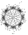
- Each of the electrode structures 20 are also configured to include balance electrodes 20C which, when energized, match the resonant peaks of the natural flexural modes of the ring 14 by inducing electrical spring softening in the ring 14 and in the springs 16, making the device responsive to Coriolis forces that occur when the sensor 10 is subjected to rotary motion about an axis perpendicular to the substrate 12.
- the balance electrodes 20C are formed by at least one pair of moving capacitive plates interdigitated with fixed plates and shown being radially inward from the drive and sensing electrodes 20A and 20B, and are electrically interconnected to electrical conductors 22. Additional balance electrodes 24 are shown disposed equiangularly around the perimeter of the ring 14, which serve to fine balance the sensing structure.
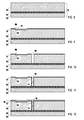
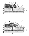
- a trench isolation scheme is utilized to form one or more trenches 112 to isolate portions of the epi layer 104 shown in FIG. 34 , as well as the sensor components.
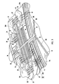
- Isolation trenches 112 may be provided as shown in FIG. 5 and may be lined with an insulator film, such as an oxide, filled with an appropriate material such as polysilicon 118, and then capped so that conductors can carry electrical signals across the isolation areas. Later, other trenches 170, such as those surrounding a delineated sensor component like the ring 14 or a compliant tether 22 are formed. The ends 40 of the filled isolation trenches 112 protrude into the trenches 170 isolating the moving element 22A as shown in FIG. 5 .
- a mask is then patterned and portions 166 of the inorganic film 162 covering the second metal 160 are etched to form exposed contact pads.
- the mask is then stripped.
- a thermal treatment is then applied to anneal the metal.
- a previously made cap wafer may be aligned to the device wafer, and the two wafers bonded together to provide a cap over the sensor element.
- the cap provides for a hermetic seal of the sensor element, thus protecting it from physical damage due to handling, particulate contamination, and moisture, etc.
- the bond may entail using a glass frit.
- the frit may be used over the on-board circuitry of the integrated sensor without affecting the functionality of the circuit.
- the sensor element release process is simple, and may be done in the same equipment as the sensor delineation process. It does not require additional expensive capital equipment or difficult processes at the release step. No liquid or vapor undercuts are required and thus, no stiction results from wet undercut processes.
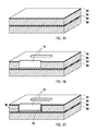
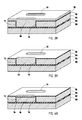
- the sensor element is delineated using a DRIE trench etch, and then is released using a DRIE lateral etch. The lateral etch may be done as a footer etch in a DRIE machine.
Landscapes
- Engineering & Computer Science (AREA)
- Microelectronics & Electronic Packaging (AREA)
- Manufacturing & Machinery (AREA)
- Computer Hardware Design (AREA)
- Pressure Sensors (AREA)
Applications Claiming Priority (1)
| Application Number | Priority Date | Filing Date | Title |
|---|---|---|---|
| US12/011,063 US7645627B2 (en) | 2008-01-24 | 2008-01-24 | Method for manufacturing a sensor device |
Publications (2)
| Publication Number | Publication Date |
|---|---|
| EP2082989A2 true EP2082989A2 (de) | 2009-07-29 |
| EP2082989A3 EP2082989A3 (de) | 2013-10-09 |
Family
ID=40592079
Family Applications (1)
| Application Number | Title | Priority Date | Filing Date |
|---|---|---|---|
| EP09150363.1A Withdrawn EP2082989A3 (de) | 2008-01-24 | 2009-01-12 | Verfahren zur Herstellung eines Sensors |
Country Status (2)
| Country | Link |
|---|---|
| US (1) | US7645627B2 (de) |
| EP (1) | EP2082989A3 (de) |
Families Citing this family (28)
| Publication number | Priority date | Publication date | Assignee | Title |
|---|---|---|---|---|
| US8619378B2 (en) | 2010-11-15 | 2013-12-31 | DigitalOptics Corporation MEMS | Rotational comb drive Z-stage |
| US8768157B2 (en) | 2011-09-28 | 2014-07-01 | DigitalOptics Corporation MEMS | Multiple degree of freedom actuator |
| US8877648B2 (en) * | 2009-03-26 | 2014-11-04 | Semprius, Inc. | Methods of forming printable integrated circuit devices by selective etching to suspend the devices from a handling substrate and devices formed thereby |
| US7998776B1 (en) * | 2010-06-10 | 2011-08-16 | Memsensing Microsystems Technology Co., Ltd. | Methods for manufacturing MEMS sensor and thin film thereof with improved etching process |
| US8605375B2 (en) * | 2010-11-15 | 2013-12-10 | DigitalOptics Corporation MEMS | Mounting flexure contacts |
| US8547627B2 (en) | 2010-11-15 | 2013-10-01 | DigitalOptics Corporation MEMS | Electrical routing |
| US8608393B2 (en) | 2010-11-15 | 2013-12-17 | DigitalOptics Corporation MEMS | Capillary actuator deployment |
| US8884381B2 (en) | 2010-11-15 | 2014-11-11 | DigitalOptics Corporation MEMS | Guard trench |
| US8941192B2 (en) | 2010-11-15 | 2015-01-27 | DigitalOptics Corporation MEMS | MEMS actuator device deployment |
| US9515579B2 (en) | 2010-11-15 | 2016-12-06 | Digitaloptics Corporation | MEMS electrical contact systems and methods |
| US8947797B2 (en) | 2010-11-15 | 2015-02-03 | DigitalOptics Corporation MEMS | Miniature MEMS actuator assemblies |
| US9052567B2 (en) | 2010-11-15 | 2015-06-09 | DigitalOptics Corporation MEMS | Actuator inside of motion control |
| US8637961B2 (en) | 2010-11-15 | 2014-01-28 | DigitalOptics Corporation MEMS | MEMS actuator device |
| US9061883B2 (en) | 2010-11-15 | 2015-06-23 | DigitalOptics Corporation MEMS | Actuator motion control features |
| US8430580B2 (en) | 2010-11-15 | 2013-04-30 | DigitalOptics Corporation MEMS | Rotationally deployed actuators |
| US8803256B2 (en) | 2010-11-15 | 2014-08-12 | DigitalOptics Corporation MEMS | Linearly deployed actuators |
| US9019390B2 (en) | 2011-09-28 | 2015-04-28 | DigitalOptics Corporation MEMS | Optical image stabilization using tangentially actuated MEMS devices |
| US8521017B2 (en) | 2010-11-15 | 2013-08-27 | DigitalOptics Corporation MEMS | MEMS actuator alignment |
| US9352962B2 (en) | 2010-11-15 | 2016-05-31 | DigitalOptics Corporation MEMS | MEMS isolation structures |
| US8604663B2 (en) | 2010-11-15 | 2013-12-10 | DigitalOptics Corporation MEMS | Motion controlled actuator |
| US8616791B2 (en) | 2011-09-28 | 2013-12-31 | DigitalOptics Corporation MEMS | Rotationally deployed actuator devices |
| US8855476B2 (en) | 2011-09-28 | 2014-10-07 | DigitalOptics Corporation MEMS | MEMS-based optical image stabilization |
| DE102013204475A1 (de) | 2013-03-14 | 2014-09-18 | Robert Bosch Gmbh | Herstellungsverfahren für ein mikromechanisches Bauelement und entsprechendes mikromechanisches Bauelement |
| US10167191B2 (en) * | 2017-04-04 | 2019-01-01 | Kionix, Inc. | Method for manufacturing a micro electro-mechanical system |
| US10793427B2 (en) | 2017-04-04 | 2020-10-06 | Kionix, Inc. | Eutectic bonding with AlGe |
| US10053360B1 (en) | 2017-08-11 | 2018-08-21 | Kionix, Inc. | Pseudo SOI process |
| US11313877B2 (en) | 2018-06-19 | 2022-04-26 | Kionix, Inc. | Near-zero power wakeup electro-mechanical system |
| DE102020203576A1 (de) | 2020-03-19 | 2021-09-23 | Robert Bosch Gesellschaft mit beschränkter Haftung | System, insbesondere mikroelektromechanisches System, Verfahren zur Herstellung eines Systems, Verfahren zum Betrieb eines Systems |
Citations (3)
| Publication number | Priority date | Publication date | Assignee | Title |
|---|---|---|---|---|
| US5450751A (en) | 1993-05-04 | 1995-09-19 | General Motors Corporation | Microstructure for vibratory gyroscope |
| US5547093A (en) | 1994-09-14 | 1996-08-20 | Delco Electronics Corporation | Method for forming a micromachine motion sensor |
| US5872313A (en) | 1997-04-07 | 1999-02-16 | Delco Electronics Corporation | Temperature-compensated surface micromachined angular rate sensor |
Family Cites Families (7)
| Publication number | Priority date | Publication date | Assignee | Title |
|---|---|---|---|---|
| US5153143A (en) | 1990-02-26 | 1992-10-06 | Delco Electronics Corporation | Method of manufacturing CMOS integrated circuit with EEPROM |
| US5366916A (en) | 1993-02-04 | 1994-11-22 | Delco Electronics Corporation | Method of making a high voltage implanted channel device for VLSI and ULSI processes |
| US6121552A (en) * | 1997-06-13 | 2000-09-19 | The Regents Of The University Of Caliofornia | Microfabricated high aspect ratio device with an electrical isolation trench |
| US5872034A (en) | 1997-11-03 | 1999-02-16 | Delco Electronics Corporation | EPROM in double poly high density CMOS |
| US6685844B2 (en) * | 2001-02-14 | 2004-02-03 | Delphi Technologies, Inc. | Deep reactive ion etching process and microelectromechanical devices formed thereby |
| DE102004043233B4 (de) | 2003-09-10 | 2014-02-13 | Denso Corporation | Verfahren zum Herstellen eines beweglichen Abschnitts einer Halbleitervorrichtung |
| US7303936B2 (en) * | 2005-04-13 | 2007-12-04 | Delphi Technologies, Inc. | Method for forming anti-stiction bumps on a micro-electro mechanical structure |
-
2008
- 2008-01-24 US US12/011,063 patent/US7645627B2/en active Active
-
2009
- 2009-01-12 EP EP09150363.1A patent/EP2082989A3/de not_active Withdrawn
Patent Citations (3)
| Publication number | Priority date | Publication date | Assignee | Title |
|---|---|---|---|---|
| US5450751A (en) | 1993-05-04 | 1995-09-19 | General Motors Corporation | Microstructure for vibratory gyroscope |
| US5547093A (en) | 1994-09-14 | 1996-08-20 | Delco Electronics Corporation | Method for forming a micromachine motion sensor |
| US5872313A (en) | 1997-04-07 | 1999-02-16 | Delco Electronics Corporation | Temperature-compensated surface micromachined angular rate sensor |
Also Published As
| Publication number | Publication date |
|---|---|
| US7645627B2 (en) | 2010-01-12 |
| US20090191660A1 (en) | 2009-07-30 |
| EP2082989A3 (de) | 2013-10-09 |
Similar Documents
| Publication | Publication Date | Title |
|---|---|---|
| EP2083246B1 (de) | Integrierter Winkelgeschwindigkeitssensor aus Silikon | |
| US7645627B2 (en) | Method for manufacturing a sensor device | |
| EP1116008B1 (de) | Vibrationskreisels und sein herstellungsverfahren | |
| US7270003B2 (en) | BMEMS-type high-sensitivity inertial sensor and manufacturing process thereof | |
| US6845668B2 (en) | Gyroscope | |
| US6988408B2 (en) | Surface/bulk micromachined single-crystalline silicon micro-gyroscope | |
| US9448069B2 (en) | Microelectromechanical bulk acoustic wave devices and methods | |
| US6792804B2 (en) | Sensor for measuring out-of-plane acceleration | |
| US5535902A (en) | Gimballed vibrating wheel gyroscope | |
| US6189381B1 (en) | Angular rate sensor made from a structural wafer of single crystal silicon | |
| EP1212585B1 (de) | Elektrisch entkoppelter mikrogefertigter kreisel | |
| EP0824702B1 (de) | Kardanaufgehängtes gyroskop mit vibrierendem ring, das merkmale zum abbau von spannungen aufweist | |
| US7104129B2 (en) | Vertically integrated MEMS structure with electronics in a hermetically sealed cavity | |
| US7637156B2 (en) | Angular velocity sensor with vibrator having ring portion and electrodes positioned inside and outside the ring portion | |
| EP1677073B1 (de) | Mems-Kreisel mit elektrisch isolierten Bereiche | |
| EP3052901B1 (de) | Trägheits- und drucksensoren auf einem einzelnen chip | |
| JPH05133976A (ja) | 半導体チツプ運動変換器及びその形成方法 | |
| JP6620886B2 (ja) | 微小電気機械デバイス用の電極 | |
| An et al. | Two-input axis angular rate sensor |
Legal Events
| Date | Code | Title | Description |
|---|---|---|---|
| PUAI | Public reference made under article 153(3) epc to a published international application that has entered the european phase |
Free format text: ORIGINAL CODE: 0009012 |
|
| AK | Designated contracting states |
Kind code of ref document: A2 Designated state(s): AT BE BG CH CY CZ DE DK EE ES FI FR GB GR HR HU IE IS IT LI LT LU LV MC MK MT NL NO PL PT RO SE SI SK TR |
|
| AX | Request for extension of the european patent |
Extension state: AL BA RS |
|
| PUAL | Search report despatched |
Free format text: ORIGINAL CODE: 0009013 |
|
| AK | Designated contracting states |
Kind code of ref document: A3 Designated state(s): AT BE BG CH CY CZ DE DK EE ES FI FR GB GR HR HU IE IS IT LI LT LU LV MC MK MT NL NO PL PT RO SE SI SK TR |
|
| AX | Request for extension of the european patent |
Extension state: AL BA RS |
|
| RIC1 | Information provided on ipc code assigned before grant |
Ipc: B81C 1/00 20060101AFI20130904BHEP Ipc: B81B 3/00 20060101ALI20130904BHEP |
|
| AKY | No designation fees paid | ||
| REG | Reference to a national code |
Ref country code: DE Ref legal event code: R108 Effective date: 20140618 |
|
| STAA | Information on the status of an ep patent application or granted ep patent |
Free format text: STATUS: THE APPLICATION IS DEEMED TO BE WITHDRAWN |
|
| 18D | Application deemed to be withdrawn |
Effective date: 20140410 |