EP2080149B1 - System for communicating with a responder - Google Patents
System for communicating with a responder Download PDFInfo
- Publication number
- EP2080149B1 EP2080149B1 EP06783926.6A EP06783926A EP2080149B1 EP 2080149 B1 EP2080149 B1 EP 2080149B1 EP 06783926 A EP06783926 A EP 06783926A EP 2080149 B1 EP2080149 B1 EP 2080149B1
- Authority
- EP
- European Patent Office
- Prior art keywords
- signal
- antenna
- amplifier
- output
- transmitter
- Prior art date
- Legal status (The legal status is an assumption and is not a legal conclusion. Google has not performed a legal analysis and makes no representation as to the accuracy of the status listed.)
- Not-in-force
Links
Images


Classifications
-
- G—PHYSICS
- G06—COMPUTING; CALCULATING OR COUNTING
- G06K—GRAPHICAL DATA READING; PRESENTATION OF DATA; RECORD CARRIERS; HANDLING RECORD CARRIERS
- G06K7/00—Methods or arrangements for sensing record carriers, e.g. for reading patterns
- G06K7/0008—General problems related to the reading of electronic memory record carriers, independent of its reading method, e.g. power transfer
Definitions
- the invention relates to a system according to the preamble of claim 1.
- the invention also relates to a method according to the preamble of claim 29.
- Such a system and method are known from EP-A-0 722 155 .
- the known systems have the drawback that they are sensitive to mistuning of the antenna system, for instance due to environmental factors, such as an electric capacity of a construction, for instance a wall, on which the antenna system is placed.
- the mistuning reduces the efficiency of the system, so that a maximum distance over which the system can communicate with the responder decreases.
- the system is characterized by the characterizing portion of claim 1.
- imaginary component an output impedance at the output of the amplifier, at least at the predetermined transmission frequency, is so high with respect to the impedance of the antenna system that a quality Q and a mistuning of the antenna system with respect to the transmitter are substantially of no importance.
- the efficiency of the transmitter is high when the antenna system is arranged such that the impedance of the antenna system, at least at the predetermined transmission frequency, is substantially free of an imaginary component, since, in that case, the impedance of the antenna system is minimal.
- the system is further provided with a receiver for receiving a second signal from the at least one responder.
- a receiver for receiving a second signal from the at least one responder.
- the antenna system is connected with the receiver.
- This enables a compact design of the system.
- this offers the advantage that an output impedance at the output of the amplifier, at least at the predetermined transmission frequency, is so high that an output voltage of the antenna system upon receiving the second signal from the responder is not, at least hardly influenced by the output impedance of the output of the amplifier connected with the antenna system.
- This is reinforced in that the impedance of the antenna system, at least at the predetermined transmission frequency, is substantially free of the imaginary component.
- a quality Q and a mistuning of the antenna system with respect to the receiver are substantially of no importance therein.
- the system is arranged for transmitting and/or receiving full duplex (FDX) signals.
- FDX full duplex
- the system is arranged for alternately transmitting or receiving half duplex (HDX) signals.
- HDX half duplex
- the system is provided with damping means which can be switched on and off for damping currents through the antenna system, while the system is arranged for switching on the damping means during a period in which the transmitter does not transmit the first signal and in which the receiver receives the second signal and the system is arranged for switching off the damping means during a period in which the transmitter transmits the first signal and in which the receiver does not receive the second signal.
- the quality Q of the antenna system connected with the transmitter is lower than during a period in which the transmitter transmits the first signal.
- the system can communicate with the at least one responder over a distance which is larger than with the system which is not provided with damping means which can be switched on and off.
- the system is arranged for switching on the damping means during a period that the transmitter does not transmit the first signal and before the receiver receives the second signal.
- This offers the advantage that built-up solar energy can be removed from the antenna before the receiver receives the second signal.
- the antenna system is provided with an LC circuit which is arranged such that the impedance of the antenna system, at least at the predetermined transmission frequency, is substantially free of the imaginary component.
- the LC circuit is provided with an antenna which forms an induction of the LC circuit.
- the LC circuit comprises a series capacitor which is connected in series with the antenna, and where, at least at the predetermined transmission frequency, an imaginary component of an impedance of the series capacitor is substantially equal to, and has an opposite sign compared to, an imaginary component of an impedance of the antenna.
- the series capacitor is inserted between the antenna and the output of the amplifier.
- the value of the series capacitor is chosen such that, in use, the emission of signals with a frequency in the range of 0-1000 Hz is prevented, at least reduced, by the antenna. This offers the advantage that, by the antenna system, no, at least fewer high-energy pulses can be formed in the frequency range of 0-1000 Hz, which pulses may, for instance, affect pacemakers. This increases the safety of the system.
- the amplifier is provided with an amplifier stage which, at least at the predetermined transmission frequency, behaves as a voltage source and with a voltage-to-current conversion circuit. This offers the advantage that the amplifiers and/or amplifier stages conventional for this use, which behave as a voltage source at the output, can be used.
- the system is further provided with a transformer, the transformer being inserted between the antenna system and the output of the amplifier.
- a transformer the transformer being inserted between the antenna system and the output of the amplifier.
- the method according to the invention is characterized by the characterizing portion of claim 29.
- EP-A-1610 257 discloses a reader for a transponder. However the reader is not provided with an output which behaves like a current source.
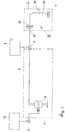
- Fig. 1 shows a schematic representation of a first embodiment of system 1 according to the invention for communicating with at least one responder.
- the system 1 is provided with a transmitter 2, a receiver 4 and an antenna system 6.
- the antenna system 6 is connected with the transmitter 2 and with the receiver 4.
- the transmitter 2 is provided with an amplifier 8.
- the amplifier 8 is provided with an input 10 which is arranged for being connected with a signal source 12 is provided and with an output 14 which is connected with an antenna connection 16 of the antenna system 6.
- an amplifier stage of the amplifier 8 is designed as a current source 18.
- the system shown in Fig. 1 is used as follows.
- a signal source output signal from the signal source 12 is supplied to the input 10 of the amplifier 8 of the transmitter 2.
- the signal source output signal is, for instance, a sinusoidal signal with a predetermined frequency, more in particular a sinusoidal signal composed of at least one digital signal.
- the signal source output signal is amplified, and optionally processed, by the amplifier 8 to an amplifier output signal and supplied to the output 14 of the amplifier 8.
- the output 14 of the amplifier 8 is connected with the antenna system 6, so that the antenna system 6 will transmit a first signal with a predetermined transmission frequency, which first signal corresponds with the amplifier output signal.
- the first signal can be received by a responder. In response to receiving the first signal, the responder will transmit a second signal.
- the second signal is received by the antenna system 6 and causes an antenna output signal corresponding with the received second signal at the antenna connection 16 of the antenna system 6.
- the receiver 4 is connected with the antenna connection 16 and receives the antenna output signal corresponding with the second signal. It therefore holds that the receiver 4 receives the second signal.
- the output 14 of the amplifier 8 behaves like the current source 18.
- an output impedance at the output 14 of the amplifier 8 is so high that, upon receiving the second signal from the responder, an electrical voltage of the antenna output signal at the antenna connection 16 of the antenna system 6 is not, at least hardly, influenced by the output impedance of the output 14 of the amplifier 8 connected with the antenna connection 16 of the antenna system 6. Therefore, the receiver 4 can efficiently and accurately receive the antenna output signal.
- the receiver 4 may, for instance, be designed as an amplitude modulation (AM) receiver or as a frequency shift keyed (FSK) receiver.
- the antenna system 6 is provided with an LC circuit 20 which is arranged such that the impedance of the antenna system 6, at least at the predetermined transmission frequency, is substantially free of an imaginary component.
- the antenna system 6 is provided with an antenna 22, for instance a coil or winding, with the antenna 22 forming an induction 24 of the LC circuit 20.
- the LC circuit 20 comprises a series capacitor 26 which is connected in series with the antenna 22. In Fig. 1 , the series capacitor 26 is inserted between the antenna 22 and the output 14 of the amplifier 8.
- An imaginary component of an impedance of the series capacitor 26, at least at the predetermined transmission frequency, is substantially equal to, and has an opposite sign compared to, an imaginary component of an impedance of the antenna 22, in this example an imaginary component of an impedance of the induction 24.
- the imaginary component of the impedance of the series capacitor 26 compensates for the imaginary component of the impedance of the antenna 22.
- the impedance of the antenna system 6 is therefore, at least at the predetermined transmission frequency, substantially free of the imaginary component.
- the output impedance at the output 14 of the amplifier 8 is high with respect to the impedance of the antenna system 6. Therefore, a mistuning of the antenna system 6 (i.e. a difference in resonance frequency of the antenna system 6 with respect to the transmission frequency, for instance as a result of environmental factors, such as an electrical capacity of a construction, for instance a wall, on which the antenna system 6 is placed) has no or little influence on the efficiency with which the transmitter 2 can transmit the first signal via the antenna system 6, at least less than when the antenna system were connected with the output of an amplifier which behaves like a voltage source, for instance a class D amplifier known per se.
- the system 1 is tolerant to mistuning, which simplifies installation of the system 1.
- the impedance of the antenna system 6 is substantially free of the imaginary component, the impedance of the antenna system 6 is, at least around the predetermined transmission frequency, lower than when the impedance were not substantially free of the imaginary component.
- the efficiency with which the transmitter 2 can transmit the first signal via the antenna system 6 is higher than when the impedance of the antenna system 6 were not substantially free of the imaginary component around the predetermined transmission frequency.
- the efficiency of the transmitter 2 together with the antenna system 6 is therefore higher, and a maximum distance over which the system can communicate with the responder is larger than when the impedance of the antenna system 6 were not substantially free of the imaginary component.
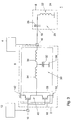
- Fig. 2 shows a schematic representation of a second embodiment of a system 1 according to the invention.
- the amplifier 8 comprises an amplifier stage 28 which behaves like a voltage source.
- the amplifier 8 is further provided with a voltage-to-current conversion circuit 30 which is arranged such that, at least at the predetermined transmission frequency, the output 14 of the amplifier 8 behaves like the current source 18.
- the signal source output signal from the signal source 12 is supplied to the input 10 of the amplifier 8 of the transmitter 2.
- the voltage-to-current conversion circuit 30 comprises a capacitor 32 and two inductions 34, 36.
- a first end of the first induction 34, a first end of the second induction 36 and a first end of the capacitor 32 are interconnected.
- a second end of the first induction 34 is connected with the voltage source 28.
- a second end of the second induction 36 is connected with the output 14 of the amplifier 8.
- a second end of the capacitor 32 is connected with a reference voltage such as mass 38.
- the capacitor 32 and the inductions 34, 36 are dimensioned such that the voltage-to-current conversion circuit 30, at least at the transmission frequency, behaves like the current source 18 at the output 14.
- the voltage-to-current conversion circuit 30 shown in Fig. 2 also behaves like a filter, for instance a low-pass filter for stopping harmonics of the signal source output signal.
- the amplifier may comprise an additional filter.
- the signal source output signal is, for instance, a sinusoidal signal with a predetermined frequency, more in particular a sinusoidal signal composed of at least one digital signal.
- the signal source output signal comprises, for instance, a sinusoidal signal composed of at least one digital signal which is composed such that a number of overtones are not present in the signal source output signal, for instance such that the second to sixth harmonics are not present in the signal source output signal. It is possible to choose the signal source output signal and the voltage-to-current conversion circuit 30 such that the amplifier output signal substantially exclusively consists of the fundamental of the signal source output signal.
- Fig. 3 shows a schematic representation of a third embodiment of the system 1 according to the invention.
- amplifier 8 comprises a class D amplifier 40, which is arranged such that switching takes place between a positive supply voltage 42 and a negative supply voltage 44.
- An output of the class D amplifier 40 is low-Ohm, so that the class D amplifier 40 behaves like the voltage source.
- the output of the class D amplifier 40 is, in this example, connected with the voltage-to-current conversion circuit 30, so that the amplifier 8 behaves like the current source 18 at the output 14, at least at the predetermined transmission frequency.
- the system 1 as shown in Figs. 1-3 may, for instance, be used as a full duplex (FDX) system, where the first signal can be transmitted and the second signal can be received simultaneously, and as a half duplex (HDX) system, where the first signal is transmitted and the second signal is received substantially alternately.
- FDX full duplex
- HDX half duplex
- Fig. 4 shows a schematic representation of a fourth embodiment of a system according to the invention which is particularly suitable for use as a HDX system.
- the system in Fig. 4 is provided with damping means 46 which can be switched on and off for damping currents through the antenna system 6.
- the damping means 46 are switched off during a first period in which the transmitter 2 transmits the first signal and in which the receiver 4 does not receive the second signal.
- the damping means 46 are preferably switched on during a second period in which the receiver 4 receives the second signal and the transmitter 2 does not transmit the first signal.
- the damping means 46 damp the currents through the antenna system, so that the quality Q of the antenna system 6 is lower than when the damping means 46 are switched off.
- the antenna system 6 can receive a signal which is more broadband than when the damping means 46 are switched off. This offers the advantage that an efficiency with which the antenna system 6 receives the second signal and supplies it to the receiver 4 is substantially independent of mistuning of the antenna system with respect to the second signal.
- the quality Q and/or the impedance of the antenna system 6 have substantially no influence on the efficiency with which the receiver 4 receives the second signal.
- the damping means 46 are switched off, so that the impedance of the transmitter 2 is higher than when the damping means 46 are switched on.
- the efficiency with which the transmitter 2 can transmit the first signal via the antenna system 6 is higher than when the damping means 46 are switched on.
- the damping means 46 comprise a damping resistance 48.
- the damping resistance 48 is inserted between the capacitor 32 and mass 38.
- the damping means 46 which can be switched on and off are, in this example, also provided with a switch 50 for switching the damping means 46 on and/or off, in this example by short-circuiting or not short-circuiting the damping resistance 48.
- the damping means 46 may also be switched on in a period that the transmitter 2 does not transmit the first signal, and before the receiver 4 receives the second signal. This offers the possibility that transmission energy present in the antenna system 6 flows away via the damping means 46, in this example via the damping resistance 48, so that the second signal can be detected after the transmission energy present has, at least partly, been reduced.
- Fig. 5 shows a schematic representation of a fifth embodiment of the system 1 according to the invention.
- the system is provided with a transformer 52 which is inserted between the antenna system 6 and the output 14 of the amplifier 8 of the transmitter 2.
- a winding ratio between a primary and a secondary winding of the transformer 52 determines the current through the antenna system 6. This offers the advantage that more design freedom is obtained with respect to the antenna systems to be used.
- transformer 52 in the system 1 as shown in Figs. 2 and 3 . Since not the antenna 22, but the antenna system 6, whose impedance is substantially free of the imaginary component, is damped by the damping means in Fig. 4 , it is also possible to use the transformer 52 in the system as shown in Fig. 4 .
- Using the transformer 52 for instance allows the transmitter 2 to be arranged for supplying 1A of output current to the output 14, while an antenna system 6 as desired, for instance a single-turn antenna, is coupled with the transmitter 2 via the transformer 52.
- the effect of the series capacitor 26 is that no direct current can be fed through the antenna system 6.
- a value of the series capacitor 26 can be chosen such that, in use, emission of signals with a frequency in the range of 0-1000Hz is prevented, at least reduced, by the antenna system. This increases the safety of the system since the frequencies in the range of 0-1000Hz may, for instance, affect pacemakers.
- the impedance of the antenna system 6 can simply be adapted to, for instance, environmental factors, by choosing a different value for the series capacitor 26, for instance by means of a variable capacitor. This may be convenient when a large mistuning is present.
- the tuning of the antenna system 6 may take place according to the following method. During the transmission of the first signal, the value of the series capacitor 26 is varied, while an output voltage at the output 14 of the amplifier is measured. That value of the series capacitor 26 is selected at which the output voltage has the lowest value measured, and at which thus the efficiency of the system 1 is optimal. This is because, at this value, the impedance of the antenna system 6 is the lowest, and therefore substantially free of the imaginary component.
- adjusting the impedance of the antenna system 6 may be carried out manually, but also automatically, for instance by suitable electronic circuit, optionally provided with a microprocessor.
- suitable electronic circuit optionally provided with a microprocessor.
- the system 1 is tolerant to mistuning, so that the risk that the system 1 is not tuned optimally is limited.
- the system according to the invention may for instance, but not exclusively, be used for detecting goods, shoplifting security, identification of persons and/or identification of animals such as for instance cows.
Description
- The invention relates to a system according to the preamble of
claim 1. The invention also relates to a method according to the preamble of claim 29. - Such a system and method are known from
EP-A-0 722 155 . The known systems have the drawback that they are sensitive to mistuning of the antenna system, for instance due to environmental factors, such as an electric capacity of a construction, for instance a wall, on which the antenna system is placed. The mistuning reduces the efficiency of the system, so that a maximum distance over which the system can communicate with the responder decreases. In order to maximize the distance over which the system can communicate with the responder, with the known systems, it is therefore necessary to tune the system to the location where it is installed during installation. This involves extra work, and associated extra risks that the system is not optimally tuned. - It is an object of the invention to improve the system for communicating with the at least one responder.
- To this end, according to the invention, the system is characterized by the characterizing portion of
claim 1. imaginary component. Here, an output impedance at the output of the amplifier, at least at the predetermined transmission frequency, is so high with respect to the impedance of the antenna system that a quality Q and a mistuning of the antenna system with respect to the transmitter are substantially of no importance. In addition, the efficiency of the transmitter is high when the antenna system is arranged such that the impedance of the antenna system, at least at the predetermined transmission frequency, is substantially free of an imaginary component, since, in that case, the impedance of the antenna system is minimal. - Preferably, the system is further provided with a receiver for receiving a second signal from the at least one responder. This offers the advantage that bidirectional communication between the at least one responder and the system is possible.
- Preferably, the antenna system is connected with the receiver. This enables a compact design of the system. In addition, it is thus not necessary to use separate transmitting and receiving antennas. In addition, this offers the advantage that an output impedance at the output of the amplifier, at least at the predetermined transmission frequency, is so high that an output voltage of the antenna system upon receiving the second signal from the responder is not, at least hardly influenced by the output impedance of the output of the amplifier connected with the antenna system. This is reinforced in that the impedance of the antenna system, at least at the predetermined transmission frequency, is substantially free of the imaginary component. A quality Q and a mistuning of the antenna system with respect to the receiver are substantially of no importance therein.
- In a first embodiment, the system is arranged for transmitting and/or receiving full duplex (FDX) signals.
- In a second embodiment, the system is arranged for alternately transmitting or receiving half duplex (HDX) signals.
- Preferably, the system is provided with damping means which can be switched on and off for damping currents through the antenna system, while the system is arranged for switching on the damping means during a period in which the transmitter does not transmit the first signal and in which the receiver receives the second signal and the system is arranged for switching off the damping means during a period in which the transmitter transmits the first signal and in which the receiver does not receive the second signal. As a result, during the period in which the receiver receives the second signal, the quality Q of the antenna system connected with the transmitter is lower than during a period in which the transmitter transmits the first signal. This offers the advantage that, during the period that the transmitter transmits the first signal, the efficiency of the transmitter is high and that, during the period that the receiver receives the second signal, the receiver has a large bandwidth. As a result, the system can communicate with the at least one responder over a distance which is larger than with the system which is not provided with damping means which can be switched on and off.
- Preferably, the system is arranged for switching on the damping means during a period that the transmitter does not transmit the first signal and before the receiver receives the second signal. This offers the advantage that built-up solar energy can be removed from the antenna before the receiver receives the second signal.
- Preferably, the antenna system is provided with an LC circuit which is arranged such that the impedance of the antenna system, at least at the predetermined transmission frequency, is substantially free of the imaginary component. Preferably, the LC circuit is provided with an antenna which forms an induction of the LC circuit. Preferably, the LC circuit comprises a series capacitor which is connected in series with the antenna, and where, at least at the predetermined transmission frequency, an imaginary component of an impedance of the series capacitor is substantially equal to, and has an opposite sign compared to, an imaginary component of an impedance of the antenna. This offers the advantage that the antenna system is provided with a simple structure, where the impedance of the antenna system, at least at the predetermined transmission frequency, is substantially free of the imaginary component.
Preferably, the series capacitor is inserted between the antenna and the output of the amplifier. Preferably, the value of the series capacitor is chosen such that, in use, the emission of signals with a frequency in the range of 0-1000 Hz is prevented, at least reduced, by the antenna. This offers the advantage that, by the antenna system, no, at least fewer high-energy pulses can be formed in the frequency range of 0-1000 Hz, which pulses may, for instance, affect pacemakers. This increases the safety of the system. - In one embodiment, the amplifier is provided with an amplifier stage which, at least at the predetermined transmission frequency, behaves as a voltage source and with a voltage-to-current conversion circuit. This offers the advantage that the amplifiers and/or amplifier stages conventional for this use, which behave as a voltage source at the output, can be used.
- In one embodiment, the system is further provided with a transformer, the transformer being inserted between the antenna system and the output of the amplifier. This offers the advantage that the system is more flexible with respect to choice of antenna than the system where the transformer is not inserted between the antenna system and the output of the amplifier.
- The method according to the invention is characterized by the characterizing portion of claim 29.
-
EP-A-1610 257 discloses a reader for a transponder. However the reader is not provided with an output which behaves like a current source. - In the following, the invention is, by way of example, explained in more detail with reference to the drawing, in which:
-
Fig. 1 shows a schematic representation of a first embodiment of a system according to the invention; -
Fig. 2 shows a schematic representation of a second embodiment of a system according to the invention; -
Fig. 3 shows a schematic representation of a third embodiment of a system according to the invention; -
Fig. 4 shows a schematic representation of a fourth embodiment of a system according to the invention; and -
Fig. 5 shows a schematic representation of a fifth embodiment of a system according to the invention. -
Fig. 1 shows a schematic representation of a first embodiment ofsystem 1 according to the invention for communicating with at least one responder. Thesystem 1 is provided with atransmitter 2, areceiver 4 and anantenna system 6. Theantenna system 6 is connected with thetransmitter 2 and with thereceiver 4. Thetransmitter 2 is provided with anamplifier 8. Theamplifier 8 is provided with aninput 10 which is arranged for being connected with asignal source 12 is provided and with anoutput 14 which is connected with anantenna connection 16 of theantenna system 6. As shown inFig. 1 , an amplifier stage of theamplifier 8 is designed as acurrent source 18. - The system shown in
Fig. 1 is used as follows. In use, to theinput 10 of theamplifier 8 of thetransmitter 2, a signal source output signal from thesignal source 12 is supplied. The signal source output signal is, for instance, a sinusoidal signal with a predetermined frequency, more in particular a sinusoidal signal composed of at least one digital signal. The signal source output signal is amplified, and optionally processed, by theamplifier 8 to an amplifier output signal and supplied to theoutput 14 of theamplifier 8. Theoutput 14 of theamplifier 8 is connected with theantenna system 6, so that theantenna system 6 will transmit a first signal with a predetermined transmission frequency, which first signal corresponds with the amplifier output signal. In use, the first signal can be received by a responder. In response to receiving the first signal, the responder will transmit a second signal. The second signal is received by theantenna system 6 and causes an antenna output signal corresponding with the received second signal at theantenna connection 16 of theantenna system 6. Thereceiver 4 is connected with theantenna connection 16 and receives the antenna output signal corresponding with the second signal. It therefore holds that thereceiver 4 receives the second signal. - The
output 14 of theamplifier 8 behaves like thecurrent source 18. As a result, an output impedance at theoutput 14 of theamplifier 8 is so high that, upon receiving the second signal from the responder, an electrical voltage of the antenna output signal at theantenna connection 16 of theantenna system 6 is not, at least hardly, influenced by the output impedance of theoutput 14 of theamplifier 8 connected with theantenna connection 16 of theantenna system 6. Therefore, thereceiver 4 can efficiently and accurately receive the antenna output signal. Thereceiver 4 may, for instance, be designed as an amplitude modulation (AM) receiver or as a frequency shift keyed (FSK) receiver. - In
Fig. 1 , theantenna system 6 is provided with anLC circuit 20 which is arranged such that the impedance of theantenna system 6, at least at the predetermined transmission frequency, is substantially free of an imaginary component. In the example ofFig. 1 , theantenna system 6 is provided with anantenna 22, for instance a coil or winding, with theantenna 22 forming aninduction 24 of theLC circuit 20. In this example, theLC circuit 20 comprises aseries capacitor 26 which is connected in series with theantenna 22. InFig. 1 , theseries capacitor 26 is inserted between theantenna 22 and theoutput 14 of theamplifier 8. An imaginary component of an impedance of theseries capacitor 26, at least at the predetermined transmission frequency, is substantially equal to, and has an opposite sign compared to, an imaginary component of an impedance of theantenna 22, in this example an imaginary component of an impedance of theinduction 24. The imaginary component of the impedance of theseries capacitor 26 compensates for the imaginary component of the impedance of theantenna 22. The impedance of theantenna system 6 is therefore, at least at the predetermined transmission frequency, substantially free of the imaginary component. - The output impedance at the
output 14 of theamplifier 8 is high with respect to the impedance of theantenna system 6. Therefore, a mistuning of the antenna system 6 (i.e. a difference in resonance frequency of theantenna system 6 with respect to the transmission frequency, for instance as a result of environmental factors, such as an electrical capacity of a construction, for instance a wall, on which theantenna system 6 is placed) has no or little influence on the efficiency with which thetransmitter 2 can transmit the first signal via theantenna system 6, at least less than when the antenna system were connected with the output of an amplifier which behaves like a voltage source, for instance a class D amplifier known per se. As a result, thesystem 1 is tolerant to mistuning, which simplifies installation of thesystem 1. - Since the impedance of the
antenna system 6, at least at the predetermined transmission frequency, is substantially free of the imaginary component, the impedance of theantenna system 6 is, at least around the predetermined transmission frequency, lower than when the impedance were not substantially free of the imaginary component. As a result, the efficiency with which thetransmitter 2 can transmit the first signal via theantenna system 6 is higher than when the impedance of theantenna system 6 were not substantially free of the imaginary component around the predetermined transmission frequency. The efficiency of thetransmitter 2 together with theantenna system 6 is therefore higher, and a maximum distance over which the system can communicate with the responder is larger than when the impedance of theantenna system 6 were not substantially free of the imaginary component. -
Fig. 2 shows a schematic representation of a second embodiment of asystem 1 according to the invention. In the example ofFig. 2 , theamplifier 8 comprises anamplifier stage 28 which behaves like a voltage source. Theamplifier 8 is further provided with a voltage-to-current conversion circuit 30 which is arranged such that, at least at the predetermined transmission frequency, theoutput 14 of theamplifier 8 behaves like thecurrent source 18. In use, to theinput 10 of theamplifier 8 of thetransmitter 2, the signal source output signal from thesignal source 12 is supplied. - In the example of
Fig. 2 , the voltage-to-current conversion circuit 30 comprises acapacitor 32 and twoinductions first induction 34, a first end of thesecond induction 36 and a first end of thecapacitor 32 are interconnected. A second end of thefirst induction 34 is connected with thevoltage source 28. A second end of thesecond induction 36 is connected with theoutput 14 of theamplifier 8. A second end of thecapacitor 32 is connected with a reference voltage such asmass 38. Thecapacitor 32 and theinductions current conversion circuit 30, at least at the transmission frequency, behaves like thecurrent source 18 at theoutput 14. - The voltage-to-
current conversion circuit 30 shown inFig. 2 also behaves like a filter, for instance a low-pass filter for stopping harmonics of the signal source output signal. However, it is also possible for the amplifier to comprise an additional filter. The signal source output signal is, for instance, a sinusoidal signal with a predetermined frequency, more in particular a sinusoidal signal composed of at least one digital signal. The signal source output signal comprises, for instance, a sinusoidal signal composed of at least one digital signal which is composed such that a number of overtones are not present in the signal source output signal, for instance such that the second to sixth harmonics are not present in the signal source output signal. It is possible to choose the signal source output signal and the voltage-to-current conversion circuit 30 such that the amplifier output signal substantially exclusively consists of the fundamental of the signal source output signal. -
Fig. 3 shows a schematic representation of a third embodiment of thesystem 1 according to the invention. In the example ofFig. 3 ,amplifier 8 comprises aclass D amplifier 40, which is arranged such that switching takes place between apositive supply voltage 42 and anegative supply voltage 44. An output of theclass D amplifier 40 is low-Ohm, so that theclass D amplifier 40 behaves like the voltage source. The output of theclass D amplifier 40 is, in this example, connected with the voltage-to-current conversion circuit 30, so that theamplifier 8 behaves like thecurrent source 18 at theoutput 14, at least at the predetermined transmission frequency. - The
system 1 as shown inFigs. 1-3 may, for instance, be used as a full duplex (FDX) system, where the first signal can be transmitted and the second signal can be received simultaneously, and as a half duplex (HDX) system, where the first signal is transmitted and the second signal is received substantially alternately. -
Fig. 4 shows a schematic representation of a fourth embodiment of a system according to the invention which is particularly suitable for use as a HDX system. The system inFig. 4 is provided with dampingmeans 46 which can be switched on and off for damping currents through theantenna system 6. Preferably, the damping means 46 are switched off during a first period in which thetransmitter 2 transmits the first signal and in which thereceiver 4 does not receive the second signal. The damping means 46 are preferably switched on during a second period in which thereceiver 4 receives the second signal and thetransmitter 2 does not transmit the first signal. - During the second period, the damping means 46 damp the currents through the antenna system, so that the quality Q of the
antenna system 6 is lower than when the damping means 46 are switched off. As a result, theantenna system 6 can receive a signal which is more broadband than when the damping means 46 are switched off. This offers the advantage that an efficiency with which theantenna system 6 receives the second signal and supplies it to thereceiver 4 is substantially independent of mistuning of the antenna system with respect to the second signal. The quality Q and/or the impedance of theantenna system 6 have substantially no influence on the efficiency with which thereceiver 4 receives the second signal. - During the first period, the damping means 46 are switched off, so that the impedance of the
transmitter 2 is higher than when the damping means 46 are switched on. As a result, during the first period, the efficiency with which thetransmitter 2 can transmit the first signal via theantenna system 6 is higher than when the damping means 46 are switched on. - In
Fig. 4 , the damping means 46 comprise a dampingresistance 48. In this example, the dampingresistance 48 is inserted between thecapacitor 32 andmass 38. The damping means 46 which can be switched on and off are, in this example, also provided with aswitch 50 for switching the damping means 46 on and/or off, in this example by short-circuiting or not short-circuiting the dampingresistance 48. - The damping means 46 may also be switched on in a period that the
transmitter 2 does not transmit the first signal, and before thereceiver 4 receives the second signal. This offers the possibility that transmission energy present in theantenna system 6 flows away via the damping means 46, in this example via the dampingresistance 48, so that the second signal can be detected after the transmission energy present has, at least partly, been reduced. -
Fig. 5 shows a schematic representation of a fifth embodiment of thesystem 1 according to the invention. InFig. 5 , the system is provided with atransformer 52 which is inserted between theantenna system 6 and theoutput 14 of theamplifier 8 of thetransmitter 2. A winding ratio between a primary and a secondary winding of thetransformer 52 determines the current through theantenna system 6. This offers the advantage that more design freedom is obtained with respect to the antenna systems to be used. - It is also possible to use the
transformer 52 in thesystem 1 as shown inFigs. 2 and3 . Since not theantenna 22, but theantenna system 6, whose impedance is substantially free of the imaginary component, is damped by the damping means inFig. 4 , it is also possible to use thetransformer 52 in the system as shown inFig. 4 . Using thetransformer 52 for instance allows thetransmitter 2 to be arranged for supplying 1A of output current to theoutput 14, while anantenna system 6 as desired, for instance a single-turn antenna, is coupled with thetransmitter 2 via thetransformer 52. - In the examples, the effect of the
series capacitor 26 is that no direct current can be fed through theantenna system 6. A value of theseries capacitor 26 can be chosen such that, in use, emission of signals with a frequency in the range of 0-1000Hz is prevented, at least reduced, by the antenna system. This increases the safety of the system since the frequencies in the range of 0-1000Hz may, for instance, affect pacemakers. - If desired, the impedance of the
antenna system 6 can simply be adapted to, for instance, environmental factors, by choosing a different value for theseries capacitor 26, for instance by means of a variable capacitor. This may be convenient when a large mistuning is present. The tuning of theantenna system 6 may take place according to the following method. During the transmission of the first signal, the value of theseries capacitor 26 is varied, while an output voltage at theoutput 14 of the amplifier is measured. That value of theseries capacitor 26 is selected at which the output voltage has the lowest value measured, and at which thus the efficiency of thesystem 1 is optimal. This is because, at this value, the impedance of theantenna system 6 is the lowest, and therefore substantially free of the imaginary component. It will be clear that adjusting the impedance of theantenna system 6 may be carried out manually, but also automatically, for instance by suitable electronic circuit, optionally provided with a microprocessor. In addition, if theantenna system 6 is tuned, it also holds that thesystem 1 is tolerant to mistuning, so that the risk that thesystem 1 is not tuned optimally is limited. - The system according to the invention may for instance, but not exclusively, be used for detecting goods, shoplifting security, identification of persons and/or identification of animals such as for instance cows.
Claims (29)
- A system (1) for communicating with at least one responder, wherein the system (1) is provided with a transmitter (2) for transmitting at least a first signal with a predetermined transmission frequency and an antenna system (6), wherein the antenna system (6) is connected with the transmitter (2),
wherein the transmitter (2) is provided with an amplifier (8) provided with an input (10) which is arranged for being connected with a signal source (12) and provided with an output (14) which is connected with the antenna system (6),
wherein the amplifier (8) is arranged such that, at least at the predetermined transmission frequency, the output (14) behaves like a current source (18), characterized in that the antenna system (6) is arranged such that an impedance of the antenna system (6), at least at the predetermined transmission frequency, is substantially free of an imaginary component. - A system according to claim 1, wherein the system (1) is further provided with a receiver (4) for receiving a second signal from the at least one responder.
- A system according to claim 2, wherein the antenna system (6) is connected with the receiver (4).
- A system according to any one of claims 2-3, wherein the system (1) is arranged for transmitting and/or receiving full duplex (FDX) signals.
- A system according to any one of claims 2-4, wherein the system (1) is arranged for alternately transmitting or receiving half duplex (HDX) signals.
- A system according to any one of claims 2-5, wherein the receiver (4) comprises an amplitude modulation (AM) receiver.
- A system according to any one of claims 2-6, wherein the receiver (4) comprises a frequency shift keyed (FSK) receiver.
- A system according to claim 5, wherein the system (1) is provided with damping means (46) which can be switched on and off for damping currents through the antenna system (6).
- A system according to claim 8, wherein the system (1) is arranged for switching on the damping means (46) during a period in which the transmitter (2) does not transmit the first signal and in which the receiver (4) receives the second signal.
- A system according to claim 8 or 9, wherein the system (1) is arranged for switching off the damping means (46) during a period in which the transmitter (2) transmits the first signal and in which the receiver (4) does not receive the second signal.
- A system according to claim 10, wherein the system (1) is arranged for switching on the damping means (46) during a period that the transmitter (2) does not transmit the first signal and before the receiver (4) receives the second signal.
- A system according to any one of claims 9-11, wherein the damping means (46) comprise a damping resistance (48), which damping resistance (48) is connected with a reference voltage, such as mass (38).
- A system according to any one of the preceding claims, wherein the antenna system (6) is provided with an LC circuit (20) which is arranged such that the impedance of the antenna system (6), at least at the predetermined transmission frequency, is substantially free of the imaginary component.
- A system according to claim 13, wherein the LC circuit (20) is provided with an antenna (22) which forms an induction (24) of the LC circuit (20).
- A system according to claim 13 or 14, wherein the LC circuit (20) comprises a series capacitor (26) which is connected in series with the antenna (22), and wherein, at least at the predetermined transmission frequency, an imaginary component of an impedance of the series capacitor (26) is substantially equal to, and has an opposite sign to, an imaginary component of an impedance of the antenna (22).
- A system according to claim 15, wherein the series capacitor (26) is inserted between the antenna (22) and the output (14) of the amplifier (8).
- A system according to any one of claims 15 or 16, wherein the value of the series capacitor (26) is chosen such that, in use, the emission of signals with a frequency in the range of 0-1000Hz is prevented, at least reduced, by the antenna (22).
- A system according to any one of the preceding claims, wherein the system (1) is further provided with the signal source (12), which generates a signal source output signal which is supplied to the input (10) of the amplifier (8), wherein the amplifier (8) is arranged such that an amplifier output signal of the amplifier (8) substantially exclusively comprises a fundamental of the signal source output signal.
- A system according to claim 18, wherein the signal source output signal comprises a sinusoidal signal composed of at least one digital signal.
- A system according to claim 18 or 19, wherein the amplifier (8) is provided with a passive low-pass filter (30).
- A system according to any one of claims 18-20, wherein, in use, the amplifier output signal is free of the second to sixth harmonics of the signal source output signal.
- A system according to any one of claims 18-21, wherein, in use, the signal source output signal is free of the second to sixth harmonics of the fundamental.
- A system according to any one of the preceding claims, wherein the amplifier (8) is provided with an amplifier stage (28) which behaves, at least at the predetermined transmission frequency, like a voltage source and with a voltage-to-current conversion circuit (30).
- A system according to claim 23, wherein the amplifier (8) comprises a class D amplifier (40).
- A system according to claim 23 or 24, wherein the voltage-to-current conversion circuit (30) comprises a capacitor (32) and two inductions (34 and 36), wherein a first end of the first induction (34), a first end of the second induction (36) and a first end of the capacitor (32) are interconnected, and
wherein a second end of the first induction (34) is connected with the voltage source (28), and a second end of the second induction (36) is connected with the output (14), and a second end of the capacitor (32) is connected with a reference voltage, such as mass (38). - A system according to any one of the preceding claims, wherein the system (1) is further provided with a transformer (52), wherein the transformer (52) is inserted between the antenna system (6) and the output (14) of the amplifier (8).
- A system according to any one of the preceding claims, wherein the amplifier (8) is arranged for supplying an output current of substantially 1A to the output (14).
- A system according to any one of the preceding claims, wherein the system (1) is further provided with at least one responder, wherein the at least one responder is arranged for receiving the first signal transmitted by the transmitter (2) and transmitting the second signal.
- A method for adapting, for instance to environmental factors, an impedance of an antenna system of a system for communicating with at least one responder,
wherein the system (1) is provided with a transmitter (2) for transmitting at least a first signal with a predetermined transmission frequency and an antenna system (6), wherein the antenna system (6) is connected with the transmitter (2), wherein the transmitter (2) is provided with an amplifier (8) provided with an input (10) which is arranged for being connected with a signal source (12) and provided with an output (14) which is connected with the antenna system (6), and wherein the amplifier (8) is arranged such that, at least at the predetermined transmission frequency, the output (14) behaves like a current source (18), characterized in that
the antenna system (6) is provided with an LC circuit (20) which is arranged such that the impedance of the antenna system (6), at least at the predetermined transmission frequency, is substantially free of an imaginary component, wherein the LC circuit (20) comprises a series capacitor (26) which is connected in series with an antenna (22) of the antenna system (6), and wherein, at least at the predetermined transmission frequency, an imaginary component of an impedance of the series capacitor (26) is substantially equal to, and has an opposite sign to, an imaginary component of an impedance of the antenna (22), comprising- varying the value of the series capacitor (26) during the transmission of a first signal, while an output voltage at the output (14) of the amplifier (8) is measured,- Selecting the value of the series capacitor (26) at which the output voltage has the lowest value measured.
Applications Claiming Priority (1)
| Application Number | Priority Date | Filing Date | Title |
|---|---|---|---|
| PCT/NL2006/000461 WO2008033006A1 (en) | 2006-09-15 | 2006-09-15 | System for communicating with a responder |
Publications (2)
| Publication Number | Publication Date |
|---|---|
| EP2080149A1 EP2080149A1 (en) | 2009-07-22 |
| EP2080149B1 true EP2080149B1 (en) | 2017-06-28 |
Family
ID=38792139
Family Applications (1)
| Application Number | Title | Priority Date | Filing Date |
|---|---|---|---|
| EP06783926.6A Not-in-force EP2080149B1 (en) | 2006-09-15 | 2006-09-15 | System for communicating with a responder |
Country Status (2)
| Country | Link |
|---|---|
| EP (1) | EP2080149B1 (en) |
| WO (1) | WO2008033006A1 (en) |
Families Citing this family (2)
| Publication number | Priority date | Publication date | Assignee | Title |
|---|---|---|---|---|
| GB2465037B (en) | 2009-03-20 | 2012-04-04 | Innovision Res & Tech Plc | Near field rf communications apparatus |
| EP2254074A1 (en) * | 2009-05-20 | 2010-11-24 | Legic Identsystems Ag | Read/write device for non-contact communication |
Family Cites Families (2)
| Publication number | Priority date | Publication date | Assignee | Title |
|---|---|---|---|---|
| JP2698766B2 (en) * | 1995-01-11 | 1998-01-19 | ソニーケミカル株式会社 | Transceiver for non-contact type IC card system |
| EP1610257A1 (en) * | 2004-06-23 | 2005-12-28 | St Microelectronics S.A. | Impedance matching in reader of electromagnetic transponder |
-
2006
- 2006-09-15 WO PCT/NL2006/000461 patent/WO2008033006A1/en active Application Filing
- 2006-09-15 EP EP06783926.6A patent/EP2080149B1/en not_active Not-in-force
Non-Patent Citations (1)
| Title |
|---|
| None * |
Also Published As
| Publication number | Publication date |
|---|---|
| WO2008033006A1 (en) | 2008-03-20 |
| EP2080149A1 (en) | 2009-07-22 |
Similar Documents
| Publication | Publication Date | Title |
|---|---|---|
| EP1927072B1 (en) | Radio frequency identification device systems | |
| CN102378332B (en) | Wireless power transmission apparatus and transmission method thereof | |
| EP2290782B1 (en) | Non-contact electric power feeding apparatus, non-contact electric power receiving apparatus, non-contact electric power feeding method, non-contact electric power receiving method and non-contact electric power feeding system | |
| US20200195306A1 (en) | Multi-use wireless power and data system | |
| EP2413451B1 (en) | Wireless feeding system | |
| EP3175531B1 (en) | Adaptive and multi-transmitter wireless power for robots | |
| US8378524B2 (en) | Non-contact power transmission device | |
| US20110018358A1 (en) | Contactless power supplying communication apparatus, contactless power receiving communication apparatus, power supplying communication controlling method and power receiving communication controlling method | |
| US20150341087A1 (en) | Multi-use wireless power and data system | |
| EP3379734B1 (en) | Nfc reader with remote antenna | |
| EP0829940A2 (en) | Power transmission system, IC card and information communication system using IC card | |
| EP2490343B1 (en) | Near field communication device | |
| WO2016019139A1 (en) | Multi-use wireless power and data system | |
| RU2009113417A (en) | DEVICE TYPE TRANSMITTER AND / OR ELECTRICAL RADIO SIGNALS | |
| CN101743696B (en) | Apparatus and method for the contactless transmission of power and of a data signal | |
| KR20010007102A (en) | Transmitting-receiving device | |
| CN103038979B (en) | ICPT system, parts and method for designing | |
| US20190296587A1 (en) | Tunable/de-tunable wireless power resonator system and related methods | |
| EP2080149B1 (en) | System for communicating with a responder | |
| CN115242368A (en) | Method and device for adjusting phase, near field communication equipment and storage medium | |
| US20210391754A1 (en) | Distributed control adaptive wireless power transfer system | |
| Maulana et al. | Wireless power transfer characterization based on inductive coupling method | |
| CN103502998B (en) | The fetch equipment of contactless communication is carried out with head-end unit | |
| CN100592646C (en) | Remote control data transmitting and receiving apparatus for hearing-aid | |
| KR102193642B1 (en) | Hybrid wireless power transmission device which enables to transmit resonance power signal and induced power signal simultaneously and hybrid wireless power transmission system including the same |
Legal Events
| Date | Code | Title | Description |
|---|---|---|---|
| PUAI | Public reference made under article 153(3) epc to a published international application that has entered the european phase |
Free format text: ORIGINAL CODE: 0009012 |
|
| 17P | Request for examination filed |
Effective date: 20090415 |
|
| AK | Designated contracting states |
Kind code of ref document: A1 Designated state(s): AT BE BG CH CY CZ DE DK EE ES FI FR GB GR HU IE IS IT LI LT LU LV MC NL PL PT RO SE SI SK TR |
|
| 17Q | First examination report despatched |
Effective date: 20090716 |
|
| DAX | Request for extension of the european patent (deleted) | ||
| GRAP | Despatch of communication of intention to grant a patent |
Free format text: ORIGINAL CODE: EPIDOSNIGR1 |
|
| INTG | Intention to grant announced |
Effective date: 20170302 |
|
| GRAS | Grant fee paid |
Free format text: ORIGINAL CODE: EPIDOSNIGR3 |
|
| GRAA | (expected) grant |
Free format text: ORIGINAL CODE: 0009210 |
|
| AK | Designated contracting states |
Kind code of ref document: B1 Designated state(s): AT BE BG CH CY CZ DE DK EE ES FI FR GB GR HU IE IS IT LI LT LU LV MC NL PL PT RO SE SI SK TR |
|
| REG | Reference to a national code |
Ref country code: GB Ref legal event code: FG4D |
|
| REG | Reference to a national code |
Ref country code: CH Ref legal event code: EP |
|
| REG | Reference to a national code |
Ref country code: AT Ref legal event code: REF Ref document number: 905457 Country of ref document: AT Kind code of ref document: T Effective date: 20170715 |
|
| REG | Reference to a national code |
Ref country code: IE Ref legal event code: FG4D |
|
| REG | Reference to a national code |
Ref country code: DE Ref legal event code: R096 Ref document number: 602006052909 Country of ref document: DE |
|
| REG | Reference to a national code |
Ref country code: NL Ref legal event code: FP |
|
| REG | Reference to a national code |
Ref country code: FR Ref legal event code: PLFP Year of fee payment: 12 |
|
| PG25 | Lapsed in a contracting state [announced via postgrant information from national office to epo] |
Ref country code: LT Free format text: LAPSE BECAUSE OF FAILURE TO SUBMIT A TRANSLATION OF THE DESCRIPTION OR TO PAY THE FEE WITHIN THE PRESCRIBED TIME-LIMIT Effective date: 20170628 Ref country code: GR Free format text: LAPSE BECAUSE OF FAILURE TO SUBMIT A TRANSLATION OF THE DESCRIPTION OR TO PAY THE FEE WITHIN THE PRESCRIBED TIME-LIMIT Effective date: 20170929 Ref country code: FI Free format text: LAPSE BECAUSE OF FAILURE TO SUBMIT A TRANSLATION OF THE DESCRIPTION OR TO PAY THE FEE WITHIN THE PRESCRIBED TIME-LIMIT Effective date: 20170628 |
|
| REG | Reference to a national code |
Ref country code: LT Ref legal event code: MG4D |
|
| REG | Reference to a national code |
Ref country code: AT Ref legal event code: MK05 Ref document number: 905457 Country of ref document: AT Kind code of ref document: T Effective date: 20170628 |
|
| PG25 | Lapsed in a contracting state [announced via postgrant information from national office to epo] |
Ref country code: SE Free format text: LAPSE BECAUSE OF FAILURE TO SUBMIT A TRANSLATION OF THE DESCRIPTION OR TO PAY THE FEE WITHIN THE PRESCRIBED TIME-LIMIT Effective date: 20170628 Ref country code: BG Free format text: LAPSE BECAUSE OF FAILURE TO SUBMIT A TRANSLATION OF THE DESCRIPTION OR TO PAY THE FEE WITHIN THE PRESCRIBED TIME-LIMIT Effective date: 20170928 Ref country code: LV Free format text: LAPSE BECAUSE OF FAILURE TO SUBMIT A TRANSLATION OF THE DESCRIPTION OR TO PAY THE FEE WITHIN THE PRESCRIBED TIME-LIMIT Effective date: 20170628 |
|
| PG25 | Lapsed in a contracting state [announced via postgrant information from national office to epo] |
Ref country code: RO Free format text: LAPSE BECAUSE OF FAILURE TO SUBMIT A TRANSLATION OF THE DESCRIPTION OR TO PAY THE FEE WITHIN THE PRESCRIBED TIME-LIMIT Effective date: 20170628 Ref country code: SK Free format text: LAPSE BECAUSE OF FAILURE TO SUBMIT A TRANSLATION OF THE DESCRIPTION OR TO PAY THE FEE WITHIN THE PRESCRIBED TIME-LIMIT Effective date: 20170628 Ref country code: CZ Free format text: LAPSE BECAUSE OF FAILURE TO SUBMIT A TRANSLATION OF THE DESCRIPTION OR TO PAY THE FEE WITHIN THE PRESCRIBED TIME-LIMIT Effective date: 20170628 Ref country code: EE Free format text: LAPSE BECAUSE OF FAILURE TO SUBMIT A TRANSLATION OF THE DESCRIPTION OR TO PAY THE FEE WITHIN THE PRESCRIBED TIME-LIMIT Effective date: 20170628 Ref country code: AT Free format text: LAPSE BECAUSE OF FAILURE TO SUBMIT A TRANSLATION OF THE DESCRIPTION OR TO PAY THE FEE WITHIN THE PRESCRIBED TIME-LIMIT Effective date: 20170628 |
|
| PG25 | Lapsed in a contracting state [announced via postgrant information from national office to epo] |
Ref country code: ES Free format text: LAPSE BECAUSE OF FAILURE TO SUBMIT A TRANSLATION OF THE DESCRIPTION OR TO PAY THE FEE WITHIN THE PRESCRIBED TIME-LIMIT Effective date: 20170628 Ref country code: IT Free format text: LAPSE BECAUSE OF FAILURE TO SUBMIT A TRANSLATION OF THE DESCRIPTION OR TO PAY THE FEE WITHIN THE PRESCRIBED TIME-LIMIT Effective date: 20170628 Ref country code: IS Free format text: LAPSE BECAUSE OF FAILURE TO SUBMIT A TRANSLATION OF THE DESCRIPTION OR TO PAY THE FEE WITHIN THE PRESCRIBED TIME-LIMIT Effective date: 20171028 Ref country code: PL Free format text: LAPSE BECAUSE OF FAILURE TO SUBMIT A TRANSLATION OF THE DESCRIPTION OR TO PAY THE FEE WITHIN THE PRESCRIBED TIME-LIMIT Effective date: 20170628 |
|
| REG | Reference to a national code |
Ref country code: DE Ref legal event code: R097 Ref document number: 602006052909 Country of ref document: DE |
|
| PG25 | Lapsed in a contracting state [announced via postgrant information from national office to epo] |
Ref country code: DK Free format text: LAPSE BECAUSE OF FAILURE TO SUBMIT A TRANSLATION OF THE DESCRIPTION OR TO PAY THE FEE WITHIN THE PRESCRIBED TIME-LIMIT Effective date: 20170628 |
|
| REG | Reference to a national code |
Ref country code: CH Ref legal event code: PL |
|
| PLBE | No opposition filed within time limit |
Free format text: ORIGINAL CODE: 0009261 |
|
| STAA | Information on the status of an ep patent application or granted ep patent |
Free format text: STATUS: NO OPPOSITION FILED WITHIN TIME LIMIT |
|
| PG25 | Lapsed in a contracting state [announced via postgrant information from national office to epo] |
Ref country code: MC Free format text: LAPSE BECAUSE OF FAILURE TO SUBMIT A TRANSLATION OF THE DESCRIPTION OR TO PAY THE FEE WITHIN THE PRESCRIBED TIME-LIMIT Effective date: 20170628 |
|
| 26N | No opposition filed |
Effective date: 20180329 |
|
| REG | Reference to a national code |
Ref country code: IE Ref legal event code: MM4A |
|
| REG | Reference to a national code |
Ref country code: BE Ref legal event code: MM Effective date: 20170930 |
|
| PG25 | Lapsed in a contracting state [announced via postgrant information from national office to epo] |
Ref country code: LU Free format text: LAPSE BECAUSE OF NON-PAYMENT OF DUE FEES Effective date: 20170915 |
|
| PG25 | Lapsed in a contracting state [announced via postgrant information from national office to epo] |
Ref country code: CH Free format text: LAPSE BECAUSE OF NON-PAYMENT OF DUE FEES Effective date: 20170930 Ref country code: IE Free format text: LAPSE BECAUSE OF NON-PAYMENT OF DUE FEES Effective date: 20170915 Ref country code: LI Free format text: LAPSE BECAUSE OF NON-PAYMENT OF DUE FEES Effective date: 20170930 |
|
| PG25 | Lapsed in a contracting state [announced via postgrant information from national office to epo] |
Ref country code: BE Free format text: LAPSE BECAUSE OF NON-PAYMENT OF DUE FEES Effective date: 20170930 Ref country code: SI Free format text: LAPSE BECAUSE OF FAILURE TO SUBMIT A TRANSLATION OF THE DESCRIPTION OR TO PAY THE FEE WITHIN THE PRESCRIBED TIME-LIMIT Effective date: 20170628 |
|
| REG | Reference to a national code |
Ref country code: FR Ref legal event code: PLFP Year of fee payment: 13 |
|
| PG25 | Lapsed in a contracting state [announced via postgrant information from national office to epo] |
Ref country code: HU Free format text: LAPSE BECAUSE OF FAILURE TO SUBMIT A TRANSLATION OF THE DESCRIPTION OR TO PAY THE FEE WITHIN THE PRESCRIBED TIME-LIMIT; INVALID AB INITIO Effective date: 20060915 |
|
| PG25 | Lapsed in a contracting state [announced via postgrant information from national office to epo] |
Ref country code: CY Free format text: LAPSE BECAUSE OF NON-PAYMENT OF DUE FEES Effective date: 20170628 |
|
| PGFP | Annual fee paid to national office [announced via postgrant information from national office to epo] |
Ref country code: FR Payment date: 20190927 Year of fee payment: 14 |
|
| PGFP | Annual fee paid to national office [announced via postgrant information from national office to epo] |
Ref country code: GB Payment date: 20190925 Year of fee payment: 14 |
|
| PG25 | Lapsed in a contracting state [announced via postgrant information from national office to epo] |
Ref country code: TR Free format text: LAPSE BECAUSE OF FAILURE TO SUBMIT A TRANSLATION OF THE DESCRIPTION OR TO PAY THE FEE WITHIN THE PRESCRIBED TIME-LIMIT Effective date: 20170628 |
|
| PG25 | Lapsed in a contracting state [announced via postgrant information from national office to epo] |
Ref country code: PT Free format text: LAPSE BECAUSE OF FAILURE TO SUBMIT A TRANSLATION OF THE DESCRIPTION OR TO PAY THE FEE WITHIN THE PRESCRIBED TIME-LIMIT Effective date: 20170628 |
|
| GBPC | Gb: european patent ceased through non-payment of renewal fee |
Effective date: 20200915 |
|
| PG25 | Lapsed in a contracting state [announced via postgrant information from national office to epo] |
Ref country code: FR Free format text: LAPSE BECAUSE OF NON-PAYMENT OF DUE FEES Effective date: 20200930 |
|
| PG25 | Lapsed in a contracting state [announced via postgrant information from national office to epo] |
Ref country code: GB Free format text: LAPSE BECAUSE OF NON-PAYMENT OF DUE FEES Effective date: 20200915 |
|
| PGFP | Annual fee paid to national office [announced via postgrant information from national office to epo] |
Ref country code: NL Payment date: 20210824 Year of fee payment: 16 |
|
| PGFP | Annual fee paid to national office [announced via postgrant information from national office to epo] |
Ref country code: DE Payment date: 20210920 Year of fee payment: 16 |
|
| REG | Reference to a national code |
Ref country code: DE Ref legal event code: R119 Ref document number: 602006052909 Country of ref document: DE |
|
| REG | Reference to a national code |
Ref country code: NL Ref legal event code: MM Effective date: 20221001 |
|
| PG25 | Lapsed in a contracting state [announced via postgrant information from national office to epo] |
Ref country code: NL Free format text: LAPSE BECAUSE OF NON-PAYMENT OF DUE FEES Effective date: 20221001 |
|
| PG25 | Lapsed in a contracting state [announced via postgrant information from national office to epo] |
Ref country code: DE Free format text: LAPSE BECAUSE OF NON-PAYMENT OF DUE FEES Effective date: 20230401 |