EP2079289A2 - Printed wiring board and printed substrate unit - Google Patents
Printed wiring board and printed substrate unit Download PDFInfo
- Publication number
- EP2079289A2 EP2079289A2 EP08171766A EP08171766A EP2079289A2 EP 2079289 A2 EP2079289 A2 EP 2079289A2 EP 08171766 A EP08171766 A EP 08171766A EP 08171766 A EP08171766 A EP 08171766A EP 2079289 A2 EP2079289 A2 EP 2079289A2
- Authority
- EP
- European Patent Office
- Prior art keywords
- wiring
- glass fiber
- space
- fiber yarns
- wirings
- Prior art date
- Legal status (The legal status is an assumption and is not a legal conclusion. Google has not performed a legal analysis and makes no representation as to the accuracy of the status listed.)
- Withdrawn
Links
Images


Classifications
-
- H—ELECTRICITY
- H05—ELECTRIC TECHNIQUES NOT OTHERWISE PROVIDED FOR
- H05K—PRINTED CIRCUITS; CASINGS OR CONSTRUCTIONAL DETAILS OF ELECTRIC APPARATUS; MANUFACTURE OF ASSEMBLAGES OF ELECTRICAL COMPONENTS
- H05K1/00—Printed circuits
- H05K1/02—Details
- H05K1/03—Use of materials for the substrate
- H05K1/0313—Organic insulating material
- H05K1/0353—Organic insulating material consisting of two or more materials, e.g. two or more polymers, polymer + filler, + reinforcement
- H05K1/0366—Organic insulating material consisting of two or more materials, e.g. two or more polymers, polymer + filler, + reinforcement reinforced, e.g. by fibres, fabrics
-
- H—ELECTRICITY
- H05—ELECTRIC TECHNIQUES NOT OTHERWISE PROVIDED FOR
- H05K—PRINTED CIRCUITS; CASINGS OR CONSTRUCTIONAL DETAILS OF ELECTRIC APPARATUS; MANUFACTURE OF ASSEMBLAGES OF ELECTRICAL COMPONENTS
- H05K1/00—Printed circuits
- H05K1/02—Details
- H05K1/0213—Electrical arrangements not otherwise provided for
- H05K1/0237—High frequency adaptations
-
- H—ELECTRICITY
- H05—ELECTRIC TECHNIQUES NOT OTHERWISE PROVIDED FOR
- H05K—PRINTED CIRCUITS; CASINGS OR CONSTRUCTIONAL DETAILS OF ELECTRIC APPARATUS; MANUFACTURE OF ASSEMBLAGES OF ELECTRICAL COMPONENTS
- H05K2201/00—Indexing scheme relating to printed circuits covered by H05K1/00
- H05K2201/02—Fillers; Particles; Fibers; Reinforcement materials
- H05K2201/0275—Fibers and reinforcement materials
- H05K2201/029—Woven fibrous reinforcement or textile
-
- H—ELECTRICITY
- H05—ELECTRIC TECHNIQUES NOT OTHERWISE PROVIDED FOR
- H05K—PRINTED CIRCUITS; CASINGS OR CONSTRUCTIONAL DETAILS OF ELECTRIC APPARATUS; MANUFACTURE OF ASSEMBLAGES OF ELECTRICAL COMPONENTS
- H05K2201/00—Indexing scheme relating to printed circuits covered by H05K1/00
- H05K2201/09—Shape and layout
- H05K2201/09209—Shape and layout details of conductors
- H05K2201/09218—Conductive traces
- H05K2201/09236—Parallel layout
Definitions
- the present invention relates to a printed wiring board used for, for example, differential signal transmission.
- a relay apparatus is used to construct, for example, a backbone communication network.
- a printed substrate unit is assembled on the relay apparatus.
- a plurality of LSI (large scale integrated circuit) chips are mounted on a front surface of a printed wiring board in the printed substrate unit.
- the LSI chips are connected to each other by, for example, a pair of wiring patterns extending in the printed wiring board.
- the wiring patterns are separated from each other by predetermined spaces. Differential signal transmission is realized between the LSI chips.
- the printed wiring board is composed of resin along with a yarn or cloth such as one made of glass fiber.
- the glass fiber yarn or cloth is impregnated with the resin.
- the glass fiber is woven into a cloth having warps and wefts.
- the wiring patterns described above extend in parallel with, for example, the warps. Predetermined spaces are partitioned between the warps. The spaces are filled with the resin. When, for example, one wiring pattern coincides with a space, i.e. with the resin in a relatively large area, the other wiring pattern coincides with the warps in the relatively large area.
- Patent Document 1 Japanese Laid-open Patent Publication No. 2003-218271 .
- Patent Document 2 Japanese Laid-open Patent Publication No. H10-117048 .
- Patent Document 3 Japanese Laid-open Patent Publication No. 2006-100699 .
- the resin and glass fiber yarn have different dielectric constants.
- characteristic impedance is dispersed between one wiring pattern and the other wiring pattern depending on whether the resin and the glass which coincide with each other have a large area or not.
- a differential signal has a different transmission speed.
- the difference of the transmission speed causes a time lag of a voltage change in an LSI chip on a receiving side. As a result, the signal cannot be accurately transmitted.
- a printed wiring board comprising:
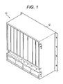
- FIG. 1 is a perspective view schematically showing a structure of a specific example of electronic equipment, i.e. a transmission apparatus 11.
- the transmission apparatus 11 is assembled with, for example, a dense wavelength division multiplexing (DWDM) communication system.
- the transmission apparatus 11 is mounted on, for example, a rack.
- the transmission apparatus 11 has a housing 12.
- a printed substrate unit embodying the present invention, i.e. a mother board is assembled in an accommodation space of the housing 12.
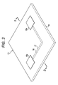
- FIG. 2 schematically shows a structure of the mother board 13 according to the embodiment.
- the mother board 13 has, for example, a large printed wiring board 14.
- a pair of electronic parts i.e. a first LSI (large scale integrated circuit) chip package 15a and a second LSI chip package 15b, for example, is mounted on a front surface of the printed wiring board 14.
- the first and second LSI chip packages 15a, 15b are fixed to the printed wiring board 14 by, for example, a ball grid array (BGA).
- BGA ball grid array
- the first LSI chip package 15a and the second LSI chip package 15b are individually connected electrically by, for example, a first linear wiring pattern 16 and a second linear wiring pattern 17. With this arrangement, differential signal transmission is established between the first LSI chip package 15a and the second LSI chip package 15b based on, for example, a differential voltage.
- the first and second wiring patterns 16, 17 are disposed in parallel with each other in, for example, the printed wiring board 14.
- the first and second wiring patterns 16, 17 are bent at right angles.
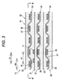
- FIG. 3 schematically shows a structure of the printed wiring board 14 according to a first embodiment.
- the printed wiring board 14 has core resin layers 21 and insulation layers 22 formed on front surfaces and back surfaces of the core resin layers 21.
- the core resin layers 21 and the insulation layers 22 have resin main bodies 23.
- the main bodies 23 are made of, for example, epoxy resin.
- the core resin layers 21 have such a degree of rigidity that they maintain their shapes by themselves.
- the core resin layer 21 and the insulation layers 22 have a thickness of, for example, about 100 ⁇ m to 200 ⁇ m, respectively.
- Glass fiber cloth 24 is embedded in the main bodies 23.
- the glass fiber cloth 24 has a thickness of, for example, about 30 ⁇ m.
- the glass fiber cloth 24 is woven from a plurality of warps 26 and a plurality of wefts 27.
- the plurality of warps 26 are mutually disposed in parallel with each other, and the plurality of wefts 27 are mutually disposed in parallel with each other.
- the warps 26 and wefts 27 are disposed orthogonally to each other.
- the warps 26 are disposed with equal spaces with each other.
- the wefts 27 are disposed with equal spaces with each other.
- the warps 26 and wefts 27 are composed of glass fiber yarns.
- each warp 26 and weft 27 is composed of a bundle of a plurality of glass fibers.
- each warp 26 and weft 27 may be composed of one glass fiber. It is sufficient to impregnate the glass fiber cloth 24 with resin when the core resin layers 21 and the insulation layers 22 described above are formed.
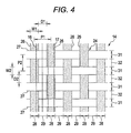
- the width W1 of the warps 26 and the width W2 of the wefts 27 are made the same width.
- the space D1 of warps 26, which are located adjacent to each other, is made the same as the width W1 of the warps 26.
- the space D2 of wefts 27, which are located adjacent to each other, is made the same as the width W2 of the wefts 27.
- the space P1 between the center lines of adjacent warps 26, which extend in parallel with each other is made twice the width W1 and the space D1, respectively.
- the space P2 between the center lines of adjacent wefts 27, which extend in parallel with each other is made twice the width W2 and the space D2, respectively.
- the space P1 is made the same as the space P2.
- the space P1 and the space P2 are made uniform between the core resin layers 21 and the insulation layers 22.
- first regions 28 containing the warps 26 in the printed wiring board 14 The width of the first regions 28 is prescribed by the width W1 of the warps 26.
- Second regions 29 are located adjacent to the first regions 28.
- the second regions 29 are prescribed by the space between adjacent warps 26. That is, the width of the second regions 29 is prescribed by the space D1. Since no warps 26 are disposed in the second regions 29, a relatively large amount of resin is contained in the second regions 29.
- First and second regions 28, 29 are alternately partitioned.
- first regions 31 containing the wefts 27 in the printed wiring board 14 a relatively large amount of glass fibers is contained in first regions 31 containing the wefts 27 in the printed wiring board 14.
- the width of the first regions 31 is prescribed by the width W2 of the wefts 27.
- Second regions 32 are located adjacent to the first regions 31.
- the second regions 32 are prescribed by the space between adjacent wefts 27. That is, the width of the second regions 32 is prescribed by the space D2. Since no wefts 27 are disposed in the second regions 32, a relatively large amount of resin is contained in the second regions 32.
- First regions 31 and second regions 32 are alternately partitioned.
- the first and second wiring patterns 16, 17 described above are formed on a front surface of the core resin layer 21.
- the first and second wiring patterns 16, 17 are formed of a conductive material, for example, copper.
- the width of the first and second wiring patterns 16, 17 is made, for example, about 100 ⁇ m.
- the first wiring pattern 16 and the second wiring pattern 17 extend in parallel with the warps 26. Since the first and second wiring patterns 16, 17 are bent at right angles, they also extend in parallel with the wefts 27.
- the first wiring pattern 16 has a first wiring 34 to a fourth wiring 37.
- the first and second wiring patterns 34, 35 extend in parallel with the warps 26.
- the first LSI chip package 15a is connected to one end of the first wiring 34.
- the length of the first wiring 34 is made the same as the length of the second wiring 35.
- the other end of the second wiring 35 is connected to one end of the third wiring 36.
- the third and fourth wirings 36, 37 extend in parallel with the wefts 27.
- the length of the third wiring 36 is made the same as the length of the fourth wiring 37.
- the second LSI chip package 15b is connected to the other end of the fourth wiring 37.
- the other end of the first wiring 34 and one end of the second wiring 35 are connected by a first connection wiring 38.
- the first connection wiring 38 extends in parallel with the wefts 27. That is, the first connection wiring 38 extends in a direction orthogonal to the warps 26.
- the other end of the third wiring 36 and one end of the fourth wiring 37 are connected by a second connection wiring 39.
- the second connection wiring 39 extends in parallel with the warps 26. That is, the second connection wiring 39 extends in a direction orthogonal to the wefts 27.
- the second wiring pattern 17 has a first wiring 44 to a fourth wiring 47.
- the first and second wirings 44, 45 extend in parallel with the warps 26.
- the first LSI chip package 15a is connected to one end of the first wiring 44.
- the length of the first wiring 44 is set to the same as the length of the second wiring 45.
- the other end of the second wiring 45 is connected to one end of the third wiring 46.
- the third and fourth wirings 46, 47 extend in parallel with the wefts 27.
- the length of the third wiring 46 is made the same as the length of the fourth wiring 47.
- the second LSI chip package 15b is connected to the other end of the fourth wiring 47.
- the other end of the first wiring 44 and one end of the second wiring 45 are connected by a first connection wiring 48.
- the first connection wiring 48 extends in parallel with the wefts 27. That is, the first connection wiring 48 extends in a direction orthogonal to the warps 26.
- the other end of the third wiring 46 and one end of the fourth wiring 47 are connected by a second connection wiring 49.
- the second connection wiring 49 extends in parallel with the warps 26. That is, the second connection wiring 49 extends in a direction orthogonal to the wefts 27.
- the length of the first wiring 16 is made the same as the length of the second wiring 17. Accordingly, it is sufficient to make the lengths of the first and second wirings 34, 35 the same as the lengths of the first and second wirings 44, 45 between the first and second wiring patterns 16, 17. It is sufficient for the first connection wirings 38, 48 to have the same length. Likewise, it is sufficient to make the lengths of the third and fourth wirings 36, 37 the same as the lengths of the third and fourth wirings 46, 47. It is sufficient for the second connection wirings 39, 49 to have the same length.
- the center line of the first wiring 34 is separated from the center line of the second wiring 35 corresponding thereto by a space S1 of (space P1 x 1/2 + space P1 x N).
- N is set to an integer of at least 0 (zero).
- N 0, that is, the space S1 is set to one half the space P1.
- the center line of the third wiring 36 is separated from the center line of the fourth wiring 37 corresponding thereto by a space S2 of (space P2 x 1/2 + space P2 x N).
- N is set to an integer of at least 0 (zero).
- N 0, that is, the space S2 is set to one half the space P2.
- the center line of the first wiring 44 is separated from the center line of the second wiring 45 corresponding thereto by a space S1 of (space P1 x 1/2 + space P1 x N).
- N is set to an integer of at least 0 (zero).
- N 0, that is, the space S1 is set to one half the space P1.
- the center line of the third wiring 46 is separated from the center line of the fourth wiring 47 corresponding thereto by a space S2 of (space P2 x 1/2 + space P2 x N).
- N is set to an integer of at least 0 (zero).
- N 0, that is, the space S2 is set to one half the space P2.
- the space S1 agrees with the space S2.
- the printed wiring board 14 has a pair of the first wirings 34, 44 and a pair of the second wirings 35, 45, i.e. even pairs of wirings which extend in parallel with the warps 26. At the same time, the printed wiring board 14 has a pair of the first connection wirings 38, 48, i.e. odd pairs of connection wirings. Likewise, the printed wiring board 14 has a pair of the third wirings 36, 46 and a pair of the fourth wirings 37, 47, i.e.: even pairs of wirings which extend in parallel with the wefts 27. At the same time, the printed wiring board 14 has a pair of the second connection wirings 39, 49, i.e. odd pairs of connection wirings.
- the ratio of the first wiring 34 (the third wiring 36) disposed in the first region 28 (the first region 31) and the second region 29 (second region 32) is prescribed exactly opposite to the ratio of the second wiring 35 (the fourth wiring 37) disposed in the first region 28 (the first region 31) and the second region 29 (second region 32). Since the first wiring 34 (the third wiring 36) and the second wiring 35 (the fourth wiring 37) have the same length, the ratios of the glass fiber and the resin covered to the first wiring 34 (the third wiring 36) are set exactly opposite to the ratios of the glass fiber and the resin covered to the second wiring 35 (the fourth wiring 37). Accordingly, in the first wiring pattern 16, a dielectric constant is set to the same value.
- the ratio of the first wiring 44 (the third wiring 46) disposed in the first region 28 (the first region 31) and the second region 29 (second region 32) is prescribed exactly opposite to the ratio of the second wiring 45 (the fourth wiring 47) disposed in the first region 28 (the first regions 31) and the second region 29 (second region 32). Since the first wiring 44 (the third wiring 46) and the second wiring 45 (the fourth wiring 47) have the same length, the ratios of the glass fiber and the resin covered to the first wiring 44 (the third wiring 46) are set exactly opposite to the ratios of the glass fiber and the resin covered to the second wiring 45 (the fourth wiring 47). Accordingly, in the second wiring pattern 17, a dielectric constant is set to the same value.
- FIG. 7 schematically shows a structure of a printed wiring board 14a according to a second embodiment.
- the number of wirings and connection wirings increase as compared with that of the printed wiring board 14 described above.
- a first wiring pattern 16 has a first wiring 51 to a fourth wiring 54 extending in parallel with warps 26 and a fifth wiring 55 to an eighth wiring 58 extending in parallel with wefts 27.
- the first wiring 51 is connected to a first LSI chip package 15a.
- the fourth wiring 54 is connected to the fifth wirings 55.
- the eighth wiring 58 is connected to a second LSI chip package 15b.
- the first and second wirings 51, 52, the second and third wirings 52, 53 as well as the third and fourth wirings 53, 54 are connected by a first connection wiring 61 to a third connection wiring 63, respectively.
- the first wiring 61 to the third wiring 63 extend in parallel with the wefts 27.
- the fifth and sixth wirings 55, 56, the sixth and seventh wirings 56, 57 as well as the seventh and eighth wirings 57, 58 are connected by a fourth connection wiring 64 to a sixth connection wiring 66, respectively.
- the fourth wiring 64 to the sixth wiring 66 extend in parallel with the warps 26.
- the sum of the lengths of all the s-th wirings (s is an odd number of at least 1) extending in parallel with the warps 26 is set equal to the sum of the lengths of all the t-th wirings (t is an even number of at least two) extending in parallel with the warps 26. Accordingly, the sum of the lengths of the first and third wirings 51, 53 is set equal to the sum of the lengths of the second and fourth wirings 52, 54.
- the sum of the lengths of all the s-th wirings (s is an odd number of at least 1) extending in parallel with the wefts 27 is set equal to the sum of the lengths of all the t-th wirings (t is an even number of at least two) extending in parallel with the wefts 27. Accordingly, the sum of the lengths of the fifth and seventh wirings 55, 57 is set equal to the sum of the lengths of the sixth and eighth wiring 56, 58.
- the center line of an r-th wiring (r is an integer of at least 1) is separated from the center line of an (r+1)-th wiring by a space S1 of (space P1 x 1/2 + space P1 x N).
- N is set to an integer of at least 0 (zero).
- N 0, that is, the space S1 is set to one half the space P1. That is, all of the space between the center lines of the first and second wirings 51, 52, the space between the center lines of the second and third wirings 52, 53, and the space between the center lines of the third and fourth wirings 53, 54 are set to the space S1.
- the center line of the r-th wiring (r is an integer of at least 1) is separated from the center line of the (r+1)-th wiring by a space S2 of (space P1 x 1/2 + space P1 x N).
- N is set to an integer of at least 0 (zero).
- N 0, that is, the space S2 is set to one half the space P2.
- the space S2 agrees with the space S1. That is, all of the space between the center lines of the fifth and sixth wirings 55, 56, the space between the center lines of the sixth and seventh wirings 56, 57, and the space between the center lines of the seventh and eighth wirings 57, 58 are set to the space S2.
- the second wiring pattern 17 is arranged likewise the first wiring pattern 16.
- the second wiring pattern 17 has a first wiring 71 to a fourth wiring 74 extending in parallel with the warps 26 and a fifth wiring 75 to an eighth wiring 78 extending in parallel with the wefts 27.
- the first wiring 71 is connected to the first LSI chip package 15a.
- the fourth wiring 74 is connected to the fifth wirings 75.
- the eighth wiring 78 is connected to the second LSI chip package 15b.
- the first and second wirings 71, 72, the second and third wirings 72, 73, as well as the third and fourth wirings 73, 74 are connected by a first connection wiring 81 to a third connection wiring 83, respectively.
- the first connection wiring 81 to the third connection wiring 83 extend in parallel with the wefts 27.
- the fifth and sixth wirings 75, 76, the sixth and seventh wirings 76, 77 as well as the seventh and eighth wirings 77, 78 are connected by a fourth connection wiring 84 to a sixth connection wiring 86, respectively.
- the fourth connection wiring 84 to the sixth connection wiring 86 extend in parallel with the warps 26.
- the sum of the lengths of all the s-th wirings (s is an odd number of at least 1) extending in parallel with the warps 26 is set equal to the sum of the lengths of all the t-th wirings (t is an even number of at least two) extending in parallel with the warps 26. Accordingly, the sum of the lengths of the first and third wirings 71, 73 is set equal to the sum of the lengths of the second and fourth wirings 72, 74.
- the sum of the lengths of all the s-th wirings (s is an odd number of at least 1) extending in parallel with the wefts 27 is set equal to the sum of the lengths of all the t-th wirings (t is an even number of at least two) extending in parallel with the wefts 27. Accordingly, the sum of the lengths of the fifth and seventh wirings 75, 77 is set equal to the sum of the lengths of the sixth and eighth wiring 76, 78.
- the center line of the r-th wiring (r is an integer of at least 1) is separated from the center line of the (r+1)-th wiring by the space S1 of (space P1 x 1/2 + space P1 x N).
- N is set to an integer of at least 0 (zero).
- N 0, that is, the space S1 is set to one half the space P1. That is, all of the space between the center lines of the first and second wiring 71, 72, the space between the center lines of the second and third wirings 72, 73, and the space between the center lines of the third and fourth wiring 73, 74 are set to the space S1.
- the center line of the r-th wiring (r is an integer of at least 1) is separated from the center line of the (r+1)-th wiring by the space S2 of (space P2 x 1/2 + space P2 x N).
- N is set to an integer of at least 0 (zero).
- N 0, that is, the space S2 is set to one half the space P2. That is, all of the space between the center lines of the fifth and sixth wirings 75, 76, the space between the center lines of the sixth and seventh wirings 76, 77, and the space between the center lines of the seventh and eighth wirings 77, 78 are set to the space S2.
- the printed wiring board 14a arranged as described above has a pair of the first wirings 51, 71, a pair of the second wirings 52, 72, a pair of the third wiring 53, 73, and a pair of the fourth wiring 54, 74 extending in parallel with the warps 26a, that is, even pairs of the wirings.
- the printed wiring board 14a has a pair of the first connection wiring 61, 81, a pair of the second connection wiring 62, 82, and a pair of the third connection wirings 63, 83, that is, odd pairs of the connection wirings.
- the printed wiring board 14a has a pair of the fourth wiring 54, 74, a pair of the fifth wirings 55, 75, a pair of the sixth wirings 56, 76, and a pair of the fourth wiring 57, 77 extending in parallel with the wefts 27, that is, even pairs of the wirings.
- the printed wiring board 14a has a pair of the fourth connection wiring 64, 84, a pair of the fifth connection wiring 65, 85, and a pair of the sixth connection wirings 66, 86, that is, odd pairs of the connection wirings.
- an arrangement and a structure that are the same as those of the printed wiring board 14 described above are denoted by the same reference numerals.
- the sum of the lengths of the first and third wiring 51, 53 is set equal to the sum of the lengths of the second and fourth wirings 52, 54.
- the ratio of the first wiring 51 (the fifth wiring 55) and the third wiring 53 (the seventh wiring 57) disposed in the first region 28 (the first region 31) and the second region 29 (the second region 32) is prescribed exactly opposite to the ratio of the second wiring 52 (the sixth wiring 56) and the fourth wiring 54 (the eighth wirings 58) disposed in the first region 28 (the first region 31) and the second region 29 (the second region 32).
- the ratios of glass fiber and resin covered to the first wiring 51 (the fifth wiring 55) and the third wiring 53 (the seventh wiring 57) are set exactly opposite to the ratios of glass fiber and resin covered to the second wiring 52 (the sixth wiring 56) and the fourth wiring 54 (eighth wiring 58). Accordingly, in the first wiring pattern 16, a dielectric constant is set to the same value.
- the sum of the lengths of the first and third wirings 71, 73 is set equal to the sum of the lengths of the second and fourth wirings 72, 74.
- the ratio of the first wiring 71 (the fifth wirings 75) and the third wiring 73 (the seventh wiring 77) disposed in the first region 28 (the first regions 31) and the second region 29 (the second region 32) is prescribed exactly opposite to the ratio of the second wiring 72 (sixth wiring 76) and the fourth wiring 74 (the eighth wiring 78) disposed in the first region 28 (the first regions 31) and the second region 29 (the second region 32).
- the ratios of glass fiber and resin covered to the first wiring 71 (the fifth wiring 75) and the third wiring 73 (the seventh wiring 77) are set exactly opposite to the ratios of glass fiber and resin covered to the second wiring 72 (the sixth wiring 76) and the fourth wiring 74 (the eighth wiring 78). Accordingly, in the second wiring pattern 17, a dielectric constant is set to the same value.
- FIG. 8 schematically shows a structure of a printed wiring board 14b according to a third embodiment.
- a first wiring pattern 16 has a first wiring 91 connected to a first LSI chip package 15a at an end and a second wiring 92 connected to the other end of the first wiring 91 at an end and connected to a second LSI chip package 15b at the other end.
- the first wiring 91 and the second wiring 92 are disposed orthogonal to each other. That is, the first wiring 91 extends in parallel with warps 26.
- the second wiring 92 extends in parallel with wefts 27.
- a second wiring pattern 17 has a first wiring 93 connected to the first LSI chip package 15a at an end and a second wiring 94 connected to the other end of the first wiring 93 at an end and connected to the second LSI chip package 15b at the other end.
- the first wiring 93 and the second wiring 94 are disposed orthogonal to each other. That is, the first connection wiring 93 extends in parallel with the warps 26.
- the second wiring 94 extends in parallel with the wefts 27.
- the first wiring 93 extends in parallel with the first wiring 91 extend.
- the second wiring 94 extends in parallel with the second wiring 92.
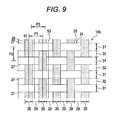
- the space P3 between the center line of the first wiring 91 and the center line of the first wiring 93 is set to an integral multiple of the space P1 described above.
- the space P3 is set one time the space P1, i.e., set to the same as the space P1.
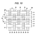
- the space P4 between the center line of the second wiring 92 and the center line of the second wiring 94 is set to an integral multiple of the space P2 described above.
- the space P4 is set one time the space P2, i.e. set to the same as the space P2.
- the width of the first region 28 (the first region 31) may not be set to the same as the width of the second region 29 (the second region 32).
- an arrangement and a structure that are the same as those of the printed wiring board 14 described above are denoted by the same reference numerals.
- the space P3 (the space P4) is set to the same as the space P1 (the space P2).
- the ratio of the first wiring 91 (the second wiring 92) disposed in the first region 28 (the first region 31) and the second region 29 (second region 32) agrees with the ratio of the first wiring 93 (the second wiring 94) disposed in the first region 28 (the first region 31) and the second region 29 (second region 32).
- the dielectric constant of the first wiring pattern 16 agrees with the dielectric constant of the second wiring pattern 17 over the entire lengths thereof.
- the dispersion of characteristic impedance is securely avoided between the first and second wiring patterns 16, 17.
- the disagreement of a transmission speed between the first and second wiring patterns 16, 17 is securely avoided. A differential signal can be correctly transmitted.
Landscapes
- Engineering & Computer Science (AREA)
- Microelectronics & Electronic Packaging (AREA)
- Structure Of Printed Boards (AREA)
- Printing Elements For Providing Electric Connections Between Printed Circuits (AREA)
Abstract
Description
- This application is based upon and claims the benefit of priority of the prior Japanese Patent Application No.
2008-1507, filed on January 8, 2008 - The present invention relates to a printed wiring board used for, for example, differential signal transmission.
- A relay apparatus is used to construct, for example, a backbone communication network. A printed substrate unit is assembled on the relay apparatus. A plurality of LSI (large scale integrated circuit) chips are mounted on a front surface of a printed wiring board in the printed substrate unit. The LSI chips are connected to each other by, for example, a pair of wiring patterns extending in the printed wiring board. The wiring patterns are separated from each other by predetermined spaces. Differential signal transmission is realized between the LSI chips.
- The printed wiring board is composed of resin along with a yarn or cloth such as one made of glass fiber. The glass fiber yarn or cloth is impregnated with the resin. For example, the glass fiber is woven into a cloth having warps and wefts. The wiring patterns described above extend in parallel with, for example, the warps. Predetermined spaces are partitioned between the warps. The spaces are filled with the resin. When, for example, one wiring pattern coincides with a space, i.e. with the resin in a relatively large area, the other wiring pattern coincides with the warps in the relatively large area.
- Patent Document 1: Japanese Laid-open Patent Publication No.
2003-218271 - Patent Document 2: Japanese Laid-open Patent Publication No.
H10-117048 - Patent Document 3: Japanese Laid-open Patent Publication No.
2006-100699 - The resin and glass fiber yarn have different dielectric constants. As a result, characteristic impedance is dispersed between one wiring pattern and the other wiring pattern depending on whether the resin and the glass which coincide with each other have a large area or not. Thus, a differential signal has a different transmission speed. When, for example, a signal is transmitted based on a differential voltage, the difference of the transmission speed causes a time lag of a voltage change in an LSI chip on a receiving side. As a result, the signal cannot be accurately transmitted.
- In view of the above actual circumstances, it is desirable to provide a printed wiring board and a printed substrate unit capable of suppressing an influence of a dielectric constant by a simple structure.
According to a first aspect of the present invention, there is provided a printed wiring board comprising: - a main body made of resin;
- a plurality of yarns which are woven, impregnated with resin of the main body, and disposed in parallel with each other with a predetermined width;
- a pair of first wirings formed on a front surface of the main body and disposed in parallel with the yarns;
- a pair of second wirings formed on a front surface of the main body, disposed in parallel with the yarns, and having the same length as the length of the first wirings corresponding thereto, respectively; and
- a pair of connection wirings for individually connecting the first wiring and the second wiring corresponding thereto while being orthogonal to the yarns,
- Reference is made, by way of example only, to the accompanying drawings in which:
-
FIG. 1 is a perspective view schematically showing a structure of a specific example of electronic equipment, i.e. a transmission apparatus; -
FIG. 2 is a perspective view schematically showing a structure of a printed substrate unit according to the specific example; -
FIG. 3 is a partial vertical sectional view taken along a line 3-3 ofFIG. 2 ; -
FIG. 4 is a sectional view taken along a line 4-4 ofFIG. 3 ; -
FIG. 5 is a view schematically showing a structure of a printed wiring board according to a first embodiment; -
FIG. 6 is a sectional view schematically showing a structure of a wiring pattern; -
FIG. 7 is a view schematically showing a structure of a printed wiring board according to a second embodiment; -
FIG. 8 is a view schematically showing a structure of a printed wiring board according to a third embodiment; -
FIG. 9 is a sectional view schematically showing a structure of a wiring pattern; and -
FIG. 10 is a sectional view schematically showing a structure of a wiring pattern. - In the accompanying drawings, like reference numerals refer to like elements throughout.
- An embodiment will be explained referring to the accompanying drawings.
-
FIG. 1 is a perspective view schematically showing a structure of a specific example of electronic equipment, i.e. atransmission apparatus 11. Thetransmission apparatus 11 is assembled with, for example, a dense wavelength division multiplexing (DWDM) communication system. Thetransmission apparatus 11 is mounted on, for example, a rack. Thetransmission apparatus 11 has ahousing 12. A printed substrate unit embodying the present invention, i.e. a mother board is assembled in an accommodation space of thehousing 12. -
FIG. 2 schematically shows a structure of themother board 13 according to the embodiment. Themother board 13 has, for example, a large printedwiring board 14. A pair of electronic parts, i.e. a first LSI (large scale integrated circuit)chip package 15a and a secondLSI chip package 15b, for example, is mounted on a front surface of the printedwiring board 14. The first and secondLSI chip packages wiring board 14 by, for example, a ball grid array (BGA). - The first
LSI chip package 15a and the secondLSI chip package 15b are individually connected electrically by, for example, a firstlinear wiring pattern 16 and a secondlinear wiring pattern 17. With this arrangement, differential signal transmission is established between the firstLSI chip package 15a and the secondLSI chip package 15b based on, for example, a differential voltage. The first andsecond wiring patterns wiring board 14. The first andsecond wiring patterns -
FIG. 3 schematically shows a structure of the printedwiring board 14 according to a first embodiment. The printedwiring board 14 hascore resin layers 21 andinsulation layers 22 formed on front surfaces and back surfaces of thecore resin layers 21. Thecore resin layers 21 and theinsulation layers 22 have resinmain bodies 23. Themain bodies 23 are made of, for example, epoxy resin. Thecore resin layers 21 have such a degree of rigidity that they maintain their shapes by themselves. Thecore resin layer 21 and theinsulation layers 22 have a thickness of, for example, about 100 µm to 200 µm, respectively. -
Glass fiber cloth 24 is embedded in themain bodies 23. Theglass fiber cloth 24 has a thickness of, for example, about 30 µm. Referring to alsoFIG. 4 , theglass fiber cloth 24 is woven from a plurality ofwarps 26 and a plurality ofwefts 27. The plurality ofwarps 26 are mutually disposed in parallel with each other, and the plurality ofwefts 27 are mutually disposed in parallel with each other. Here, thewarps 26 andwefts 27 are disposed orthogonally to each other. The warps 26 are disposed with equal spaces with each other. Likewise, thewefts 27 are disposed with equal spaces with each other. - The warps 26 and
wefts 27 are composed of glass fiber yarns. Here, eachwarp 26 andweft 27 is composed of a bundle of a plurality of glass fibers. However, eachwarp 26 andweft 27 may be composed of one glass fiber. It is sufficient to impregnate theglass fiber cloth 24 with resin when the core resin layers 21 and the insulation layers 22 described above are formed. - The width W1 of the
warps 26 and the width W2 of thewefts 27 are made the same width. The space D1 ofwarps 26, which are located adjacent to each other, is made the same as the width W1 of thewarps 26. Likewise, the space D2 ofwefts 27, which are located adjacent to each other, is made the same as the width W2 of thewefts 27. Accordingly, the space P1 between the center lines ofadjacent warps 26, which extend in parallel with each other, is made twice the width W1 and the space D1, respectively. Likewise, the space P2 between the center lines ofadjacent wefts 27, which extend in parallel with each other, is made twice the width W2 and the space D2, respectively. The space P1 is made the same as the space P2. The space P1 and the space P2 are made uniform between the core resin layers 21 and the insulation layers 22. - As apparent from
FIG. 4 , a relatively large amount of glass fibers is contained infirst regions 28 containing thewarps 26 in the printedwiring board 14. The width of thefirst regions 28 is prescribed by the width W1 of thewarps 26.Second regions 29 are located adjacent to thefirst regions 28. Thesecond regions 29 are prescribed by the space betweenadjacent warps 26. That is, the width of thesecond regions 29 is prescribed by the space D1. Since nowarps 26 are disposed in thesecond regions 29, a relatively large amount of resin is contained in thesecond regions 29. First andsecond regions - Likewise, a relatively large amount of glass fibers is contained in
first regions 31 containing thewefts 27 in the printedwiring board 14. The width of thefirst regions 31 is prescribed by the width W2 of thewefts 27.Second regions 32 are located adjacent to thefirst regions 31. Thesecond regions 32 are prescribed by the space betweenadjacent wefts 27. That is, the width of thesecond regions 32 is prescribed by the space D2. Since nowefts 27 are disposed in thesecond regions 32, a relatively large amount of resin is contained in thesecond regions 32.First regions 31 andsecond regions 32 are alternately partitioned. - For example, the first and
second wiring patterns core resin layer 21. The first andsecond wiring patterns second wiring patterns first wiring pattern 16 and thesecond wiring pattern 17 extend in parallel with thewarps 26. Since the first andsecond wiring patterns wefts 27. - As shown in
FIG. 5 , thefirst wiring pattern 16 has afirst wiring 34 to afourth wiring 37. The first andsecond wiring patterns warps 26. The firstLSI chip package 15a is connected to one end of thefirst wiring 34. The length of thefirst wiring 34 is made the same as the length of thesecond wiring 35. The other end of thesecond wiring 35 is connected to one end of thethird wiring 36. The third andfourth wirings wefts 27. The length of thethird wiring 36 is made the same as the length of thefourth wiring 37. The secondLSI chip package 15b is connected to the other end of thefourth wiring 37. - The other end of the
first wiring 34 and one end of thesecond wiring 35 are connected by afirst connection wiring 38. Thefirst connection wiring 38 extends in parallel with thewefts 27. That is, thefirst connection wiring 38 extends in a direction orthogonal to thewarps 26. The other end of thethird wiring 36 and one end of thefourth wiring 37 are connected by asecond connection wiring 39. Thesecond connection wiring 39 extends in parallel with thewarps 26. That is, thesecond connection wiring 39 extends in a direction orthogonal to thewefts 27. - Likewise, the
second wiring pattern 17 has afirst wiring 44 to afourth wiring 47. The first andsecond wirings warps 26. The firstLSI chip package 15a is connected to one end of thefirst wiring 44. The length of thefirst wiring 44 is set to the same as the length of thesecond wiring 45. The other end of thesecond wiring 45 is connected to one end of thethird wiring 46. The third andfourth wirings wefts 27. The length of thethird wiring 46 is made the same as the length of thefourth wiring 47. The secondLSI chip package 15b is connected to the other end of thefourth wiring 47. - The other end of the
first wiring 44 and one end of thesecond wiring 45 are connected by afirst connection wiring 48. Thefirst connection wiring 48 extends in parallel with thewefts 27. That is, thefirst connection wiring 48 extends in a direction orthogonal to thewarps 26. The other end of thethird wiring 46 and one end of thefourth wiring 47 are connected by asecond connection wiring 49. Thesecond connection wiring 49 extends in parallel with thewarps 26. That is, thesecond connection wiring 49 extends in a direction orthogonal to thewefts 27. - The length of the
first wiring 16 is made the same as the length of thesecond wiring 17. Accordingly, it is sufficient to make the lengths of the first andsecond wirings second wirings second wiring patterns first connection wirings fourth wirings fourth wirings second connection wirings - In the
first wiring pattern 16, the center line of thefirst wiring 34 is separated from the center line of thesecond wiring 35 corresponding thereto by a space S1 of (space P1 x 1/2 + space P1 x N). N is set to an integer of at least 0 (zero). Here, N = 0, that is, the space S1 is set to one half the space P1. Likewise, the center line of thethird wiring 36 is separated from the center line of thefourth wiring 37 corresponding thereto by a space S2 of (space P2 x 1/2 + space P2 x N). N is set to an integer of at least 0 (zero). Here, N = 0, that is, the space S2 is set to one half the space P2. - In the
second wiring pattern 17, the center line of thefirst wiring 44 is separated from the center line of thesecond wiring 45 corresponding thereto by a space S1 of (space P1 x 1/2 + space P1 x N). N is set to an integer of at least 0 (zero). Here, N = 0, that is, the space S1 is set to one half the space P1. Likewise, the center line of thethird wiring 46 is separated from the center line of thefourth wiring 47 corresponding thereto by a space S2 of (space P2 x 1/2 + space P2 x N). N is set to an integer of at least 0 (zero). Here, N = 0, that is, the space S2 is set to one half the space P2. Here, the space S1 agrees with the space S2. - The printed
wiring board 14 has a pair of thefirst wirings second wirings warps 26. At the same time, the printedwiring board 14 has a pair of thefirst connection wirings wiring board 14 has a pair of thethird wirings fourth wirings wefts 27. At the same time, the printedwiring board 14 has a pair of thesecond connection wirings - As shown in
FIG. 6 , in thefirst wiring pattern 16, the ratio of the first wiring 34 (the third wiring 36) disposed in the first region 28 (the first region 31) and the second region 29 (second region 32) is prescribed exactly opposite to the ratio of the second wiring 35 (the fourth wiring 37) disposed in the first region 28 (the first region 31) and the second region 29 (second region 32). Since the first wiring 34 (the third wiring 36) and the second wiring 35 (the fourth wiring 37) have the same length, the ratios of the glass fiber and the resin covered to the first wiring 34 (the third wiring 36) are set exactly opposite to the ratios of the glass fiber and the resin covered to the second wiring 35 (the fourth wiring 37). Accordingly, in thefirst wiring pattern 16, a dielectric constant is set to the same value. - Likewise, in the
second wiring pattern 17, the ratio of the first wiring 44 (the third wiring 46) disposed in the first region 28 (the first region 31) and the second region 29 (second region 32) is prescribed exactly opposite to the ratio of the second wiring 45 (the fourth wiring 47) disposed in the first region 28 (the first regions 31) and the second region 29 (second region 32). Since the first wiring 44 (the third wiring 46) and the second wiring 45 (the fourth wiring 47) have the same length, the ratios of the glass fiber and the resin covered to the first wiring 44 (the third wiring 46) are set exactly opposite to the ratios of the glass fiber and the resin covered to the second wiring 45 (the fourth wiring 47). Accordingly, in thesecond wiring pattern 17, a dielectric constant is set to the same value. - In the
mother board 13 as described above, even if the first andsecond wiring patterns main body 23, an influence due to the difference between the dielectric constant of the glass fiber and the dielectric constant of the resin is cancelled in the first andsecond wiring patterns second wiring patterns second wiring patterns -
FIG. 7 schematically shows a structure of a printedwiring board 14a according to a second embodiment. In the printedwiring board 14a, the number of wirings and connection wirings increase as compared with that of the printedwiring board 14 described above. Afirst wiring pattern 16 has afirst wiring 51 to afourth wiring 54 extending in parallel withwarps 26 and a fifth wiring 55 to aneighth wiring 58 extending in parallel withwefts 27. Thefirst wiring 51 is connected to a firstLSI chip package 15a. Thefourth wiring 54 is connected to the fifth wirings 55. Theeighth wiring 58 is connected to a secondLSI chip package 15b. - The first and
second wirings third wirings fourth wirings first connection wiring 61 to athird connection wiring 63, respectively. Thefirst wiring 61 to thethird wiring 63 extend in parallel with thewefts 27. In contrast, the fifth andsixth wirings 55, 56, the sixth andseventh wirings eighth wirings fourth connection wiring 64 to asixth connection wiring 66, respectively. Thefourth wiring 64 to thesixth wiring 66 extend in parallel with thewarps 26. - The sum of the lengths of all the s-th wirings (s is an odd number of at least 1) extending in parallel with the
warps 26 is set equal to the sum of the lengths of all the t-th wirings (t is an even number of at least two) extending in parallel with thewarps 26. Accordingly, the sum of the lengths of the first andthird wirings fourth wirings wefts 27 is set equal to the sum of the lengths of all the t-th wirings (t is an even number of at least two) extending in parallel with thewefts 27. Accordingly, the sum of the lengths of the fifth andseventh wirings 55, 57 is set equal to the sum of the lengths of the sixth andeighth wiring - The center line of an r-th wiring (r is an integer of at least 1) is separated from the center line of an (r+1)-th wiring by a space S1 of (
space P1 x 1/2 + space P1 x N). N is set to an integer of at least 0 (zero). Here, N = 0, that is, the space S1 is set to one half the space P1. That is, all of the space between the center lines of the first andsecond wirings third wirings fourth wirings - Likewise, the center line of the r-th wiring (r is an integer of at least 1) is separated from the center line of the (r+1)-th wiring by a space S2 of (
space P1 x 1/2 + space P1 x N). N is set to an integer of at least 0 (zero). Here, N = 0, that is, the space S2 is set to one half the space P2. Here, the space S2 agrees with the space S1. That is, all of the space between the center lines of the fifth andsixth wirings 55, 56, the space between the center lines of the sixth andseventh wirings eighth wirings - In contrast, the
second wiring pattern 17 is arranged likewise thefirst wiring pattern 16. Thesecond wiring pattern 17 has afirst wiring 71 to afourth wiring 74 extending in parallel with thewarps 26 and afifth wiring 75 to aneighth wiring 78 extending in parallel with thewefts 27. Thefirst wiring 71 is connected to the firstLSI chip package 15a. Thefourth wiring 74 is connected to thefifth wirings 75. Theeighth wiring 78 is connected to the secondLSI chip package 15b. - The first and
second wirings third wirings fourth wirings first connection wiring 81 to athird connection wiring 83, respectively. Thefirst connection wiring 81 to thethird connection wiring 83 extend in parallel with thewefts 27. In contrast, the fifth andsixth wirings seventh wirings eighth wirings fourth connection wiring 84 to asixth connection wiring 86, respectively. Thefourth connection wiring 84 to thesixth connection wiring 86 extend in parallel with thewarps 26. - The sum of the lengths of all the s-th wirings (s is an odd number of at least 1) extending in parallel with the
warps 26 is set equal to the sum of the lengths of all the t-th wirings (t is an even number of at least two) extending in parallel with thewarps 26. Accordingly, the sum of the lengths of the first andthird wirings fourth wirings wefts 27 is set equal to the sum of the lengths of all the t-th wirings (t is an even number of at least two) extending in parallel with thewefts 27. Accordingly, the sum of the lengths of the fifth andseventh wirings eighth wiring - The center line of the r-th wiring (r is an integer of at least 1) is separated from the center line of the (r+1)-th wiring by the space S1 of (
space P1 x 1/2 + space P1 x N). N is set to an integer of at least 0 (zero). Here, N = 0, that is, the space S1 is set to one half the space P1. That is, all of the space between the center lines of the first andsecond wiring third wirings fourth wiring - Likewise, the center line of the r-th wiring (r is an integer of at least 1) is separated from the center line of the (r+1)-th wiring by the space S2 of (
space P2 x 1/2 + space P2 x N). N is set to an integer of at least 0 (zero). Here, N = 0, that is, the space S2 is set to one half the space P2. That is, all of the space between the center lines of the fifth andsixth wirings seventh wirings eighth wirings - The printed
wiring board 14a arranged as described above has a pair of thefirst wirings second wirings third wiring fourth wiring wiring board 14a has a pair of thefirst connection wiring second connection wiring wiring board 14a has a pair of thefourth wiring fifth wirings 55, 75, a pair of thesixth wirings fourth wiring wefts 27, that is, even pairs of the wirings. At the same time, the printedwiring board 14a has a pair of thefourth connection wiring fifth connection wiring wiring board 14 described above are denoted by the same reference numerals. - In the
first wiring pattern 16, the sum of the lengths of the first andthird wiring fourth wirings first wiring pattern 16, the ratio of the first wiring 51 (the fifth wiring 55) and the third wiring 53 (the seventh wiring 57) disposed in the first region 28 (the first region 31) and the second region 29 (the second region 32) is prescribed exactly opposite to the ratio of the second wiring 52 (the sixth wiring 56) and the fourth wiring 54 (the eighth wirings 58) disposed in the first region 28 (the first region 31) and the second region 29 (the second region 32). The ratios of glass fiber and resin covered to the first wiring 51 (the fifth wiring 55) and the third wiring 53 (the seventh wiring 57) are set exactly opposite to the ratios of glass fiber and resin covered to the second wiring 52 (the sixth wiring 56) and the fourth wiring 54 (eighth wiring 58). Accordingly, in thefirst wiring pattern 16, a dielectric constant is set to the same value. - Likewise, in the
second wiring pattern 17, the sum of the lengths of the first andthird wirings fourth wirings second wiring pattern 17, the ratio of the first wiring 71 (the fifth wirings 75) and the third wiring 73 (the seventh wiring 77) disposed in the first region 28 (the first regions 31) and the second region 29 (the second region 32) is prescribed exactly opposite to the ratio of the second wiring 72 (sixth wiring 76) and the fourth wiring 74 (the eighth wiring 78) disposed in the first region 28 (the first regions 31) and the second region 29 (the second region 32). The ratios of glass fiber and resin covered to the first wiring 71 (the fifth wiring 75) and the third wiring 73 (the seventh wiring 77) are set exactly opposite to the ratios of glass fiber and resin covered to the second wiring 72 (the sixth wiring 76) and the fourth wiring 74 (the eighth wiring 78). Accordingly, in thesecond wiring pattern 17, a dielectric constant is set to the same value. - In the printed
wiring board 14a as described above, even if the first andsecond wiring patterns main body 23, the influence due to the difference between the dielectric constant of the glass fiber and the dielectric constant of the resin is cancelled in the first andsecond wiring patterns second wiring patterns second wiring patterns -
FIG. 8 schematically shows a structure of a printedwiring board 14b according to a third embodiment. In the printedwiring board 14b, afirst wiring pattern 16 has afirst wiring 91 connected to a firstLSI chip package 15a at an end and asecond wiring 92 connected to the other end of thefirst wiring 91 at an end and connected to a secondLSI chip package 15b at the other end. Thefirst wiring 91 and thesecond wiring 92 are disposed orthogonal to each other. That is, thefirst wiring 91 extends in parallel withwarps 26. Thesecond wiring 92 extends in parallel withwefts 27. - Likewise, a
second wiring pattern 17 has afirst wiring 93 connected to the firstLSI chip package 15a at an end and asecond wiring 94 connected to the other end of thefirst wiring 93 at an end and connected to the secondLSI chip package 15b at the other end. Thefirst wiring 93 and thesecond wiring 94 are disposed orthogonal to each other. That is, thefirst connection wiring 93 extends in parallel with thewarps 26. Thesecond wiring 94 extends in parallel with thewefts 27. Thefirst wiring 93 extends in parallel with thefirst wiring 91 extend. Thesecond wiring 94 extends in parallel with thesecond wiring 92. - As shown in
FIG. 9 , the space P3 between the center line of thefirst wiring 91 and the center line of thefirst wiring 93 is set to an integral multiple of the space P1 described above. Here, the space P3 is set one time the space P1, i.e., set to the same as the space P1. Likewise, as shown inFIG. 10 , the space P4 between the center line of thesecond wiring 92 and the center line of thesecond wiring 94 is set to an integral multiple of the space P2 described above. Here, the space P4 is set one time the space P2, i.e. set to the same as the space P2. Note that in the printedwiring board 14b, the width of the first region 28 (the first region 31) may not be set to the same as the width of the second region 29 (the second region 32). In addition to the above-mentioned, an arrangement and a structure that are the same as those of the printedwiring board 14 described above are denoted by the same reference numerals. - In the printed
wiring board 14b described above, the space P3 (the space P4) is set to the same as the space P1 (the space P2). As a result, even if the first andsecond wiring patterns main body 23, the ratio of the first wiring 91 (the second wiring 92) disposed in the first region 28 (the first region 31) and the second region 29 (second region 32) agrees with the ratio of the first wiring 93 (the second wiring 94) disposed in the first region 28 (the first region 31) and the second region 29 (second region 32). As a result, the dielectric constant of thefirst wiring pattern 16 agrees with the dielectric constant of thesecond wiring pattern 17 over the entire lengths thereof. The dispersion of characteristic impedance is securely avoided between the first andsecond wiring patterns second wiring patterns - Although a few preferred embodiments of the present invention have been shown and described, it would be appreciated by those skilled in the art that changes may be made in these embodiments without departing from the principles of the invention, the scope of which is defined in the claims.
Claims (6)
- A printed wiring board comprising:a main body made of resin;a plurality of glass fiber yarns which are woven, impregnated with resin of the main body, and disposed in parallel with each other with a predetermined width;a pair of first wirings formed on a front surface of the main body and disposed in parallel with the glass fiber yarns;a pair of second wirings formed on a front surface of the main body, disposed in parallel with the glass fiber yarns, and having the same length as the length of the first wirings corresponding thereto, respectively; anda pair of connection wirings for individually connecting the first wiring and the second wiring corresponding thereto while being orthogonal to the glass fiber yarns,wherein the glass fiber yarns adjacent to each other are separated at the same space as the width of the glass fiber yarns; and the center line of the first wiring and the center line of the second wiring corresponding thereto are separated at a space of (space between the center lines of the adjacent glass fiber yarns x 1/2 + space between the center lines of the adjacent glass fiber yarns x N (N is an integer of at least 0 (zero)).
- A printed substrate unit comprising:a main body made of resin;a plurality of glass fiber yarns which are woven, impregnated with resin of the main body, and disposed in parallel with each other with a predetermined width;a pair of first wirings formed on a front surface of the main body and disposed in parallel with the glass fiber yarns;a pair of second wirings formed on a front surface of the main body, extending in parallel with the glass fiber yarns, and having the same length as the length of the first wirings corresponding thereto, respectively;a pair of connection wirings for individually connecting the first wiring and the second wiring corresponding thereto while being orthogonal to the glass fiber yarns; and a pair of electronic parts connected to each other by the first wirings, the connection wirings, and the second wirings,wherein the glass fiber yarns adjacent to each other are separated at the same space as the width of the glass fiber yarns; and the center line of the first wiring and the center line of the second wiring corresponding thereto are separated at a space of (space between the center lines of the adjacent glass fiber yarns x 1/2 + space between the center lines of the adjacent glass fiber yarns x N (N is an integer of at least 0 (zero)).
- A printed wiring board comprising:a main body made of resin;a plurality of glass fiber yarns which are woven, impregnated with resin of the main body, and disposed in parallel with each other with a predetermined width;each one pair of first to m-th wirings (m is an even number of at least two) formed on a front surface of the main body and extending in parallel with the glass fiber yarns; andeach one pair of first to p-th connection wirings (p is an odd number of at least 1) formed on a front surface of the main body for connecting an n-th wiring and an (n + 1)-th wiring (n is an integer of at least one) corresponding thereto individually while being orthogonal to the glass fiber yarns,wherein the glass fiber yarns adjacent to each other are separated at the same space as the width of the glass fiber yarns,the center line of an r-th wiring (r is an integer of at least 1) and the center line of an (r+1)-th wiring corresponding thereto are separated at a space of (space between the center lines of the adjacent glass fiber yarns x 1/2 + space between the center lines of the adjacent glass fiber yarns x N (N is an integer of at least 0 (zero)), andthe sum of the lengths of all the s-th wirings (s is an odd number of at least 1) is equal to the sum of the lengths of all the t-th wirings (t is an even number of at least two).
- A printed substrate unit comprising:a main body made of resin;a plurality of glass fiber yarns which are woven, impregnated with resin of the main body, and disposed in parallel with each other with a predetermined width;each one pair of first to m-th wirings (m is an even number of at least two) formed on a front surface of the main body and disposed in parallel with the glass fiber yarns; andeach one pair of first to p-th connection wirings (p is an odd number of at least 1) formed on a front surface of the main body for individually connecting an n-th wiring and an (n + 1)-th wiring (n is an integer of at least one) corresponding thereto while being orthogonal to the glass fiber yarns; and a pair of electronic parts connected to each other by a first to m-th wirings and a first to p-th connection wirings,wherein the glass fiber yarns adjacent to each other are separated at the same space as the width of the glass fiber yarns; the center line of an r-th wiring (r is an integer of at least 1) and the center line of an (r+1)-th wiring corresponding thereto are separated at a space of (space between the center lines of the adjacent glass fiber yarns x 1/2 + space between the center lines of the adjacent glass fiber yarns x N (N is an integer of at least 0 (zero)), andthe sum of the lengths of all the s-th wirings (s is an odd number of at least 1) is equal to the sum of the lengths of all the t-th wirings (t is an even number of at least two).
- A printed wiring board comprising:a main body made of resin;a plurality of glass fiber yarns which are woven, impregnated with resin of the main body, and extending in parallel with each other; anda pair of wiring patterns extending in parallel with the glass fiber yarns and prescribing a center line at a space that is an integral multiple of the space between the center lines of the glass fiber yarns.
- A printed substrate unit comprising:a main body made of resin;a plurality of glass fiber yarns which are woven, impregnated with resin of the main body, and extending in parallel with each other;a pair of wiring patterns extending in parallel with the glass fiber yarns and prescribing a center line at a space that is an integral multiple of the space between the center lines of the glass fiber yarns; anda pair of electronic parts connected to each other by the wiring patterns.
Applications Claiming Priority (1)
| Application Number | Priority Date | Filing Date | Title |
|---|---|---|---|
| JP2008001507A JP2009164416A (en) | 2008-01-08 | 2008-01-08 | Printed wiring board and printed circuit board unit |
Publications (2)
| Publication Number | Publication Date |
|---|---|
| EP2079289A2 true EP2079289A2 (en) | 2009-07-15 |
| EP2079289A3 EP2079289A3 (en) | 2010-05-19 |
Family
ID=40529230
Family Applications (1)
| Application Number | Title | Priority Date | Filing Date |
|---|---|---|---|
| EP08171766A Withdrawn EP2079289A3 (en) | 2008-01-08 | 2008-12-16 | Printed wiring board and printed substrate unit |
Country Status (3)
| Country | Link |
|---|---|
| US (1) | US20090173525A1 (en) |
| EP (1) | EP2079289A3 (en) |
| JP (1) | JP2009164416A (en) |
Cited By (1)
| Publication number | Priority date | Publication date | Assignee | Title |
|---|---|---|---|---|
| EP2373130A1 (en) * | 2010-03-29 | 2011-10-05 | Fujitsu Limited | Printed wiring board manufacturing method and printed wiring board |
Families Citing this family (9)
| Publication number | Priority date | Publication date | Assignee | Title |
|---|---|---|---|---|
| JP5476906B2 (en) * | 2009-10-05 | 2014-04-23 | 富士通株式会社 | Wiring board manufacturing method and wiring board design method |
| US8237058B2 (en) * | 2010-05-06 | 2012-08-07 | Oracle America, Inc. | Printed circuit board with low propagation skew between signal traces |
| JP5471870B2 (en) * | 2010-06-17 | 2014-04-16 | 富士通株式会社 | Wiring board |
| JP6019657B2 (en) | 2012-03-26 | 2016-11-02 | 富士通株式会社 | Design support program, design support method, design support apparatus, and manufacturing method |
| JP6205721B2 (en) * | 2012-12-28 | 2017-10-04 | 富士通株式会社 | Multilayer circuit board and electronic device |
| JP2015088627A (en) * | 2013-10-31 | 2015-05-07 | 京セラサーキットソリューションズ株式会社 | Wiring board |
| CN105704931B (en) * | 2014-11-28 | 2021-01-22 | 中兴通讯股份有限公司 | Wiring method of differential signal line and PCB |
| JP2016115753A (en) * | 2014-12-12 | 2016-06-23 | 富士通株式会社 | Print circuit board and electronic device |
| WO2016117320A1 (en) * | 2015-01-21 | 2016-07-28 | 日本電気株式会社 | Wiring board and method for designing same |
Citations (4)
| Publication number | Priority date | Publication date | Assignee | Title |
|---|---|---|---|---|
| JPH10117048A (en) | 1996-10-09 | 1998-05-06 | Tec Corp | Printed circuit board |
| JP2003218271A (en) | 2002-01-25 | 2003-07-31 | Sony Corp | High frequency module substrate and high frequency module |
| JP2006100699A (en) | 2004-09-30 | 2006-04-13 | Toshiba Corp | Printed wiring board, information processing apparatus, and printed wiring board manufacturing method |
| JP2008001507A (en) | 2006-06-26 | 2008-01-10 | Hitachi Building Systems Co Ltd | Exterior lighting curing method for renewal of passenger conveyor |
Family Cites Families (7)
| Publication number | Priority date | Publication date | Assignee | Title |
|---|---|---|---|---|
| US3878316A (en) * | 1970-07-08 | 1975-04-15 | Gaylord L Groff | Laminate comprising non-woven fibrous backing |
| US4103102A (en) * | 1976-07-01 | 1978-07-25 | Bell Telephone Laboratories, Incorporated | Reinforced flexible printed wiring board |
| US7043706B2 (en) * | 2003-03-11 | 2006-05-09 | Intel Corporation | Conductor trace design to reduce common mode cross-talk and timing skew |
| US7022919B2 (en) * | 2003-06-30 | 2006-04-04 | Intel Corporation | Printed circuit board trace routing method |
| US7843057B2 (en) * | 2005-11-17 | 2010-11-30 | Intel Corporation | Method of making a fiber reinforced printed circuit board panel and a fiber reinforced panel made according to the method |
| US7427719B2 (en) * | 2006-03-21 | 2008-09-23 | Intel Corporation | Shifted segment layout for differential signal traces to mitigate bundle weave effect |
| CN101494948B (en) * | 2008-01-24 | 2012-07-18 | 鸿富锦精密工业(深圳)有限公司 | Circuit board and its design method |
-
2008
- 2008-01-08 JP JP2008001507A patent/JP2009164416A/en not_active Withdrawn
- 2008-12-16 EP EP08171766A patent/EP2079289A3/en not_active Withdrawn
- 2008-12-18 US US12/338,433 patent/US20090173525A1/en not_active Abandoned
Patent Citations (4)
| Publication number | Priority date | Publication date | Assignee | Title |
|---|---|---|---|---|
| JPH10117048A (en) | 1996-10-09 | 1998-05-06 | Tec Corp | Printed circuit board |
| JP2003218271A (en) | 2002-01-25 | 2003-07-31 | Sony Corp | High frequency module substrate and high frequency module |
| JP2006100699A (en) | 2004-09-30 | 2006-04-13 | Toshiba Corp | Printed wiring board, information processing apparatus, and printed wiring board manufacturing method |
| JP2008001507A (en) | 2006-06-26 | 2008-01-10 | Hitachi Building Systems Co Ltd | Exterior lighting curing method for renewal of passenger conveyor |
Cited By (2)
| Publication number | Priority date | Publication date | Assignee | Title |
|---|---|---|---|---|
| EP2373130A1 (en) * | 2010-03-29 | 2011-10-05 | Fujitsu Limited | Printed wiring board manufacturing method and printed wiring board |
| US8631568B2 (en) | 2010-03-29 | 2014-01-21 | Fujitsu Limited | Printed wiring board manufacturing method |
Also Published As
| Publication number | Publication date |
|---|---|
| EP2079289A3 (en) | 2010-05-19 |
| US20090173525A1 (en) | 2009-07-09 |
| JP2009164416A (en) | 2009-07-23 |
Similar Documents
| Publication | Publication Date | Title |
|---|---|---|
| EP2079289A2 (en) | Printed wiring board and printed substrate unit | |
| JP3808521B2 (en) | Fiber optic ribbons and arrays woven into smart skin arrays and their packaging | |
| CN106337237B (en) | Woven signal routing substrate for wearable electronic devices | |
| CN105704931B (en) | Wiring method of differential signal line and PCB | |
| EP0506298B1 (en) | Smart skin array woven fiber optic ribbon and arrays and packaging thereof | |
| US20080176471A1 (en) | Glass cloth wiring substrate | |
| US8054643B2 (en) | Semiconductor module, wiring board, and wiring method | |
| JP2009164174A (en) | Printed wiring board and printed circuit board unit | |
| US10881001B2 (en) | Micro conductive thread interconnect component to make an interconnect between conductive threads in fabrics to PCB, FPC, and rigid-flex circuits | |
| JP6508219B2 (en) | Wiring board and design method thereof | |
| CN101494948B (en) | Circuit board and its design method | |
| US7056571B2 (en) | Wiring board and its production process | |
| JP6394420B2 (en) | Cable connection structure and cable connector including the same | |
| US8985863B2 (en) | Method to reorder (shuffle) optical cable waveguide layers | |
| JP2009073946A (en) | Insulating substrate, wiring board and multilayer board | |
| KR101355733B1 (en) | Printed circuit board, method of manufacturing the same, and electronic apparatus | |
| US5379193A (en) | Parallel processor structure and package | |
| US9603275B2 (en) | Blackplane board and wiring method of backplane board | |
| US9049794B2 (en) | Wiring substrate and method for manufacturing the wiring substrate | |
| US20190357350A1 (en) | Wiring board and method for manufacturing same | |
| US11596054B2 (en) | Method of producing printed circuit boards with routing conductors and dielectric strands | |
| US12289827B2 (en) | Printed board and electronic device | |
| Muth et al. | Signal propagation and multiplexing challenges in electronic textiles | |
| CN117479421A (en) | High-frequency high-speed prepreg, copper-clad plate and circuit board and manufacturing method | |
| JP2022186154A (en) | Rigid insulating substrate and circuit substrate |
Legal Events
| Date | Code | Title | Description |
|---|---|---|---|
| PUAI | Public reference made under article 153(3) epc to a published international application that has entered the european phase |
Free format text: ORIGINAL CODE: 0009012 |
|
| AK | Designated contracting states |
Kind code of ref document: A2 Designated state(s): AT BE BG CH CY CZ DE DK EE ES FI FR GB GR HR HU IE IS IT LI LT LU LV MC MT NL NO PL PT RO SE SI SK TR |
|
| AX | Request for extension of the european patent |
Extension state: AL BA MK RS |
|
| PUAL | Search report despatched |
Free format text: ORIGINAL CODE: 0009013 |
|
| AK | Designated contracting states |
Kind code of ref document: A3 Designated state(s): AT BE BG CH CY CZ DE DK EE ES FI FR GB GR HR HU IE IS IT LI LT LU LV MC MT NL NO PL PT RO SE SI SK TR |
|
| AX | Request for extension of the european patent |
Extension state: AL BA MK RS |
|
| AKY | No designation fees paid | ||
| REG | Reference to a national code |
Ref country code: DE Ref legal event code: 8566 |
|
| STAA | Information on the status of an ep patent application or granted ep patent |
Free format text: STATUS: THE APPLICATION IS DEEMED TO BE WITHDRAWN |
|
| 18D | Application deemed to be withdrawn |
Effective date: 20101120 |