EP2075858A1 - Organic light emitting device - Google Patents
Organic light emitting device Download PDFInfo
- Publication number
- EP2075858A1 EP2075858A1 EP20080254128 EP08254128A EP2075858A1 EP 2075858 A1 EP2075858 A1 EP 2075858A1 EP 20080254128 EP20080254128 EP 20080254128 EP 08254128 A EP08254128 A EP 08254128A EP 2075858 A1 EP2075858 A1 EP 2075858A1
- Authority
- EP
- European Patent Office
- Prior art keywords
- light emitting
- organic light
- emitting device
- layer
- electrode
- Prior art date
- Legal status (The legal status is an assumption and is not a legal conclusion. Google has not performed a legal analysis and makes no representation as to the accuracy of the status listed.)
- Granted
Links
Images

Classifications
-
- H—ELECTRICITY
- H05—ELECTRIC TECHNIQUES NOT OTHERWISE PROVIDED FOR
- H05B—ELECTRIC HEATING; ELECTRIC LIGHT SOURCES NOT OTHERWISE PROVIDED FOR; CIRCUIT ARRANGEMENTS FOR ELECTRIC LIGHT SOURCES, IN GENERAL
- H05B33/00—Electroluminescent light sources
- H05B33/12—Light sources with substantially two-dimensional [2D] radiating surfaces
- H05B33/20—Light sources with substantially two-dimensional [2D] radiating surfaces characterised by the chemical or physical composition or the arrangement of the material in which the electroluminescent material is embedded
-
- H—ELECTRICITY
- H10—SEMICONDUCTOR DEVICES; ELECTRIC SOLID-STATE DEVICES NOT OTHERWISE PROVIDED FOR
- H10K—ORGANIC ELECTRIC SOLID-STATE DEVICES
- H10K50/00—Organic light-emitting devices
- H10K50/10—OLEDs or polymer light-emitting diodes [PLED]
- H10K50/14—Carrier transporting layers
-
- C—CHEMISTRY; METALLURGY
- C09—DYES; PAINTS; POLISHES; NATURAL RESINS; ADHESIVES; COMPOSITIONS NOT OTHERWISE PROVIDED FOR; APPLICATIONS OF MATERIALS NOT OTHERWISE PROVIDED FOR
- C09K—MATERIALS FOR MISCELLANEOUS APPLICATIONS, NOT PROVIDED FOR ELSEWHERE
- C09K11/00—Luminescent materials, e.g. electroluminescent or chemiluminescent
- C09K11/06—Luminescent materials, e.g. electroluminescent or chemiluminescent containing organic luminescent materials
-
- H—ELECTRICITY
- H10—SEMICONDUCTOR DEVICES; ELECTRIC SOLID-STATE DEVICES NOT OTHERWISE PROVIDED FOR
- H10K—ORGANIC ELECTRIC SOLID-STATE DEVICES
- H10K50/00—Organic light-emitting devices
-
- H—ELECTRICITY
- H10—SEMICONDUCTOR DEVICES; ELECTRIC SOLID-STATE DEVICES NOT OTHERWISE PROVIDED FOR
- H10K—ORGANIC ELECTRIC SOLID-STATE DEVICES
- H10K50/00—Organic light-emitting devices
- H10K50/10—OLEDs or polymer light-emitting diodes [PLED]
- H10K50/14—Carrier transporting layers
- H10K50/15—Hole transporting layers
- H10K50/155—Hole transporting layers comprising dopants
-
- H—ELECTRICITY
- H10—SEMICONDUCTOR DEVICES; ELECTRIC SOLID-STATE DEVICES NOT OTHERWISE PROVIDED FOR
- H10K—ORGANIC ELECTRIC SOLID-STATE DEVICES
- H10K50/00—Organic light-emitting devices
- H10K50/10—OLEDs or polymer light-emitting diodes [PLED]
- H10K50/14—Carrier transporting layers
- H10K50/16—Electron transporting layers
- H10K50/165—Electron transporting layers comprising dopants
-
- H—ELECTRICITY
- H10—SEMICONDUCTOR DEVICES; ELECTRIC SOLID-STATE DEVICES NOT OTHERWISE PROVIDED FOR
- H10K—ORGANIC ELECTRIC SOLID-STATE DEVICES
- H10K50/00—Organic light-emitting devices
- H10K50/10—OLEDs or polymer light-emitting diodes [PLED]
- H10K50/17—Carrier injection layers
-
- H—ELECTRICITY
- H10—SEMICONDUCTOR DEVICES; ELECTRIC SOLID-STATE DEVICES NOT OTHERWISE PROVIDED FOR
- H10K—ORGANIC ELECTRIC SOLID-STATE DEVICES
- H10K50/00—Organic light-emitting devices
- H10K50/10—OLEDs or polymer light-emitting diodes [PLED]
- H10K50/17—Carrier injection layers
- H10K50/171—Electron injection layers
-
- Y—GENERAL TAGGING OF NEW TECHNOLOGICAL DEVELOPMENTS; GENERAL TAGGING OF CROSS-SECTIONAL TECHNOLOGIES SPANNING OVER SEVERAL SECTIONS OF THE IPC; TECHNICAL SUBJECTS COVERED BY FORMER USPC CROSS-REFERENCE ART COLLECTIONS [XRACs] AND DIGESTS
- Y10—TECHNICAL SUBJECTS COVERED BY FORMER USPC
- Y10T—TECHNICAL SUBJECTS COVERED BY FORMER US CLASSIFICATION
- Y10T428/00—Stock material or miscellaneous articles
- Y10T428/31504—Composite [nonstructural laminate]
Definitions
- the present invention relates to an organic light emitting device, and more particularly, to an organic light emitting device with improved driving voltage, light emitting efficiency, lifetime, and the like by using a novel hole injecting material and a novel electron transporting material.
- the present invention contributes to development of a high image quality organic light emitting device, and provides an organic light emitting device with reduced power consumption and improved lifetime.
- Organic light emitting devices are devices in which, when a current is supplied to an organic layer interposed between two electrodes, electrons and holes combine in the organic layer to emit light. Such organic light emitting devices can be formed as light-weight and thin information display devices having a high image quality, quick response time, and wide viewing angles. These features have led to rapid development of organic light emitting display device technology. Currently, organic light emitting devices are widely used in mobile phones and other information display devices.
- organic light emitting devices Due to such rapid development of organic light emitting devices, competition with other information display devices such as TFT-LCDs is inevitable in terms of academic and industrial technology. In addition, conventional organic light emitting devices are limited in terms of the amount of efficiency and lifetime improvements and power consumption reduction that is possible. The need to improve efficiency and reduce power consumption is an important factor interfering with quantitative and qualitative growth of organic light emitting devices, and it is desirable that this issue be resolved.
- the present invention provides an organic light emitting device having reduced power consumption, improved driving voltage, light emitting efficiency and lifetime by introducing a novel hole injecting material and a novel electron transporting material.
- an organic light emitting device comprising: a first electrode; a second electrode; an emissive layer disposed between the first electrode and the second electrode; a first hole injection layer disposed between the first electrode and the emissive layer; and a first electron transport layer disposed between the emissive layer and the second electrode
- the first hole injection layer comprises a hole injecting material and a first compound comprising an element selected from the group consisting of Mo, Li, Na, K, Rb, Cs, Be, Mg, Ca, Sr, Ba, ytterbium and B and an element selected from the group consisting of O, F, S, Cl, Se, Br, and I
- the first electron transport layer comprises an electron transporting material and a second compound, which is represented by Formula 1 below: ⁇ Formula 1> X a Y b wherein:
- the organic light emitting device further comprises a second hole injection layer in addition to the first hole injection layer.
- the organic light emitting device further comprises a second electron transport layer in addition to the first electron transport layer.
- the first aspect of the present invention provides a first hole injection layer including a hole injecting material and a first compound comprising an element selected from the group consisting of Mo, Li, Na, K, Rb, Cs, Be, Mg, Ca, Sr, Ba, B, and ytterbium and an element selected from the group consisting of O, F, S, Cl, Se, Br, and I.
- the first aspect of the present invention provides a first electron transport layer including a second compound, which is a metal-containing compound represented by Formula 1 below, and an electron transporting material.
- the first compound may be a molybdenum oxide, a magnesium fluoride, a cesium fluoride, a boron oxide, a lithium oxide, an ytterbium oxide, or the like.
- the first compound may be prepared using various methods that are known to one of ordinary skill in the art.
- the hole injecting material can be any known organic hole injecting material such as, for example, copper phthalocyanine, 1 ,3,5-tricarbazolylbenzene, 4,4'-biscarbazolylbiphenyl, polyvinylcarbazole, m-biscarbazolylphenyl, 4,4'-biscarbazolyl-2,2'-dimethylbiphenyl, 4,4',4"-tri(N-carbazolyl)triphenylamine (TCTA), 4,4',4"-tris(3-methylphenylamino)triphenylamine (m-MTDATA), 1,3,5-tri(2-carbazolylphenyl)benzene, 1,3,5-tris(2-carbazolyl-5-methoxyphenyl)benzene, bis(4-carbazolylphenyl)silane, N,N'-bis(3-methylphenyl)-N,N'-diphenyl-[1,1-bipheny
- the mixing ratio of the first compound to the hole injecting material may be in the range of 1:1 to 3:1. Although other embodiments of the invention have mixing ratios falling outside this range, it will often be preferred.
- the mixing ratio of the first compound to the hole injecting material is less than 1:1, that is, when the amount of the first compound is relatively lower and the amount of the hole injecting material is relatively higher, the injection voltage may be increased.
- the mixing ratio of the first compound to the hole transporting material is greater than 3:1, that is, when the amount of the first compound is relatively much higher and the amount of the hole injecting material is relatively lower, the hole injection layer may have insulating properties.
- the metallic properties of an element selected from the group consisting of Mo, Li, Na, K, Rb, Cs, Be, Mg, Ca, Sr, Ba, and B can be utilized such that the contact resistance at the electrode interface is decreased, and thus, interface properties of electrodes using a semiconducting compound, ohmic contact, can be obtained.
- An organic light emitting device having such structures described above, according to the present invention can reduce the hole injection barrier, and also can reduce the contact resistance at the interface of the electrode, and thus, when the organic light emitting device operates, the organic light emitting device can have a longer lifetime.
- An organic light emitting device further includes a second hole injection layer.
- the second hole injection layer may be formed of a conventional organic hole injecting material without including the first compound.
- the second hole injection layer may comprise at least one hole injecting material selected from the group consisting of copper phthalocyanine, 1,3,5-tricarbazolylbenzene, 4,4'-biscarbazolylbiphenyl, polyvinylcarbazole, m-biscarbazolylphenyl, 4,4'-biscarbazolyl-2,2'-dimethylbiphenyl, 4,4',4"-tri(N-carbazolyl)triphenylamine (TCTA), 4,4',4"-tris(3-methylphenylamino)triphenylamine (m-MTDATA),1,3,5-tri(2-carbazolylphenyl)benzene, 1,3,5-tris(2-carbazolyl-5-methoxyphenyl)benzene, bis(4-carbazolylphenyl)silane, N,N'-bis(3-
- the organic light emitting device of the present invention includes a hole injection layer having a two-layered structure, that is, a first hole injection layer and a second hole injection layer, the effects described above are even more pronounced.
- the organic light emitting device includes the second hole injection layer, barriers when holes are transferred to a hole transport layer from the first hole injection layer can be reduced.
- the thickness ratio of the first hole injection layer to the second hole injection layer may be in the range of 1:99 to 1:9. Although other embodiments of the invention have mixing ratios falling outside this range, it will often be preferred.
- the thickness ratio of the first hole injection layer to the second hole injection layer is less than 1:99, that is, when the thickness of the first hole injection layer is much thinner with respect to the second hole injection layer, the effect of a reduction in hole injection barrier may be reduced.
- the thickness ratio of the first hole injection layer to the second hole injection layer is greater than 1:9, that is, when the thickness of the first hole injection layer is not much thinner with respect to the second hole injection layer, hole transporting ability to an electric field may be reduced.
- the organic light emitting device further includes a first electron transport layer that comprises an electron transporting material and a second compound, which is a metal-containing compound represented by Formula 1, above.
- X may be Li, Cs, Na, Ba, or Mg
- Y may be fluoride, quinolate, acetoacetate, chloride, or bromide.
- the electron transport layer comprises a halide element
- the properties of electron injection from an electrode vary depending on the strength of electronegativity of the halide.
- the second compound may be a metal halide containing a halogen atom, such as lithium fluoride, a metal complex material such as lithium quinolate, lithium acetoacetate, and the like, or mixtures thereof.
- the compound may comprise at least one selected from the group consisting of lithium quinolate, sodium quinolate, lithium acetoacetate, magnesium acetoacetate, lithium fluoride, cesium fluoride, sodium fluoride, and lithium oxide.
- the first electron transporting material may comprise an electron transporting material having an electron mobility of 10 -8 cm 2 /V•s or more in an electric field of 800 to 1000 V/cm.
- the first electron transporting material of the first electron transport layer may be Alq 3 , Bebq 2 , Znq, or the like
- the amount of the second compound, (the metal-containing compound of Formula 1) may be in the range of 30 to 50 parts by weight based on 100 parts by weight of the electron transporting material.
- an electron injection layer may be omitted without lowering the ability of electron injection in OLEDs.
- the organic light emitting device may further include a second electron transport layer in addition to the first electron transport layer described above.
- the second electron transport layer comprises a second electron transporting material, which may be the same as or different from the first electron transporting material.
- the organic light emitting device according to the present invention may include a first electron transport layer comprising the second compound (the metal-containing compound of Formula 1) and a first electron transporting material, and a second electron transport layer comprising a second electron transporting material and not containing the second compound.
- the second electron transporting material may be the same as the first electron transporting material in terms of electron injection barriers and electron mobility.
- the second electron transporting material may have an electron mobility of 10 -8 cm 2 /V•s or more in an electric field of 800 to 1000 V/cm, or more specifically, 10 -4 to 10 -8 cm 2 /V•s, in an electric field of 800 to 1000 V/cm, and may be Alq 3 , Bebq 2 , Znq, or the like.
- the organic light emitting device includes the two-layered electron transport layer as described above, a much more systematic electron injection is possible compared with the case where an organic light emitting device includes a single-layered electron transport layer. Thus, power consumption may be significantly reduced due to voltage reduction.
- a separate electron injection layer may be omitted from the organic light emitting device described herein.
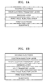
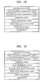
- FIGS. 1A through 1F are schematic cross-sectional views illustrating structures of organic light emitting devices according to embodiments of the present invention.
- the organic light emitting device may have a structure of an anode, a hole injection layer (HIL), a hole transport layer (HTL), an emissive layer (EML), an electron transport layer (ETL), an electron injection layer (EIL), and a cathode.
- HIL hole injection layer
- HTL hole transport layer
- EML emissive layer
- ETL electron transport layer
- EIL electron injection layer
- cathode a cathode
- the organic light emitting device may further include additional layers, such as one-layered or two-layered intermediate layers, if desired, and may have other structures or layers in addition to the layers shown in FIGS. 1A - 1F .
- a material for a first electrode material is coated onto a substrate to form a first electrode (typically, an anode).
- the substrate may comprise a substrate material typically used in conventional organic light emitting devices.
- the substrate may be a glass substrate or a plastic substrate having good transparency, surface smoothness, manageability and waterproofness.
- the material for the anode can be a transparent and highly conductive material, such as ITO, IZO, SnO 2 , ZnO, or the like.
- HIL hole injection layer
- vacuum deposition conditions may vary according to the compound used to form the HIL, and the desired structure and thermal properties of the HIL to be formed. In general, however, the vacuum deposition may be performed at a deposition temperature of 50-500°C, a pressure of 10 -8 -10 -3 torr, and a deposition speed of 0.01-100 ⁇ /sec.
- the thickness of the HIL may be in the range of 10 ⁇ to 5 ⁇ m.
- a hole transport layer is formed on the HIL using a hole transporting material.
- the HTL may be formed by vacuum deposition, spin coating, casting, LB deposition, or the like; for example, the HTL may be formed on the HIL by vacuum deposition such that a uniform film may be easily formed and so that pin holes are not easily formed.
- the deposition conditions may vary according to the compound used to form the HTL. In general, however, the deposition conditions may be similar to those used for the formation of the HIL.
- the hole transporting material is not particularly limited, and may be N,N'-bis(3-methylphenyl)-N,N'-diphenyl-[1,1-biphenyl]-4,4'-diamine (TPD), N,N'-di(naphthalene-1-yl)-N,N'-diphenyl benzidine ( ⁇ -NPD), or the like.
- an emissive layer is formed on the HTL.
- the EML can be formed by vacuum deposition, spin coating, casting, LB deposition, or the like.
- the material for forming the EML is not particularly limited.
- the material for forming the EML may be a blue emitting material such as oxadiazole dimer dyes (such as Bis-DAPOXP), spiro compounds (such as Spiro-DPVBi, Spiro-6P), triarylamine compounds, bis(styryl)amine compounds (such as DPVBi, DSA), 4,4'-bis(9-ethyl-3-carbazovinylene)-1,1'-biphenyl (BCzVBi), perylene, 2,5,8,11-tetra-tert-butylperylene (TPBe), 9H-carbazole-3,3'-(1,4-phenylene-di-2,1-ethene-diyl)bis[9-ethyl-(9C)] (BCzVB), 4,4-bis[4-(di-p-tolylamino)styryl]biphenyl (DPAV
- the material for forming the EML may include as a polymer emitting material an aromatic compound comprising nitrogen and polymers such as phenylenes, phenylene vinylenes, thiophenes, fluorenes, spiro-fluorenes, or the like; however, the present invention is not limited thereto.
- the thickness of the EML may be in the range of 10 to 500 nm, or more specifically, in the range of 50 to 120 nm.
- the thickness of the EML when formed of a blue emitting material may be 70 nm.
- the thickness of the EML is less than 10 nm, the leakage current can increase so that the efficiency of the organic light emitting device decreases.
- the thickness of the EML is greater than 500 nm, the driving voltage can increase.
- the EML can be prepared by adding an emissive dopant to a host for the EML.
- the fluorescent host material may be tris(8-hydroxy-quinolinato)aluminum (Alq 3 ), 9,10-di(naphth-2-yl)anthracene (AND), 3-Tert-butyl-9,10-di(naphth-2-yl)anthracene (TBADN), 4,4'-bis(2,2-diphenyl-ethene-1-yl)-4,4'-biphenyl (DPVBi), 4,4'-bis(2,2-diphenyl-ethene-1-yl)-4,4'-dimethylphenyl (p-DMDPVBi), Tert(9,9-diarylfluorene)s (TDAF), 2-(9,9'-spirobifluorene-2-yl)-9,9'-spirobifluorene (BSDF),
- the phosphorescence host material may be 1,3-bis(carbazol-9-yl)benzene (mCP), 1,3,5-tris(carbazol-9-yl)benzene (tCP), 4,4',4"-tris(carbazol-9-yl)triphenylamine (TcTa), 4,4'-bis(carbazol-9-yl)biphenyl (CBP), 4,4'-Bis(9-carbazolyl)-2,2'-dimethyl-biphenyl (CBDP), 4,4'-bis(carbazol-9-yl)-9,9-dimethyl-fluorene (DMFL-CBP), 4,4'-bis(carbazol-9-yl)-9,9-bis(9-phenyl-9H-carbazol)fluorene (FL-4CBP), 4,4'-bis(carbazol-9-yl)-9,9-di-tolyl-fluorene (DPFL-CBP), 9,9
- the dopant may be 4,4'-bis[4-(di-p-tolylamino)styryl]biphenyl (DPAVBi)
- the fluorescence host may be 9,10-di(naphth-2-yl)anthracene (ADN) or 3-tert-butyl-9,10-di(naphth-2-yl)anthracene (TBADN).
- the amount of the dopant varies according to the particular material that forms the EML. In general, however, the amount of the dopant may be in the range of 3-80 parts by weight based on 100 parts by weight of the material that forms the EML (total weight of host and dopant). If the amount of the dopant is outside this range, light emitting properties of the organic light emitting device may be degraded.
- an electron transport layer is formed on the EML using an electron transporting material and the second compound (that is, the metal-containing compound of Formula 1).
- the ETL may be formed by vacuum deposition.
- the electron transporting material may be an electron transporting material having an electron mobility of 10 -8 cm 2 /V•s or more, preferably in the range of 10 -3 to 10 -8 cm 2 /V•s, in an electric field of 800 to 1000 V/cm. If the electron mobility of the electron transport layer is less than 10 -8 cm 2 /V•s, electron injection to the EML may be excessive, resulting in poor charge balance.
- the electron transporting material may be bis(10-hydroxybenzo[h]quinolinato)beryllium (Bebq 2 ) represented by Formula 2 below, Alq 3 , Znq 2 , or the like.
- an electron injection layer may be omitted from the organic light emitting device according to the present invention and the organic light emitting device may still exhibit an excellent electron injection ability.
- an electron injection layer EIL that facilitates electron injection from a cathode is formed on the ETL, the electron injection ability is significantly improved.
- the material for forming the EIL may be LiF, NaCl, CsF, Li 2 O, BaO, or the like.
- the deposition conditions of the ETL and the EIL may vary according to the compounds used to form the ETL and the EIL. In general, however, the deposition conditions are similar to those used for the formation of the HIL.
- a cathode is formed on the EIL using a metal material.
- the cathode may be formed by vacuum deposition, sputtering, or the like.
- the metal material is selected to have a low work function and may be a metal, an alloy, an electrically conductive compound, or a mixture thereof.
- the metal used to form the cathode may be Li, Mg, Al, Al-Li, Ca, Mg-In, Mg-Ag, or the like, and the cathode may be formed of a transparent material such as ITO, or IZO in order to manufacture a top emission organic light emitting device.
- a method of manufacturing an organic light emitting device according to another embodiment of the present invention will now be described.
- the method of manufacturing an organic light emitting device according to this embodiment is similar to that of the previous embodiment except that a second electron transport layer is formed on the EML by vacuum depositing a second electron transporting material and a first electron transport layer is formed on the second electron transport layer by vacuum depositing a first electron transporting material and second compound (the metal-containing compound of Formula 1).
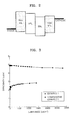
- FIG. 2 is an energy band diagram schematically illustrating differences of highest occupied molecular orbital (HOMO) and lowest unoccupied molecular orbital (LUMO) levels of layers of the organic light emitting device of FIG. 1A , including an anode, a first hole injection layer as described herein, a hole transport layer, an emission layer, a first electron transport layer as described herein, and a cathode.
- HOMO highest occupied molecular orbital
- LUMO lowest unoccupied molecular orbital
- Example 1 Manufacture of organic light emitting device
- a Corning 15 ⁇ /cm 2 (1200 ⁇ ) ITO glass substrate was cut to a size of 50 mm x 50 mm x 0.7 mm and was ultrasonically washed with isopropyl alcohol and pure water for 5 minutes, respectively.
- the ITO glass substrate was irradiated with ultraviolet rays for 30 minutes and washed with ozone.
- NPB and MoOX were co-deposited on the substrate to form a first hole injection layer with a thickness of 100 ⁇ .
- TCTA was coated on the first hole injection layer to form a second hole injection layer.
- NPB was vacuum deposited on the second hole injection layer to form a hole transport layer having a thickness of 60 nm.
- 100 parts by weight of Alq 3 as a host and 5 parts by weight of coumarin 6 as a dopant were vacuum deposited on the hole transport layer to form an emissive layer.
- ETL electron transport layer
- Al was vacuum deposited on the ETL to form a cathode having a thickness of 3000 ⁇ . Thus, the manufacture of an organic light emitting device was completed.
- An organic light emitting device was manufactured in the same manner as in Example 1, except that 50 parts by weight of lithium quinolate and 50 parts by weight of BeBq 2 were vacuum co-deposited to form the electron transport layer.
- a Corning 15 ⁇ /cm 2 (1200 ⁇ ) ITO glass substrate was cut to a size of 50 mm x 50 mm x 0.7 mm and was ultrasonically washed with isopropyl alcohol and pure water for 5 minutes, respectively.
- the ITO glass substrate was irradiated with ultraviolet rays for 30 minutes and washed with ozone.
- a hole injection layer formed of CuPc was formed on the substrate to a thickness of 5 nm.
- NPB was vacuum deposited on the hole injection layer to form a hole transport layer having a thickness of 60 nm.
- 100 parts by weight of Alq 3 as a host and 5 parts by weight of coumarin 6 as a dopant were vacuum deposited on the hole transport layer to form an emissive layer.
- ETL1 first electron transport layer
- Al was vacuum deposited on the ETL1 to form a cathode having a thickness of 3000 ⁇ , that is, an Al electrode. Thus, the manufacture of an organic light emitting device was completed.
- An organic light emitting device was manufactured in the same manner as in Example 1, except that 50 parts by weight of cesium fluoride and 50 parts by weight of BeBq 2 were vacuum co-deposited to form the ETL1.
- An organic light emitting device was manufactured in the same manner as in Example 1, except that a first compound was used in the formation of the electron transport layer.
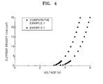
- FIGS. 3 and 4 show that Power efficiency (cd/A) according to luminance (cd/m 2 ) and current density (mA/cm 2 ) according to voltage (V) of the organic light emitting devices manufactured in Example 1 and Comparative Example 1 were measured. The results are shown in the graphs of FIGS. 3 and 4 .
- FIG. 3 shows that the organic light emitting device of Example 1 had a greater efficiency compared to the organic light emitting device Comparative Example 1.
- FIG. 4 shows that the organic light emitting device required less voltage to reach a given current density compared to the organic light emitting device of Comparative Example 1.
- Organic light emitting devices according to the present invention have excellent electrical properties, and use a hole injecting material that is suitable for use in fluorescent and phosphorescent devices with any kind of colors, such as red, green, blue, white, or the like.
- organic light emitting devices according to the present invention use an electron transporting material that provides an improved electron injection ability such that a separate electron injection layer is not necessary. Therefore, compared with the case where a conventional electron transporting material is used, organic light emitting devices according to the present invention using the electron transporting material described herein have improved current and power efficiencies, and have improved driving voltage and lifetime by adjusting the balance of charges injected into the emissive layer.
- organic light emitting devices Due to such configuration of organic light emitting devices according to the present invention, charge injection barriers can be reduced, resulting in reduction in power consumption, and the current efficiency can be maximized by adjusting a charge mobility of the hole injecting and electron transporting materials described herein. In addition, the organic light emitting devices can have higher luminance and longer lifetime.
Landscapes
- Physics & Mathematics (AREA)
- Optics & Photonics (AREA)
- Chemical & Material Sciences (AREA)
- Engineering & Computer Science (AREA)
- Materials Engineering (AREA)
- Organic Chemistry (AREA)
- Electroluminescent Light Sources (AREA)
Abstract
Description
- The present invention relates to an organic light emitting device, and more particularly, to an organic light emitting device with improved driving voltage, light emitting efficiency, lifetime, and the like by using a novel hole injecting material and a novel electron transporting material. In addition, the present invention contributes to development of a high image quality organic light emitting device, and provides an organic light emitting device with reduced power consumption and improved lifetime.
- Organic light emitting devices are devices in which, when a current is supplied to an organic layer interposed between two electrodes, electrons and holes combine in the organic layer to emit light. Such organic light emitting devices can be formed as light-weight and thin information display devices having a high image quality, quick response time, and wide viewing angles. These features have led to rapid development of organic light emitting display device technology. Currently, organic light emitting devices are widely used in mobile phones and other information display devices.
- Due to such rapid development of organic light emitting devices, competition with other information display devices such as TFT-LCDs is inevitable in terms of academic and industrial technology. In addition, conventional organic light emitting devices are limited in terms of the amount of efficiency and lifetime improvements and power consumption reduction that is possible. The need to improve efficiency and reduce power consumption is an important factor interfering with quantitative and qualitative growth of organic light emitting devices, and it is desirable that this issue be resolved.
- The present invention provides an organic light emitting device having reduced power consumption, improved driving voltage, light emitting efficiency and lifetime by introducing a novel hole injecting material and a novel electron transporting material.
- According to a first aspect of the present invention, there is provided an organic light emitting device comprising: a first electrode; a second electrode; an emissive layer disposed between the first electrode and the second electrode; a first hole injection layer disposed between the first electrode and the emissive layer; and a first electron transport layer disposed between the emissive layer and the second electrode, wherein the first hole injection layer comprises a hole injecting material and a first compound comprising an element selected from the group consisting of Mo, Li, Na, K, Rb, Cs, Be, Mg, Ca, Sr, Ba, ytterbium and B and an element selected from the group consisting of O, F, S, Cl, Se, Br, and I, and the first electron transport layer comprises an electron transporting material and a second compound, which is represented by
Formula 1 below:
<Formula 1> XaYb
wherein: - X is an alkali metal, an alkaline earth metal, or a transition metal,
- Y is a group 7 element, or a C1- C20 organic group,
- a is a number in the range of 1 to 3, and
- b is a number in the range of 1 to 3.
- According to an embodiment of the present invention, the organic light emitting device further comprises a second hole injection layer in addition to the first hole injection layer.
- According to an embodiment of the present invention, the organic light emitting device further comprises a second electron transport layer in addition to the first electron transport layer.
- The above and other features of the invention are set out in the appended claims.
- Additional embodiments and/or advantages of the invention will be set forth in part in the description which follows and, in part, will be obvious from the description, or may be learned by practice of the invention.
- These and/or other embodiments and advantages of the invention will become apparent and more readily appreciated from the following description of the embodiments, taken in conjunction with the accompanying drawings of which:
-
FIGS. 1A through 1F are schematic cross-sectional views illustrating structures of organic light emitting devices according to embodiments of the present invention; -
FIG. 2 is an energy band diagram schematically illustrating differences in HOMO and LUMO levels of layers of the organic light emitting device ofFIG. 1A ; -
FIG. 3 is a graph showing efficiency properties of an organic light emitting device according to Example 1 and Comparative Example 1; and -
FIG. 4 is a graph showing current density with respect to voltage of an organic light emitting device according to Example 1 and a Comparative Example 1. - Reference will now be made in detail to preferred embodiments of the present invention, examples of which are illustrated in the accompanying drawings, wherein like reference numerals refer to the like elements throughout. The embodiments are described below in order to explain the present invention by referring to the figures.
- To realize an organic light emitting device with high efficiency performance, the charge balance in an emissive layer is very important. Accordingly, the first aspect of the present invention provides a first hole injection layer including a hole injecting material and a first compound comprising an element selected from the group consisting of Mo, Li, Na, K, Rb, Cs, Be, Mg, Ca, Sr, Ba, B, and ytterbium and an element selected from the group consisting of O, F, S, Cl, Se, Br, and I. In addition, the first aspect of the present invention provides a first electron transport layer including a second compound, which is a metal-containing compound represented by Formula 1 below, and an electron transporting material.
<Formula 1 > XaYb
wherein: - X is an alkali metal, an alkaline earth metal, or a transition metal,
- Y is a group 7 element, or a C1- C20 organic group,
- a is a number in the range of 1 to 3, and
- b is a number in the range of 1 to 3.
- As non-limiting examples, the first compound may be a molybdenum oxide, a magnesium fluoride, a cesium fluoride, a boron oxide, a lithium oxide, an ytterbium oxide, or the like. The first compound may be prepared using various methods that are known to one of ordinary skill in the art.
- The hole injecting material can be any known organic hole injecting material such as, for example, copper phthalocyanine, 1 ,3,5-tricarbazolylbenzene, 4,4'-biscarbazolylbiphenyl, polyvinylcarbazole, m-biscarbazolylphenyl, 4,4'-biscarbazolyl-2,2'-dimethylbiphenyl, 4,4',4"-tri(N-carbazolyl)triphenylamine (TCTA), 4,4',4"-tris(3-methylphenylamino)triphenylamine (m-MTDATA), 1,3,5-tri(2-carbazolylphenyl)benzene, 1,3,5-tris(2-carbazolyl-5-methoxyphenyl)benzene, bis(4-carbazolylphenyl)silane, N,N'-bis(3-methylphenyl)-N,N'-diphenyl-[1,1-biphenyl]-4,4'-diamine (TPD), N,N'-di(naphthalene-1-yl)-N,N'-diphenyl benzidine (α-NPD), N,N'-diphenyl-N,N'-bis(1-naphthyl)-(1,1'-biphenyl)-4,4'-diamine (NPB), poly(9,9-dioctylfluorene-co-N-(4-butylphenyl)diphenylamine) (TFB), poly(9,9-dioctylfluorene-co-bis-N,N-phenyl-1,4-phenylenediamine (PFB), or the like.
- As a non-limiting example, the mixing ratio of the first compound to the hole injecting material may be in the range of 1:1 to 3:1. Although other embodiments of the invention have mixing ratios falling outside this range, it will often be preferred. When the mixing ratio of the first compound to the hole injecting material is less than 1:1, that is, when the amount of the first compound is relatively lower and the amount of the hole injecting material is relatively higher, the injection voltage may be increased. On the other hand, when the mixing ratio of the first compound to the hole transporting material is greater than 3:1, that is, when the amount of the first compound is relatively much higher and the amount of the hole injecting material is relatively lower, the hole injection layer may have insulating properties.
- Conventionally, organic-based materials have been used by themselves for reducing the hole injection barrier. However, when these materials are used, an energy gap may still exist between electrodes and the organic-based material. When the first compound according to the present invention is used on an interface of an electrode, the metallic properties of an element selected from the group consisting of Mo, Li, Na, K, Rb, Cs, Be, Mg, Ca, Sr, Ba, and B can be utilized such that the contact resistance at the electrode interface is decreased, and thus, interface properties of electrodes using a semiconducting compound, ohmic contact, can be obtained.
- An organic light emitting device having such structures described above, according to the present invention, can reduce the hole injection barrier, and also can reduce the contact resistance at the interface of the electrode, and thus, when the organic light emitting device operates, the organic light emitting device can have a longer lifetime.
- An organic light emitting device according to an embodiment of the present invention further includes a second hole injection layer.
- The second hole injection layer may be formed of a conventional organic hole injecting material without including the first compound. For example, the second hole injection layer may comprise at least one hole injecting material selected from the group consisting of copper phthalocyanine, 1,3,5-tricarbazolylbenzene, 4,4'-biscarbazolylbiphenyl, polyvinylcarbazole, m-biscarbazolylphenyl, 4,4'-biscarbazolyl-2,2'-dimethylbiphenyl, 4,4',4"-tri(N-carbazolyl)triphenylamine (TCTA), 4,4',4"-tris(3-methylphenylamino)triphenylamine (m-MTDATA),1,3,5-tri(2-carbazolylphenyl)benzene, 1,3,5-tris(2-carbazolyl-5-methoxyphenyl)benzene, bis(4-carbazolylphenyl)silane, N,N'-bis(3-methylphenyl)-N,N'-diphenyl-[1,1-biphenyl]-4,4'diamine (TPD), N,N'-di(naphthalene-1-yl)-N,N'-diphenyl benzidine (α-NPD), N,N'-diphenyl-N,N'-bis(1-naphthyl)-(1,1'-biphenyl)-4,4'-diamine (NPB), poly(9,9-dioctylfluorene-co-N-(4-butylphenyl)diphenylamine) (TFB), poly(9,9-dioctylfluorene-co-bis-N,N-phenyl-1,4-phenylenediamine (PFB), and the like.
- As described above, when the organic light emitting device of the present invention includes a hole injection layer having a two-layered structure, that is, a first hole injection layer and a second hole injection layer, the effects described above are even more pronounced. When the organic light emitting device includes the second hole injection layer, barriers when holes are transferred to a hole transport layer from the first hole injection layer can be reduced.
- The thickness ratio of the first hole injection layer to the second hole injection layer may be in the range of 1:99 to 1:9. Although other embodiments of the invention have mixing ratios falling outside this range, it will often be preferred. When the thickness ratio of the first hole injection layer to the second hole injection layer is less than 1:99, that is, when the thickness of the first hole injection layer is much thinner with respect to the second hole injection layer, the effect of a reduction in hole injection barrier may be reduced. On the other hand, when the thickness ratio of the first hole injection layer to the second hole injection layer is greater than 1:9, that is, when the thickness of the first hole injection layer is not much thinner with respect to the second hole injection layer, hole transporting ability to an electric field may be reduced.
- The organic light emitting device according to the aspect described above further includes a first electron transport layer that comprises an electron transporting material and a second compound, which is a metal-containing compound represented by
Formula 1, above. InFormula 1, as a non-limiting example, X may be Li, Cs, Na, Ba, or Mg, and Y may be fluoride, quinolate, acetoacetate, chloride, or bromide. When the electron transport layer comprises a halide element, the properties of electron injection from an electrode vary depending on the strength of electronegativity of the halide. Specifically, the second compound may be a metal halide containing a halogen atom, such as lithium fluoride, a metal complex material such as lithium quinolate, lithium acetoacetate, and the like, or mixtures thereof. As specific non-limiting examples, the compound may comprise at least one selected from the group consisting of lithium quinolate, sodium quinolate, lithium acetoacetate, magnesium acetoacetate, lithium fluoride, cesium fluoride, sodium fluoride, and lithium oxide. The first electron transporting material may comprise an electron transporting material having an electron mobility of 10-8 cm2/V•s or more in an electric field of 800 to 1000 V/cm. As non-limiting examples, the first electron transporting material of the first electron transport layer may be Alq3, Bebq2, Znq, or the like - As a non-limiting example, the amount of the second compound, (the metal-containing compound of Formula 1) may be in the range of 30 to 50 parts by weight based on 100 parts by weight of the electron transporting material.
- In the organic light emitting device according to the present invention, an electron injection layer may be omitted without lowering the ability of electron injection in OLEDs.
- In addition, the organic light emitting device may further include a second electron transport layer in addition to the first electron transport layer described above. The second electron transport layer comprises a second electron transporting material, which may be the same as or different from the first electron transporting material. In more detail, the organic light emitting device according to the present invention may include a first electron transport layer comprising the second compound (the metal-containing compound of Formula 1) and a first electron transporting material, and a second electron transport layer comprising a second electron transporting material and not containing the second compound. The second electron transporting material may be the same as the first electron transporting material in terms of electron injection barriers and electron mobility. In particular, the second electron transporting material may have an electron mobility of 10-8 cm2/V•s or more in an electric field of 800 to 1000 V/cm, or more specifically, 10-4 to 10-8 cm2/V•s, in an electric field of 800 to 1000 V/cm, and may be Alq3, Bebq2, Znq, or the like.
- When the organic light emitting device includes the two-layered electron transport layer as described above, a much more systematic electron injection is possible compared with the case where an organic light emitting device includes a single-layered electron transport layer. Thus, power consumption may be significantly reduced due to voltage reduction.
- A separate electron injection layer may be omitted from the organic light emitting device described herein.
- The organic light emitting device according to the present invention may have a variety of structures.
FIGS. 1A through 1F are schematic cross-sectional views illustrating structures of organic light emitting devices according to embodiments of the present invention. - The organic light emitting device may have a structure of an anode, a hole injection layer (HIL), a hole transport layer (HTL), an emissive layer (EML), an electron transport layer (ETL), an electron injection layer (EIL), and a cathode. As specific, non-limiting examples, the organic light emitting device may have one of the following structures:
- first electrode/first hole injection layer/emissive layer/first electron transport layer/second electrode (
FIG. 1A ); - first electrode/first hole injection layer/hole transport layer/emissive layer/first electron transport layer/ electron injection layer/second electrode (
FIG. 1 B) ; - first electrode/first hole injection layer/hole transport layer/emissive layer/hole blocking layer/first electron transport layer/electron injection layer/second electrode (
FIG. 1 C) ; - first electrode/first hole injection layer/second hole injection layer/hole transport layer/emissive layer/first electron transport layer/second electrode (
FIG. 1 D) ; - first electrode/first hole injection layer/hole transport layer/emissive layer/second electron transport layer/first electron transport layer/second electrode (
FIG. 1 E) ; and - first electrode/first hole injection layer/second hole injection layer/hole transport layer/emissive layer/second electron transport layer/first electron transport layer/second electrode (
FIG. 1F ). - The organic light emitting device may further include additional layers, such as one-layered or two-layered intermediate layers, if desired, and may have other structures or layers in addition to the layers shown in
FIGS. 1A - 1F . - Hereinafter, a method of manufacturing an organic light emitting device according to an embodiment of the present invention will be described.
- First, a material for a first electrode material is coated onto a substrate to form a first electrode (typically, an anode). Herein, the substrate may comprise a substrate material typically used in conventional organic light emitting devices. For example, the substrate may be a glass substrate or a plastic substrate having good transparency, surface smoothness, manageability and waterproofness. The material for the anode can be a transparent and highly conductive material, such as ITO, IZO, SnO2, ZnO, or the like.
- Next, a hole injection layer (HIL) is formed on the first electrode using various methods such as vacuum deposition, spin coating, casting, Langmuir Blodgett (LB) deposition, or the like.
- When the HIL is formed by vacuum deposition, vacuum deposition conditions may vary according to the compound used to form the HIL, and the desired structure and thermal properties of the HIL to be formed. In general, however, the vacuum deposition may be performed at a deposition temperature of 50-500°C, a pressure of 10-8 -10-3 torr, and a deposition speed of 0.01-100 Å/sec. The thickness of the HIL may be in the range of 10Å to 5µm.
- Next, a hole transport layer (HTL) is formed on the HIL using a hole transporting material. The HTL may be formed by vacuum deposition, spin coating, casting, LB deposition, or the like; for example, the HTL may be formed on the HIL by vacuum deposition such that a uniform film may be easily formed and so that pin holes are not easily formed. When the HTL is formed by vacuum deposition, the deposition conditions may vary according to the compound used to form the HTL. In general, however, the deposition conditions may be similar to those used for the formation of the HIL.
- The hole transporting material is not particularly limited, and may be N,N'-bis(3-methylphenyl)-N,N'-diphenyl-[1,1-biphenyl]-4,4'-diamine (TPD), N,N'-di(naphthalene-1-yl)-N,N'-diphenyl benzidine (α-NPD), or the like.
- Next, an emissive layer (EML) is formed on the HTL. The EML can be formed by vacuum deposition, spin coating, casting, LB deposition, or the like.
- The material for forming the EML is not particularly limited. As non-limiting examples, the material for forming the EML may be a blue emitting material such as oxadiazole dimer dyes (such as Bis-DAPOXP), spiro compounds (such as Spiro-DPVBi, Spiro-6P), triarylamine compounds, bis(styryl)amine compounds (such as DPVBi, DSA), 4,4'-bis(9-ethyl-3-carbazovinylene)-1,1'-biphenyl (BCzVBi), perylene, 2,5,8,11-tetra-tert-butylperylene (TPBe), 9H-carbazole-3,3'-(1,4-phenylene-di-2,1-ethene-diyl)bis[9-ethyl-(9C)] (BCzVB), 4,4-bis[4-(di-p-tolylamino)styryl]biphenyl (DPAVBi), 4-(di-p-tolylamino)-4'-[(di-p-tolylamino)styryl]stylbene (DPAVB), 4,4'-bis[4-(diphenylamino)styryl]biphenyl (BDAVBi), bis(3,5-difluoro-2-(2-pyridyl)phenyl-(2-carboxypyridyl)iridium III (FlrPic), or the like; a green emitting material such as 3-(2-benzothiazolyl)-7-(diethylamino)coumarin (Coumarin 6), 2,3,6,7-tetrahydro-1,1,7,7, tetramethyl-1H,5H,11H-10-(2-benzothiazolyl)quinolizino-[9,9a,1gh]coumarin (C545T), N,N'-dimethyl-quinacridone (DMQA), tris(2-phenylpyridine)iridium (III) (Ir(ppy)3), or the like; or a red emitting material such as tetraphenylnaphthacene (Rubrene), tris(1-phenylisoquinoline)iridium (III) (Ir(piq)3), bis(2-benzo[b]thiophene-2-yl-pyridine) (acetylacetonate)iridium (III) (Ir(btp)2(acac)), tris(dibenzoylmethane)phenanthroline europium (III) (Eu(dbm)3(phen)), tris[4,4'-di-tert-butyl-(2,2')-bipyridine]ruthenium (III) complex (Ru(dtb-bpy)3*2(PF6)), DCM1, DCM2, Eu (thenoyltrifluoroacetone)3 (Eu(TTA)3), butyl-6-(1,1,7,7-tetramethyljulolidyl-9-enyl)-4H-pyran (DCJTB), or the like. In addition, the material for forming the EML may include as a polymer emitting material an aromatic compound comprising nitrogen and polymers such as phenylenes, phenylene vinylenes, thiophenes, fluorenes, spiro-fluorenes, or the like; however, the present invention is not limited thereto.
- The thickness of the EML may be in the range of 10 to 500 nm, or more specifically, in the range of 50 to 120 nm. In particular, as a specific, non-limiting example, the thickness of the EML when formed of a blue emitting material may be 70 nm. When the thickness of the EML is less than 10 nm, the leakage current can increase so that the efficiency of the organic light emitting device decreases. On the other hand, when the thickness of the EML is greater than 500 nm, the driving voltage can increase.
- If desired, the EML can be prepared by adding an emissive dopant to a host for the EML. As non-limiting examples, the fluorescent host material may be tris(8-hydroxy-quinolinato)aluminum (Alq3), 9,10-di(naphth-2-yl)anthracene (AND), 3-Tert-butyl-9,10-di(naphth-2-yl)anthracene (TBADN), 4,4'-bis(2,2-diphenyl-ethene-1-yl)-4,4'-biphenyl (DPVBi), 4,4'-bis(2,2-diphenyl-ethene-1-yl)-4,4'-dimethylphenyl (p-DMDPVBi), Tert(9,9-diarylfluorene)s (TDAF), 2-(9,9'-spirobifluorene-2-yl)-9,9'-spirobifluorene (BSDF), 2,7-bis(9,9'-spirobifluorene-2-yl)-9,9'-spirobifluorene (TSDF), bis(9,9-diarylfluorene)s (BDAF), 4,4'-bis(2,2-diphenyl-ethene-1-yl)-4,4'-di-(tert-butyl)phenyl (p-TDPVBi), or the like. As non-limiting examples, the phosphorescence host material may be 1,3-bis(carbazol-9-yl)benzene (mCP), 1,3,5-tris(carbazol-9-yl)benzene (tCP), 4,4',4"-tris(carbazol-9-yl)triphenylamine (TcTa), 4,4'-bis(carbazol-9-yl)biphenyl (CBP), 4,4'-Bis(9-carbazolyl)-2,2'-dimethyl-biphenyl (CBDP), 4,4'-bis(carbazol-9-yl)-9,9-dimethyl-fluorene (DMFL-CBP), 4,4'-bis(carbazol-9-yl)-9,9-bis(9-phenyl-9H-carbazol)fluorene (FL-4CBP), 4,4'-bis(carbazol-9-yl)-9,9-di-tolyl-fluorene (DPFL-CBP), 9,9-bis(9-phenyl-9H-carbazol)fluorene (FL-2CBP), or the like.
- As specific, non-limiting examples, the dopant may be 4,4'-bis[4-(di-p-tolylamino)styryl]biphenyl (DPAVBi), and the fluorescence host may be 9,10-di(naphth-2-yl)anthracene (ADN) or 3-tert-butyl-9,10-di(naphth-2-yl)anthracene (TBADN).


- The amount of the dopant varies according to the particular material that forms the EML. In general, however, the amount of the dopant may be in the range of 3-80 parts by weight based on 100 parts by weight of the material that forms the EML (total weight of host and dopant). If the amount of the dopant is outside this range, light emitting properties of the organic light emitting device may be degraded.
- Next, an electron transport layer (ETL) is formed on the EML using an electron transporting material and the second compound (that is, the metal-containing compound of Formula 1). The ETL may be formed by vacuum deposition. The electron transporting material may be an electron transporting material having an electron mobility of 10-8 cm2/V•s or more, preferably in the range of 10-3 to 10-8 cm2/V•s, in an electric field of 800 to 1000 V/cm. If the electron mobility of the electron transport layer is less than 10-8 cm2/V•s, electron injection to the EML may be excessive, resulting in poor charge balance.
- As non-limiting examples, the electron transporting material may be bis(10-hydroxybenzo[h]quinolinato)beryllium (Bebq2) represented by
Formula 2 below, Alq3, Znq2, or the like.
- In addition, an electron injection layer may be omitted from the organic light emitting device according to the present invention and the organic light emitting device may still exhibit an excellent electron injection ability. However, when an electron injection layer (EIL) that facilitates electron injection from a cathode is formed on the ETL, the electron injection ability is significantly improved.
- As non-limiting examples, the material for forming the EIL may be LiF, NaCl, CsF, Li2O, BaO, or the like. The deposition conditions of the ETL and the EIL may vary according to the compounds used to form the ETL and the EIL. In general, however, the deposition conditions are similar to those used for the formation of the HIL.
- Finally, a cathode, a second electrode, is formed on the EIL using a metal material. The cathode may be formed by vacuum deposition, sputtering, or the like. Herein, the metal material is selected to have a low work function and may be a metal, an alloy, an electrically conductive compound, or a mixture thereof. As particular non-limiting examples, the metal used to form the cathode may be Li, Mg, Al, Al-Li, Ca, Mg-In, Mg-Ag, or the like, and the cathode may be formed of a transparent material such as ITO, or IZO in order to manufacture a top emission organic light emitting device.
- A method of manufacturing an organic light emitting device according to another embodiment of the present invention will now be described. The method of manufacturing an organic light emitting device according to this embodiment is similar to that of the previous embodiment except that a second electron transport layer is formed on the EML by vacuum depositing a second electron transporting material and a first electron transport layer is formed on the second electron transport layer by vacuum depositing a first electron transporting material and second compound (the metal-containing compound of Formula 1).
-
FIG. 2 is an energy band diagram schematically illustrating differences of highest occupied molecular orbital (HOMO) and lowest unoccupied molecular orbital (LUMO) levels of layers of the organic light emitting device ofFIG. 1A , including an anode, a first hole injection layer as described herein, a hole transport layer, an emission layer, a first electron transport layer as described herein, and a cathode. - Hereinafter, aspects of the present invention will be described in greater detail with reference to the following examples. The following examples are for illustrative purposes only and are not intended to limit the scope of the invention.
- As an anode, a
Corning 15 Ω/cm2 (1200 Å) ITO glass substrate was cut to a size of 50 mm x 50 mm x 0.7 mm and was ultrasonically washed with isopropyl alcohol and pure water for 5 minutes, respectively. The ITO glass substrate was irradiated with ultraviolet rays for 30 minutes and washed with ozone. - Then, NPB and MoOX were co-deposited on the substrate to form a first hole injection layer with a thickness of 100Å. Subsequently, TCTA was coated on the first hole injection layer to form a second hole injection layer.
- NPB was vacuum deposited on the second hole injection layer to form a hole transport layer having a thickness of 60 nm. After the formation of the hole transport layer, 100 parts by weight of Alq3 as a host and 5 parts by weight of
coumarin 6 as a dopant were vacuum deposited on the hole transport layer to form an emissive layer. - Then, 30 parts by weight of LiF and 70 parts by weight of BeBq2 were vacuum co-deposited on the emissive layer to form an electron transport layer (ETL) having a thickness of 35 nm.
- Al was vacuum deposited on the ETL to form a cathode having a thickness of 3000Å. Thus, the manufacture of an organic light emitting device was completed.
- An organic light emitting device was manufactured in the same manner as in Example 1, except that 50 parts by weight of lithium quinolate and 50 parts by weight of BeBq2 were vacuum co-deposited to form the electron transport layer.
- As an anode, a
Corning 15 Ω/cm2 (1200 Å) ITO glass substrate was cut to a size of 50 mm x 50 mm x 0.7 mm and was ultrasonically washed with isopropyl alcohol and pure water for 5 minutes, respectively. The ITO glass substrate was irradiated with ultraviolet rays for 30 minutes and washed with ozone. - A hole injection layer formed of CuPc was formed on the substrate to a thickness of 5 nm.
- NPB was vacuum deposited on the hole injection layer to form a hole transport layer having a thickness of 60 nm. After the formation of the hole transport layer, 100 parts by weight of Alq3 as a host and 5 parts by weight of
coumarin 6 as a dopant were vacuum deposited on the hole transport layer to form an emissive layer. - Then, BeBq2 was vacuum deposited on the emissive layer to form a second electron transport layer (ETL2) having a thickness of 10 nm.
- 50 parts by weight of LiF and 50 parts by weight of BeBq2 were vacuum co-deposited on the ETL2 to form a first electron transport layer (ETL1) having a thickness of 20 nm.
- Al was vacuum deposited on the ETL1 to form a cathode having a thickness of 3000Å, that is, an Al electrode. Thus, the manufacture of an organic light emitting device was completed.
- An organic light emitting device was manufactured in the same manner as in Example 1, except that 50 parts by weight of cesium fluoride and 50 parts by weight of BeBq2 were vacuum co-deposited to form the ETL1.
- An organic light emitting device was manufactured in the same manner as in Example 1, except that a first compound was used in the formation of the electron transport layer.
- Power efficiency (cd/A) according to luminance (cd/m2) and current density (mA/cm2) according to voltage (V) of the organic light emitting devices manufactured in Example 1 and Comparative Example 1 were measured. The results are shown in the graphs of
FIGS. 3 and4 .FIG. 3 shows that the organic light emitting device of Example 1 had a greater efficiency compared to the organic light emitting device Comparative Example 1.FIG. 4 shows that the organic light emitting device required less voltage to reach a given current density compared to the organic light emitting device of Comparative Example 1. - Organic light emitting devices according to the present invention have excellent electrical properties, and use a hole injecting material that is suitable for use in fluorescent and phosphorescent devices with any kind of colors, such as red, green, blue, white, or the like. In addition, organic light emitting devices according to the present invention use an electron transporting material that provides an improved electron injection ability such that a separate electron injection layer is not necessary. Therefore, compared with the case where a conventional electron transporting material is used, organic light emitting devices according to the present invention using the electron transporting material described herein have improved current and power efficiencies, and have improved driving voltage and lifetime by adjusting the balance of charges injected into the emissive layer. Due to such configuration of organic light emitting devices according to the present invention, charge injection barriers can be reduced, resulting in reduction in power consumption, and the current efficiency can be maximized by adjusting a charge mobility of the hole injecting and electron transporting materials described herein. In addition, the organic light emitting devices can have higher luminance and longer lifetime.
Claims (19)
- An organic light emitting device comprising:a first electrode;a second electrode;an emissive layer disposed between the first electrode and the second electrode;a first hole injection layer disposed between the first electrode and the emissive layer; anda first electron transport layer disposed between the emissive layer and the second electrode,wherein the first hole injection layer comprises a hole injecting material and a first compound comprising an element selected from the group consisting of Mo, Li, Na, K, Rb, Cs, Be, Mg, Ca, Sr, Ba, ytterbium and B and an element selected from the group consisting of O, F, S, Cl, Se, Br, and I, and
the first electron transport layer comprises a first electron transporting material and a second compound, wherein the second compound is represented by Formula 1 below:
<Formula 1> XaYb
wherein:X is an alkali metal, an alkaline earth metal, or a transition metal,Y is a group 7 element, or a C1- C20 organic group,a is a number in the range of from 1 to 3, andb is a number in the range of from 1 to 3. - An organic light emitting device according to claim 1, wherein the hole injecting material is at least one selected from the group consisting of copper phthalocyanine, 1,3,5-tricarbazolylbenzene, 4,4'- biscarbazolylbiphenyl, polyvinylcarbazole, m-biscarbazolylphenyl, 4,4'-biscarbazolyl-2,2'-dimethylbiphenyl, 4,4',4"-tri(N-carbazolyl)triphenylamine (TCTA), 4,4',4"-tris(3-methylphenylamino)triphenylamine (m-MTDATA), 1,3,5-tri(2-carbazolylphenyl)benzene, 1 ,3,5-tris(2-carbazolyl-5-methoxyphenyl)benzene, bis(4-carbazolylphenyl)silane, N,N'-bis(3-methylphenyl)-N,N'-diphenyl-[1,1-biphenyl]-4,4'-diamine (TPD), N,N'-di(naphthalene-1-yl)-N,N'-diphenyl benzidine (α -NPD), N,N'-diphenyl-N,N'-bis(1-naphthyl)-(1,1'-biphenyl)-4,4'-diamine (NPB), poly(9,9-dioctylfluorene-co-N-(4-butylphenyl)diphenylamine) (TFB), and poly(9,9-dioctylfluorene-co-bis-N,N-phenyl-1,4-phenylenediamine (PFB).
- An organic light emitting device according to claim 1 or 2, wherein the mixing ratio of the first compound to the hole injecting material is in the range of from 1:1 to 3:1.
- An organic light emitting device according to any of claims 1-3, wherein the first compound is selected from the group consisting of a molybdenum oxide, a magnesium fluoride, a cesium fluoride, a boron oxide, a lithium oxide, and an ytterbium oxide.
- An organic light emitting device according to any of claims 1-4, further comprising a second hole injection layer disposed between the first hole injection layer and the emissive layer and comprising a second hole injecting material.
- An organic light emitting device according to claim 5, wherein the second hole injecting material is at least one selected from the group consisting of copper phthalocyanine, 1,3,5-tricarbazolylbenzene, 4,4'- biscarbazolylbiphenyl, polyvinylcarbazole, m-biscarbazolylphenyl, 4,4'-biscarbazolyl-2,2'-dimethylbiphenyl, 4,4',4"-tri(N-carbazolyl)triphenylamine (TCTA), 4,4',4"-tris(3-methylphenylamino)triphenylamine (m-MTDATA), 1,3,5-tri(2-carbazolylphenyl)benzene, 1,3,5-tris(2-carbazolyl-5-methoxyphenyl)benzene, bis(4-carbazolylphenyl)silane, N,N'-bis(3-methylphenyl)-N,N'-diphenyl-[1,1-biphenyl]-4,4'-diamine (TPD), N,N'-di(naphthalene-1-yl)-N,N'-diphenyl benzidine (α -NPD), N,N'-diphenyl-N,N'-bis(1-naphthyl)-(1,1'-biphenyl)-4,4'-diamine (NPB), poly(9,9-dioctylfluorene-co-N-(4-butylphenyl)diphenylamine) (TFB), and poly(9,9-dioctylfluorene-co-bis-N,N-phenyl-1,4-phenylenediamine (PFB).
- An organic light emitting device according to claim 5 or 6, wherein the thickness ratio of the first hole injection layer to the second hole injection layer is in the range of from 1:99 to 1:9.
- An organic light emitting device according to any preceding claim, wherein, in Formula 1, X is Li, Cs, Na, Ba, or Mg.
- An organic light emitting device according to any preceding claim 1, wherein, in Formula 1, Y is quinolate, acetoacetate, fluoride, chloride, or bromide.
- An organic light emitting device according to any of claims 1-7, wherein the second compound comprises at least one selected from the group consisting of lithium quinolate, sodium quinolate, lithium acetoacetate, magnesium acetoacetate, lithium fluoride, cesium fluoride, and sodium fluoride.
- An organic light emitting device according to any preceding claim, wherein the amount of the second compound is in the range of from 30 to 50 parts by weight based on 100 parts by weight of the first electron transporting material.
- An organic light emitting device according to any preceding claim, wherein the first electron transporting material has an electron mobility of 10-8 cm2/V•S or more in an electric field of from 800 to 1000 V/cm.
- An organic light emitting device according to any preceding claim, wherein the first electron transporting material comprises at least one selected from the group consisting of bis(10-hydroxybenzo[h]quinolinato)beryllium (Bebq2) represented by Formula 2 below, Alq3, and Znq2.

- An organic light emitting device according to any preceding claim, further comprising a second electron transport layer comprising a second electron transporting material.
- An organic light emitting device according to claim 14, wherein the second electron transporting material has an electron mobility of 10-8 cm2/V•s or more in an electric field of from 800 to 1000 V/cm.
- An organic light emitting device according to claim 14 or 15, wherein the second electron transporting material has an electron mobility of from 10-4 to 10-8 cm2/V•s or more in an electric field of 800 to 1000 V/cm.
- An organic light emitting device according to any of claims 14-16, wherein the thickness ratio of the first electron transport layer to the second electron transport layer is in the range of from 1:1 to 2:1.
- An organic light emitting device according to claim 1, further comprising at least one layer selected from the group consisting of a second hole injection layer, a hole transport layer, an electron blocking layer, a hole blocking layer, a second electron transport layer, and an electron injection layer.
- An organic light emitting device according to claim 1, having one of the following structures:first electrode/first hole injection layer/emissive layer/first electron transport layer/second electrode;first electrode/first hole injection layer/hole transport layer/emissive layer/first electron transport layer/electron injection layer/second electrode;first electrode/first hole injection layer/hole transport layer/emissive layer/hole blocking layer/first electron transport layer/electron injection layer/second electrode;first electrode/first hole injection layer/second hole injection layer/hole transport layer/emissive layer/first electron transport layer/second electrode;first electrode/first hole injection layer/hole transport layer/emissive layer/second electron transport layer/first electron transport layer/second electrode; andfirst electrode/first hole injection layer/second hole injection layer/hole transport layer/emissive layer/second electron transport layer/first electron transport layer/second electrode.
Applications Claiming Priority (1)
| Application Number | Priority Date | Filing Date | Title |
|---|---|---|---|
| KR1020070136406A KR100918401B1 (en) | 2007-12-24 | 2007-12-24 | Organic light emitting device |
Publications (2)
| Publication Number | Publication Date |
|---|---|
| EP2075858A1 true EP2075858A1 (en) | 2009-07-01 |
| EP2075858B1 EP2075858B1 (en) | 2013-04-17 |
Family
ID=40474709
Family Applications (1)
| Application Number | Title | Priority Date | Filing Date |
|---|---|---|---|
| EP20080254128 Active EP2075858B1 (en) | 2007-12-24 | 2008-12-23 | Organic light emitting device |
Country Status (5)
| Country | Link |
|---|---|
| US (1) | US8557398B2 (en) |
| EP (1) | EP2075858B1 (en) |
| JP (1) | JP4903190B2 (en) |
| KR (1) | KR100918401B1 (en) |
| CN (1) | CN101488561B (en) |
Cited By (2)
| Publication number | Priority date | Publication date | Assignee | Title |
|---|---|---|---|---|
| EP2999019A1 (en) * | 2014-09-19 | 2016-03-23 | Novaled GmbH | Organic light-emitting diode including an electron transport layer stack comprising different lithium compounds and elemental metal |
| EP3024045A1 (en) * | 2014-11-18 | 2016-05-25 | EverDisplay Optronics (Shanghai) Limited | Blue light organic light-emitting diode and display including same |
Families Citing this family (27)
| Publication number | Priority date | Publication date | Assignee | Title |
|---|---|---|---|---|
| JP5560996B2 (en) * | 2009-07-31 | 2014-07-30 | 大日本印刷株式会社 | Device material for hole injection transport layer, ink for forming hole injection transport layer, device having hole injection transport layer, and method for producing the same |
| EP2367215A1 (en) * | 2010-03-15 | 2011-09-21 | Novaled AG | An organic photoactive device |
| KR101708421B1 (en) * | 2010-08-23 | 2017-02-21 | 삼성디스플레이 주식회사 | Organic light emitting diode display |
| JP5447356B2 (en) | 2010-12-09 | 2014-03-19 | セイコーエプソン株式会社 | Display device and electronic device |
| KR101730554B1 (en) | 2010-12-30 | 2017-04-26 | 엘지디스플레이 주식회사 | Organic electroluminescent device |
| JP2012182443A (en) * | 2011-02-11 | 2012-09-20 | Semiconductor Energy Lab Co Ltd | Light-emitting element and light-emitting device |
| CN102738400B (en) * | 2011-03-31 | 2015-11-25 | 海洋王照明科技股份有限公司 | A kind of white-light electroluminescence device |
| KR101933952B1 (en) * | 2011-07-01 | 2018-12-31 | 가부시키가이샤 한도오따이 에네루기 켄큐쇼 | Light-emitting device, electronic device, and lighting device |
| WO2013078595A1 (en) * | 2011-11-28 | 2013-06-06 | 海洋王照明科技股份有限公司 | Organic electroluminescent device having ternary doped hole transportation layer and preparation method therefor |
| KR101671343B1 (en) * | 2012-05-22 | 2016-11-02 | 삼성디스플레이 주식회사 | Organic light emitting device and method for pruducing the same |
| US10374187B2 (en) * | 2012-05-22 | 2019-08-06 | Samsung Display Co., Ltd. | Organic light-emitting device and method of producing the same |
| KR20140008126A (en) * | 2012-07-10 | 2014-01-21 | 삼성디스플레이 주식회사 | Organic light emitting device |
| CN104051635A (en) * | 2013-03-11 | 2014-09-17 | 海洋王照明科技股份有限公司 | Organic light-emitting device and preparation method thereof |
| CN104078575A (en) * | 2013-03-29 | 2014-10-01 | 海洋王照明科技股份有限公司 | Organic light-emitting diode and preparation method thereof |
| CN103367653B (en) * | 2013-07-10 | 2016-02-03 | 上海和辉光电有限公司 | Inversion type organic light emitting diodde desplay device and preparation method thereof |
| KR102084170B1 (en) * | 2013-07-25 | 2020-03-04 | 삼성디스플레이 주식회사 | An organic light emitting device, an organic light emitting display appratus having the organic light emitting device and a method of manufacturing the same |
| US9935271B2 (en) * | 2014-01-15 | 2018-04-03 | Jilin Universtiy | Organic electroluminescent device based on neutral free-radical electroluminescent material |
| JP6728603B2 (en) * | 2015-09-08 | 2020-07-22 | コニカミノルタ株式会社 | Organic electroluminescence element and vehicle lamp |
| JP6664514B2 (en) * | 2016-05-10 | 2020-03-13 | エルジー・ケム・リミテッド | Organic electroluminescent device and method of manufacturing the same |
| KR102078435B1 (en) * | 2016-07-14 | 2020-02-17 | 주식회사 엘지화학 | Organic light emitting diode and manufacturing method of the same |
| JP6686787B2 (en) * | 2016-08-12 | 2020-04-22 | 株式会社デンソー | Organic EL display device and manufacturing method thereof |
| CN106784346B (en) * | 2016-12-08 | 2019-05-07 | Tcl集团股份有限公司 | Metal oxide modified QLED device and preparation method thereof |
| CN106601924A (en) * | 2016-12-21 | 2017-04-26 | 浙江大学 | Quantum dot light emitting diode and preparation method thereof |
| US12342673B2 (en) * | 2019-10-29 | 2025-06-24 | Sharp Kabushiki Kaisha | Light emitting element, light emitting device, and display device |
| KR102820733B1 (en) * | 2020-08-21 | 2025-06-16 | 삼성디스플레이 주식회사 | Organic light-emitting diode and manufacturing the same |
| WO2022061939A1 (en) * | 2020-09-28 | 2022-03-31 | 京东方科技集团股份有限公司 | Organic electroluminescent device and display device |
| KR20220102708A (en) * | 2021-01-13 | 2022-07-21 | 삼성디스플레이 주식회사 | Light-emitting device and electronic apparatus including the same |
Citations (4)
| Publication number | Priority date | Publication date | Assignee | Title |
|---|---|---|---|---|
| EP1603174A2 (en) * | 2004-06-03 | 2005-12-07 | Lg Electronics Inc. | Organic electroluminescent device |
| EP1631125A1 (en) * | 2003-05-20 | 2006-03-01 | Idemitsu Kosan Co., Ltd. | Organic electroluminescent device and display |
| WO2006109878A1 (en) * | 2005-04-11 | 2006-10-19 | Semiconductor Energy Laboratory Co., Ltd. | Light-emitting element, light-emitting device, and vapor deposition apparatus |
| US20060292394A1 (en) * | 2005-06-22 | 2006-12-28 | Semiconductor Energy Laboratory Co., Ltd. | Light emitting device and electronic appliance using the same |
Family Cites Families (51)
| Publication number | Priority date | Publication date | Assignee | Title |
|---|---|---|---|---|
| JP4486713B2 (en) | 1997-01-27 | 2010-06-23 | 淳二 城戸 | Organic electroluminescent device |
| JPH10270171A (en) * | 1997-01-27 | 1998-10-09 | Junji Kido | Organic electroluminescent device |
| KR100263754B1 (en) | 1997-10-10 | 2000-08-16 | 김덕중 | Process and equipment for the preparation of organic light emitting device having improved ohmic contact |
| JP4505067B2 (en) | 1998-12-16 | 2010-07-14 | 淳二 城戸 | Organic electroluminescent device |
| JP2000215984A (en) | 1999-01-26 | 2000-08-04 | Matsushita Electric Works Ltd | Organic electroluminescent element |
| US7306856B2 (en) * | 2000-07-17 | 2007-12-11 | Fujifilm Corporation | Light-emitting element and iridium complex |
| JP2003264083A (en) | 2002-03-08 | 2003-09-19 | Sharp Corp | Organic LED element and manufacturing method thereof |
| JPWO2004028217A1 (en) | 2002-09-20 | 2006-01-19 | 出光興産株式会社 | Organic electroluminescence device |
| TWI265750B (en) * | 2003-02-27 | 2006-11-01 | Toyota Jidoshokki Kk | Organic electro-luminescence devices |
| CN1781340A (en) | 2003-02-27 | 2006-05-31 | 株式会社丰田自动织机 | organic electroluminescent element |
| KR100501702B1 (en) * | 2003-03-13 | 2005-07-18 | 삼성에스디아이 주식회사 | Organic electroluminescent display device |
| JP3877692B2 (en) * | 2003-03-28 | 2007-02-07 | 三洋電機株式会社 | Organic electroluminescence device and method for manufacturing the same |
| KR100560778B1 (en) * | 2003-04-17 | 2006-03-13 | 삼성에스디아이 주식회사 | Organic electroluminescent display device |
| JP2004355975A (en) | 2003-05-29 | 2004-12-16 | Sony Corp | Display device manufacturing method |
| KR20050015902A (en) | 2003-08-14 | 2005-02-21 | 엘지전자 주식회사 | Organic electroluminescence device and fabrication method of the same |
| JP4718768B2 (en) * | 2003-09-19 | 2011-07-06 | 株式会社半導体エネルギー研究所 | Light emitting device |
| JP3748110B1 (en) | 2003-09-26 | 2006-02-22 | 株式会社半導体エネルギー研究所 | LIGHT EMITTING DEVICE AND ELECTRONIC DEVICE USING THE SAME |
| JP4276109B2 (en) | 2004-03-01 | 2009-06-10 | ローム株式会社 | Organic electroluminescent device |
| KR20060135801A (en) | 2004-03-05 | 2006-12-29 | 이데미쓰 고산 가부시키가이샤 | Organic electroluminescent element and organic electroluminescent display |
| JP3813616B2 (en) | 2004-03-22 | 2006-08-23 | 三洋電機株式会社 | Organic electroluminescence device |
| US7195829B2 (en) * | 2004-03-30 | 2007-03-27 | Eastman Kodak Company | Organic element for electroluminescent devices |
| US20060008670A1 (en) * | 2004-07-06 | 2006-01-12 | Chun Lin | Organic light emitting materials and devices |
| JP4925569B2 (en) | 2004-07-08 | 2012-04-25 | ローム株式会社 | Organic electroluminescent device |
| KR100721554B1 (en) | 2004-07-22 | 2007-05-23 | 삼성에스디아이 주식회사 | Organic electroluminescent device and manufacturing method thereof |
| JP4823629B2 (en) | 2004-09-24 | 2011-11-24 | 株式会社半導体エネルギー研究所 | Light emitting device |
| KR101205192B1 (en) * | 2004-10-01 | 2012-11-27 | 가부시키가이샤 한도오따이 에네루기 켄큐쇼 | Light emitting element and light emitting device |
| JP4999308B2 (en) | 2004-10-01 | 2012-08-15 | 株式会社半導体エネルギー研究所 | Light emitting element and light emitting device |
| JP5878272B2 (en) * | 2005-03-23 | 2016-03-08 | 株式会社半導体エネルギー研究所 | COMPOSITE MATERIAL, LIGHT EMITTING ELEMENT, LIGHT EMITTING DEVICE AND ELECTRIC DEVICE |
| JP3903187B2 (en) | 2005-03-24 | 2007-04-11 | 国立大学法人信州大学 | Organic electroluminescence device |
| WO2006115232A1 (en) | 2005-04-21 | 2006-11-02 | Semiconductor Energy Laboratory Co., Ltd. | Light emitting element, light emitting device, and electronic device |
| JP5116992B2 (en) | 2005-05-27 | 2013-01-09 | 富士フイルム株式会社 | Organic EL device |
| US7687986B2 (en) * | 2005-05-27 | 2010-03-30 | Fujifilm Corporation | Organic EL device having hole-injection layer doped with metallic oxide |
| US20060286405A1 (en) * | 2005-06-17 | 2006-12-21 | Eastman Kodak Company | Organic element for low voltage electroluminescent devices |
| KR100672535B1 (en) | 2005-07-25 | 2007-01-24 | 엘지전자 주식회사 | Organic electroluminescence device and method for fabricating the same |
| KR100806812B1 (en) | 2005-07-25 | 2008-02-25 | 엘지.필립스 엘시디 주식회사 | Organic EL element and its manufacturing method |
| KR20070036835A (en) * | 2005-09-30 | 2007-04-04 | 삼성전자주식회사 | Method for manufacturing an organic light emitting device comprising an inorganic buffer layer |
| JP2007134677A (en) | 2005-10-11 | 2007-05-31 | Fujifilm Corp | Organic electroluminescence device |
| US20070090756A1 (en) * | 2005-10-11 | 2007-04-26 | Fujifilm Corporation | Organic electroluminescent element |
| JP2007109868A (en) * | 2005-10-13 | 2007-04-26 | Sanyo Electric Co Ltd | Thin film transistor and organic electroluminescence display device |
| TWI299636B (en) * | 2005-12-01 | 2008-08-01 | Au Optronics Corp | Organic light emitting diode |
| US8454748B2 (en) * | 2005-12-27 | 2013-06-04 | Semiconductor Energy Laboratory Co., Ltd. | Method of calculating carrier mobility |
| KR100698300B1 (en) | 2005-12-29 | 2007-03-22 | 엘지전자 주식회사 | Organic EL element and its manufacturing method |
| KR100741104B1 (en) | 2005-12-30 | 2007-07-20 | 삼성에스디아이 주식회사 | Organic light emitting device |
| KR101313094B1 (en) * | 2006-01-24 | 2013-12-31 | 삼성디스플레이 주식회사 | Polymer with 1,8-naphthalimide unit and Organic Electroluminescence Device containing the same |
| JP5063007B2 (en) | 2006-02-06 | 2012-10-31 | 富士フイルム株式会社 | Organic electroluminescence device |
| US7968904B2 (en) * | 2006-02-06 | 2011-06-28 | Fujifilm Corporation | Organic electroluminescence device |
| US9112170B2 (en) * | 2006-03-21 | 2015-08-18 | Semiconductor Energy Laboratory Co., Ltd. | Light-emitting element, light-emitting device, and electronic device |
| JP4943199B2 (en) | 2006-03-21 | 2012-05-30 | 株式会社半導体エネルギー研究所 | Oxadiazole derivatives |
| WO2007123061A1 (en) | 2006-04-20 | 2007-11-01 | Idemitsu Kosan Co., Ltd. | Organic light-emitting device |
| KR101386216B1 (en) * | 2006-06-07 | 2014-04-18 | 삼성디스플레이 주식회사 | Organic light emitting device |
| KR100922760B1 (en) * | 2008-03-03 | 2009-10-21 | 삼성모바일디스플레이주식회사 | Organic light emitting device |
-
2007
- 2007-12-24 KR KR1020070136406A patent/KR100918401B1/en active Active
-
2008
- 2008-06-05 US US12/133,843 patent/US8557398B2/en not_active Expired - Fee Related
- 2008-10-20 JP JP2008270210A patent/JP4903190B2/en not_active Expired - Fee Related
- 2008-12-23 EP EP20080254128 patent/EP2075858B1/en active Active
- 2008-12-24 CN CN200810184444XA patent/CN101488561B/en active Active
Patent Citations (4)
| Publication number | Priority date | Publication date | Assignee | Title |
|---|---|---|---|---|
| EP1631125A1 (en) * | 2003-05-20 | 2006-03-01 | Idemitsu Kosan Co., Ltd. | Organic electroluminescent device and display |
| EP1603174A2 (en) * | 2004-06-03 | 2005-12-07 | Lg Electronics Inc. | Organic electroluminescent device |
| WO2006109878A1 (en) * | 2005-04-11 | 2006-10-19 | Semiconductor Energy Laboratory Co., Ltd. | Light-emitting element, light-emitting device, and vapor deposition apparatus |
| US20060292394A1 (en) * | 2005-06-22 | 2006-12-28 | Semiconductor Energy Laboratory Co., Ltd. | Light emitting device and electronic appliance using the same |
Non-Patent Citations (1)
| Title |
|---|
| WALZER K ET AL: "Highly Efficient Organic Devices Based on Electrically Doped Transport Layers", CHEMICAL REVIEWS, AMERICAN CHEMICAL SOCIETY, WASHINGTON, DC, US, vol. 107, 1 January 2007 (2007-01-01), pages 1233 - 1271, XP007908268 * |
Cited By (3)
| Publication number | Priority date | Publication date | Assignee | Title |
|---|---|---|---|---|
| EP2999019A1 (en) * | 2014-09-19 | 2016-03-23 | Novaled GmbH | Organic light-emitting diode including an electron transport layer stack comprising different lithium compounds and elemental metal |
| EP3024045A1 (en) * | 2014-11-18 | 2016-05-25 | EverDisplay Optronics (Shanghai) Limited | Blue light organic light-emitting diode and display including same |
| US9673415B2 (en) | 2014-11-18 | 2017-06-06 | Everdisplay Optronics (Shanghai) Limited | Blue light organic light-emitting diode and display including same |
Also Published As
| Publication number | Publication date |
|---|---|
| KR20090068693A (en) | 2009-06-29 |
| JP4903190B2 (en) | 2012-03-28 |
| CN101488561B (en) | 2013-06-19 |
| CN101488561A (en) | 2009-07-22 |
| US20090160319A1 (en) | 2009-06-25 |
| JP2009152178A (en) | 2009-07-09 |
| US8557398B2 (en) | 2013-10-15 |
| EP2075858B1 (en) | 2013-04-17 |
| KR100918401B1 (en) | 2009-09-24 |
Similar Documents
| Publication | Publication Date | Title |
|---|---|---|
| EP2075858B1 (en) | Organic light emitting device | |
| JP4903234B2 (en) | Organic light emitting device | |
| KR100922760B1 (en) | Organic light emitting device | |
| KR100922755B1 (en) | Organic light emitting device | |
| EP2610937B1 (en) | Organic light emitting device with enhanced lifespan | |
| KR100922757B1 (en) | Organic light emitting device with improved lifespan | |
| US7973467B2 (en) | Organic light emitting device | |
| KR20120010438A (en) | Organic light emitting device | |
| KR100879476B1 (en) | Organic light emitting device | |
| EP2355625A2 (en) | Low voltage-driven organic electroluminescence device, and manufacturing method thereof | |
| KR100894066B1 (en) | Organic light emitting device | |
| US20090315024A1 (en) | Organic luminescence device | |
| EP1603174B1 (en) | Organic electroluminescent device | |
| KR100898075B1 (en) | Organic light emitting device |
Legal Events
| Date | Code | Title | Description |
|---|---|---|---|
| PUAI | Public reference made under article 153(3) epc to a published international application that has entered the european phase |
Free format text: ORIGINAL CODE: 0009012 |
|
| 17P | Request for examination filed |
Effective date: 20090105 |
|
| AK | Designated contracting states |
Kind code of ref document: A1 Designated state(s): AT BE BG CH CY CZ DE DK EE ES FI FR GB GR HR HU IE IS IT LI LT LU LV MC MT NL NO PL PT RO SE SI SK TR |
|
| AX | Request for extension of the european patent |
Extension state: AL BA MK RS |
|
| RAP1 | Party data changed (applicant data changed or rights of an application transferred) |
Owner name: SAMSUNG SDI CO., LTD. |
|
| AKX | Designation fees paid |
Designated state(s): DE FR GB HU |
|
| RAP1 | Party data changed (applicant data changed or rights of an application transferred) |
Owner name: SAMSUNG MOBILE DISPLAY CO., LTD. |
|
| 17Q | First examination report despatched |
Effective date: 20110527 |
|
| GRAP | Despatch of communication of intention to grant a patent |
Free format text: ORIGINAL CODE: EPIDOSNIGR1 |
|
| RAP1 | Party data changed (applicant data changed or rights of an application transferred) |
Owner name: SAMSUNG DISPLAY CO., LTD. |
|
| GRAS | Grant fee paid |
Free format text: ORIGINAL CODE: EPIDOSNIGR3 |
|
| GRAP | Despatch of communication of intention to grant a patent |
Free format text: ORIGINAL CODE: EPIDOSNIGR1 |
|
| GRAA | (expected) grant |
Free format text: ORIGINAL CODE: 0009210 |
|
| AK | Designated contracting states |
Kind code of ref document: B1 Designated state(s): DE FR GB HU |
|
| REG | Reference to a national code |
Ref country code: GB Ref legal event code: FG4D |
|
| REG | Reference to a national code |
Ref country code: DE Ref legal event code: R096 Ref document number: 602008023862 Country of ref document: DE Effective date: 20130613 |
|
| PLBE | No opposition filed within time limit |
Free format text: ORIGINAL CODE: 0009261 |
|
| STAA | Information on the status of an ep patent application or granted ep patent |
Free format text: STATUS: NO OPPOSITION FILED WITHIN TIME LIMIT |
|
| 26N | No opposition filed |
Effective date: 20140120 |
|
| REG | Reference to a national code |
Ref country code: DE Ref legal event code: R097 Ref document number: 602008023862 Country of ref document: DE Effective date: 20140120 |
|
| PG25 | Lapsed in a contracting state [announced via postgrant information from national office to epo] |
Ref country code: HU Free format text: LAPSE BECAUSE OF FAILURE TO SUBMIT A TRANSLATION OF THE DESCRIPTION OR TO PAY THE FEE WITHIN THE PRESCRIBED TIME-LIMIT; INVALID AB INITIO Effective date: 20081223 |
|
| REG | Reference to a national code |
Ref country code: FR Ref legal event code: PLFP Year of fee payment: 8 |
|
| REG | Reference to a national code |
Ref country code: FR Ref legal event code: PLFP Year of fee payment: 9 |
|
| REG | Reference to a national code |
Ref country code: FR Ref legal event code: PLFP Year of fee payment: 10 |
|
| REG | Reference to a national code |
Ref country code: DE Ref legal event code: R079 Ref document number: 602008023862 Country of ref document: DE Free format text: PREVIOUS MAIN CLASS: H01L0051500000 Ipc: H10K0050000000 |
|
| P01 | Opt-out of the competence of the unified patent court (upc) registered |
Effective date: 20230515 |
|
| PGFP | Annual fee paid to national office [announced via postgrant information from national office to epo] |
Ref country code: DE Payment date: 20241121 Year of fee payment: 17 |
|
| PGFP | Annual fee paid to national office [announced via postgrant information from national office to epo] |
Ref country code: GB Payment date: 20241121 Year of fee payment: 17 |
|
| PGFP | Annual fee paid to national office [announced via postgrant information from national office to epo] |
Ref country code: FR Payment date: 20241121 Year of fee payment: 17 |