EP2070168B1 - Überspannungsableiter mit einem gehäuse und mit mindestens einem ableitelement - Google Patents
Überspannungsableiter mit einem gehäuse und mit mindestens einem ableitelement Download PDFInfo
- Publication number
- EP2070168B1 EP2070168B1 EP08831283A EP08831283A EP2070168B1 EP 2070168 B1 EP2070168 B1 EP 2070168B1 EP 08831283 A EP08831283 A EP 08831283A EP 08831283 A EP08831283 A EP 08831283A EP 2070168 B1 EP2070168 B1 EP 2070168B1
- Authority
- EP
- European Patent Office
- Prior art keywords
- bridge
- conductive element
- short
- surge arrester
- conductor section
- Prior art date
- Legal status (The legal status is an assumption and is not a legal conclusion. Google has not performed a legal analysis and makes no representation as to the accuracy of the status listed.)
- Active
Links
Images


Classifications
-
- H—ELECTRICITY
- H01—ELECTRIC ELEMENTS
- H01T—SPARK GAPS; OVERVOLTAGE ARRESTERS USING SPARK GAPS; SPARKING PLUGS; CORONA DEVICES; GENERATING IONS TO BE INTRODUCED INTO NON-ENCLOSED GASES
- H01T1/00—Details of spark gaps
- H01T1/14—Means structurally associated with spark gap for protecting it against overload or for disconnecting it in case of failure
Definitions
- the invention relates to a surge arrester having a housing and at least one diverting element, for example a varistor, as well as a separating device for disconnecting the diverter element (s) from the mains, the divider device comprising a soldering point which is integrated into the electrical connection path inside the diverter, wherein via the solder joint, a movable conductor section or a movable conductive bridge with the discharge element on the one hand and the conductor section or the bridge on the other hand connected to a first electrical external terminal of the arrester, and comprising a biasing force generating means, such as spring, wherein the relevant force vector directly or indirectly over a movable separating block acts on the conductor section or the bridge in the separating direction, according to the preamble of patent claim 1 as an addition to German patent application no. 10 2006 052 955.3 ,
- the low-resistance short circuit path thus connected may be e.g. be used to actuate an upstream switching element, which is set to the short-circuit current of the relevant network, or to produce a defined continuous short circuit, which is defined in certain applications as a so-called fail-safe state.
- the switching element is a changeover contact.
- the changeover contact closes the varistor circuit in a known manner via a soldering point. If the switching element is triggered, another contact is closed, which can be connected either as an internal or external defect indicator or just via a corresponding external connection as a short circuit.
- the prior art includes the arrangement for dissipating overvoltages, wherein a plurality of overvoltage limiting elements, such as varistors or diodes, and eg by overheating or detection of the leakage current triggering switching means are provided according to DE 41 24 321 C2 ,
- a plurality of overvoltage limiting elements such as varistors or diodes, and eg by overheating or detection of the leakage current triggering switching means are provided according to DE 41 24 321 C2
- at least two overvoltage limiting elements are arranged, of which each element is sufficiently dimensioned for itself to ensure the overvoltage protection at the relevant site.
- a thermal cut-off in the sense of a thermal fuse monitors the leakage current of the overvoltage limiting elements, so that, for example, a first element can be switched off when overheating and a second element can be switched on.
- a surge protection device which comprises at least one varistor and a shutdown device connected in series with the varistor.
- the cut-off device responds to unacceptable heating of the varistor in such a way that due to the heat load, an existing solder joint is separated.
- the solder connection consists of at least one varistor connection and a prestressed metallic spring and the heat transport to the solder takes place via the connecting wire of the varistor.
- known separation devices for surge arresters are equipped with an additional connection that extends the existing disconnection function by a short-circuit function, which leads to the fault current for a limited time. It is suggested that the additional Connection to design various, so that even when needed, an activation from the outside of the corresponding realized surge arrester is possible.
- the separating device comprises a solder joint with a solder which melts at the corresponding response temperature.
- the separating device can also be realized by other melting materials, which themselves have no conductive properties, namely, when the electrical connection to the connection path is made via a bridge part whose mechanical position is secured by means of the melting material.
- At least one conductive element is arranged in the movement path of the spring-biased conductor or the spring-biased bridge, the first end of which comes into contact with the conductor section or the bridge when the disconnecting device is triggered.
- the second end of the conductive element is in communication with a second external electrical connection.
- means are provided for protecting the contact point between the conductor section or bridge and the conductive element before wegspratzenden Lotresten or solder material or the aforementioned melting materials.
- the conductive element is designed as a bridge-like bracket whose second end is connectable to the external electrical connection when tightening a clamp provided for this purpose. In this way, the assembly is simplified because the bridge-like bracket does not need to be contacted separately.
- the first end of the conductive element has a quasi-flat or slightly curved plate shape, wherein the plate has a substantially parallel orientation to the conductor portion or to the bridge, with respect to the separation case.
- the plate may have on its underside directed to the second end of a recess or a recess for receiving wegspratzendem solder or melting material. In this way, it is effectively prevented that solder deposits on the plate and forms raised areas there, with the consequence of an undesirable contact resistance.
- the recess is also able to absorb any eroded material of the conductor section or the bridge.
- the conductive element can be subsequently inserted into the arrester in order to realize not only a disconnect but also a short-circuit fail-safe function.
- the preferably provided bridge-like bracket as a conductive element has means for attachment to or in the arrester housing.
- the conductive element is dimensioned or designed so that after a predetermined time, the short-circuit function is canceled.
- the means for fastening may e.g. a groove or a recess in the bracket and a complementary thereto nose or a counter-groove in the housing for producing a positive connection include. Special modifications of such a fastener are of course the possible alternatives.
- a Isolierplättchen between the conductive element and the conductor portion or the bridge can be arranged.
- the conductive element can be provided at least on its first end with a detachable insulating coating, for example in the form of an insulating tube.
- a detachable insulating coating for example in the form of an insulating tube.
- the insulating plate and the insulating coating can be removed via a suitable opening in the housing to release the additional function "short circuit".
- the relative distance between the conductive member and the conductor portion or the bridge can be adjusted. It is important to accomplish in a first position that the conductor section or bridge in the separation case comes into sufficient contact with the conductive element. On the other hand, it can be prevented by a Wegbegrenzung with respect to the conductor portion or the bridge, that the conductive element is touched. It is conceivable in this embodiment, the arrangement of a travel or stroke limiting, adjustable eccentric.
- short circuiter may be in a complementary embodiment in the path of movement of the conductor portion or the bridge, a limiting element, e.g. be used in the form of a pin, bolt or similar stop.
- the insulating plate or the pin or bolt accessible from outside through the housing, in particular in order to be able to subsequently remove these means.
- the respectively activated short-circuit function can be signaled via a display. It can also be provided to seal the access to remove the insulating plate, the pin or the bolt. An example thinkable plug-like seal takes with the removal of the insulating plate or the pin or the bolt. Such a seal-free surge arrester indicates the intended additional short-circuit function.
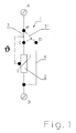
- FIG. 1 A varistor 2 is connected between the external terminals A and B.
- This varistor 2 can be cut off via a separating device (switching tongue) 3, which is thermally triggered. Between the points a and c there is usually an electrical connection via a conductor section or a bridge, in the non-triggered state.
- the separating device 1 In state 3 ', the separating device 1 is triggered and it was a compound on the way a to b using a shorting bar 4 made, which bridges the varistor 2.
- the actuated or triggered short-circuit state is shown by dashed lines between the points a and b according to figure. Recalling the Fig. 2 to 5 the switching movement after the soldering of a solder under the influence of a compression spring 6 (reference numeral 11 in FIG Fig. 6 and 6 b ).
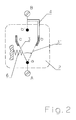
- the Fig. 2 schematically shows the execution of a switching device 1 with disconnection and short-circuit function in the non-actuated or not triggered state.
- the actuated, ie triggered short-circuit state is according to Fig. 2 in the representation between the points a and b shown in dashed lines.
- the switching movement takes place after the Auslötvorgang under the influence of the force of the spring 6.
- the tongue 3, which forms the conductor portion is thus used simultaneously to realize the desired short circuit between the connection points A and B by these in abutment with the conductive Element or the shorting bar 4 passes.
- an insulating plate 7 is arranged so that the switching tongue 3 or 3 'can not get into contact with the shorting bar 4. This means that the movement path of the switching tongue 3, 3 'is limited by the insulating plate 7.
- a pin or a bolt use find or it is possible to cover at least the dashed end of the shorting bar 4 with a removable insulating tube.
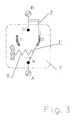
- a movable part 4' of the shorting bar with respect to the rigid bracket part 4" can be changed, so that, as in the Fig. 5b indicated, an InWallet hear with the switching tab 3 can be realized, resulting in the position of the movable part of the shorting bar 4 'after Fig. 5a not possible.
- a stop 9 is provided in this embodiment.
- the eccentric 8 can easily via an opening in the housing shown in dashed lines in its various positions according to the illustrations Fig. 5a and 5b be adjusted, which also becomes clear by the apparent free operating end of the eccentric 8, which respective state (short circuit or not) is present.
- a surge arrester with additional short-circuit function is integrated in a housing 10.
- a pivotally mounted Abtrennbocks 13 and the tension spring 11 acts a bias on the switching tab 3, which is connected by means of a solder 14 with a guided through the housing partition 15 terminal 16 of a (not shown) varistor.
- the conductive member is according to the embodiment according to Fig. 6 designed as a bridge-like bracket 17.
- This bridge-like bracket 17 has a first end in plate form 18.
- a second end of the bridge-like bracket 17 is connected to an external electrical connection when tightening a clamp provided for this purpose 19 in connection.
- the plate-shaped end 18 of the bridge-like bracket 17 has on its underside directed to the second end a recess 20 for receiving in the separation case possibly wegspratzendem solder from the soldering point 14.
- the bridge-like bracket 17 can be fixed via means for fastening 21 on or in the arrester housing 10.
- the distance between the plate-shaped end 18 of the conductive element and the conductor portion or the switching tongue 3 can be adjusted or changed by bending or bending the plate-shaped end 18.
- Decisive is the angular position of the plate-shaped end 18 with respect to the position of the switching tongue 3. In any case, here is to ensure that for the desired safe short circuit, the switching tab 3 over a large area and just with the plate-shaped end 18 comes into contact.
- the advanced surge arrester with short-circuit function can be easily accommodated in a standard housing for DIN rail mounting, wherein the bridge-like bracket 17 is easily accessible after removal of the housing cover, not shown. It can be provided on the mounting side a surge arrester without, but also with short-circuit function with little effort, which can be realized by subsequent insertion of the bridge-like bracket 17 and a later short circuit function.
- FIG. 6b shows a representation of the separation device according to the invention in a realized device in the tripped state (switch position triggered b).
- the recess 20 in the region of the plate-shaped end 18 of the bridge-like bracket 17 is such that the soldering point 14 of the tongue 3 does not come into contact with the bridge-like bracket 17. Possibly adhering or splashing solder may pass through the clearance provided by the recess 20 and does not result in a possibly excessive contact resistance.
- solder paste solder point 14 and 14 ' (see FIG. 6a ) not involved in the actual large-scale contact. Only the part b of the switching tongue 3 'abuts on the surface of the plate-shaped end 18 of the bridge-like bracket 17.
- FIG. 7 shows a schematic diagram with a conductive element, which is designed as a switching device SE.
- the bypass formed by the switching device in the event of a short circuit is not designed here for continuous current carrying capacity. After the fault current has flowed over a certain time, the bypass is switched off. Due to the desired undersizing, the conductive element can have smaller cross sections of the electrically conductive parts and can therefore be manufactured more cost-effectively.
- the conductive element may be formed as a fuse or else have a power semiconductor or form a circuit with a power semiconductor, wherein the power semiconductor is transferred after passing a short-circuit current by means of an initial pulse in the open state.
- the functions assigned to the conductive element are the symbolic representations of a semiconductor switch or a fuse in the FIG. 7 , right side shown.
- the connection of the thermal separator moves to position 2, ie to the connection point for the short-circuit element in the bypass.
- the short-circuit element SE is closed.
- the resulting during the opening of the thermal separation device arc is guided by the contact elements and extinguished independently when reaching the short-circuit contact.
- the switching device SE Immediately after reaching of the short-circuit contact of the arc and the current flows through the bypass, ie via the switching device SE.
- the switching device SE After a predetermined time, the switching device SE opens and it is interrupted, the fault current.
- the switching device according to the invention can be integrated in the surge arrester, but also the combination with an external switching device is possible. After the shutdown process, the defective overvoltage protection device is disconnected from the circuit, but the power supply is maintained. To initiate the opening operation of the switching device SE after a defined time, the switching device z. B. are formed by a cross-section reduction quasi as a fuse.
Landscapes
- Emergency Protection Circuit Devices (AREA)
- Fuses (AREA)
- Thermistors And Varistors (AREA)
Priority Applications (1)
| Application Number | Priority Date | Filing Date | Title |
|---|---|---|---|
| PL08831283T PL2070168T3 (pl) | 2007-10-30 | 2008-10-29 | Ochronnik przepięciowy z obudową i co najmniej jednym elementem ochronnym |
Applications Claiming Priority (2)
| Application Number | Priority Date | Filing Date | Title |
|---|---|---|---|
| DE102007051854.6A DE102007051854B4 (de) | 2006-11-09 | 2007-10-30 | Überspannungsableiter mit einem Gehäuse und mit mindestens einem Ableitelement |
| PCT/EP2008/064672 WO2009056565A1 (de) | 2007-10-30 | 2008-10-29 | Überspannungsableiter mit einem gehäuse und mit mindestens einem ableitelement |
Publications (2)
| Publication Number | Publication Date |
|---|---|
| EP2070168A1 EP2070168A1 (de) | 2009-06-17 |
| EP2070168B1 true EP2070168B1 (de) | 2010-07-28 |
Family
ID=40342142
Family Applications (1)
| Application Number | Title | Priority Date | Filing Date |
|---|---|---|---|
| EP08831283A Active EP2070168B1 (de) | 2007-10-30 | 2008-10-29 | Überspannungsableiter mit einem gehäuse und mit mindestens einem ableitelement |
Country Status (7)
| Country | Link |
|---|---|
| EP (1) | EP2070168B1 (pl) |
| CN (1) | CN101842947B (pl) |
| AT (1) | ATE476004T1 (pl) |
| DE (2) | DE102007051854B4 (pl) |
| PL (1) | PL2070168T3 (pl) |
| RU (1) | RU2474937C2 (pl) |
| WO (1) | WO2009056565A1 (pl) |
Families Citing this family (10)
| Publication number | Priority date | Publication date | Assignee | Title |
|---|---|---|---|---|
| DE102008016589A1 (de) * | 2008-03-31 | 2009-10-01 | Weidmüller Interface GmbH & Co. KG | Schutzvorrichtung |
| SI23303A (sl) | 2010-02-19 | 2011-08-31 | ISKRA ZAŠČITE d.o.o. | Prenapetostni odklopnik z rotacijskim diskom in elektronskim sklopom za izboljšanje zanesljivosti delovanja |
| DE102010047244A1 (de) | 2010-10-04 | 2012-04-05 | Phoenix Contact Gmbh & Co. Kg | Überspannungsschutzvorrichtung |
| DE102011011254A1 (de) | 2010-12-08 | 2012-06-14 | Dehn + Söhne Gmbh + Co. Kg | Überspannungsableiteranordnung mit mindestens einem Varistorableitelement |
| SI23749A (sl) | 2011-05-11 | 2012-11-30 | ISKRA@ZAŠČITE@d@o@o | Redudančni prenapetostni odklopnik z rotacijskimdiskom in z dodanim elektronskim sklopom za zagotavljanje podaljšanja življenjske dobe prenapetostnega gradnika |
| DE102013003584B3 (de) * | 2013-03-01 | 2014-04-03 | Dehn + Söhne Gmbh + Co. Kg | Abtrenn- und Umschaltvorrichtung für den Überspannungsschutz |
| DE202013002222U1 (de) * | 2013-03-07 | 2013-06-24 | Dehn + Söhne Gmbh + Co. Kg | Überspannungsschutzeinrichtung mit Kurzschlussfunktion zum Anlagen- und Personenschutz |
| DE102016011076A1 (de) * | 2016-04-19 | 2017-10-19 | DEHN + SÖHNE GmbH + Co. KG. | Anordnung zum Überlastschutz von Überspannungsschutzgeräten |
| DE102017107871B3 (de) | 2017-04-11 | 2018-08-09 | Dehn + Söhne Gmbh + Co. Kg | Abtrenn- und Umschaltvorrichtung für den Überspannungsschutz, insbesondere für DC-Systeme |
| KR102438378B1 (ko) * | 2018-06-15 | 2022-08-31 | 지멘스 에너지 글로벌 게엠베하 운트 코. 카게 | 방압 장치를 구비한 서지 피뢰기 |
Family Cites Families (8)
| Publication number | Priority date | Publication date | Assignee | Title |
|---|---|---|---|---|
| DE3734214A1 (de) * | 1987-10-09 | 1989-04-20 | Dehn & Soehne | Anordnung zur abschaltung eines varistors |
| DE3820272C1 (pl) * | 1987-10-20 | 1989-04-06 | Krone Ag, 1000 Berlin, De | |
| DE4026004A1 (de) * | 1990-08-14 | 1992-02-20 | Krone Ag | Schutzschaltung und schutzstecker in telekommunikationsanlagen |
| DE4124321C2 (de) * | 1991-07-23 | 2003-10-09 | Dehn & Soehne | Anordnung zur Ableitung von Überspannungen |
| DE9115238U1 (de) | 1991-12-05 | 1992-02-13 | Siemens AG, 8000 München | Überspannungsschutzgerät |
| AT405350B (de) | 1997-02-12 | 1999-07-26 | Felten & Guilleaume Ag Oester | Schutzschaltungsanordnung für überspannungsableiter |
| DE102006000919A1 (de) * | 2006-01-05 | 2007-07-19 | Dehn + Söhne Gmbh + Co. Kg | Steckbarer Überspannungsableiter mit einem oder mehreren Überspannungsschutzelementen |
| DE102006052955B4 (de) * | 2006-09-07 | 2020-07-02 | Dehn Se + Co Kg | Überspannungsableiter mit einem Gehäuse und mit mindestens einem Ableitelement |
-
2007
- 2007-10-30 DE DE102007051854.6A patent/DE102007051854B4/de not_active Expired - Fee Related
-
2008
- 2008-10-29 EP EP08831283A patent/EP2070168B1/de active Active
- 2008-10-29 WO PCT/EP2008/064672 patent/WO2009056565A1/de not_active Ceased
- 2008-10-29 RU RU2010120019/07A patent/RU2474937C2/ru not_active IP Right Cessation
- 2008-10-29 DE DE502008001020T patent/DE502008001020D1/de active Active
- 2008-10-29 CN CN200880113696.1A patent/CN101842947B/zh active Active
- 2008-10-29 AT AT08831283T patent/ATE476004T1/de active
- 2008-10-29 PL PL08831283T patent/PL2070168T3/pl unknown
Also Published As
| Publication number | Publication date |
|---|---|
| CN101842947B (zh) | 2014-03-26 |
| DE502008001020D1 (de) | 2010-09-09 |
| ATE476004T1 (de) | 2010-08-15 |
| DE102007051854A1 (de) | 2009-05-07 |
| RU2474937C2 (ru) | 2013-02-10 |
| WO2009056565A1 (de) | 2009-05-07 |
| RU2010120019A (ru) | 2011-12-10 |
| DE102007051854B4 (de) | 2017-05-04 |
| EP2070168A1 (de) | 2009-06-17 |
| PL2070168T3 (pl) | 2011-03-31 |
| CN101842947A (zh) | 2010-09-22 |
Similar Documents
| Publication | Publication Date | Title |
|---|---|---|
| EP2059933B1 (de) | Überspannungsableiter mit einem gehäuse und mit mindestens einem ableitelement | |
| EP2070168B1 (de) | Überspannungsableiter mit einem gehäuse und mit mindestens einem ableitelement | |
| EP2826044B1 (de) | Überspannungsschutzgerät | |
| EP3120372B1 (de) | Überspannungsschutzeinrichtung, umfassend mindestens einen überspannungsableiter und eine dem überspannungsableiter parallel geschaltete, thermisch auslösbare, federvorgespannte kurzschlussschalteinrichtung | |
| DE102008013447B4 (de) | Überspannungsableiter mit einem Gehäuse und mindestens einem Ableitelement | |
| EP2208208B1 (de) | Überspannungsableiter mit einem gehäuse und mindestens einem ableitelement, insbesondere einem varistor | |
| EP2553691A1 (de) | Überspannungsschutzeinrichtung, umfassend mindestens einen überspannungsableiter | |
| DE102017107871B3 (de) | Abtrenn- und Umschaltvorrichtung für den Überspannungsschutz, insbesondere für DC-Systeme | |
| EP3552282A1 (de) | Überspannungsschutzanordnung, bestehend aus einer in einem isolierenden gehäuse befindlichen hörnerfunkenstrecke | |
| DE3228471A1 (de) | Ueberspannungsschutzgeraet | |
| EP2697881A1 (de) | Zweistufige abschaltvorrichtung | |
| WO2013072467A9 (de) | Verfahren und schaltungsanordnung zum trennen einer elektrischen verbindung zwischen zwei anschlusspunkten | |
| EP2151026B1 (de) | Kurzschliesseinrichtung für überspannungsableiter | |
| EP0951046A2 (de) | Fehlerstromschutzschalter | |
| LU505555B1 (de) | Trennschalter | |
| EP2962319B1 (de) | Abtrenn- und umschaltvorrichtung für den überspannungsschutz | |
| DE202012000339U1 (de) | Elektrische Abtrennvorrichtung | |
| DE102017221937A1 (de) | Anordnung zur elektrischen Überwachung des Schaltzustandes einer Schmelzsicherung | |
| EP0966087B1 (de) | Überspannungsschutzschaltung | |
| EP3057118B1 (de) | Schaltmechanik, brandschutzschalter und system | |
| DE202009004427U1 (de) | Varistor-Überspannungsableiter | |
| EP2070169A1 (de) | Überspannungsableiter mit mindestens einem ableitelement, insbesondere einem varistor, sowie mit einer abtrennvorrichtung |
Legal Events
| Date | Code | Title | Description |
|---|---|---|---|
| PUAI | Public reference made under article 153(3) epc to a published international application that has entered the european phase |
Free format text: ORIGINAL CODE: 0009012 |
|
| 17P | Request for examination filed |
Effective date: 20090324 |
|
| AK | Designated contracting states |
Kind code of ref document: A1 Designated state(s): AT BE BG CH CY CZ DE DK EE ES FI FR GB GR HR HU IE IS IT LI LT LU LV MC MT NL NO PL PT RO SE SI SK TR |
|
| 17Q | First examination report despatched |
Effective date: 20090811 |
|
| GRAP | Despatch of communication of intention to grant a patent |
Free format text: ORIGINAL CODE: EPIDOSNIGR1 |
|
| GRAS | Grant fee paid |
Free format text: ORIGINAL CODE: EPIDOSNIGR3 |
|
| GRAA | (expected) grant |
Free format text: ORIGINAL CODE: 0009210 |
|
| AK | Designated contracting states |
Kind code of ref document: B1 Designated state(s): AT BE BG CH CY CZ DE DK EE ES FI FR GB GR HR HU IE IS IT LI LT LU LV MC MT NL NO PL PT RO SE SI SK TR |
|
| REG | Reference to a national code |
Ref country code: GB Ref legal event code: FG4D Free format text: NOT ENGLISH |
|
| REG | Reference to a national code |
Ref country code: CH Ref legal event code: EP |
|
| REG | Reference to a national code |
Ref country code: IE Ref legal event code: FG4D Free format text: LANGUAGE OF EP DOCUMENT: GERMAN |
|
| REF | Corresponds to: |
Ref document number: 502008001020 Country of ref document: DE Date of ref document: 20100909 Kind code of ref document: P |
|
| REG | Reference to a national code |
Ref country code: NL Ref legal event code: VDEP Effective date: 20100728 |
|
| LTIE | Lt: invalidation of european patent or patent extension |
Effective date: 20100728 |
|
| PG25 | Lapsed in a contracting state [announced via postgrant information from national office to epo] |
Ref country code: NO Free format text: LAPSE BECAUSE OF FAILURE TO SUBMIT A TRANSLATION OF THE DESCRIPTION OR TO PAY THE FEE WITHIN THE PRESCRIBED TIME-LIMIT Effective date: 20101028 Ref country code: NL Free format text: LAPSE BECAUSE OF FAILURE TO SUBMIT A TRANSLATION OF THE DESCRIPTION OR TO PAY THE FEE WITHIN THE PRESCRIBED TIME-LIMIT Effective date: 20100728 Ref country code: FI Free format text: LAPSE BECAUSE OF FAILURE TO SUBMIT A TRANSLATION OF THE DESCRIPTION OR TO PAY THE FEE WITHIN THE PRESCRIBED TIME-LIMIT Effective date: 20100728 Ref country code: LT Free format text: LAPSE BECAUSE OF FAILURE TO SUBMIT A TRANSLATION OF THE DESCRIPTION OR TO PAY THE FEE WITHIN THE PRESCRIBED TIME-LIMIT Effective date: 20100728 |
|
| PG25 | Lapsed in a contracting state [announced via postgrant information from national office to epo] |
Ref country code: BG Free format text: LAPSE BECAUSE OF FAILURE TO SUBMIT A TRANSLATION OF THE DESCRIPTION OR TO PAY THE FEE WITHIN THE PRESCRIBED TIME-LIMIT Effective date: 20101028 Ref country code: SI Free format text: LAPSE BECAUSE OF FAILURE TO SUBMIT A TRANSLATION OF THE DESCRIPTION OR TO PAY THE FEE WITHIN THE PRESCRIBED TIME-LIMIT Effective date: 20100728 Ref country code: CY Free format text: LAPSE BECAUSE OF FAILURE TO SUBMIT A TRANSLATION OF THE DESCRIPTION OR TO PAY THE FEE WITHIN THE PRESCRIBED TIME-LIMIT Effective date: 20100728 Ref country code: HR Free format text: LAPSE BECAUSE OF FAILURE TO SUBMIT A TRANSLATION OF THE DESCRIPTION OR TO PAY THE FEE WITHIN THE PRESCRIBED TIME-LIMIT Effective date: 20100728 Ref country code: IS Free format text: LAPSE BECAUSE OF FAILURE TO SUBMIT A TRANSLATION OF THE DESCRIPTION OR TO PAY THE FEE WITHIN THE PRESCRIBED TIME-LIMIT Effective date: 20101128 |
|
| REG | Reference to a national code |
Ref country code: IE Ref legal event code: FD4D |
|
| PG25 | Lapsed in a contracting state [announced via postgrant information from national office to epo] |
Ref country code: SE Free format text: LAPSE BECAUSE OF FAILURE TO SUBMIT A TRANSLATION OF THE DESCRIPTION OR TO PAY THE FEE WITHIN THE PRESCRIBED TIME-LIMIT Effective date: 20100728 Ref country code: LV Free format text: LAPSE BECAUSE OF FAILURE TO SUBMIT A TRANSLATION OF THE DESCRIPTION OR TO PAY THE FEE WITHIN THE PRESCRIBED TIME-LIMIT Effective date: 20100728 Ref country code: GR Free format text: LAPSE BECAUSE OF FAILURE TO SUBMIT A TRANSLATION OF THE DESCRIPTION OR TO PAY THE FEE WITHIN THE PRESCRIBED TIME-LIMIT Effective date: 20101029 |
|
| REG | Reference to a national code |
Ref country code: PL Ref legal event code: T3 |
|
| PG25 | Lapsed in a contracting state [announced via postgrant information from national office to epo] |
Ref country code: IE Free format text: LAPSE BECAUSE OF FAILURE TO SUBMIT A TRANSLATION OF THE DESCRIPTION OR TO PAY THE FEE WITHIN THE PRESCRIBED TIME-LIMIT Effective date: 20100728 Ref country code: DK Free format text: LAPSE BECAUSE OF FAILURE TO SUBMIT A TRANSLATION OF THE DESCRIPTION OR TO PAY THE FEE WITHIN THE PRESCRIBED TIME-LIMIT Effective date: 20100728 |
|
| BERE | Be: lapsed |
Owner name: DEHN + SOHNE G.M.B.H. + CO KG Effective date: 20101031 |
|
| PG25 | Lapsed in a contracting state [announced via postgrant information from national office to epo] |
Ref country code: CZ Free format text: LAPSE BECAUSE OF FAILURE TO SUBMIT A TRANSLATION OF THE DESCRIPTION OR TO PAY THE FEE WITHIN THE PRESCRIBED TIME-LIMIT Effective date: 20100728 Ref country code: SK Free format text: LAPSE BECAUSE OF FAILURE TO SUBMIT A TRANSLATION OF THE DESCRIPTION OR TO PAY THE FEE WITHIN THE PRESCRIBED TIME-LIMIT Effective date: 20100728 Ref country code: RO Free format text: LAPSE BECAUSE OF FAILURE TO SUBMIT A TRANSLATION OF THE DESCRIPTION OR TO PAY THE FEE WITHIN THE PRESCRIBED TIME-LIMIT Effective date: 20100728 Ref country code: MC Free format text: LAPSE BECAUSE OF NON-PAYMENT OF DUE FEES Effective date: 20101031 Ref country code: EE Free format text: LAPSE BECAUSE OF FAILURE TO SUBMIT A TRANSLATION OF THE DESCRIPTION OR TO PAY THE FEE WITHIN THE PRESCRIBED TIME-LIMIT Effective date: 20100728 |
|
| PLBE | No opposition filed within time limit |
Free format text: ORIGINAL CODE: 0009261 |
|
| STAA | Information on the status of an ep patent application or granted ep patent |
Free format text: STATUS: NO OPPOSITION FILED WITHIN TIME LIMIT |
|
| PG25 | Lapsed in a contracting state [announced via postgrant information from national office to epo] |
Ref country code: ES Free format text: LAPSE BECAUSE OF FAILURE TO SUBMIT A TRANSLATION OF THE DESCRIPTION OR TO PAY THE FEE WITHIN THE PRESCRIBED TIME-LIMIT Effective date: 20101108 |
|
| 26N | No opposition filed |
Effective date: 20110429 |
|
| REG | Reference to a national code |
Ref country code: DE Ref legal event code: R097 Ref document number: 502008001020 Country of ref document: DE Effective date: 20110429 |
|
| PG25 | Lapsed in a contracting state [announced via postgrant information from national office to epo] |
Ref country code: BE Free format text: LAPSE BECAUSE OF NON-PAYMENT OF DUE FEES Effective date: 20101031 |
|
| PG25 | Lapsed in a contracting state [announced via postgrant information from national office to epo] |
Ref country code: MT Free format text: LAPSE BECAUSE OF FAILURE TO SUBMIT A TRANSLATION OF THE DESCRIPTION OR TO PAY THE FEE WITHIN THE PRESCRIBED TIME-LIMIT Effective date: 20100728 |
|
| PG25 | Lapsed in a contracting state [announced via postgrant information from national office to epo] |
Ref country code: LU Free format text: LAPSE BECAUSE OF NON-PAYMENT OF DUE FEES Effective date: 20101029 Ref country code: HU Free format text: LAPSE BECAUSE OF FAILURE TO SUBMIT A TRANSLATION OF THE DESCRIPTION OR TO PAY THE FEE WITHIN THE PRESCRIBED TIME-LIMIT Effective date: 20110129 |
|
| PG25 | Lapsed in a contracting state [announced via postgrant information from national office to epo] |
Ref country code: TR Free format text: LAPSE BECAUSE OF FAILURE TO SUBMIT A TRANSLATION OF THE DESCRIPTION OR TO PAY THE FEE WITHIN THE PRESCRIBED TIME-LIMIT Effective date: 20100728 |
|
| REG | Reference to a national code |
Ref country code: CH Ref legal event code: PL |
|
| GBPC | Gb: european patent ceased through non-payment of renewal fee |
Effective date: 20121029 |
|
| PG25 | Lapsed in a contracting state [announced via postgrant information from national office to epo] |
Ref country code: PT Free format text: LAPSE BECAUSE OF NON-PAYMENT OF DUE FEES Effective date: 20100728 Ref country code: CH Free format text: LAPSE BECAUSE OF NON-PAYMENT OF DUE FEES Effective date: 20121031 Ref country code: GB Free format text: LAPSE BECAUSE OF NON-PAYMENT OF DUE FEES Effective date: 20121029 Ref country code: LI Free format text: LAPSE BECAUSE OF NON-PAYMENT OF DUE FEES Effective date: 20121031 |
|
| REG | Reference to a national code |
Ref country code: AT Ref legal event code: MM01 Ref document number: 476004 Country of ref document: AT Kind code of ref document: T Effective date: 20131029 |
|
| PG25 | Lapsed in a contracting state [announced via postgrant information from national office to epo] |
Ref country code: AT Free format text: LAPSE BECAUSE OF NON-PAYMENT OF DUE FEES Effective date: 20131029 |
|
| REG | Reference to a national code |
Ref country code: FR Ref legal event code: PLFP Year of fee payment: 8 |
|
| REG | Reference to a national code |
Ref country code: FR Ref legal event code: PLFP Year of fee payment: 9 |
|
| REG | Reference to a national code |
Ref country code: FR Ref legal event code: PLFP Year of fee payment: 10 |
|
| PGFP | Annual fee paid to national office [announced via postgrant information from national office to epo] |
Ref country code: PL Payment date: 20170920 Year of fee payment: 10 |
|
| REG | Reference to a national code |
Ref country code: FR Ref legal event code: PLFP Year of fee payment: 11 |
|
| REG | Reference to a national code |
Ref country code: DE Ref legal event code: R081 Ref document number: 502008001020 Country of ref document: DE Owner name: DEHN SE, DE Free format text: FORMER OWNER: DEHN + SOEHNE GMBH + CO. KG, 92318 NEUMARKT, DE Ref country code: DE Ref legal event code: R082 Ref document number: 502008001020 Country of ref document: DE Representative=s name: MEISSNER BOLTE PATENTANWAELTE RECHTSANWAELTE P, DE Ref country code: DE Ref legal event code: R081 Ref document number: 502008001020 Country of ref document: DE Owner name: DEHN SE + CO KG, DE Free format text: FORMER OWNER: DEHN + SOEHNE GMBH + CO. KG, 92318 NEUMARKT, DE Ref country code: DE Ref legal event code: R082 Ref document number: 502008001020 Country of ref document: DE Representative=s name: ISARPATENT - PATENT- UND RECHTSANWAELTE BARTH , DE |
|
| PG25 | Lapsed in a contracting state [announced via postgrant information from national office to epo] |
Ref country code: PL Free format text: LAPSE BECAUSE OF NON-PAYMENT OF DUE FEES Effective date: 20181029 |
|
| REG | Reference to a national code |
Ref country code: DE Ref legal event code: R082 Ref document number: 502008001020 Country of ref document: DE Representative=s name: ISARPATENT - PATENT- UND RECHTSANWAELTE BARTH , DE |
|
| PGFP | Annual fee paid to national office [announced via postgrant information from national office to epo] |
Ref country code: IT Payment date: 20211029 Year of fee payment: 14 Ref country code: FR Payment date: 20211021 Year of fee payment: 14 |
|
| REG | Reference to a national code |
Ref country code: DE Ref legal event code: R081 Ref document number: 502008001020 Country of ref document: DE Owner name: DEHN SE, DE Free format text: FORMER OWNER: DEHN SE + CO KG, 92318 NEUMARKT, DE |
|
| PG25 | Lapsed in a contracting state [announced via postgrant information from national office to epo] |
Ref country code: FR Free format text: LAPSE BECAUSE OF NON-PAYMENT OF DUE FEES Effective date: 20221031 |
|
| PG25 | Lapsed in a contracting state [announced via postgrant information from national office to epo] |
Ref country code: IT Free format text: LAPSE BECAUSE OF NON-PAYMENT OF DUE FEES Effective date: 20221029 |
|
| PGFP | Annual fee paid to national office [announced via postgrant information from national office to epo] |
Ref country code: DE Payment date: 20251020 Year of fee payment: 18 |