EP2068362A1 - Semiconductor power module with flexible circuit leadframe - Google Patents
Semiconductor power module with flexible circuit leadframe Download PDFInfo
- Publication number
- EP2068362A1 EP2068362A1 EP08163295A EP08163295A EP2068362A1 EP 2068362 A1 EP2068362 A1 EP 2068362A1 EP 08163295 A EP08163295 A EP 08163295A EP 08163295 A EP08163295 A EP 08163295A EP 2068362 A1 EP2068362 A1 EP 2068362A1
- Authority
- EP
- European Patent Office
- Prior art keywords
- semiconductor chip
- semiconductor
- insulated
- flexible circuit
- power module
- Prior art date
- Legal status (The legal status is an assumption and is not a legal conclusion. Google has not performed a legal analysis and makes no representation as to the accuracy of the status listed.)
- Granted
Links
Images



Classifications
-
- H—ELECTRICITY
- H10—SEMICONDUCTOR DEVICES; ELECTRIC SOLID-STATE DEVICES NOT OTHERWISE PROVIDED FOR
- H10W—GENERIC PACKAGES, INTERCONNECTIONS, CONNECTORS OR OTHER CONSTRUCTIONAL DETAILS OF DEVICES COVERED BY CLASS H10
- H10W40/00—Arrangements for thermal protection or thermal control
- H10W40/10—Arrangements for heating
-
- H—ELECTRICITY
- H10—SEMICONDUCTOR DEVICES; ELECTRIC SOLID-STATE DEVICES NOT OTHERWISE PROVIDED FOR
- H10W—GENERIC PACKAGES, INTERCONNECTIONS, CONNECTORS OR OTHER CONSTRUCTIONAL DETAILS OF DEVICES COVERED BY CLASS H10
- H10W70/00—Package substrates; Interposers; Redistribution layers [RDL]
- H10W70/40—Leadframes
- H10W70/479—Leadframes on or in insulating or insulated package substrates, interposers, or redistribution layers
-
- H—ELECTRICITY
- H10—SEMICONDUCTOR DEVICES; ELECTRIC SOLID-STATE DEVICES NOT OTHERWISE PROVIDED FOR
- H10W—GENERIC PACKAGES, INTERCONNECTIONS, CONNECTORS OR OTHER CONSTRUCTIONAL DETAILS OF DEVICES COVERED BY CLASS H10
- H10W70/00—Package substrates; Interposers; Redistribution layers [RDL]
- H10W70/60—Insulating or insulated package substrates; Interposers; Redistribution layers
- H10W70/611—Insulating or insulated package substrates; Interposers; Redistribution layers for connecting multiple chips together
-
- H—ELECTRICITY
- H10—SEMICONDUCTOR DEVICES; ELECTRIC SOLID-STATE DEVICES NOT OTHERWISE PROVIDED FOR
- H10W—GENERIC PACKAGES, INTERCONNECTIONS, CONNECTORS OR OTHER CONSTRUCTIONAL DETAILS OF DEVICES COVERED BY CLASS H10
- H10W70/00—Package substrates; Interposers; Redistribution layers [RDL]
- H10W70/60—Insulating or insulated package substrates; Interposers; Redistribution layers
- H10W70/67—Insulating or insulated package substrates; Interposers; Redistribution layers characterised by their insulating layers or insulating parts
- H10W70/688—Flexible insulating substrates
-
- H—ELECTRICITY
- H10—SEMICONDUCTOR DEVICES; ELECTRIC SOLID-STATE DEVICES NOT OTHERWISE PROVIDED FOR
- H10W—GENERIC PACKAGES, INTERCONNECTIONS, CONNECTORS OR OTHER CONSTRUCTIONAL DETAILS OF DEVICES COVERED BY CLASS H10
- H10W90/00—Package configurations
-
- H—ELECTRICITY
- H10—SEMICONDUCTOR DEVICES; ELECTRIC SOLID-STATE DEVICES NOT OTHERWISE PROVIDED FOR
- H10W—GENERIC PACKAGES, INTERCONNECTIONS, CONNECTORS OR OTHER CONSTRUCTIONAL DETAILS OF DEVICES COVERED BY CLASS H10
- H10W90/00—Package configurations
- H10W90/401—Package configurations characterised by multiple insulating or insulated package substrates, interposers or RDLs
-
- H—ELECTRICITY
- H10—SEMICONDUCTOR DEVICES; ELECTRIC SOLID-STATE DEVICES NOT OTHERWISE PROVIDED FOR
- H10W—GENERIC PACKAGES, INTERCONNECTIONS, CONNECTORS OR OTHER CONSTRUCTIONAL DETAILS OF DEVICES COVERED BY CLASS H10
- H10W72/00—Interconnections or connectors in packages
- H10W72/071—Connecting or disconnecting
- H10W72/073—Connecting or disconnecting of die-attach connectors
- H10W72/07351—Connecting or disconnecting of die-attach connectors characterised by changes in properties of the die-attach connectors during connecting
- H10W72/07354—Connecting or disconnecting of die-attach connectors characterised by changes in properties of the die-attach connectors during connecting changes in dispositions
-
- H—ELECTRICITY
- H10—SEMICONDUCTOR DEVICES; ELECTRIC SOLID-STATE DEVICES NOT OTHERWISE PROVIDED FOR
- H10W—GENERIC PACKAGES, INTERCONNECTIONS, CONNECTORS OR OTHER CONSTRUCTIONAL DETAILS OF DEVICES COVERED BY CLASS H10
- H10W72/00—Interconnections or connectors in packages
- H10W72/30—Die-attach connectors
- H10W72/341—Dispositions of die-attach connectors, e.g. layouts
- H10W72/347—Dispositions of multiple die-attach connectors
-
- H—ELECTRICITY
- H10—SEMICONDUCTOR DEVICES; ELECTRIC SOLID-STATE DEVICES NOT OTHERWISE PROVIDED FOR
- H10W—GENERIC PACKAGES, INTERCONNECTIONS, CONNECTORS OR OTHER CONSTRUCTIONAL DETAILS OF DEVICES COVERED BY CLASS H10
- H10W72/00—Interconnections or connectors in packages
- H10W72/90—Bond pads, in general
- H10W72/941—Dispositions of bond pads
- H10W72/944—Dispositions of multiple bond pads
-
- H—ELECTRICITY
- H10—SEMICONDUCTOR DEVICES; ELECTRIC SOLID-STATE DEVICES NOT OTHERWISE PROVIDED FOR
- H10W—GENERIC PACKAGES, INTERCONNECTIONS, CONNECTORS OR OTHER CONSTRUCTIONAL DETAILS OF DEVICES COVERED BY CLASS H10
- H10W90/00—Package configurations
- H10W90/701—Package configurations characterised by the relative positions of pads or connectors relative to package parts
- H10W90/731—Package configurations characterised by the relative positions of pads or connectors relative to package parts of die-attach connectors
- H10W90/736—Package configurations characterised by the relative positions of pads or connectors relative to package parts of die-attach connectors between a chip and a stacked lead frame, conducting package substrate or heat sink
Definitions
- the present invention relates to a power module including at least one semiconductor chip, where the power module is clamped against a cold plate to dissipate heat generated by the chip, and more particularly to a power module having an improved leadframe arrangement for accessing electrical terminals of the chip.
- Semiconductor power modules house one or more semiconductor power devices such as transistors or diodes, and can be used as components of a power circuit such as a converter or inverter.
- the electrical terminals of the chip are wire-bonded to a metal leadframe at the periphery of the chip, and the chip and leadframe can be sandwiched between a pair of ceramic substrates that dissipate heat generated by the chip.
- the modules are normally constructed as flat rectangular packages that can be clamped against a cold plate (or heat sink), or even sandwiched between a pair of cold plates for double-sided cooling. In the latter case particularly, it can be difficult to ensure that there will be adequate electrical insulation between the metal leadframe of the module and the adjacent cold plates, especially in high voltage applications.
- the present invention is directed to an improved semiconductor power module including a semiconductor chip thermally interfaced to a ceramic substrate for heat dissipation and a leadframe defined by a flexible circuit disposed intermediate the chip and the ceramic substrate.
- the flexible circuit comprises an inner conductor pattern that is selectively encased in an insulated jacket to ensure adequate electrical insulation between the leadframe conductor pattern and adjacent conductive surfaces.
- the module is constructed for double side cooling by sandwiching the chip between a pair of ceramic substrates and providing intermediate flexible circuit leadframes on both sides of the chip for electrically accessing the chip terminals.
- modules including two or more semiconductor chips separate ceramic substrates are provided for each chip for low cost and to accommodate different chip thicknesses, and a single flexible circuit leadframe provides electrical interconnects to all of the chips.
- FIG. 1 is an exploded side view of an actively or passively cooled semiconductor power module according to this invention
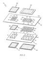
- FIG. 2 is an exploded isometric top view of the semiconductor power module of FIG. 1 ;
- FIG. 3 is an exploded isometric bottom view of the semiconductor power module of FIG. 1 ;
- FIG. 4 depicts the lower face of an upper flexible circuit leadframe of the semiconductor power module of FIG. 1 ;
- FIG. 5 depicts the lower face of a lower flexible circuit leadframe of the semiconductor power module of FIG. 1 ;
- FIG. 6 is an isometric bottom view of the semiconductor power module of FIG. 1 ;
- FIG. 7 is a top view of the semiconductor power module of FIG. 1 .
- the present invention is directed to a power electronics module including one or more power semiconductor devices such as transistors and diodes that have solderable active areas on their opposing faces.
- an insulated gate bipolar power transistor, or IGBT typically has a solderable collector terminal formed on one of its faces and solderable gate and emitter terminals formed on its opposite face.
- the invention is described herein in the context of a power transistor switch including an IGBT (or FET) and a free-wheeling or anti-parallel diode, but it will be appreciated that the invention is applicable in general to power electronics modules including different numbers and kinds of power semiconductor devices.
- the reference numeral 10 generally designates a semiconductor power module according to this invention designed for double-side cooling by upper and lower cold plates 12 and 14.
- the illustrated module 10 houses two semiconductor chips 16 and 18.
- the upper face 16a of chip 16 is thermally coupled to the upper cold plate 12 through a first upper ceramic substrate 20, and the upper face 18a of chip 18 is thermally coupled to upper cold plate 12 through a second upper ceramic substrate 22.
- the lower face 16b of chip 16 is thermally coupled to the lower cold plate 14 through a first lower ceramic substrate 24, and the lower face 18b of chip 18 is thermally coupled to lower cold plate 14 through a second lower ceramic substrate 26.
- An upper flexible circuit leadframe 28 is disposed intermediate the chips 16, 18 and the upper ceramic substrates 20, 22 for electrically accessing terminals formed on the upper faces 16a and 18a of chips 16 and 18.
- a lower flexible circuit leadframe 30 is disposed intermediate the chips 16, 18 and the lower ceramic substrates 24, 26 for electrically accessing terminals formed on the lower faces 16b and 18b of chips 16 and 18.
- the upper and lower flexible circuit leadframes 28 and 30 each comprise a patterned copper layer 28a and 30a sandwiched between a pair of patterned insulation layers 28b, 28c and 30b, 30c.
- chip 16 is an insulated-gate-bipolar-transistor (IGBT) and that chip 18 is a free-wheeling or anti-parallel diode.
- IGBT gate terminal 32 and a segmented array of IGBT emitter terminals 34 are formed on the upper face 16a of chip 16.
- the diode anode terminal 36 is formed on the upper face 18a of chip 18.
- the IGBT collector terminal 35 is formed on the lower face 16b of chip 16, and the diode cathode terminal 37 is formed on the lower face 18b of chip 18.
- the insulation layers 28b and 28c of upper flexible circuit leadframe 28 are patterned to provide an array of un-insulated regions 38, 40, 42 that correspond and register with the gate, emitter and anode terminals 32, 34 and 36. Additionally, the inboard insulation layer 28c is patterned to provide a set of three peripheral un-insulated regions 46, 48 and 50 for external access to the terminals 32, 34 and 36 via the exposed leadframe copper areas 52, 54 and 56 of copper layer 28a.
- An exposed leadframe copper pad 58 in the un-insulated region 38 is soldered to the gate terminal 32 of chip 16, and an insulated leg 60 of the copper layer 28a electrically joins the copper pad 58 to the exposed peripheral copper area 52, which serves as the gate terminal of the module 10.
- Exposed leadframe copper pads 62 in the un-insulated regions 40 are soldered to the emitter terminals 34 of chip 16, and exposed leadframe copper pads 64 in the un-insulated regions 42 are soldered to the anode terminal 36 of chip 18.
- An insulated portion 66 of the copper layer 28a electrically joins the copper pads 62 and 64 to the exposed peripheral copper areas 54 and 56.
- the insulated portion 66 of the copper layer 28a serves to electrically couple the emitter terminals 34 of chip 16 to the anode terminal 36 of chip 18, and to provide electrical access to the joined emitter and anode terminals 34, 36 at the peripheral copper areas 54 and 56, which serve as low voltage terminals for the module 10.
- the insulation layers 30b and 30c of lower flexible circuit leadframe 30 are patterned to provide an array of un-insulated regions 70 and 72 that correspond and register with the collector and cathode terminals 35 and 37 of chips 16 and 18. Additionally, the outboard insulation layer 30c is patterned to provide a set of two peripheral un-insulated regions 74 and 76 for external access to the terminals 35 and 37 via the exposed leadframe copper areas 78 and 80 of copper layer 30a. Exposed leadframe copper pads 82 in the un-insulated region 70 are soldered to the collector terminal 35 of chip 16, and exposed leadframe copper pads 84 in the un-insulated region 72 are soldered to the cathode terminal 37 of chip 18. As seen in FIG.
- an insulated portion 86 of the copper layer 30a electrically joins the copper pads 82 and 84 to the exposed peripheral copper areas 78 and 80.
- the insulated portion 86 of the copper layer 30a serves to electrically couple the collector terminal 35 of chip 16 to the cathode terminal 37 of chip 18, and to provide electrical access to the joined collector and cathode terminals 35, 37 at the peripheral copper areas 78 and 80, which serve as high voltage terminals for the module 10.
- the gate terminal 52 and emitter/anode terminals 54, 56 provided on upper flexible circuit leadframe 28 and the collector/cathode terminals 78, 80 provided on lower flexible circuit leadframe 30 are all accessible on the same (lower) side of module 10.
- the upper flexible circuit leadframe 28 extends laterally beyond the lower flexible circuit leadframe 30 so that the lower flexible circuit leadframe 30 does not cover the gate and emitter/anode terminals 52, 54, 56 of upper flexible circuit leadframe 28.
- terminals 52, 54, 56, 78, 80 may be variously arranged to accommodate the requirements of a given application, and the flexible nature of the leadframes 28, 30 allows the terminal portions to be bent out of the plane of the chips 16, 18 for connection to an external circuit board or bus bar, if desired.
- the outboard surfaces of the upper and lower ceramic substrates 20-26 are each clad with a metal layer (such as copper, aluminum, or any conventional thick film or thin film conductor formulation) to promote heat transfer from the module 10 to the upper and lower cold plates 12 and 14. Additionally, the inboard surfaces of the substrates 20-26 bear a metal cladding that is soldered to the chips 16, 18 and the flexible circuit leadframes 28, 30. Referring to FIG. 2-3 , for example, the inboard face of upper ceramic substrate 20 is clad with a metallization pattern that matches and registers with the gate and emitter terminals 32, 34 of chip 16.
- a metal layer such as copper, aluminum, or any conventional thick film or thin film conductor formulation
- the substrate's metallization pattern is soldered to the exposed copper pads 52 and 62 of upper flexible circuit leadframe 28, as well as the emitter terminals 34 of chip 16. And of course, the exposed copper pads 52 and 62 of leadframe 28 are soldered to the gate and emitter terminals 32 and 34 of chip 16. Corresponding solder joints are formed between each ceramic substrate 20-26 and the adjacent chip terminals and leadframe copper pads.
- the present invention provides an improved semiconductor power module leadframe arrangement.
- the disclosed leadframe arrangement offers numerous advantages when compared with conventional discrete metal leadframes.
- the use of selectively insulated flexible circuit leadframes ensures that all metal runners between soldered connections are electrically insulated from adjacent conductive components such as the cold plates 12 and 14.
- the flexible circuit leadframes and improved cooling allow the module 10 to be considerably thinner than a conventionally semiconductor power module.
- the module 10 is relatively inexpensive to produce as well because the overall ceramic substrate surface area is considerably reduced compared to a module in which multiple chips are soldered to the same substrate.
- using separate ceramic substrates for each chip of a multi-chip module enables the use of chips having different thicknesses.
Landscapes
- Cooling Or The Like Of Semiconductors Or Solid State Devices (AREA)
- Structures Or Materials For Encapsulating Or Coating Semiconductor Devices Or Solid State Devices (AREA)
Abstract
Description
- The present invention relates to a power module including at least one semiconductor chip, where the power module is clamped against a cold plate to dissipate heat generated by the chip, and more particularly to a power module having an improved leadframe arrangement for accessing electrical terminals of the chip.
- Semiconductor power modules house one or more semiconductor power devices such as transistors or diodes, and can be used as components of a power circuit such as a converter or inverter. Ordinarily, the electrical terminals of the chip are wire-bonded to a metal leadframe at the periphery of the chip, and the chip and leadframe can be sandwiched between a pair of ceramic substrates that dissipate heat generated by the chip. The modules are normally constructed as flat rectangular packages that can be clamped against a cold plate (or heat sink), or even sandwiched between a pair of cold plates for double-sided cooling. In the latter case particularly, it can be difficult to ensure that there will be adequate electrical insulation between the metal leadframe of the module and the adjacent cold plates, especially in high voltage applications. A related concern arises in connection with large semiconductor transistor chips such as IGBTs and FETs where the gate terminal is coupled to segmented emitter or source terminals by an array of exposed conductive links because of the close proximity of the metal leadframe to the gate terminal links. Accordingly, what is needed is an improved semiconductor power module leadframe arrangement that is adequately insulated against inadvertent electrical shorting.
- The present invention is directed to an improved semiconductor power module including a semiconductor chip thermally interfaced to a ceramic substrate for heat dissipation and a leadframe defined by a flexible circuit disposed intermediate the chip and the ceramic substrate. The flexible circuit comprises an inner conductor pattern that is selectively encased in an insulated jacket to ensure adequate electrical insulation between the leadframe conductor pattern and adjacent conductive surfaces. Preferably, the module is constructed for double side cooling by sandwiching the chip between a pair of ceramic substrates and providing intermediate flexible circuit leadframes on both sides of the chip for electrically accessing the chip terminals. In modules including two or more semiconductor chips, separate ceramic substrates are provided for each chip for low cost and to accommodate different chip thicknesses, and a single flexible circuit leadframe provides electrical interconnects to all of the chips.
-
FIG. 1 is an exploded side view of an actively or passively cooled semiconductor power module according to this invention; -
FIG. 2 is an exploded isometric top view of the semiconductor power module ofFIG. 1 ; -
FIG. 3 is an exploded isometric bottom view of the semiconductor power module ofFIG. 1 ; -
FIG. 4 depicts the lower face of an upper flexible circuit leadframe of the semiconductor power module ofFIG. 1 ; -
FIG. 5 depicts the lower face of a lower flexible circuit leadframe of the semiconductor power module ofFIG. 1 ; -
FIG. 6 is an isometric bottom view of the semiconductor power module ofFIG. 1 ; and -
FIG. 7 is a top view of the semiconductor power module ofFIG. 1 . - The present invention is directed to a power electronics module including one or more power semiconductor devices such as transistors and diodes that have solderable active areas on their opposing faces. For example, an insulated gate bipolar power transistor, or IGBT, typically has a solderable collector terminal formed on one of its faces and solderable gate and emitter terminals formed on its opposite face. The invention is described herein in the context of a power transistor switch including an IGBT (or FET) and a free-wheeling or anti-parallel diode, but it will be appreciated that the invention is applicable in general to power electronics modules including different numbers and kinds of power semiconductor devices.
- Referring to the drawings, and particularly to
FIG. 1 , thereference numeral 10 generally designates a semiconductor power module according to this invention designed for double-side cooling by upper and lowercold plates FIGS. 1-3 , the illustratedmodule 10 houses twosemiconductor chips upper face 16a ofchip 16 is thermally coupled to the uppercold plate 12 through a first upperceramic substrate 20, and theupper face 18a ofchip 18 is thermally coupled to uppercold plate 12 through a second upperceramic substrate 22. Similarly, thelower face 16b ofchip 16 is thermally coupled to the lowercold plate 14 through a first lowerceramic substrate 24, and the lower face 18b ofchip 18 is thermally coupled to lowercold plate 14 through a second lowerceramic substrate 26. An upperflexible circuit leadframe 28 is disposed intermediate thechips ceramic substrates upper faces chips flexible circuit leadframe 30 is disposed intermediate thechips ceramic substrates lower faces 16b and 18b ofchips FIG. 1 , the upper and lowerflexible circuit leadframes copper layer insulation layers - For purposes of discussion, it will be assumed that
chip 16 is an insulated-gate-bipolar-transistor (IGBT) and thatchip 18 is a free-wheeling or anti-parallel diode. Referring toFIG. 2 , theIGBT gate terminal 32 and a segmented array ofIGBT emitter terminals 34 are formed on theupper face 16a ofchip 16. Thediode anode terminal 36 is formed on theupper face 18a ofchip 18. Referring toFIG. 3 , theIGBT collector terminal 35 is formed on thelower face 16b ofchip 16, and thediode cathode terminal 37 is formed on the lower face 18b ofchip 18. - Referring to
FIGS. 2-3 and4 , theinsulation layers flexible circuit leadframe 28 are patterned to provide an array of un-insulatedregions anode terminals inboard insulation layer 28c is patterned to provide a set of threeperipheral un-insulated regions terminals leadframe copper areas copper layer 28a. An exposed leadframe copper pad 58 in theun-insulated region 38 is soldered to thegate terminal 32 ofchip 16, and an insulatedleg 60 of thecopper layer 28a electrically joins the copper pad 58 to the exposedperipheral copper area 52, which serves as the gate terminal of themodule 10. Exposedleadframe copper pads 62 in theun-insulated regions 40 are soldered to theemitter terminals 34 ofchip 16, and exposedleadframe copper pads 64 in theun-insulated regions 42 are soldered to theanode terminal 36 ofchip 18. Aninsulated portion 66 of thecopper layer 28a electrically joins thecopper pads peripheral copper areas portion 66 of thecopper layer 28a serves to electrically couple theemitter terminals 34 ofchip 16 to theanode terminal 36 ofchip 18, and to provide electrical access to the joined emitter andanode terminals peripheral copper areas module 10. - Referring to
FIGS. 2-3 and5 , theinsulation layers flexible circuit leadframe 30 are patterned to provide an array of un-insulatedregions cathode terminals chips outboard insulation layer 30c is patterned to provide a set of twoperipheral un-insulated regions terminals leadframe copper areas copper layer 30a. Exposedleadframe copper pads 82 in theun-insulated region 70 are soldered to thecollector terminal 35 ofchip 16, and exposedleadframe copper pads 84 in theun-insulated region 72 are soldered to thecathode terminal 37 ofchip 18. As seen inFIG. 5 , aninsulated portion 86 of thecopper layer 30a electrically joins thecopper pads peripheral copper areas insulated portion 86 of thecopper layer 30a serves to electrically couple thecollector terminal 35 ofchip 16 to thecathode terminal 37 ofchip 18, and to provide electrical access to the joined collector andcathode terminals peripheral copper areas module 10. - As best seen in
FIG. 6 , thegate terminal 52 and emitter/anode terminals flexible circuit leadframe 28 and the collector/cathode terminals flexible circuit leadframe 30 are all accessible on the same (lower) side ofmodule 10. The upperflexible circuit leadframe 28 extends laterally beyond the lowerflexible circuit leadframe 30 so that the lowerflexible circuit leadframe 30 does not cover the gate and emitter/anode terminals flexible circuit leadframe 28. Of course, theterminals leadframes chips - As seen in
FIGS. 2-3 and6-7 , the outboard surfaces of the upper and lower ceramic substrates 20-26 are each clad with a metal layer (such as copper, aluminum, or any conventional thick film or thin film conductor formulation) to promote heat transfer from themodule 10 to the upper and lowercold plates chips flexible circuit leadframes FIG. 2-3 , for example, the inboard face of upperceramic substrate 20 is clad with a metallization pattern that matches and registers with the gate andemitter terminals chip 16. The substrate's metallization pattern is soldered to the exposedcopper pads flexible circuit leadframe 28, as well as theemitter terminals 34 ofchip 16. And of course, the exposedcopper pads leadframe 28 are soldered to the gate andemitter terminals chip 16. Corresponding solder joints are formed between each ceramic substrate 20-26 and the adjacent chip terminals and leadframe copper pads. - In summary, the present invention provides an improved semiconductor power module leadframe arrangement. The disclosed leadframe arrangement offers numerous advantages when compared with conventional discrete metal leadframes. First, the use of selectively insulated flexible circuit leadframes ensures that all metal runners between soldered connections are electrically insulated from adjacent conductive components such as the
cold plates module 10 to be considerably thinner than a conventionally semiconductor power module. Themodule 10 is relatively inexpensive to produce as well because the overall ceramic substrate surface area is considerably reduced compared to a module in which multiple chips are soldered to the same substrate. In the same vein, using separate ceramic substrates for each chip of a multi-chip module enables the use of chips having different thicknesses. - While the present invention has been described in reference to the illustrated embodiment, it will be understood that numerous modifications and variations in addition to those mentioned above will occur to those skilled in the art. For example, the disclosed apparatus is applicable to modules housing a different number of chips, just one flexible circuit leadframe, and so on. Additionally, the flexible circuit terminals 54-56, 78-80 may be arranged to accommodate planar (i.e., non-pedestal)
cold plates
Claims (10)
- A semiconductor power module (10), comprising:a semiconductor chip (16) having a first face (16a) on which is formed a first active area (34);a first heat dissipative element (20) for dissipating heat generated by the semiconductor chip (16); anda first multi-layer flexible circuit leadframe (28) disposed between the first face (16a) of the semiconductor chip (16) and the first heat dissipative element (20), including a conductor layer (28a) sandwiched between a first pair of insulation layers (28b, 28c), the first pair of insulation layers (28b, 28c) being patterned to provide a first inner un-insulated region (62) of said conductor layer (28a) in registry with the first active area (34) of said semiconductor chip (16), and a first outer un-insulated region (54, 56) of said conductor layer (28a) that is disposed laterally outboard of said semiconductor chip (16) and said first heat dissipative element (20) for providing electrical access to the first active area (34) of said semiconductor chip (16).
- The semiconductor power module of claim 1, where:said first heat dissipative element (20) has a solderable surface facing said first multi-layer flexible circuit leadframe (28);said first inner un-insulated region (62) of said conductor layer (28a) is patterned to place a portion of the first active area (34) of said semiconductor chip (16) adjacent the solderable surface of said first heat dissipating element (20); andsaid portion of the first active area (34) of said semiconductor chip (16) is soldered to the solderable surface of said first heat dissipating element (20).
- The semiconductor power module of claim 2, where:said first inner un-insulated region (62) of said conductor layer (28a) is soldered to the first active area (34) of said semiconductor chip (16) and to the solderable surface of said first heat dissipative element (20).
- The semiconductor power module of claim 1, where:said first heat dissipative element (20) includes a ceramic substrate.
- The semiconductor power module of claim 1, where the semiconductor chip (16) has a second face (16b) on which is formed a second active area (35);
a second heat dissipative element (24) for dissipating heat generated by the semiconductor chip (16); and
a second multi-layer flexible circuit leadframe (30) disposed between the second face (16b) of the semiconductor chip (16) and the second heat dissipative element (24), including a conductor layer (30a) sandwiched between a second pair of insulation layers (30b, 30c), the insulation layers (30b, 30c) being patterned to provide a second inner un-insulated region (82) of said conductor layer (30a) in registry with the second active area (35) of said semiconductor chip (16), and a second outer un-insulated region (78, 80) of said conductor layer (30a) that is disposed laterally outboard of said semiconductor chip (16) and said second heat dissipative element (24) for providing electrical access to the second active area (35) of said semiconductor chip (16). - The semiconductor power module of claim 5, where:said second heat dissipative element (24) has a solderable surface facing said second multi-layer flexible circuit leadframe (30);said second inner un-insulated region (82) of said conductor layer (30a) is patterned to place a portion of the second active area (35) of said semiconductor chip (16) adjacent the solderable surface of said second heat dissipating element (24); andsaid portion of the second active area (35) of said semiconductor chip (16) is soldered to the solderable surface of said second heat dissipating element (24).
- The semiconductor power module of claim 6, where:said second inner un-insulated region (82) of said conductor layer (30a) is soldered to the second active area (35) of said semiconductor chip (16) and to the solderable surface of said second heat dissipative element (24).
- The semiconductor power module of claim 5, where:said second heat dissipative element (24) includes a ceramic substrate.
- A semiconductor power module, comprising:first and second semiconductor chips (16, 18), each having upper (16a, 18a) and lower (16b, 18b) opposing faces on which are formed electrical terminals (34, 36; 35, 37), and each being disposed between respective upper and lower heat dissipative elements (20, 24; 22, 26);an upper flexible circuit leadframe (28) disposed between the upper heat dissipative elements (20, 22) and the upper faces (16a, 18a) of the semiconductor chips (16, 18), the upper flexible circuit leadframe (28) including a selectively insulated conductor layer (28a) having un-insulated inner regions (62, 64) in registry with the electrical terminals (34, 36) formed on the upper faces (16a, 18a) of said semiconductor chips (16, 18), and un-insulated peripheral regions (48, 50) that are electrically linked to the un-insulated inner regions (62, 64) to provide electrical access to the electrical terminals (34, 36) formed on the upper faces (16a, 18a) of said semiconductor chips (16, 18); anda lower flexible circuit leadframe (30) disposed between the lower heat dissipative elements (24, 26) and the lower faces (16b, 18b) of the semiconductor chips (16, 18), the lower flexible circuit leadframe (30) including a selectively insulated conductor layer (30a) having un-insulated inner regions (82, 84) in registry with the electrical terminals (35, 37) formed on the lower faces (16b, 18b) of the semiconductor chips (16, 18), and un-insulated peripheral regions (78, 80) that are electrically linked to the un-insulated inner regions (82, 84) to provide electrical access to the electrical terminals (35, 37) formed on the lower faces (16b, 18b) of the semiconductor chips (16, 18).
- The semiconductor power module of Claim 9, where:the un-insulated inner regions (54, 56;76, 78) of said upper and lower flexible circuit leadframes (28, 30) are patterned to thermally couple the electrical terminals (34, 36; 35, 37) formed on the upper and lower faces (16a, 18a; 16b, 18b) of said semiconductor chips (16, 18) with respective upper and lower heat dissipating elements (20, 24; 22, 26).
Applications Claiming Priority (1)
| Application Number | Priority Date | Filing Date | Title |
|---|---|---|---|
| US11/899,365 US7960817B2 (en) | 2007-09-05 | 2007-09-05 | Semiconductor power module with flexible circuit leadframe |
Publications (2)
| Publication Number | Publication Date |
|---|---|
| EP2068362A1 true EP2068362A1 (en) | 2009-06-10 |
| EP2068362B1 EP2068362B1 (en) | 2011-04-20 |
Family
ID=40406111
Family Applications (1)
| Application Number | Title | Priority Date | Filing Date |
|---|---|---|---|
| EP08163295A Active EP2068362B1 (en) | 2007-09-05 | 2008-08-29 | Semiconductor power module with flexible circuit leadframe |
Country Status (4)
| Country | Link |
|---|---|
| US (1) | US7960817B2 (en) |
| EP (1) | EP2068362B1 (en) |
| AT (1) | ATE506699T1 (en) |
| DE (1) | DE602008006334D1 (en) |
Families Citing this family (8)
| Publication number | Priority date | Publication date | Assignee | Title |
|---|---|---|---|---|
| US8461623B2 (en) * | 2008-07-10 | 2013-06-11 | Mitsubishi Electric Corporation | Power semiconductor module |
| EP2270855A1 (en) * | 2009-06-29 | 2011-01-05 | ABB Research Ltd. | An electrical module |
| JP6165525B2 (en) | 2012-10-31 | 2017-07-19 | 株式会社東芝 | Semiconductor power conversion device and manufacturing method thereof |
| US9974187B2 (en) | 2013-04-22 | 2018-05-15 | Infineon Technologies Austria Ag | Power in lead |
| CA2978795A1 (en) | 2015-03-16 | 2016-09-22 | Dana Canada Corporation | Heat exchangers with plates having surface patterns for enhancing flatness and methods for manufacturing same |
| KR102603062B1 (en) * | 2016-12-15 | 2023-11-16 | 현대자동차주식회사 | Input terminal of power module of double-side cooling |
| WO2020212031A1 (en) | 2019-04-18 | 2020-10-22 | Abb Power Grids Switzerland Ag | Power semiconductor module with laser-welded leadframe |
| CN119673883B (en) * | 2024-12-03 | 2025-10-14 | 珠海格力电子元器件有限公司 | Intelligent Power Module |
Citations (2)
| Publication number | Priority date | Publication date | Assignee | Title |
|---|---|---|---|---|
| US4313262A (en) * | 1979-12-17 | 1982-02-02 | General Electric Company | Molybdenum substrate thick film circuit |
| EP0372228A1 (en) | 1988-11-09 | 1990-06-13 | Semikron Elektronik Gmbh | Semiconductor element comprising a carrier |
Family Cites Families (3)
| Publication number | Priority date | Publication date | Assignee | Title |
|---|---|---|---|---|
| DE19617055C1 (en) * | 1996-04-29 | 1997-06-26 | Semikron Elektronik Gmbh | High-density multilayer prepreg semiconductor power module |
| US6731002B2 (en) * | 2001-05-04 | 2004-05-04 | Ixys Corporation | High frequency power device with a plastic molded package and direct bonded substrate |
| US7423332B2 (en) * | 2003-08-26 | 2008-09-09 | Delphi Technologies, Inc. | Vertical laminated electrical switch circuit |
-
2007
- 2007-09-05 US US11/899,365 patent/US7960817B2/en active Active
-
2008
- 2008-08-29 AT AT08163295T patent/ATE506699T1/en not_active IP Right Cessation
- 2008-08-29 DE DE602008006334T patent/DE602008006334D1/en active Active
- 2008-08-29 EP EP08163295A patent/EP2068362B1/en active Active
Patent Citations (2)
| Publication number | Priority date | Publication date | Assignee | Title |
|---|---|---|---|---|
| US4313262A (en) * | 1979-12-17 | 1982-02-02 | General Electric Company | Molybdenum substrate thick film circuit |
| EP0372228A1 (en) | 1988-11-09 | 1990-06-13 | Semikron Elektronik Gmbh | Semiconductor element comprising a carrier |
Also Published As
| Publication number | Publication date |
|---|---|
| DE602008006334D1 (en) | 2011-06-01 |
| EP2068362B1 (en) | 2011-04-20 |
| US7960817B2 (en) | 2011-06-14 |
| US20090057853A1 (en) | 2009-03-05 |
| ATE506699T1 (en) | 2011-05-15 |
Similar Documents
| Publication | Publication Date | Title |
|---|---|---|
| US6946740B2 (en) | High power MCM package | |
| US7834448B2 (en) | Fluid cooled semiconductor power module having double-sided cooling | |
| EP2068362B1 (en) | Semiconductor power module with flexible circuit leadframe | |
| US7045884B2 (en) | Semiconductor device package | |
| US20070236883A1 (en) | Electronics assembly having heat sink substrate disposed in cooling vessel | |
| US6943293B1 (en) | High power electronic package with enhanced cooling characteristics | |
| US12400930B2 (en) | Power module package | |
| US11456244B2 (en) | Semiconductor device | |
| CN111261598A (en) | Packaging structure and power module applicable to same | |
| US20250311175A1 (en) | Metal substrate heat dissipation structure and photovoltaic power optimizer | |
| US12489031B2 (en) | Semiconductor device and manufacturing method thereof | |
| US12133366B2 (en) | Power electronics module with improved cooling | |
| CN105051898A (en) | Semiconductor devices | |
| CN117528898A (en) | Circuit boards and electronic equipment | |
| JP7163583B2 (en) | semiconductor equipment | |
| TWI244182B (en) | Heat-dissipation device | |
| CN113745203A (en) | Semiconductor module | |
| JP3855726B2 (en) | Power module | |
| US20250192061A1 (en) | Semiconductor Module and Power Conversion Device | |
| US11990391B2 (en) | Semiconductor device | |
| CN110634813A (en) | Package structure | |
| JP2006066464A (en) | Semiconductor device | |
| WO2022059052A1 (en) | Power semiconductor module | |
| JP2003298009A (en) | Power module and power conversion device using the same | |
| WO2025027902A1 (en) | Semiconductor device |
Legal Events
| Date | Code | Title | Description |
|---|---|---|---|
| PUAI | Public reference made under article 153(3) epc to a published international application that has entered the european phase |
Free format text: ORIGINAL CODE: 0009012 |
|
| AK | Designated contracting states |
Kind code of ref document: A1 Designated state(s): AT BE BG CH CY CZ DE DK EE ES FI FR GB GR HR HU IE IS IT LI LT LU LV MC MT NL NO PL PT RO SE SI SK TR |
|
| AX | Request for extension of the european patent |
Extension state: AL BA MK RS |
|
| 17P | Request for examination filed |
Effective date: 20091210 |
|
| 17Q | First examination report despatched |
Effective date: 20100113 |
|
| AKX | Designation fees paid |
Designated state(s): AT BE BG CH CY CZ DE DK EE ES FI FR GB GR HR HU IE IS IT LI LT LU LV MC MT NL NO PL PT RO SE SI SK TR |
|
| GRAP | Despatch of communication of intention to grant a patent |
Free format text: ORIGINAL CODE: EPIDOSNIGR1 |
|
| GRAS | Grant fee paid |
Free format text: ORIGINAL CODE: EPIDOSNIGR3 |
|
| GRAA | (expected) grant |
Free format text: ORIGINAL CODE: 0009210 |
|
| AK | Designated contracting states |
Kind code of ref document: B1 Designated state(s): AT BE BG CH CY CZ DE DK EE ES FI FR GB GR HR HU IE IS IT LI LT LU LV MC MT NL NO PL PT RO SE SI SK TR |
|
| REG | Reference to a national code |
Ref country code: GB Ref legal event code: FG4D |
|
| REG | Reference to a national code |
Ref country code: CH Ref legal event code: EP |
|
| REG | Reference to a national code |
Ref country code: IE Ref legal event code: FG4D |
|
| REF | Corresponds to: |
Ref document number: 602008006334 Country of ref document: DE Date of ref document: 20110601 Kind code of ref document: P |
|
| REG | Reference to a national code |
Ref country code: DE Ref legal event code: R096 Ref document number: 602008006334 Country of ref document: DE Effective date: 20110601 |
|
| REG | Reference to a national code |
Ref country code: NL Ref legal event code: VDEP Effective date: 20110420 |
|
| LTIE | Lt: invalidation of european patent or patent extension |
Effective date: 20110420 |
|
| PG25 | Lapsed in a contracting state [announced via postgrant information from national office to epo] |
Ref country code: HR Free format text: LAPSE BECAUSE OF FAILURE TO SUBMIT A TRANSLATION OF THE DESCRIPTION OR TO PAY THE FEE WITHIN THE PRESCRIBED TIME-LIMIT Effective date: 20110420 Ref country code: PT Free format text: LAPSE BECAUSE OF FAILURE TO SUBMIT A TRANSLATION OF THE DESCRIPTION OR TO PAY THE FEE WITHIN THE PRESCRIBED TIME-LIMIT Effective date: 20110822 Ref country code: SE Free format text: LAPSE BECAUSE OF FAILURE TO SUBMIT A TRANSLATION OF THE DESCRIPTION OR TO PAY THE FEE WITHIN THE PRESCRIBED TIME-LIMIT Effective date: 20110420 Ref country code: LT Free format text: LAPSE BECAUSE OF FAILURE TO SUBMIT A TRANSLATION OF THE DESCRIPTION OR TO PAY THE FEE WITHIN THE PRESCRIBED TIME-LIMIT Effective date: 20110420 Ref country code: NO Free format text: LAPSE BECAUSE OF FAILURE TO SUBMIT A TRANSLATION OF THE DESCRIPTION OR TO PAY THE FEE WITHIN THE PRESCRIBED TIME-LIMIT Effective date: 20110720 |
|
| REG | Reference to a national code |
Ref country code: DE Ref legal event code: R082 Ref document number: 602008006334 Country of ref document: DE |
|
| PG25 | Lapsed in a contracting state [announced via postgrant information from national office to epo] |
Ref country code: IS Free format text: LAPSE BECAUSE OF FAILURE TO SUBMIT A TRANSLATION OF THE DESCRIPTION OR TO PAY THE FEE WITHIN THE PRESCRIBED TIME-LIMIT Effective date: 20110820 Ref country code: CY Free format text: LAPSE BECAUSE OF FAILURE TO SUBMIT A TRANSLATION OF THE DESCRIPTION OR TO PAY THE FEE WITHIN THE PRESCRIBED TIME-LIMIT Effective date: 20110420 Ref country code: SI Free format text: LAPSE BECAUSE OF FAILURE TO SUBMIT A TRANSLATION OF THE DESCRIPTION OR TO PAY THE FEE WITHIN THE PRESCRIBED TIME-LIMIT Effective date: 20110420 Ref country code: GR Free format text: LAPSE BECAUSE OF FAILURE TO SUBMIT A TRANSLATION OF THE DESCRIPTION OR TO PAY THE FEE WITHIN THE PRESCRIBED TIME-LIMIT Effective date: 20110721 Ref country code: BE Free format text: LAPSE BECAUSE OF FAILURE TO SUBMIT A TRANSLATION OF THE DESCRIPTION OR TO PAY THE FEE WITHIN THE PRESCRIBED TIME-LIMIT Effective date: 20110420 Ref country code: ES Free format text: LAPSE BECAUSE OF FAILURE TO SUBMIT A TRANSLATION OF THE DESCRIPTION OR TO PAY THE FEE WITHIN THE PRESCRIBED TIME-LIMIT Effective date: 20110731 Ref country code: LV Free format text: LAPSE BECAUSE OF FAILURE TO SUBMIT A TRANSLATION OF THE DESCRIPTION OR TO PAY THE FEE WITHIN THE PRESCRIBED TIME-LIMIT Effective date: 20110420 Ref country code: AT Free format text: LAPSE BECAUSE OF FAILURE TO SUBMIT A TRANSLATION OF THE DESCRIPTION OR TO PAY THE FEE WITHIN THE PRESCRIBED TIME-LIMIT Effective date: 20110420 Ref country code: FI Free format text: LAPSE BECAUSE OF FAILURE TO SUBMIT A TRANSLATION OF THE DESCRIPTION OR TO PAY THE FEE WITHIN THE PRESCRIBED TIME-LIMIT Effective date: 20110420 |
|
| PG25 | Lapsed in a contracting state [announced via postgrant information from national office to epo] |
Ref country code: NL Free format text: LAPSE BECAUSE OF FAILURE TO SUBMIT A TRANSLATION OF THE DESCRIPTION OR TO PAY THE FEE WITHIN THE PRESCRIBED TIME-LIMIT Effective date: 20110420 Ref country code: MT Free format text: LAPSE BECAUSE OF FAILURE TO SUBMIT A TRANSLATION OF THE DESCRIPTION OR TO PAY THE FEE WITHIN THE PRESCRIBED TIME-LIMIT Effective date: 20110420 |
|
| PG25 | Lapsed in a contracting state [announced via postgrant information from national office to epo] |
Ref country code: EE Free format text: LAPSE BECAUSE OF FAILURE TO SUBMIT A TRANSLATION OF THE DESCRIPTION OR TO PAY THE FEE WITHIN THE PRESCRIBED TIME-LIMIT Effective date: 20110420 Ref country code: CZ Free format text: LAPSE BECAUSE OF FAILURE TO SUBMIT A TRANSLATION OF THE DESCRIPTION OR TO PAY THE FEE WITHIN THE PRESCRIBED TIME-LIMIT Effective date: 20110420 |
|
| PLBE | No opposition filed within time limit |
Free format text: ORIGINAL CODE: 0009261 |
|
| STAA | Information on the status of an ep patent application or granted ep patent |
Free format text: STATUS: NO OPPOSITION FILED WITHIN TIME LIMIT |
|
| PG25 | Lapsed in a contracting state [announced via postgrant information from national office to epo] |
Ref country code: SK Free format text: LAPSE BECAUSE OF FAILURE TO SUBMIT A TRANSLATION OF THE DESCRIPTION OR TO PAY THE FEE WITHIN THE PRESCRIBED TIME-LIMIT Effective date: 20110420 Ref country code: PL Free format text: LAPSE BECAUSE OF FAILURE TO SUBMIT A TRANSLATION OF THE DESCRIPTION OR TO PAY THE FEE WITHIN THE PRESCRIBED TIME-LIMIT Effective date: 20110420 Ref country code: RO Free format text: LAPSE BECAUSE OF FAILURE TO SUBMIT A TRANSLATION OF THE DESCRIPTION OR TO PAY THE FEE WITHIN THE PRESCRIBED TIME-LIMIT Effective date: 20110420 Ref country code: DK Free format text: LAPSE BECAUSE OF FAILURE TO SUBMIT A TRANSLATION OF THE DESCRIPTION OR TO PAY THE FEE WITHIN THE PRESCRIBED TIME-LIMIT Effective date: 20110420 |
|
| 26N | No opposition filed |
Effective date: 20120123 |
|
| PG25 | Lapsed in a contracting state [announced via postgrant information from national office to epo] |
Ref country code: MC Free format text: LAPSE BECAUSE OF NON-PAYMENT OF DUE FEES Effective date: 20110831 |
|
| REG | Reference to a national code |
Ref country code: DE Ref legal event code: R097 Ref document number: 602008006334 Country of ref document: DE Effective date: 20120123 |
|
| REG | Reference to a national code |
Ref country code: IE Ref legal event code: MM4A |
|
| PG25 | Lapsed in a contracting state [announced via postgrant information from national office to epo] |
Ref country code: IE Free format text: LAPSE BECAUSE OF NON-PAYMENT OF DUE FEES Effective date: 20110829 |
|
| REG | Reference to a national code |
Ref country code: CH Ref legal event code: PL |
|
| PG25 | Lapsed in a contracting state [announced via postgrant information from national office to epo] |
Ref country code: CH Free format text: LAPSE BECAUSE OF NON-PAYMENT OF DUE FEES Effective date: 20120831 Ref country code: LI Free format text: LAPSE BECAUSE OF NON-PAYMENT OF DUE FEES Effective date: 20120831 |
|
| PG25 | Lapsed in a contracting state [announced via postgrant information from national office to epo] |
Ref country code: LU Free format text: LAPSE BECAUSE OF NON-PAYMENT OF DUE FEES Effective date: 20110829 |
|
| PG25 | Lapsed in a contracting state [announced via postgrant information from national office to epo] |
Ref country code: BG Free format text: LAPSE BECAUSE OF FAILURE TO SUBMIT A TRANSLATION OF THE DESCRIPTION OR TO PAY THE FEE WITHIN THE PRESCRIBED TIME-LIMIT Effective date: 20110720 |
|
| PG25 | Lapsed in a contracting state [announced via postgrant information from national office to epo] |
Ref country code: TR Free format text: LAPSE BECAUSE OF FAILURE TO SUBMIT A TRANSLATION OF THE DESCRIPTION OR TO PAY THE FEE WITHIN THE PRESCRIBED TIME-LIMIT Effective date: 20110420 |
|
| PG25 | Lapsed in a contracting state [announced via postgrant information from national office to epo] |
Ref country code: HU Free format text: LAPSE BECAUSE OF FAILURE TO SUBMIT A TRANSLATION OF THE DESCRIPTION OR TO PAY THE FEE WITHIN THE PRESCRIBED TIME-LIMIT Effective date: 20110420 |
|
| REG | Reference to a national code |
Ref country code: FR Ref legal event code: PLFP Year of fee payment: 9 |
|
| REG | Reference to a national code |
Ref country code: FR Ref legal event code: PLFP Year of fee payment: 10 |
|
| REG | Reference to a national code |
Ref country code: FR Ref legal event code: PLFP Year of fee payment: 11 |
|
| REG | Reference to a national code |
Ref country code: DE Ref legal event code: R081 Ref document number: 602008006334 Country of ref document: DE Owner name: DELPHI TECHNOLOGIES IP LIMITED, BB Free format text: FORMER OWNER: DELPHI TECHNOLOGIES, INC., MICHIGAN, US |
|
| REG | Reference to a national code |
Ref country code: GB Ref legal event code: 732E Free format text: REGISTERED BETWEEN 20190214 AND 20190221 |
|
| P01 | Opt-out of the competence of the unified patent court (upc) registered |
Effective date: 20230327 |
|
| REG | Reference to a national code |
Ref country code: DE Ref legal event code: R079 Ref document number: 602008006334 Country of ref document: DE Free format text: PREVIOUS MAIN CLASS: H01L0025070000 Ipc: H10D0080200000 |
|
| PGFP | Annual fee paid to national office [announced via postgrant information from national office to epo] |
Ref country code: DE Payment date: 20250709 Year of fee payment: 18 |
|
| PGFP | Annual fee paid to national office [announced via postgrant information from national office to epo] |
Ref country code: IT Payment date: 20250811 Year of fee payment: 18 |
|
| PGFP | Annual fee paid to national office [announced via postgrant information from national office to epo] |
Ref country code: GB Payment date: 20250710 Year of fee payment: 18 |
|
| PGFP | Annual fee paid to national office [announced via postgrant information from national office to epo] |
Ref country code: FR Payment date: 20250709 Year of fee payment: 18 |