EP2066157A2 - Wiring substrate and manufacturing method thereof - Google Patents
Wiring substrate and manufacturing method thereof Download PDFInfo
- Publication number
- EP2066157A2 EP2066157A2 EP08170158A EP08170158A EP2066157A2 EP 2066157 A2 EP2066157 A2 EP 2066157A2 EP 08170158 A EP08170158 A EP 08170158A EP 08170158 A EP08170158 A EP 08170158A EP 2066157 A2 EP2066157 A2 EP 2066157A2
- Authority
- EP
- European Patent Office
- Prior art keywords
- wiring
- insulating layer
- wiring substrate
- layer
- reinforcing body
- Prior art date
- Legal status (The legal status is an assumption and is not a legal conclusion. Google has not performed a legal analysis and makes no representation as to the accuracy of the status listed.)
- Withdrawn
Links
Images



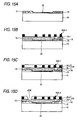


Classifications
-
- H—ELECTRICITY
- H05—ELECTRIC TECHNIQUES NOT OTHERWISE PROVIDED FOR
- H05K—PRINTED CIRCUITS; CASINGS OR CONSTRUCTIONAL DETAILS OF ELECTRIC APPARATUS; MANUFACTURE OF ASSEMBLAGES OF ELECTRICAL COMPONENTS
- H05K1/00—Printed circuits
- H05K1/02—Details
-
- H—ELECTRICITY
- H05—ELECTRIC TECHNIQUES NOT OTHERWISE PROVIDED FOR
- H05K—PRINTED CIRCUITS; CASINGS OR CONSTRUCTIONAL DETAILS OF ELECTRIC APPARATUS; MANUFACTURE OF ASSEMBLAGES OF ELECTRICAL COMPONENTS
- H05K1/00—Printed circuits
- H05K1/02—Details
- H05K1/0271—Arrangements for reducing stress or warp in rigid printed circuit boards, e.g. caused by loads, vibrations or differences in thermal expansion
-
- H—ELECTRICITY
- H05—ELECTRIC TECHNIQUES NOT OTHERWISE PROVIDED FOR
- H05K—PRINTED CIRCUITS; CASINGS OR CONSTRUCTIONAL DETAILS OF ELECTRIC APPARATUS; MANUFACTURE OF ASSEMBLAGES OF ELECTRICAL COMPONENTS
- H05K3/00—Apparatus or processes for manufacturing printed circuits
- H05K3/22—Secondary treatment of printed circuits
- H05K3/24—Reinforcing of the conductive pattern
-
- H—ELECTRICITY
- H10—SEMICONDUCTOR DEVICES; ELECTRIC SOLID-STATE DEVICES NOT OTHERWISE PROVIDED FOR
- H10W—GENERIC PACKAGES, INTERCONNECTIONS, CONNECTORS OR OTHER CONSTRUCTIONAL DETAILS OF DEVICES COVERED BY CLASS H10
- H10W42/00—Arrangements for protection of devices
- H10W42/121—Arrangements for protection of devices protecting against mechanical damage
-
- H—ELECTRICITY
- H10—SEMICONDUCTOR DEVICES; ELECTRIC SOLID-STATE DEVICES NOT OTHERWISE PROVIDED FOR
- H10W—GENERIC PACKAGES, INTERCONNECTIONS, CONNECTORS OR OTHER CONSTRUCTIONAL DETAILS OF DEVICES COVERED BY CLASS H10
- H10W70/00—Package substrates; Interposers; Redistribution layers [RDL]
- H10W70/60—Insulating or insulated package substrates; Interposers; Redistribution layers
- H10W70/62—Insulating or insulated package substrates; Interposers; Redistribution layers characterised by their interconnections
- H10W70/65—Shapes or dispositions of interconnections
-
- H—ELECTRICITY
- H10—SEMICONDUCTOR DEVICES; ELECTRIC SOLID-STATE DEVICES NOT OTHERWISE PROVIDED FOR
- H10W—GENERIC PACKAGES, INTERCONNECTIONS, CONNECTORS OR OTHER CONSTRUCTIONAL DETAILS OF DEVICES COVERED BY CLASS H10
- H10W90/00—Package configurations
- H10W90/401—Package configurations characterised by multiple insulating or insulated package substrates, interposers or RDLs
-
- H—ELECTRICITY
- H05—ELECTRIC TECHNIQUES NOT OTHERWISE PROVIDED FOR
- H05K—PRINTED CIRCUITS; CASINGS OR CONSTRUCTIONAL DETAILS OF ELECTRIC APPARATUS; MANUFACTURE OF ASSEMBLAGES OF ELECTRICAL COMPONENTS
- H05K2201/00—Indexing scheme relating to printed circuits covered by H05K1/00
- H05K2201/09—Shape and layout
- H05K2201/09209—Shape and layout details of conductors
- H05K2201/09654—Shape and layout details of conductors covering at least two types of conductors provided for in H05K2201/09218 - H05K2201/095
- H05K2201/09781—Dummy conductors, i.e. not used for normal transport of current; Dummy electrodes of components
-
- H—ELECTRICITY
- H05—ELECTRIC TECHNIQUES NOT OTHERWISE PROVIDED FOR
- H05K—PRINTED CIRCUITS; CASINGS OR CONSTRUCTIONAL DETAILS OF ELECTRIC APPARATUS; MANUFACTURE OF ASSEMBLAGES OF ELECTRICAL COMPONENTS
- H05K2201/00—Indexing scheme relating to printed circuits covered by H05K1/00
- H05K2201/10—Details of components or other objects attached to or integrated in a printed circuit board
- H05K2201/10613—Details of electrical connections of non-printed components, e.g. special leads
- H05K2201/10621—Components characterised by their electrical contacts
- H05K2201/10674—Flip chip
-
- H—ELECTRICITY
- H05—ELECTRIC TECHNIQUES NOT OTHERWISE PROVIDED FOR
- H05K—PRINTED CIRCUITS; CASINGS OR CONSTRUCTIONAL DETAILS OF ELECTRIC APPARATUS; MANUFACTURE OF ASSEMBLAGES OF ELECTRICAL COMPONENTS
- H05K2201/00—Indexing scheme relating to printed circuits covered by H05K1/00
- H05K2201/20—Details of printed circuits not provided for in H05K2201/01 - H05K2201/10
- H05K2201/2009—Reinforced areas, e.g. for a specific part of a flexible printed circuit
-
- H—ELECTRICITY
- H05—ELECTRIC TECHNIQUES NOT OTHERWISE PROVIDED FOR
- H05K—PRINTED CIRCUITS; CASINGS OR CONSTRUCTIONAL DETAILS OF ELECTRIC APPARATUS; MANUFACTURE OF ASSEMBLAGES OF ELECTRICAL COMPONENTS
- H05K3/00—Apparatus or processes for manufacturing printed circuits
- H05K3/10—Apparatus or processes for manufacturing printed circuits in which conductive material is applied to the insulating support in such a manner as to form the desired conductive pattern
- H05K3/20—Apparatus or processes for manufacturing printed circuits in which conductive material is applied to the insulating support in such a manner as to form the desired conductive pattern by affixing prefabricated conductor pattern
-
- H—ELECTRICITY
- H05—ELECTRIC TECHNIQUES NOT OTHERWISE PROVIDED FOR
- H05K—PRINTED CIRCUITS; CASINGS OR CONSTRUCTIONAL DETAILS OF ELECTRIC APPARATUS; MANUFACTURE OF ASSEMBLAGES OF ELECTRICAL COMPONENTS
- H05K3/00—Apparatus or processes for manufacturing printed circuits
- H05K3/10—Apparatus or processes for manufacturing printed circuits in which conductive material is applied to the insulating support in such a manner as to form the desired conductive pattern
- H05K3/20—Apparatus or processes for manufacturing printed circuits in which conductive material is applied to the insulating support in such a manner as to form the desired conductive pattern by affixing prefabricated conductor pattern
- H05K3/205—Apparatus or processes for manufacturing printed circuits in which conductive material is applied to the insulating support in such a manner as to form the desired conductive pattern by affixing prefabricated conductor pattern using a pattern electroplated or electroformed on a metallic carrier
-
- H—ELECTRICITY
- H05—ELECTRIC TECHNIQUES NOT OTHERWISE PROVIDED FOR
- H05K—PRINTED CIRCUITS; CASINGS OR CONSTRUCTIONAL DETAILS OF ELECTRIC APPARATUS; MANUFACTURE OF ASSEMBLAGES OF ELECTRICAL COMPONENTS
- H05K3/00—Apparatus or processes for manufacturing printed circuits
- H05K3/46—Manufacturing multilayer circuits
- H05K3/4602—Manufacturing multilayer circuits characterized by a special circuit board as base or central core whereon additional circuit layers are built or additional circuit boards are laminated
-
- H—ELECTRICITY
- H05—ELECTRIC TECHNIQUES NOT OTHERWISE PROVIDED FOR
- H05K—PRINTED CIRCUITS; CASINGS OR CONSTRUCTIONAL DETAILS OF ELECTRIC APPARATUS; MANUFACTURE OF ASSEMBLAGES OF ELECTRICAL COMPONENTS
- H05K3/00—Apparatus or processes for manufacturing printed circuits
- H05K3/46—Manufacturing multilayer circuits
- H05K3/4644—Manufacturing multilayer circuits by building the multilayer layer by layer, i.e. build-up multilayer circuits
-
- H—ELECTRICITY
- H10—SEMICONDUCTOR DEVICES; ELECTRIC SOLID-STATE DEVICES NOT OTHERWISE PROVIDED FOR
- H10P—GENERIC PROCESSES OR APPARATUS FOR THE MANUFACTURE OR TREATMENT OF DEVICES COVERED BY CLASS H10
- H10P72/00—Handling or holding of wafers, substrates or devices during manufacture or treatment thereof
- H10P72/70—Handling or holding of wafers, substrates or devices during manufacture or treatment thereof for supporting or gripping
- H10P72/74—Handling or holding of wafers, substrates or devices during manufacture or treatment thereof for supporting or gripping using temporarily an auxiliary support
- H10P72/7424—Handling or holding of wafers, substrates or devices during manufacture or treatment thereof for supporting or gripping using temporarily an auxiliary support used as a support during the manufacture of self-supporting substrates
Definitions
- the present invention relates to a wiring substrate and a manufacturing method thereof.
- a wiring substrate made by disposing a reinforcing member in a wiring member formed by removing a support body after a wiring layer and an insulating layer are layered on the support body and a manufacturing method of the wiring substrate.
- a method for manufacturing a wiring substrate in which an electronic component is mounted includes a method for obtaining a wiring substrate by separating a wiring layer from a support body after a necessary wiring layer is formed in a state capable of being peeled on the support body.
- the manufacturing method of the wiring substrate of this kind there is the support body at the time of forming a build-up wiring layer, so that the build-up wiring layer can surely be formed with high accuracy. Also, after the build-up wiring layer is formed, the support body is removed, so that improvement in electrical characteristics and thinning of the wiring substrate manufactured can be achieved.
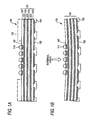
- FIG. 1(A) shows one example of a wiring substrate manufactured by this manufacturing method.
- a wiring substrate 100 shown in Fig. 1(A) is constructed so that a wiring member 101 is formed by layering wiring layers 102 and insulating layers 103 and upper electrode pads 107 are formed on an upper part of the wiring member and also lower electrode pads 108 are formed on a lower part of the wiring member. Also, it is constructed so that solder bumps 110 are formed on the upper electrode pads 107 and also the lower electrode pads 108 are exposed from a solder resist 109 formed on a lower surface of the wiring member 101.
- the wiring substrate 100 in which a support body is completely removed has a small mechanical strength of the substrate itself. Hence, there is a problem of easily deforming the wiring substrate 100 when external force is applied as shown in Fig. 1(B) .
- the invention has been implemented in view of the problems described above, and an object of the invention is to provide a wiring substrate capable of improving a mechanical strength while achieving thinning, and a manufacturing method of the wiring substrate.
- the wiring substrate according to independent claim 1 the manufacturing method according to independent claim 5, and the manufacturing method of claim 6 are provided. Further advantages, features, aspects and details are evident from the dependent claims, the description and the drawings.
- a wiring substrate including:
- the wiring substrate as in the first aspect, wherein the reinforcing body is arranged in a center position with respect to a thickness direction of the wiring member.
- the wiring substrate as in the first aspect, wherein the reinforcing bodies are arranged with space upward and downward across a center position with respect to a thickness direction of the wiring member.
- the wiring substrate as in any one of the first to third aspects, wherein the reinforcing body has a shape selected from at least a cross shape, an asterisk shape and a mesh shape in plan view.
- a manufacturing method of a wiring substrate including the steps of: arranging a protective member in a reinforcing body configured to cross plural linear members,
- a manufacturing method of a wiring substrate including the steps of:
- a seventh aspect of the invention there is provided the manufacturing method of a wiring substrate as in the sixth aspect, wherein the step of disposing the reinforcing body is performed plural times during formation of the wiring member, namely, after at least the wiring layer or the insulating layer is formed on the support body.
- the manufacturing method of a wiring substrate as in the sixth aspect wherein the step of disposing the reinforcing body is performed one time in a case of forming the wiring member to half of the predetermined thickness during formation of the wiring member, namely, after at least the wiring layer or the insulating layer is formed on the support body.
- the manufacturing method of a wiring substrate as in any one of the sixth to eighth aspects, wherein the reinforcing body is provided on the insulating layer in the step of disposing the reinforcing body.
- the step of disposing the reinforcing body includes processing for forming the reinforcing body on the insulating layer using a plating method.
- a reinforcing body configured to cross plural linear members between the insulating layers of a wiring member, even when stress or external force is applied to a wiring substrate from various directions, the plural linear members subjected to the stress etc. are configured to be crossed, so that the stress etc. from all directions can be reduced. Also, weight reduction in the wiring substrate can be achieved as compared with a conventional flat plate-shaped reinforcing body.
- An embodiment of the invention may be directed to a wiring substrate having a wiring member made by layering insulating layers and wiring layers, and a reinforcing body disposed between the insulating layers of this wiring member, this reinforcing body is configured to cross plural linear members.
- Embodiments are also directed to apparatuses for carrying out the disclosed methods and including apparatus parts for performing described method steps. Furthermore, embodiments are also directed to methods by which the described apparatus operates or by which the described apparatus is manufactured. It may include method steps for carrying out functions of the apparatus or manufacturing parts of the apparatus. The method steps may be performed by way of hardware components, firmware, software, a computer programmed by appropriate software, by any combination thereof or in any other manner.
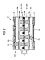
- Figs. 2 and 3 show a wiring substrate 1A which is a first embodiment of the invention.
- Fig. 2 is a partially sectional view of the wiring substrate 1A
- Fig. 3 shows a state of viewing the wiring substrate 1A from the plane.
- the wiring substrate 1A is broadly constructed of a wiring member 30A and a reinforcing body 50A.
- This wiring substrate 1A has a rectangular shape in which, for example, a length L1 (shown by an arrow in Fig. 3 ) of one side is 30 mm to 50 mm in plan view.
- a semiconductor chip 11 (only the outline is shown in Fig. 3 ) is mounted in this wiring substrate 1A.
- the wiring member 30A is constructed of a base body 17, a second wiring layer 18a, a third wiring layer 18b and solder resists 21, 22, etc.
- the base body 17 is disposed in substantially the center position of the wiring member 30A.
- This base body 17 is constructed of a base half body 17a located upward and a base half body 17b located downward.
- the base half body 17a is constructed of an insulating layer half body 20-1 formed by a resin material such as an epoxy resin or a polyimide resin, the second wiring layer 18a and a first wiring layer 18 formed in this insulating layer half body 20-1.
- the first wiring layer 18 is formed in a position of bonding between the base half body 17a and the base half body 17b.
- the second wiring layer 18a is constructed of a wiring part and a via part, and the via part is configured to be connected to the first wiring layer 18.
- the base half body 17b is constructed of an insulating layer half body 20-2 formed by a resin material such as an epoxy resin or a polyimide resin and the second wiring layer 18a formed in this insulating layer half body 20-2.
- This second wiring layer 18a is constructed of a wiring part and a via part, and the via part is configured to be connected to the first wiring layer 18. Therefore, the second wiring layer 18a formed in the base half body 17a is configured to be electrically connected to the second wiring layer 18a formed in the base half body 17b through the first wiring layer 18.
- a second insulating layer 20a, the third wiring layer 18b and the solder resists 21, 22, etc. are configured to be arranged in an upper part and a lower part of the base body 17 configured above.
- the second insulating layer 20a is formed by a resin material such as an epoxy resin or a polyimide resin and also, the third wiring layer 18b is formed by Cu (copper).
- This second insulating layer 20a and the third wiring layer 18b are respectively formed on both of upper and lower surfaces of the base body 17 using a build-up method as described below.
- the solder resists 21, 22 cover the front of the wiring member 30A excluding the portion used as an external connection terminal of the third wiring layer 18b. Also, pad surface plated layers 25, 26 are formed in the portion exposed from the solder resist 22 of the third wiring layer 18b.
- the pad surface plated layers 25, 26 have a structure layered by being plated with Ni (nickel) and Au (gold).
- the reinforcing body 50A is arranged in substantially the center position with respect to a thickness direction of the wiring member 30A. Concretely, the reinforcing body 50A is arranged in a state of being sandwiched between a pair of the insulating layer half bodies 20-1, 20-2 in a position of the boundary between the base half body 17a and the base half body 17b of the inside of the base body 17.
- This reinforcing body 50A is configured to cross plural linear members 51A with straight line shapes and have a mesh shape as a whole as shown in Fig. 3 .
- a width W1 and a height H (see Fig. 4 for the height H) of each of the linear members 51A can be selected in the range of 50 ⁇ m to 400 ⁇ m, and are preferably set at 100 ⁇ m in its range.
- a pitch P between the adjacent linear members 51A can be selected in the range of 200 ⁇ m to 800 ⁇ m, and is preferably set at 500 ⁇ m in its range.
- the reinforcing body 50A is shown as a uniform mesh structure, but a mesh shape is properly deformed so as not to interfere with the first and second wiring layers 18, 18a.
- the reinforcing body 50A is subjected to this stress or external force, and these forces are not applied to the insulating layers 20, 20a and the wiring layers 18, 18a, 18b.
- the reinforcing body 50A has a beam structure in which the plural linear members 51A are crossed unlike a mesh into which fibers are woven. As a result of this, it can cope also with external force and stress from various directions and thus, the wiring substrate 1A can effectively be prevented from being deformed.
- the reinforcing body 50A has a mesh shape in which multiple space parts are present in the inside, so that weight reduction in the wiring substrate can also be achieved as compared with a conventional frame-shaped reinforcing body.
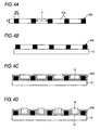
- FIGs. 4 to 6 are views describing the manufacturing method of the wiring substrate 1A of the first embodiment of the invention.
- a reinforcing body 50A is first prepared as shown in Fig. 4 (A) .
- This reinforcing body 50A has the mesh shape as described above and is formed by metal, glass, silicon, ceramic, etc.
- the reinforcing body 50A used in the embodiment is a reinforcing body previously manufactured in a manufacturing step different from a manufacturing step of a wiring substrate 1A.
- a protective tape 13 is arranged on this reinforcing body 50A.
- This protective tape 13 is, for example, a resin tape to which an adhesive is applied and a thickness of the tape is, for example, 100 ⁇ m.
- Cu foil 14 (a metal film described in the claim) is arranged on a surface of the protective tape 13.
- This Cu foil 14 has, for example, a thickness of 18 ⁇ m and is stuck on an upper surface of the protective tape 13 and a surface of the reinforcing body 50A using a vacuum laminate method.
- a resist material 16 is formed on a formation position of a first wiring layer 18 described below of the Cu foil 14.
- the resist material 16 is formed by first arranging a dry film on the upper surface of the protective tape 13 and patterning this dry film.
- it may be constructed so that an opening part is previously formed excluding the formation position of the first wiring layer 18 with respect to a dry filmy resist film and this is arranged on the protective tape 13.
- etching processing is performed with respect to the Cu foil 14 using the resist material 16 as a mask.
- the resist material 16 is removed and thereby the first wiring layer 18 is formed as shown in Fig. 5(B) .
- an insulating layer half body 20-1 is formed on the protective tape 13 so as to cover the first wiring layer 18 and the reinforcing body 50A as shown in Fig. 5(C) .
- this insulating layer half body 20-1 As a material of this insulating layer half body 20-1, a resin material such as an epoxy resin or a polyimide resin is used. Also, as one example of a formation method of the insulating layer half body 20-1, the insulating layer half body 20-1 can be obtained by thermally treating a resin film at temperatures of 130 to 150 °C and curing the resin film while pressing (pressing) the resin film after the resin film is laminated to the protective tape 13.
- the protective tape 13 is peeled from the insulating layer half body 20-1 as shown in Fig. 5 (D) .
- the first wiring layer 18 and the reinforcing body 50A are configured to be buried inside the insulating layer half body 20-1, so that the first wiring layer 18 and the reinforcing body 50A are not peeled together with this protective tape 13 even when the protective tape 13 is peeled.
- an insulating layer half body 20-2 is arranged on a lower surface of the insulating layer half body 20-1.
- a resin material such as an epoxy resin or a polyimide resin can be used in a manner similar to the insulating layer half body 20-1.
- the insulating layer half body 20-2 can be formed by the same formation method as that of the insulating layer half body 20-1 and concretely, the insulating layer half body 20-2 can be obtained by thermally treating a resin film at temperatures of 130 to 150 °C and curing the resin film while pressing (pressing) the resin film after the resin film is laminated to the insulating layer half body 20-1. Consequently, a first insulating layer 20 made of the insulating layer half body 20-1 and the insulating layer half body 20-2 is formed.
- first via holes 20W are formed in the first insulating layer 20 so as to expose a connection pad 18 using a laser processing method etc. Formation of the first via holes 20W by this laser processing is implemented with respect to both of the insulating layer half body 20-1 and the insulating layer half body 20-2. As a result of this, the first wiring layer 18 is in a state of being exposed from the first insulating layer 20 in both of the upper and lower surfaces as shown in Fig. 6(A) .
- a second wiring layer 18a is formed with respect to the first insulating layer 20 using a semi-additive method.
- electroless Cu plating is performed on an upper surface of the first insulating layer 20 and inner surfaces of the first via holes 20W and thereby, a seed layer is formed.
- patterning is performed so as to leave the portion other than a formation position of the first wiring layer 18a while arranging a resist material.
- the second wiring layer 18a is formed by performing electrolytic plating of Cu using the seed layer as a power feeding layer.
- the resist material and the seed layer are removed and thereby a base body 17 shown in Fig. 6 (B) is formed.
- the base body 17 formed in this manner has a structure of bonding a base half body 17a in which the reinforcing body 50A, the first wiring layer 18 and the second wiring layer 18a are formed inside the insulating layer half body 20-1 to a base half body 17b in which the second wiring layer 18a is formed in the insulating layer half body 20-2.
- second insulating layers 20a and third wiring layers 18b are formed on upper and lower surfaces of this base body 17.
- the second insulating layers 20a and the third wiring layers 18b are formed using a build-up method and a semi-additive method.
- the second insulating layers 20a are formed on both surfaces of the base body 17 and second via holes 20X are formed in formation positions of vias with respect to the second insulating layers 20a by laser processing.
- electroless Cu plating is performed on a surface of the second insulating layer 20a and inner surfaces of the second via holes 20X and thereby, a seed layer is formed.
- patterning is performed so as to leave the portion other than a formation position of the third wiring layer 18b while arranging a resist material.
- the third wiring layer 18b is formed by performing electrolytic plating of Cu using the seed layer as a power feeding layer.
- the resist material and the seed layer are removed and thereby a wiring member 30A shown in Fig. 6 (C) is formed.
- the wiring substrate 1A shown in Fig. 2 is manufactured by forming a solder resist 22 and pad surface plated layers 25, 26.
- the build-up wiring layer with a total of four layers is formed, but a build-up wiring layer with n layers (n is an integer of one or more) may be formed.
- each of the insulating layers 20, 20a and each of the wiring layers 18, 18a, 18b are formed around an arrangement position of the reinforcing body 50A, so that vertical balance around the reinforcing body 50A improves and occurrence of internal stress can be suppressed. Also, the reinforcing body 50A is constructed by only one layer of the center, so that a member cost can be reduced.
- Fig. 7 is a sectional view showing a wiring substrate 1B which is the second embodiment
- Figs. 8 to 10 show a manufacturing method of the wiring substrate 1B.
- the description shall properly be omitted by assigning the same numerals to configurations corresponding to the configurations shown in Figs. 2 to 6 used in the description of the first embodiment.
- the wiring substrate 1A according to the first embodiment described above is configured to form each of the insulating layers 20, 20a and each of the wiring layers 18, 18a, 18b around an arrangement position of the reinforcing body 50A, shapes of via parts formed in each of the wiring layers 18, 18a, 18b are also formed in the shapes layered symmetrically around the arrangement position of the reinforcing body 50A.
- the wiring substrate 1B according to the present embodiment is characterized in that each of the insulating layers 20, 20a, 20b, 20c and wiring layers 18, 18a, 18b, 18c, 18d are sequentially layered and formed from the first insulating layer 20 toward the fourth insulating layer 20c. As a result of this, a shape of a via part formed in each of the wiring layers 18a, 18b, 18c, 18d is formed in the same direction.
- a reinforcing body 50A is arranged in a center position of a wiring member 30B in a manner similar to the wiring substrate 1A according to the first embodiment, so that the wiring member 30B can surely be reinforced and even when stress or external force is applied from various directions, the wiring substrate 1B can effectively be prevented from being deformed and also weight reduction in the wiring substrate 1B can be achieved. Also, wiring members with the same configuration can be formed on both surfaces of a support body 10, so that productivity can be improved.
- a support body 10 is first prepared as shown in Fig. 8 (A) .
- copper foil is used as the support body 10.
- a thickness of this copper foil is, for example, 35 to 100 ⁇ m.
- a solder resist 21 and a pad surface plated layer 25 are formed on this support body 10.
- an opening part is formed in a predetermined position and the pad surface plated layer 25 is formed inside this opening part.
- This pad surface plated layer 25 has a structure of layering an Au film, a Pd film and an Ni film, and can be formed using, for example, a plating method or a sputtering method.
- a resist film (not shown) is formed on this support body 10 and also patterning processing is performed with respect to this resist film and an opening part is formed in a position corresponding to a formation position of a connection pad 18.
- a first wiring layer 18 is formed on the support body 10 by electrolytic plating of Cu using the support body 10 in a plated power feeding layer. In this case, the first wiring layer 18 is also formed on the pad surface plated layer 25. Subsequently, by removing the resist film, the first wiring layer 18 with a predetermined shape is formed on the support body 10 as shown in Fig. 8(B) .
- this connection pad 18 functions as an external connection terminal of the wiring substrate 1B.
- a first insulating layer 20 for covering the connection pad 18 is formed in the support body 10.
- a resin material such as an epoxy resin or a polyimide resin is used.
- the first insulating layer 20 can be obtained by thermally treating a resin film at temperatures of 130 to 150 °C and curing the resin film while pressing (pressing) the resin film after the resin film is laminated to the support body 10.
- a first via hole 20W is formed in the first insulating layer 20 formed in the support body 10 so as to expose the connection pad 18 using a laser processing method etc.
- a second wiring layer 18a connected to the connection pad 18 formed on the support body 10 through the first via hole 20W is formed.
- This second wiring layer 18a is made of copper (Cu) and is formed on the first insulating layer 20.
- This second wiring layer 18a is formed by, for example, a semi-additive method.
- a resist film including an opening part corresponding to the second wiring layer 18a is formed after a Cu seed layer is formed on an upper surface of the first insulating layer 20 and the first via hole 20W by electroless plating or a sputtering method.
- a Cu layer pattern is formed in an opening part of the resist film by electrolytic plating using the Cu seed layer in a plated power feeding layer.
- the second wiring layer 18a is obtained by etching the Cu seed layer using the Cu layer pattern as a mask after the resist film is removed.
- various wiring formation methods such as a subtractive method in addition to the semi-additive method described above can be adopted as a formation method of the second wiring layer 18a.
- a second via hole 20X is formed in the portion of a second insulating layer 20a on the second wiring layer 18a after the second insulating layer 20a for covering the second wiring layer 18a is formed in the support body 10 by repeating steps similar to the above. Further, a third wiring layer 18b connected to the second wiring layer 18a through the second via hole 20X is formed on the second insulating layer 20a of the support body 10.
- Fig. 9(A) shows the support body 10 in which the third wiring layer 18b is formed.
- a state of forming this third wiring layer 18b is a state of forming a wiring member 30B to about half the thickness with respect to a thickness direction of the wiring member 30B.
- a reinforcing body 50A is subsequently installed on an upper surface of the second insulating layer 20a.
- the reinforcing body 50A is a reinforcing body previously manufactured in a manufacturing step different from a manufacturing step of the wiring substrate 1B.
- This reinforcing body 50A is temporarily joined to an upper part of the second insulating layer 20a using an adhesive.
- the reinforcing body 50A it is necessary to place the reinforcing body 50A on the second insulating layer 20a so as not to interfere with the third wiring layer 18b. As a result of this, it may be constructed so that a guide pin (not shown) for positioning is previously disposed and thereby the reinforcing body 50A is placed on the second insulating layer 20a with high accuracy.
- a third insulating layer 20b is formed in the support body 10 so as to cover the reinforcing body 50A and the third wiring layer 18b as shown in Fig. 9(C) .
- a third via hole 20Y communicating with the third wiring layer 18b is formed in a predetermined portion of the third insulating layer 20b on the third wiring layer 18b by laser processing.
- a fourth wiring layer 18c connected to the third wiring layer 18b through the third via hole 20Y is formed on the third insulating layer 20b.
- a fourth insulating layer 20c is formed so as to cover this fourth wiring layer 18c.
- a fourth via hole 20Z communicating with the fourth wiring layer 18c is formed in a predetermined portion of the fourth insulating layer 20c on the fourth wiring layer 18c by laser processing.
- a fifth wiring layer 18d connected to the fourth wiring layer 18c through the fourth via hole 20Z is formed on the fourth insulating layer 20c.
- the wiring member 30B is formed by passing through the steps described above.
- the build-up wiring layer with five layers (first to fifth wiring layers 18 to 18d) is formed, but a build-up wiring layer with n layers (n is an integer of one or more) may be formed.
- a solder resist 22 in which an opening part is disposed in a predetermined position is formed on the fourth insulating layer 20c as shown in Fig. 10 (C) .
- the fifth wiring layer 18d exposed to the inside of the opening part of this solder resist 22 results in an external connection terminal.
- a pad surface plated layer 26 is formed on a surface of the fifth wiring layer 18d exposed from this opening part. This pad surface plated layer 26 has the same configuration as that of the pad surface plated layer 25 described above.
- the support body 10 functioning as the support body is removed.
- This support body 10 can be removed by wet etching using a ferric chloride aqueous solution, a cupric chloride aqueous solution or an ammonium persulfate aqueous solution, etc.
- the pad surface plated layer 25 is formed on the uppermost surface, so that the support body 10 can be selectively etched and removed with respect to the first wiring layer 18 and the first insulating layer 20. Consequently, the wiring substrate 1B shown in Fig. 7 is manufactured.
- each of the insulating layers 20, 20a, 20b, 20c and each of the wiring layers 18, 18a, 18b, 18c, 18d are layered on the robust support body 10, so that each of the insulating layers and the wiring layers can be formed with high accuracy and also the reinforcing body 50A can be installed in a proper position. Consequently, interference between the reinforcing body 50A and the third and fourth wiring layers 18b, 18c can be prevented and the wiring substrate 1B can be manufactured with high reliability.
- the manufacturing method and the configuration in which the wiring member 30B is formed on one surface of the support body 10 is shown, but the wiring members 30B in which the reinforcing bodies 50A are disposed can also be formed on both surfaces of the support body 10.
- two wiring substrates 1B can be manufactured using one support body 10, so that manufacturing efficiency can be improved.
- Fig. 11 is a sectional view showing a wiring substrate 1C which is the third embodiment
- Figs. 12 and 13 show a manufacturing method of the wiring substrate 1C.
- the description shall properly be omitted by assigning the same numerals to configurations corresponding to the configurations shown in Figs. 7 to 10 used in the description of the second embodiment.
- the wiring substrate 1B according to the second embodiment described above is configured to use the reinforcing body 50A manufactured in a step different from the manufacturing step of the wiring substrate 1B.
- the present embodiment is characterized in that a reinforcing body 50B is simultaneously formed inside a manufacturing step of the wiring substrate 1C. Because of this, in the wiring substrate 1C according to the embodiment, the reinforcing body 50B is formed by Cu which is the same material as that of a wiring layer.
- this reinforcing body 50B is formed by the same material as that of the wiring layer thus, this reinforcing body 50B is configured to cross plural linear members and thereby, a wiring member 30C can surely be reinforced and even when stress or external force is applied from various directions, the wiring substrate 1C can effectively be prevented from being deformed and further weight reduction in the wiring substrate 1C can be achieved. Also, by preventing the occurrence of deformation as described above, handling of the wiring substrate 1C is facilitated and thus, the occurrence of breakage or a crack at the time of handling can be prevented.
- a seed layer 27 made of Cu is formed on an upper surface of a second insulating layer 20a and an upper surface of a third wiring layer 18b when the third wiring layer 18b is formed in the second insulating layer 20a as shown in Fig. 12(A) .
- a resist material is formed in an upper part on which the seed layer 27 is formed and also, patterning for removing the portion excluding a formation position of a reinforcing body 50B is performed.
- Fig. 12 (B) shows a resist material 28 in which the patterning is performed. This resist material 28 is formed so as to cover the third wiring layer 18b.
- the reinforcing body 50B is formed between each of the resist materials 28.
- Cu is used as a material of the reinforcing body 50B, so that the electrolytic plating of Cu is performed, but when another material (for example, Ni) is used as the material of the reinforcing body 50B, electrolytic plating by the material (Ni) is performed.
- Fig. 13(B) shows a state of removing the resist material 28.
- Fig. 13 (C) corresponds to Fig. 10 (B)
- Fig. 13 (D) corresponds to Fig. 10(C) .
- the reinforcing body 50B can be formed collectively in a step of building up each of the insulating layers 20, 20a, 20b, 20c and each of the wiring layers 18, 18a, 18b, 18c, 18d, so that the wiring substrate 1C having the reinforcing body 50B can be manufactured easily at low cost. Also, a shape of the reinforcing body 50B can be changed relatively easily by properly changing the patterning of the resist material 28. Also, unlike the other embodiments described above, a step of mounting the reinforcing body is absent, so that the reinforcing body 50B can be formed by appropriating the existing process apparatus of build-up.
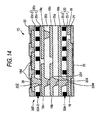
- Fig. 14 is a sectional view showing a wiring substrate 1D which is the fourth embodiment, and Figs. 15 to 17 show a manufacturing method of the wiring substrate 1D.
- the wiring substrates 1B, 1C according to the second and third embodiments described above are configured to form the reinforcing bodies 50A, 50B in the center positions of the wiring members 30B, 30C. As a result of this, in the manufacturing steps of the wiring substrates 1B, 1C, the step of arranging the reinforcing bodies 50A, 50B is performed only one time.
- the wiring substrate 1D according to the present embodiment is characterized by having a configuration in which a reinforcing body 50A-1 and a reinforcing body 50A-2 are arranged with space upward and downward across a center position with respect to a thickness direction of a wiring member 30D. Therefore, in a manufacturing step of the wiring substrate 1D, processing for installing the reinforcing body is performed plural times (two times in the embodiment).
- the plural reinforcing body 50A-1 and reinforcing body 50A-2 are present inside the wiring member 30D, so that deformation of the wiring substrate 1D resulting from stress or external force can be prevented more surely.
- a support body 10 is first prepared as shown in Fig. 15(A) .
- copper foil is used as the support body 10.
- a solder resist 21 and a pad surface plated layer 25 are formed on the support body 10 in a manner similar to that described in the second embodiment.
- a first wiring layer 18 is formed on this support body 10 by a method similar to that described in the second and third embodiments. Subsequently, an insulating layer half body 20-1 is formed in an upper part of the support body 10 on which this first wiring layer 18 is formed.
- This insulating layer half body 20-1 has the same material as the material of the insulating layer used in each of the embodiments described above, and a resin material such as an epoxy resin or a polyimide resin is used.
- a first reinforcing body 50A-1 is installed on an upper part of this insulating layer half body 20-1 as shown in Fig. 15 (B) .
- This first reinforcing body 50A-1 has the same configuration as that of the reinforcing body 50A used in the first and second embodiments described above.
- This reinforcing body 50A-1 is temporarily joined on the insulating layer half body 20-1 using an adhesive. Also, it may be configured to be positioned using a guide pin as described above in the case of this temporary joint.
- an insulating layer half body 20-2 is subsequently formed on the insulating layer half body 20-1 so as to cover the reinforcing body 50A-1.
- This insulating layer half body 20-2 also has a resin material such as an epoxy resin or a polyimide resin, and can be formed by thermally treating a resin film at temperatures of 130 to 150 °C and curing the resin film while pressing (pressing) the resin film after the resin film made of the resin material is laminated to the insulating layer half body 20-1.
- the insulating layer half body 20-1 is integrated with the insulating layer half body 20-2 and hence, a first insulating layer 20 is formed as shown in Fig. 15(C) .
- a first via hole 20W is formed in the first insulating layer 20 so as to expose a connection pad 18 using a laser processing method etc.
- a second wiring layer 18a connected to the connection pad 18 formed on the support body 10 through the first via hole 20W is formed using the semi-additive method described above.
- Fig. 16(A) shows a state of forming the second wiring layer 18a.
- a second insulating layer 20a, a third wiring layer 18b, a third insulating layer 20b and a fourth wiring layer 18c are formed on an upper part of the second wiring layer 18a.
- Fig. 16(B) shows a state of layering and forming each of the insulating layers 20, 20a, 20b and each of the wiring layers 18, 18a, 18b, 18c.
- an insulating layer half body 20c-1 is formed in an upper part of the third insulating layer 20b on which this fourth wiring layer 18c is formed.
- This insulating layer half body 20c-1 also has the same material as the material of the insulating layer used in each of the embodiments described above, and a resin material such as an epoxy resin or a polyimide resin is used. Also, it is desirable to set a thickness of this insulating layer half body 20c-1 at about 10 ⁇ m in a manner similar to the insulating layer half body 20-1.
- a second reinforcing body 50A-2 is installed on an upper part of this insulating layer half body 20c-1 as shown in Fig. 16 (C) .
- This second reinforcing body 50A-2 also has the same configuration as that of the reinforcing body 50A used in the first and second embodiments described above.
- This reinforcing body 50A-2 is temporarily joined on the insulating layer half body 20c-1 using an adhesive. Also, it may be configured to be positioned using a guide pin as described above in the case of this temporary joint.
- an insulating layer half body 20c-2 is subsequently formed on the insulating layer half body 20c-1 so as to cover the reinforcing body 50A-2.
- This insulating layer half body 20c-2 also has a resin material such as an epoxy resin or a polyimide resin, and is formed in a manner similar to that of the insulating layer half body 20-2. Consequently, the insulating layer half body 20c-1 is integrated with the insulating layer half body 20c-2 and hence, a fourth insulating layer 20c is formed as shown in Fig. 16(D) .
- a fourth via hole 20Z is formed in the fourth insulating layer 20c so as to expose the fourth wiring layer 18c using a laser processing method etc.
- a fifth wiring layer 18d connected to the fourth wiring layer 18c through the fourth via hole 20Z is formed using the semi-additive method described above.
- Fig. 17(B) shows a state of forming the fifth wiring layer 18d.
- the wiring member 30D is formed by passing through the steps described above.
- the build-up wiring layer with five layers (first to fifth wiring layers 18 to 18d) is formed, but a build-up wiring layer with n layers (n is an integer of one or more) may be formed.
- a solder resist 22 in which an opening part is disposed in a predetermined position is formed on the fourth insulating layer 20c as shown in Fig. 17 (C) .
- the fifth wiring layer 18d exposed to the inside of the opening part of this solder resist 22 results in an external connection terminal.
- a pad surface plated layer 26 is formed on a surface of the fifth wiring layer 18d exposed from this opening part. This pad surface plated layer 26 has the same configuration as that of the pad surface plated layer 25 described above.
- the support body 10 functioning as the support body is removed in a manner similar to the second and third embodiments described above. Consequently, the wiring substrate 1D shown in Fig. 14 is manufactured.
- the plural reinforcing bodies 50A-1, 50A-2 can easily be incorporated into the wiring member 30D and the wiring substrate 1D capable of effectively preventing occurrence of deformation can easily be manufactured.
- the shapes of the reinforcing bodies 50A, 50A-1, 50A-2, 50B are formed in the mesh shape as shown in Fig. 3 , but are not limited to this mesh shape.
- it may be configured to be placed so as to cross linear members 51B in a cross shape in plan view as described in a wiring substrate 1E shown in Fig. 18(A) .
- a reinforcing body 50D placed so as to cross two reinforcing bodies 51B in a diagonal shape of a wiring substrate 1F in plan view may be used as described in the wiring substrate 1F shown in Fig. 18(B) .
- a reinforcing body 50E configured so as to cross plural linear members 51B in an asterisk shape may be used as described in a wiring substrate 1G shown in Fig. 18(C) .
- a form of crossing of the linear members constructing the reinforcing body can properly be changed according to a direction or a size of stress occurring inside the wiring substrate or an application direction or a size of external force which expects to be applied to the wiring substrate.
- numeral 11 shows an outline of a semiconductor chip mounted in each of the wiring substrates 1E to 1G.
- the shapes of the linear members 51A, 51B constructing the reinforcing bodies 50A to 50E, 50-1, 50-2 are formed in the straight line shape, but it may be configured to form linear members 51A, 51B in a curved line shape, a serration shape or other shapes and cross the linear members.
- the surface (the surface in which the first wiring layer 18 is formed) in which the support body 10 is removed is used as the surface to which the external connection terminal is connected and the opposite surface (the surface of the side in which the fifth wiring layer 18d is formed) is used as the chip installation surface.
- the surface in which the support body 10 is removed can be used as the chip installation surface and the opposite surface can also be used as the surface to which the external connection terminal is connected.
- the wiring members 30B in which the reinforcing bodies 50A are disposed can also be formed on both surfaces of the support body 10 and in the case of using this configuration, two wiring substrates 1B can be manufactured using one support body 10, so that manufacturing efficiency can be improved. This similarly applies to each of the embodiments subsequent to the third embodiment.
- a layered body layered by bonding two support bodies is fabricated and wiring substrates (wiring members) are formed on both surfaces of this layered body by the method described in each of the embodiments and thereafter the bond part is removed and thereby the layered body is separated into each of the support bodies and then each of the support bodies is removed and thereby the wiring substrates are formed.
- wiring substrates wiring members
Landscapes
- Engineering & Computer Science (AREA)
- Microelectronics & Electronic Packaging (AREA)
- Manufacturing & Machinery (AREA)
- Structure Of Printed Boards (AREA)
- Production Of Multi-Layered Print Wiring Board (AREA)
Abstract
Description
- The present invention relates to a wiring substrate and a manufacturing method thereof. In particular it relates to a wiring substrate made by disposing a reinforcing member in a wiring member formed by removing a support body after a wiring layer and an insulating layer are layered on the support body and a manufacturing method of the wiring substrate.
- For example, a method for manufacturing a wiring substrate in which an electronic component is mounted includes a method for obtaining a wiring substrate by separating a wiring layer from a support body after a necessary wiring layer is formed in a state capable of being peeled on the support body. In the manufacturing method of the wiring substrate of this kind, there is the support body at the time of forming a build-up wiring layer, so that the build-up wiring layer can surely be formed with high accuracy. Also, after the build-up wiring layer is formed, the support body is removed, so that improvement in electrical characteristics and thinning of the wiring substrate manufactured can be achieved.
-
Fig. 1(A) shows one example of a wiring substrate manufactured by this manufacturing method. Awiring substrate 100 shown inFig. 1(A) is constructed so that awiring member 101 is formed by layeringwiring layers 102 andinsulating layers 103 andupper electrode pads 107 are formed on an upper part of the wiring member and alsolower electrode pads 108 are formed on a lower part of the wiring member. Also, it is constructed so thatsolder bumps 110 are formed on theupper electrode pads 107 and also thelower electrode pads 108 are exposed from asolder resist 109 formed on a lower surface of thewiring member 101. - However, the
wiring substrate 100 in which a support body is completely removed has a small mechanical strength of the substrate itself. Hence, there is a problem of easily deforming thewiring substrate 100 when external force is applied as shown inFig. 1(B) . - As a result of this, means in which a reinforcing
member 106 is arranged by adhesion etc. so as to surround a formation region of theupper electrode pads 107 on thewiring member 101 and thereby a mechanical strength of thewiring substrate 100 is improved has been proposed as disclosed in Patent Reference 1 (the reinforcingmember 106 is shown by a chain line inFig. 1(A) ). - [Patent Reference 1]
JP-A-2000-323613 - In the configuration fixed so as to stack the reinforcing
member 106 on a surface of thewiring member 101 as described above, a thickness as a whole of thewiring substrate 100 increases and it cannot respond to the needs of thinning. Also, there is the reinforcingmember 106 made of a metal material with a large shape on a surface of thewiring substrate 100, so that there is also a problem that the reinforcingmember 106 may hinder mounting depending on a form of a semiconductor element mounted in thewiring substrate 100. - The invention has been implemented in view of the problems described above, and an object of the invention is to provide a wiring substrate capable of improving a mechanical strength while achieving thinning, and a manufacturing method of the wiring substrate.
In light of the above, the wiring substrate according toindependent claim 1, the manufacturing method according toindependent claim 5, and the manufacturing method of claim 6 are provided.
Further advantages, features, aspects and details are evident from the dependent claims, the description and the drawings. - According to a first aspect of the invention, there is provided a wiring substrate including:
- a wiring member made by layering an insulating layer and a wiring layer, and
- a reinforcing body disposed between the insulating layers of the wiring member, wherein
- the reinforcing body is configured to cross plural linear members.
- According to a second aspect of the invention, there is provided the wiring substrate as in the first aspect, wherein
the reinforcing body is arranged in a center position with respect to a thickness direction of the wiring member. - According to a third aspect of the invention, there is provided the wiring substrate as in the first aspect, wherein
the reinforcing bodies are arranged with space upward and downward across a center position with respect to a thickness direction of the wiring member. - According to a forth aspect of the invention, there is provided the wiring substrate as in any one of the first to third aspects, wherein
the reinforcing body has a shape selected from at least a cross shape, an asterisk shape and a mesh shape in plan view. - According to a fifth aspect of the invention, there is provided a manufacturing method of a wiring substrate, including the steps of:
arranging a protective member in a reinforcing body configured to cross plural linear members, - forming an electrode on the protective member by a metal film,
- forming a base half body by forming a first resin member to cover the reinforcing body and the protective member,
- removing the protective member from the base half body and arranging a second resin material on a surface in which the protective member is removed,
- forming an opening part for exposing the electrode in the first and second resin members,
- forming a base body by forming a wiring metal layer on the inside of the opening part and surfaces of the first and second resin members, and
- layering a wiring layer and an insulating layer on the base body to form a wiring member.
- According to a sixth aspect of the invention, there is provided a manufacturing method of a wiring substrate, including the steps of:
- layering a wiring layer and an insulating layer on a support body to form a wiring member,
- removing the support body from the wiring member, and
- disposing a reinforcing body configured to cross plural linear members on the insulating layer during formation of the wiring member, namely, after at least the wiring layer or the insulating layer is formed on the support body.
- According to a seventh aspect of the invention, there is provided the manufacturing method of a wiring substrate as in the sixth aspect, wherein
the step of disposing the reinforcing body is performed plural times during formation of the wiring member, namely, after at least the wiring layer or the insulating layer is formed on the support body. - According to an eighth aspect of the invention, there is provided the manufacturing method of a wiring substrate as in the sixth aspect, wherein
the step of disposing the reinforcing body is performed one time in a case of forming the wiring member to half of the predetermined thickness during formation of the wiring member, namely, after at least the wiring layer or the insulating layer is formed on the support body. - According to a ninth aspect of the invention, there is provided the manufacturing method of a wiring substrate as in any one of the sixth to eighth aspects, wherein
the reinforcing body is provided on the insulating layer in the step of disposing the reinforcing body.
According to a tenth aspect of the invention, there is provided the manufacturing method of a wiring substrate as in any one of the sixth to eighth aspects, wherein
the step of disposing the reinforcing body includes processing for forming the reinforcing body on the insulating layer using a plating method. - According to the invention, by disposing a reinforcing body configured to cross plural linear members between the insulating layers of a wiring member, even when stress or external force is applied to a wiring substrate from various directions, the plural linear members subjected to the stress etc. are configured to be crossed, so that the stress etc. from all directions can be reduced. Also, weight reduction in the wiring substrate can be achieved as compared with a conventional flat plate-shaped reinforcing body.
An embodiment of the invention may be directed to a wiring substrate having a wiring member made by layering insulating layers and wiring layers, and a reinforcing body disposed between the insulating layers of this wiring member, this reinforcing body is configured to cross plural linear members.
Embodiments are also directed to apparatuses for carrying out the disclosed methods and including apparatus parts for performing described method steps. Furthermore, embodiments are also directed to methods by which the described apparatus operates or by which the described apparatus is manufactured. It may include method steps for carrying out functions of the apparatus or manufacturing parts of the apparatus. The method steps may be performed by way of hardware components, firmware, software, a computer programmed by appropriate software, by any combination thereof or in any other manner. - So that the manner in which the above recited features of the present invention can be understood in detail, a more particular description of the invention, briefly summarized above, may be had by reference to embodiments. The accompanying drawings relate to embodiments of the invention and are described in the following:
-
Figs. 1(A) and 1(B) are diagrams describing a wiring substrate which is one conventional example and its problem. -
Fig. 2 is a partially sectional view of a wiring substrate of a first embodiment of the invention. -
Fig. 3 is a plan view of the wiring substrate of the first embodiment of the invention. -
Figs. 4(A) to 4(D) are sectional views describing a manufacturing method of the wiring substrate of the first embodiment of the invention (first). -
Figs. 5(A) to 5(E) are sectional views describing a manufacturing method of the wiring substrate of the first embodiment of the invention (second). -
Figs. 6(A) to 6(C) are sectional views describing a manufacturing method of the wiring substrate of the first embodiment of the invention (third). -
Fig. 7 is a partially sectional view of a wiring substrate of a second embodiment of the invention. -
Figs. 8(A) to 8(C) are sectional views describing a manufacturing method of the wiring substrate of the second embodiment of the invention (first). -
Figs. 9(A) to 9(D) are sectional views describing a manufacturing method of the wiring substrate of the second embodiment of the invention (second). -
Figs. 10(A) to 10(C) are sectional views describing a manufacturing method of the wiring substrate of the second embodiment of the invention (third). -
Fig. 11 is a partially sectional view of a wiring substrate of a third embodiment of the invention. -
Figs. 12(A) and 12(B) are sectional views describing a manufacturing method of the wiring substrate of the third embodiment of the invention (first). -
Figs. 13(A) to 13(D) are sectional views describing a manufacturing method of the wiring substrate of the third embodiment of the invention (second). -
Fig. 14 is a partially sectional view of a wiring substrate of a fourth embodiment of the invention. -
Figs. 15(A) to 15(D) are sectional views describing a manufacturing method of the wiring substrate of the fourth embodiment of the invention (first). -
Figs. 16(A) to 16(D) are sectional views describing a manufacturing method of the wiring substrate of the fourth embodiment of the invention (second). -
Figs. 17(A) to 17(C) are sectional views describing a manufacturing method of the wiring substrate of the fourth embodiment of the invention (third). -
Figs. 18 (A) to 18 (C) are plan views of a wiring substrate using a reinforcing body which is a modified example of a reinforcing body used in the first embodiment. - Next, the best mode for carrying out the invention will be described together with the drawings.
-
Figs. 2 and3 show awiring substrate 1A which is a first embodiment of the invention.Fig. 2 is a partially sectional view of thewiring substrate 1A, andFig. 3 shows a state of viewing thewiring substrate 1A from the plane. - The
wiring substrate 1A according to the present embodiment is broadly constructed of awiring member 30A and a reinforcingbody 50A. Thiswiring substrate 1A has a rectangular shape in which, for example, a length L1 (shown by an arrow inFig. 3 ) of one side is 30 mm to 50 mm in plan view. For example, a semiconductor chip 11 (only the outline is shown inFig. 3 ) is mounted in thiswiring substrate 1A.
Thewiring member 30A is constructed of abase body 17, asecond wiring layer 18a, athird wiring layer 18b and solder resists 21, 22, etc. Thebase body 17 is disposed in substantially the center position of thewiring member 30A. Thisbase body 17 is constructed of a basehalf body 17a located upward and a basehalf body 17b located downward. - The base
half body 17a is constructed of an insulating layer half body 20-1 formed by a resin material such as an epoxy resin or a polyimide resin, thesecond wiring layer 18a and afirst wiring layer 18 formed in this insulating layer half body 20-1. Thefirst wiring layer 18 is formed in a position of bonding between the basehalf body 17a and the basehalf body 17b. Also, thesecond wiring layer 18a is constructed of a wiring part and a via part, and the via part is configured to be connected to thefirst wiring layer 18. - On the other hand, the base
half body 17b is constructed of an insulating layer half body 20-2 formed by a resin material such as an epoxy resin or a polyimide resin and thesecond wiring layer 18a formed in this insulating layer half body 20-2. Thissecond wiring layer 18a is constructed of a wiring part and a via part, and the via part is configured to be connected to thefirst wiring layer 18. Therefore, thesecond wiring layer 18a formed in the basehalf body 17a is configured to be electrically connected to thesecond wiring layer 18a formed in the basehalf body 17b through thefirst wiring layer 18. - A second insulating
layer 20a, thethird wiring layer 18b and the solder resists 21, 22, etc. are configured to be arranged in an upper part and a lower part of thebase body 17 configured above. The secondinsulating layer 20a is formed by a resin material such as an epoxy resin or a polyimide resin and also, thethird wiring layer 18b is formed by Cu (copper). This secondinsulating layer 20a and thethird wiring layer 18b are respectively formed on both of upper and lower surfaces of thebase body 17 using a build-up method as described below. - The solder resists 21, 22 cover the front of the
wiring member 30A excluding the portion used as an external connection terminal of thethird wiring layer 18b. Also, pad surface platedlayers third wiring layer 18b. The pad surface platedlayers - The reinforcing
body 50A is arranged in substantially the center position with respect to a thickness direction of thewiring member 30A. Concretely, the reinforcingbody 50A is arranged in a state of being sandwiched between a pair of the insulating layer half bodies 20-1, 20-2 in a position of the boundary between the basehalf body 17a and the basehalf body 17b of the inside of thebase body 17. This reinforcingbody 50A is configured to cross plurallinear members 51A with straight line shapes and have a mesh shape as a whole as shown inFig. 3 . - Metal, glass, silicon, ceramic, hard resin or a copper clad layered plate, etc. can be applied to each of the
linear members 51A. Also, a width W1 and a height H (seeFig. 4 for the height H) of each of thelinear members 51A can be selected in the range of 50 µm to 400 µm, and are preferably set at 100 µm in its range. Also, a pitch P between the adjacentlinear members 51A can be selected in the range of 200 µm to 800 µm, and is preferably set at 500 µm in its range. In addition, inFig. 3 , the reinforcingbody 50A is shown as a uniform mesh structure, but a mesh shape is properly deformed so as not to interfere with the first and second wiring layers 18, 18a. - According to the
wiring substrate 1A according to the embodiment as described above, even when internal stress by application of heat occurs inside thewiring substrate 1A and also external force is applied to thewiring substrate 1A, the reinforcingbody 50A is subjected to this stress or external force, and these forces are not applied to the insulatinglayers - Further, the reinforcing
body 50A according to the embodiment has a beam structure in which the plurallinear members 51A are crossed unlike a mesh into which fibers are woven. As a result of this, it can cope also with external force and stress from various directions and thus, thewiring substrate 1A can effectively be prevented from being deformed. - Also, the reinforcing
body 50A according to the embodiment has a mesh shape in which multiple space parts are present in the inside, so that weight reduction in the wiring substrate can also be achieved as compared with a conventional frame-shaped reinforcing body. - Next, a manufacturing method of the
wiring substrate 1A mentioned above will be described.Figs. 4 to 6 are views describing the manufacturing method of thewiring substrate 1A of the first embodiment of the invention. - In the case of manufacturing the
wiring substrate 1A, a reinforcingbody 50A is first prepared as shown inFig. 4 (A) . This reinforcingbody 50A has the mesh shape as described above and is formed by metal, glass, silicon, ceramic, etc. In addition, the reinforcingbody 50A used in the embodiment is a reinforcing body previously manufactured in a manufacturing step different from a manufacturing step of awiring substrate 1A. - As shown in
Fig. 4(B) , aprotective tape 13 is arranged on this reinforcingbody 50A. Thisprotective tape 13 is, for example, a resin tape to which an adhesive is applied and a thickness of the tape is, for example, 100 µm. - Next, as shown in
Fig. 4(C) , Cu foil 14 (a metal film described in the claim) is arranged on a surface of theprotective tape 13. ThisCu foil 14 has, for example, a thickness of 18 µm and is stuck on an upper surface of theprotective tape 13 and a surface of the reinforcingbody 50A using a vacuum laminate method. - Then, as shown in
Fig. 4(D) , a resistmaterial 16 is formed on a formation position of afirst wiring layer 18 described below of theCu foil 14. In the case of forming this resistmaterial 16, the resistmaterial 16 is formed by first arranging a dry film on the upper surface of theprotective tape 13 and patterning this dry film. In addition, it may be constructed so that an opening part is previously formed excluding the formation position of thefirst wiring layer 18 with respect to a dry filmy resist film and this is arranged on theprotective tape 13. - Then, as shown in
Fig. 5(A) , etching processing is performed with respect to theCu foil 14 using the resistmaterial 16 as a mask. When this etching processing is ended, the resistmaterial 16 is removed and thereby thefirst wiring layer 18 is formed as shown inFig. 5(B) . - When the
first wiring layer 18 is formed on theprotective tape 13 thus, an insulating layer half body 20-1 is formed on theprotective tape 13 so as to cover thefirst wiring layer 18 and the reinforcingbody 50A as shown inFig. 5(C) . - As a material of this insulating layer half body 20-1, a resin material such as an epoxy resin or a polyimide resin is used. Also, as one example of a formation method of the insulating layer half body 20-1, the insulating layer half body 20-1 can be obtained by thermally treating a resin film at temperatures of 130 to 150 °C and curing the resin film while pressing (pressing) the resin film after the resin film is laminated to the
protective tape 13. - When the insulating layer half body 20-1 is formed as described above, the
protective tape 13 is peeled from the insulating layer half body 20-1 as shown inFig. 5 (D) . In this case, thefirst wiring layer 18 and the reinforcingbody 50A are configured to be buried inside the insulating layer half body 20-1, so that thefirst wiring layer 18 and the reinforcingbody 50A are not peeled together with thisprotective tape 13 even when theprotective tape 13 is peeled. - Subsequently, as shown in
Fig. 5(E) , an insulating layer half body 20-2 is arranged on a lower surface of the insulating layer half body 20-1. As a material of this insulating layer half body 20-2, a resin material such as an epoxy resin or a polyimide resin can be used in a manner similar to the insulating layer half body 20-1. Also, the insulating layer half body 20-2 can be formed by the same formation method as that of the insulating layer half body 20-1 and concretely, the insulating layer half body 20-2 can be obtained by thermally treating a resin film at temperatures of 130 to 150 °C and curing the resin film while pressing (pressing) the resin film after the resin film is laminated to the insulating layer half body 20-1. Consequently, a first insulatinglayer 20 made of the insulating layer half body 20-1 and the insulating layer half body 20-2 is formed. - When the first insulating
layer 20 is formed as described above, first viaholes 20W are formed in the first insulatinglayer 20 so as to expose aconnection pad 18 using a laser processing method etc. Formation of the first viaholes 20W by this laser processing is implemented with respect to both of the insulating layer half body 20-1 and the insulating layer half body 20-2. As a result of this, thefirst wiring layer 18 is in a state of being exposed from the first insulatinglayer 20 in both of the upper and lower surfaces as shown inFig. 6(A) . - Subsequently, formation processing of a
second wiring layer 18a is performed with respect to the first insulatinglayer 20 using a semi-additive method. Concretely, after cleaning by performing desmear processing with respect to the first viaholes 20W, electroless Cu plating is performed on an upper surface of the first insulatinglayer 20 and inner surfaces of the first viaholes 20W and thereby, a seed layer is formed. Subsequently, patterning is performed so as to leave the portion other than a formation position of thefirst wiring layer 18a while arranging a resist material. - Then, the
second wiring layer 18a is formed by performing electrolytic plating of Cu using the seed layer as a power feeding layer. When thesecond wiring layer 18a is formed in this manner, the resist material and the seed layer are removed and thereby abase body 17 shown inFig. 6 (B) is formed. Thebase body 17 formed in this manner has a structure of bonding a basehalf body 17a in which the reinforcingbody 50A, thefirst wiring layer 18 and thesecond wiring layer 18a are formed inside the insulating layer half body 20-1 to a basehalf body 17b in which thesecond wiring layer 18a is formed in the insulating layer half body 20-2. - When the
base body 17 is formed as described above, second insulatinglayers 20a and third wiring layers 18b are formed on upper and lower surfaces of thisbase body 17. The second insulatinglayers 20a and the third wiring layers 18b are formed using a build-up method and a semi-additive method. - Concretely, the second insulating
layers 20a are formed on both surfaces of thebase body 17 and second viaholes 20X are formed in formation positions of vias with respect to the second insulatinglayers 20a by laser processing. Next, after desmear processing is performed with respect to the second viaholes 20X, electroless Cu plating is performed on a surface of the second insulatinglayer 20a and inner surfaces of the second viaholes 20X and thereby, a seed layer is formed. Subsequently, patterning is performed so as to leave the portion other than a formation position of thethird wiring layer 18b while arranging a resist material. - Then, the
third wiring layer 18b is formed by performing electrolytic plating of Cu using the seed layer as a power feeding layer. When thethird wiring layer 18b is formed in this manner, the resist material and the seed layer are removed and thereby awiring member 30A shown inFig. 6 (C) is formed. Subsequently, thewiring substrate 1A shown inFig. 2 is manufactured by forming a solder resist 22 and pad surface platedlayers - According to the manufacturing method described above, each of the insulating
layers body 50A, so that vertical balance around the reinforcingbody 50A improves and occurrence of internal stress can be suppressed. Also, the reinforcingbody 50A is constructed by only one layer of the center, so that a member cost can be reduced. - Next, a second embodiment of the invention will be described.
Fig. 7 is a sectional view showing awiring substrate 1B which is the second embodiment, andFigs. 8 to 10 show a manufacturing method of thewiring substrate 1B. In addition, inFigs. 8 to 10 , the description shall properly be omitted by assigning the same numerals to configurations corresponding to the configurations shown inFigs. 2 to 6 used in the description of the first embodiment. - Since the
wiring substrate 1A according to the first embodiment described above is configured to form each of the insulatinglayers body 50A, shapes of via parts formed in each of the wiring layers 18, 18a, 18b are also formed in the shapes layered symmetrically around the arrangement position of the reinforcingbody 50A. - On the other hand, the
wiring substrate 1B according to the present embodiment is characterized in that each of the insulatinglayers layer 20 toward the fourth insulatinglayer 20c. As a result of this, a shape of a via part formed in each of thewiring layers - However, also in the
wiring substrate 1B according to the embodiment, a reinforcingbody 50A is arranged in a center position of awiring member 30B in a manner similar to thewiring substrate 1A according to the first embodiment, so that thewiring member 30B can surely be reinforced and even when stress or external force is applied from various directions, thewiring substrate 1B can effectively be prevented from being deformed and also weight reduction in thewiring substrate 1B can be achieved. Also, wiring members with the same configuration can be formed on both surfaces of asupport body 10, so that productivity can be improved. - Next, a manufacturing method of the
wiring substrate 1B configured as mentioned above will be described. - In the case of manufacturing the
wiring substrate 1B, asupport body 10 is first prepared as shown inFig. 8 (A) . In the embodiment, copper foil is used as thesupport body 10. A thickness of this copper foil is, for example, 35 to 100 µm. - A solder resist 21 and a pad surface plated
layer 25 are formed on thissupport body 10. In the solder resist 21, an opening part is formed in a predetermined position and the pad surface platedlayer 25 is formed inside this opening part. This pad surface platedlayer 25 has a structure of layering an Au film, a Pd film and an Ni film, and can be formed using, for example, a plating method or a sputtering method. - A resist film (not shown) is formed on this
support body 10 and also patterning processing is performed with respect to this resist film and an opening part is formed in a position corresponding to a formation position of aconnection pad 18. Next, afirst wiring layer 18 is formed on thesupport body 10 by electrolytic plating of Cu using thesupport body 10 in a plated power feeding layer. In this case, thefirst wiring layer 18 is also formed on the pad surface platedlayer 25. Subsequently, by removing the resist film, thefirst wiring layer 18 with a predetermined shape is formed on thesupport body 10 as shown inFig. 8(B) . In addition, thisconnection pad 18 functions as an external connection terminal of thewiring substrate 1B. - Subsequently, a first insulating
layer 20 for covering theconnection pad 18 is formed in thesupport body 10. As a material of this first insulatinglayer 20, a resin material such as an epoxy resin or a polyimide resin is used. As one example of a formation method of the first insulatinglayer 20, the first insulatinglayer 20 can be obtained by thermally treating a resin film at temperatures of 130 to 150 °C and curing the resin film while pressing (pressing) the resin film after the resin film is laminated to thesupport body 10. - Then, a first via
hole 20W is formed in the first insulatinglayer 20 formed in thesupport body 10 so as to expose theconnection pad 18 using a laser processing method etc. Subsequently, asecond wiring layer 18a connected to theconnection pad 18 formed on thesupport body 10 through the first viahole 20W is formed. Thissecond wiring layer 18a is made of copper (Cu) and is formed on the first insulatinglayer 20. Thissecond wiring layer 18a is formed by, for example, a semi-additive method. - Concretely, first, a resist film including an opening part corresponding to the
second wiring layer 18a is formed after a Cu seed layer is formed on an upper surface of the first insulatinglayer 20 and the first viahole 20W by electroless plating or a sputtering method. Next, a Cu layer pattern is formed in an opening part of the resist film by electrolytic plating using the Cu seed layer in a plated power feeding layer. - Subsequently, the
second wiring layer 18a is obtained by etching the Cu seed layer using the Cu layer pattern as a mask after the resist film is removed. In addition, various wiring formation methods such as a subtractive method in addition to the semi-additive method described above can be adopted as a formation method of thesecond wiring layer 18a. - Then, a second via
hole 20X is formed in the portion of a secondinsulating layer 20a on thesecond wiring layer 18a after the second insulatinglayer 20a for covering thesecond wiring layer 18a is formed in thesupport body 10 by repeating steps similar to the above. Further, athird wiring layer 18b connected to thesecond wiring layer 18a through the second viahole 20X is formed on the second insulatinglayer 20a of thesupport body 10.Fig. 9(A) shows thesupport body 10 in which thethird wiring layer 18b is formed. - A state of forming this
third wiring layer 18b is a state of forming awiring member 30B to about half the thickness with respect to a thickness direction of thewiring member 30B. When thewiring member 30B is formed to about half the thickness with respect to its thickness direction thus, a reinforcingbody 50A is subsequently installed on an upper surface of the second insulatinglayer 20a. - In addition, in the embodiment, the reinforcing
body 50A is a reinforcing body previously manufactured in a manufacturing step different from a manufacturing step of thewiring substrate 1B. This reinforcingbody 50A is temporarily joined to an upper part of the second insulatinglayer 20a using an adhesive. - Also, it is necessary to place the reinforcing
body 50A on the second insulatinglayer 20a so as not to interfere with thethird wiring layer 18b. As a result of this, it may be constructed so that a guide pin (not shown) for positioning is previously disposed and thereby the reinforcingbody 50A is placed on the second insulatinglayer 20a with high accuracy. - When the reinforcing
body 50A is attached as described above, a thirdinsulating layer 20b is formed in thesupport body 10 so as to cover the reinforcingbody 50A and thethird wiring layer 18b as shown inFig. 9(C) . Thereafter, as shown inFig. 9 (D) , a third viahole 20Y communicating with thethird wiring layer 18b is formed in a predetermined portion of the third insulatinglayer 20b on thethird wiring layer 18b by laser processing. Subsequently, as shown inFig. 10(A) , afourth wiring layer 18c connected to thethird wiring layer 18b through the third viahole 20Y is formed on the third insulatinglayer 20b. - When the
fourth wiring layer 18c is formed as described above, a fourth insulatinglayer 20c is formed so as to cover thisfourth wiring layer 18c. Thereafter, a fourth via hole 20Z communicating with thefourth wiring layer 18c is formed in a predetermined portion of the fourth insulatinglayer 20c on thefourth wiring layer 18c by laser processing. Subsequently, as shown inFig. 10 (B) , afifth wiring layer 18d connected to thefourth wiring layer 18c through the fourth via hole 20Z is formed on the fourth insulatinglayer 20c. Thewiring member 30B is formed by passing through the steps described above. - In addition, in the example described above, the build-up wiring layer with five layers (first to fifth wiring layers 18 to 18d) is formed, but a build-up wiring layer with n layers (n is an integer of one or more) may be formed.
- When the
wiring member 30B is formed as described above, a solder resist 22 in which an opening part is disposed in a predetermined position is formed on the fourth insulatinglayer 20c as shown inFig. 10 (C) . Thefifth wiring layer 18d exposed to the inside of the opening part of this solder resist 22 results in an external connection terminal. A pad surface platedlayer 26 is formed on a surface of thefifth wiring layer 18d exposed from this opening part. This pad surface platedlayer 26 has the same configuration as that of the pad surface platedlayer 25 described above. - Then, the
support body 10 functioning as the support body is removed. Thissupport body 10 can be removed by wet etching using a ferric chloride aqueous solution, a cupric chloride aqueous solution or an ammonium persulfate aqueous solution, etc. In this case, in theconnection pad 18, the pad surface platedlayer 25 is formed on the uppermost surface, so that thesupport body 10 can be selectively etched and removed with respect to thefirst wiring layer 18 and the first insulatinglayer 20. Consequently, thewiring substrate 1B shown inFig. 7 is manufactured. - According to the manufacturing method described above, each of the insulating
layers robust support body 10, so that each of the insulating layers and the wiring layers can be formed with high accuracy and also the reinforcingbody 50A can be installed in a proper position. Consequently, interference between the reinforcingbody 50A and the third and fourth wiring layers 18b, 18c can be prevented and thewiring substrate 1B can be manufactured with high reliability. - Also, in the embodiment described above, the manufacturing method and the configuration in which the
wiring member 30B is formed on one surface of thesupport body 10 is shown, but thewiring members 30B in which the reinforcingbodies 50A are disposed can also be formed on both surfaces of thesupport body 10. In the case of using this configuration, twowiring substrates 1B can be manufactured using onesupport body 10, so that manufacturing efficiency can be improved. - Next, a third embodiment of the invention will be described.
Fig. 11 is a sectional view showing awiring substrate 1C which is the third embodiment, andFigs. 12 and13 show a manufacturing method of thewiring substrate 1C. In addition, inFigs. 11 to 17 used in each of the embodiments described below, the description shall properly be omitted by assigning the same numerals to configurations corresponding to the configurations shown inFigs. 7 to 10 used in the description of the second embodiment. - The
wiring substrate 1B according to the second embodiment described above is configured to use the reinforcingbody 50A manufactured in a step different from the manufacturing step of thewiring substrate 1B. On the other hand, the present embodiment is characterized in that a reinforcingbody 50B is simultaneously formed inside a manufacturing step of thewiring substrate 1C. Because of this, in thewiring substrate 1C according to the embodiment, the reinforcingbody 50B is formed by Cu which is the same material as that of a wiring layer. - Even when the reinforcing
body 50B is formed by the same material as that of the wiring layer thus, this reinforcingbody 50B is configured to cross plural linear members and thereby, awiring member 30C can surely be reinforced and even when stress or external force is applied from various directions, thewiring substrate 1C can effectively be prevented from being deformed and further weight reduction in thewiring substrate 1C can be achieved. Also, by preventing the occurrence of deformation as described above, handling of thewiring substrate 1C is facilitated and thus, the occurrence of breakage or a crack at the time of handling can be prevented. - Next, a manufacturing method of the
wiring substrate 1C configured as mentioned above will be described. - In the case of manufacturing the
wiring substrate 1C, the manufacturing method previously described usingFigs. 8 (A) to 8(C) andFig. 9(A) is similar in the embodiment, so that the description is omitted.Fig. 12(A) is equivalent to the view shown inFig. 9(A) . Hence, the subsequent manufacturing steps shall be described. - A
seed layer 27 made of Cu is formed on an upper surface of a secondinsulating layer 20a and an upper surface of athird wiring layer 18b when thethird wiring layer 18b is formed in the second insulatinglayer 20a as shown inFig. 12(A) . Subsequently, a resist material is formed in an upper part on which theseed layer 27 is formed and also, patterning for removing the portion excluding a formation position of a reinforcingbody 50B is performed.Fig. 12 (B) shows a resistmaterial 28 in which the patterning is performed. This resistmaterial 28 is formed so as to cover thethird wiring layer 18b. - When the resist
material 28 is formed, electrolytic plating of Cu is subsequently performed using theseed layer 27 as a power feeding layer. Consequently, the reinforcingbody 50B is formed between each of the resistmaterials 28. In addition, in the embodiment, Cu is used as a material of the reinforcingbody 50B, so that the electrolytic plating of Cu is performed, but when another material (for example, Ni) is used as the material of the reinforcingbody 50B, electrolytic plating by the material (Ni) is performed. - When the reinforcing
body 50B is formed on an upper part of the second insulatinglayer 20a as described above, the resistmaterial 28 is removed.Fig. 13(B) shows a state of removing the resistmaterial 28. - After the reinforcing
body 50B is formed thus, the same steps as those described usingFigs. 9(C), 9 (D) andFigs. 10 (A) to 10(C) in the second embodiment are performed and thereby, thewiring substrate 1C shown inFig. 11 is manufactured. In addition,Fig. 13 (C) corresponds toFig. 10 (B) , andFig. 13 (D) corresponds toFig. 10(C) . - According to the manufacturing method described above, the reinforcing
body 50B can be formed collectively in a step of building up each of the insulatinglayers wiring substrate 1C having the reinforcingbody 50B can be manufactured easily at low cost. Also, a shape of the reinforcingbody 50B can be changed relatively easily by properly changing the patterning of the resistmaterial 28. Also, unlike the other embodiments described above, a step of mounting the reinforcing body is absent, so that the reinforcingbody 50B can be formed by appropriating the existing process apparatus of build-up. - Next, a fourth embodiment of the invention will be described.
Fig. 14 is a sectional view showing awiring substrate 1D which is the fourth embodiment, andFigs. 15 to 17 show a manufacturing method of thewiring substrate 1D. - The
wiring substrates bodies wiring members wiring substrates bodies - On the other hand, the
wiring substrate 1D according to the present embodiment is characterized by having a configuration in which a reinforcingbody 50A-1 and a reinforcingbody 50A-2 are arranged with space upward and downward across a center position with respect to a thickness direction of awiring member 30D. Therefore, in a manufacturing step of thewiring substrate 1D, processing for installing the reinforcing body is performed plural times (two times in the embodiment). - In the
wiring substrate 1D according to the embodiment, the plural reinforcingbody 50A-1 and reinforcingbody 50A-2 are present inside thewiring member 30D, so that deformation of thewiring substrate 1D resulting from stress or external force can be prevented more surely. - Next, a manufacturing method of the
wiring substrate 1D configured as mentioned above will be described. - In the case of manufacturing the
wiring substrate 1D, asupport body 10 is first prepared as shown inFig. 15(A) . In the embodiment, copper foil is used as thesupport body 10. A solder resist 21 and a pad surface platedlayer 25 are formed on thesupport body 10 in a manner similar to that described in the second embodiment. - A
first wiring layer 18 is formed on thissupport body 10 by a method similar to that described in the second and third embodiments. Subsequently, an insulating layer half body 20-1 is formed in an upper part of thesupport body 10 on which thisfirst wiring layer 18 is formed. This insulating layer half body 20-1 has the same material as the material of the insulating layer used in each of the embodiments described above, and a resin material such as an epoxy resin or a polyimide resin is used. - When the insulating layer half body 20-1 is formed thus, a first reinforcing
body 50A-1 is installed on an upper part of this insulating layer half body 20-1 as shown inFig. 15 (B) . This first reinforcingbody 50A-1 has the same configuration as that of the reinforcingbody 50A used in the first and second embodiments described above. This reinforcingbody 50A-1 is temporarily joined on the insulating layer half body 20-1 using an adhesive. Also, it may be configured to be positioned using a guide pin as described above in the case of this temporary joint. - When the reinforcing
body 50A-1 is installed on the insulating layer half body 20-1, an insulating layer half body 20-2 is subsequently formed on the insulating layer half body 20-1 so as to cover the reinforcingbody 50A-1. This insulating layer half body 20-2 also has a resin material such as an epoxy resin or a polyimide resin, and can be formed by thermally treating a resin film at temperatures of 130 to 150 °C and curing the resin film while pressing (pressing) the resin film after the resin film made of the resin material is laminated to the insulating layer half body 20-1. In this case, the insulating layer half body 20-1 is integrated with the insulating layer half body 20-2 and hence, a first insulatinglayer 20 is formed as shown inFig. 15(C) . - Then, as shown in
Fig. 15(D) , a first viahole 20W is formed in the first insulatinglayer 20 so as to expose aconnection pad 18 using a laser processing method etc. Subsequently, asecond wiring layer 18a connected to theconnection pad 18 formed on thesupport body 10 through the first viahole 20W is formed using the semi-additive method described above.Fig. 16(A) shows a state of forming thesecond wiring layer 18a. - Then, by repeating steps similar to those described above (build-up step and semi-additive step), a second
insulating layer 20a, athird wiring layer 18b, a thirdinsulating layer 20b and afourth wiring layer 18c are formed on an upper part of thesecond wiring layer 18a.Fig. 16(B) shows a state of layering and forming each of the insulatinglayers - Subsequently, an insulating
layer half body 20c-1 is formed in an upper part of the third insulatinglayer 20b on which thisfourth wiring layer 18c is formed. This insulatinglayer half body 20c-1 also has the same material as the material of the insulating layer used in each of the embodiments described above, and a resin material such as an epoxy resin or a polyimide resin is used. Also, it is desirable to set a thickness of this insulatinglayer half body 20c-1 at about 10 µm in a manner similar to the insulating layer half body 20-1. - When the insulating
layer half body 20c-1 is formed thus, a second reinforcingbody 50A-2 is installed on an upper part of this insulatinglayer half body 20c-1 as shown inFig. 16 (C) . This second reinforcingbody 50A-2 also has the same configuration as that of the reinforcingbody 50A used in the first and second embodiments described above. This reinforcingbody 50A-2 is temporarily joined on the insulatinglayer half body 20c-1 using an adhesive. Also, it may be configured to be positioned using a guide pin as described above in the case of this temporary joint. - When the reinforcing
body 50A-2 is installed on the insulatinglayer half body 20c-1, an insulatinglayer half body 20c-2 is subsequently formed on the insulatinglayer half body 20c-1 so as to cover the reinforcingbody 50A-2. This insulatinglayer half body 20c-2 also has a resin material such as an epoxy resin or a polyimide resin, and is formed in a manner similar to that of the insulating layer half body 20-2. Consequently, the insulatinglayer half body 20c-1 is integrated with the insulatinglayer half body 20c-2 and hence, a fourth insulatinglayer 20c is formed as shown inFig. 16(D) . - Then, as shown in
Fig. 17(A) , a fourth via hole 20Z is formed in the fourth insulatinglayer 20c so as to expose thefourth wiring layer 18c using a laser processing method etc. Subsequently, afifth wiring layer 18d connected to thefourth wiring layer 18c through the fourth via hole 20Z is formed using the semi-additive method described above.Fig. 17(B) shows a state of forming thefifth wiring layer 18d. Thewiring member 30D is formed by passing through the steps described above. - In addition, in the embodiment, the build-up wiring layer with five layers (first to fifth wiring layers 18 to 18d) is formed, but a build-up wiring layer with n layers (n is an integer of one or more) may be formed.
- When the
wiring member 30D is formed as described above, a solder resist 22 in which an opening part is disposed in a predetermined position is formed on the fourth insulatinglayer 20c as shown inFig. 17 (C) . Thefifth wiring layer 18d exposed to the inside of the opening part of this solder resist 22 results in an external connection terminal. A pad surface platedlayer 26 is formed on a surface of thefifth wiring layer 18d exposed from this opening part. This pad surface platedlayer 26 has the same configuration as that of the pad surface platedlayer 25 described above. - Then, the
support body 10 functioning as the support body is removed in a manner similar to the second and third embodiments described above. Consequently, thewiring substrate 1D shown inFig. 14 is manufactured. - According to the manufacturing method described above, the
plural reinforcing bodies 50A-1, 50A-2 can easily be incorporated into thewiring member 30D and thewiring substrate 1D capable of effectively preventing occurrence of deformation can easily be manufactured. - The preferred embodiments of the invention have been described above in detail, but the invention is not limited to the specific embodiments described above, and various modifications and changes can be made within the gist of the invention described in the claims.
- For example, in each of the embodiments described above, the shapes of the reinforcing
bodies Fig. 3 , but are not limited to this mesh shape. For example, it may be configured to be placed so as to crosslinear members 51B in a cross shape in plan view as described in awiring substrate 1E shown inFig. 18(A) . - Also, a reinforcing
body 50D placed so as to cross two reinforcingbodies 51B in a diagonal shape of awiring substrate 1F in plan view may be used as described in thewiring substrate 1F shown inFig. 18(B) . Also, a reinforcingbody 50E configured so as to cross plurallinear members 51B in an asterisk shape may be used as described in awiring substrate 1G shown inFig. 18(C) . Further, a form of crossing of the linear members constructing the reinforcing body can properly be changed according to a direction or a size of stress occurring inside the wiring substrate or an application direction or a size of external force which expects to be applied to the wiring substrate. In addition, inFigs. 18 (A) to 18 (C) , numeral 11 shows an outline of a semiconductor chip mounted in each of thewiring substrates 1E to 1G. - Also, in each of the embodiments described above, the shapes of the
linear members bodies 50A to 50E, 50-1, 50-2 are formed in the straight line shape, but it may be configured to formlinear members - Also, in the
wiring substrates 1B to 1G according to each of the embodiments described above, the surface (the surface in which thefirst wiring layer 18 is formed) in which thesupport body 10 is removed is used as the surface to which the external connection terminal is connected and the opposite surface (the surface of the side in which thefifth wiring layer 18d is formed) is used as the chip installation surface. However, in reverse, the surface in which thesupport body 10 is removed can be used as the chip installation surface and the opposite surface can also be used as the surface to which the external connection terminal is connected. - Also, as described in the second embodiment, the
wiring members 30B in which the reinforcingbodies 50A are disposed can also be formed on both surfaces of thesupport body 10 and in the case of using this configuration, twowiring substrates 1B can be manufactured using onesupport body 10, so that manufacturing efficiency can be improved. This similarly applies to each of the embodiments subsequent to the third embodiment. - Further, it may be constructed so that a layered body layered by bonding two support bodies is fabricated and wiring substrates (wiring members) are formed on both surfaces of this layered body by the method described in each of the embodiments and thereafter the bond part is removed and thereby the layered body is separated into each of the support bodies and then each of the support bodies is removed and thereby the wiring substrates are formed. By using this method, the manufacturing efficiency can be improved more.
Claims (10)
- A wiring substrate (1A, 1B, 1C, 1D) comprising:a wiring member (30A, 30B, 30C, 30D) made by layering an insulating layer (20, 20a, 20b, 20c) and a wiring layer (18, 18a, 18b, 18c, 18d), anda reinforcing body (50A, 50A-1, 50A-2, 50B, 50D, 50E) disposed between the insulating layers of the wiring member, whereinthe reinforcing body is configured to cross plural linear members (51A, 51B).
- The wiring substrate as claimed in claim 1, wherein
the reinforcing body is arranged in a center position with respect to a thickness direction of the wiring member. - The wiring substrate as claimed in claim 1 or 2, wherein
the reinforcing bodies are arranged with space upward and downward across a center position with respect to a thickness direction of the wiring member. - The wiring substrate as claimed in one of the claims 1 to 3, wherein
the reinforcing body has a shape selected from at least a cross shape, an asterisk shape and a mesh shape in plan view. - A manufacturing method of a wiring substrate, comprising the steps of:arranging a protective member in a reinforcing body configured to cross plural linear members (51A, 51B),forming an electrode on the protective member by a metal film (14),forming a base half body (17a, 17b) by forming a first resin member to cover the reinforcing body and the protective member,removing the protective member from the base half body and arranging a second resin material on a surface in which the protective member is removed,forming an opening part for exposing the electrode in the first and second resin members,forming a base body by forming a wiring metal layer on the inside of the opening part and surfaces of the first and second resin members, andlayering a wiring layer (18, 18a, 18b, 18c, 18d) and an insulating layer (20, 20a, 20b, 20c) on the base body to form a wiring member.
- A manufacturing method of a wiring substrate, comprising the steps of:layering a wiring layer and an insulating layer on a support body to form a wiring member,removing the support body from the wiring member, anddisposing a reinforcing body (50A, 50A-1, 50A-2, 50B, 50D, 50E)configured to cross plural linear members on the insulating layer during formation of the wiring member.
- The manufacturing method of a wiring substrate as claimed in claim 6, wherein
the step of disposing the reinforcing body is performed plural times during formation of the wiring member. - The manufacturing method of a wiring substrate as claimed in claim 6 or 7, wherein
the step of disposing the reinforcing body is performed one time in a case of forming the wiring member to half of the predetermined thickness during formation of the wiring member. - The manufacturing method of a wiring substrate as claimed in one of the claims 6 to 8, wherein
the reinforcing body is provided on the insulating layer in the step of disposing the reinforcing body. - The manufacturing method of a wiring substrate as claimed in one of the claims 6 to 9, wherein
the step of disposing the reinforcing body includes processing for forming the reinforcing body on the insulating layer using a plating method.
Applications Claiming Priority (1)
| Application Number | Priority Date | Filing Date | Title |
|---|---|---|---|
| JP2007308583A JP2009135184A (en) | 2007-11-29 | 2007-11-29 | Wiring board and manufacturing method thereof |
Publications (2)
| Publication Number | Publication Date |
|---|---|
| EP2066157A2 true EP2066157A2 (en) | 2009-06-03 |
| EP2066157A3 EP2066157A3 (en) | 2011-03-09 |
Family
ID=40410186
Family Applications (1)
| Application Number | Title | Priority Date | Filing Date |
|---|---|---|---|
| EP08170158A Withdrawn EP2066157A3 (en) | 2007-11-29 | 2008-11-27 | Wiring substrate and manufacturing method thereof |
Country Status (5)
| Country | Link |
|---|---|
| US (1) | US20090139751A1 (en) |
| EP (1) | EP2066157A3 (en) |
| JP (1) | JP2009135184A (en) |
| KR (1) | KR20090056860A (en) |
| TW (1) | TW200924595A (en) |
Cited By (1)
| Publication number | Priority date | Publication date | Assignee | Title |
|---|---|---|---|---|
| EP3897079A1 (en) * | 2020-04-16 | 2021-10-20 | AT & S Austria Technologie & Systemtechnik Aktiengesellschaft | Component carrier and method of manufacturing the same |
Families Citing this family (14)
| Publication number | Priority date | Publication date | Assignee | Title |
|---|---|---|---|---|
| JP4473935B1 (en) * | 2009-07-06 | 2010-06-02 | 新光電気工業株式会社 | Multilayer wiring board |
| JP5383447B2 (en) * | 2009-11-20 | 2014-01-08 | 京セラ株式会社 | Wiring board, probe card and electronic device |
| KR101088792B1 (en) * | 2009-11-30 | 2011-12-01 | 엘지이노텍 주식회사 | Printed circuit board and manufacturing method thereof |
| JP2013038374A (en) * | 2011-01-20 | 2013-02-21 | Ibiden Co Ltd | Wiring board and manufacturing method of the same |
| KR20120124319A (en) * | 2011-05-03 | 2012-11-13 | 엘지이노텍 주식회사 | The printed circuit board and the method for manufacturing the same |
| JP6036837B2 (en) * | 2012-09-26 | 2016-11-30 | 日立化成株式会社 | Multilayer wiring board and method for manufacturing multilayer wiring board |
| KR101814843B1 (en) | 2013-02-08 | 2018-01-04 | 엘지이노텍 주식회사 | The printed circuit board and the method for manufacturing the same |
| JP2015008214A (en) * | 2013-06-25 | 2015-01-15 | 株式会社デンソー | Electronic apparatus |
| WO2015060045A1 (en) | 2013-10-24 | 2015-04-30 | 株式会社村田製作所 | Wiring board and method for manufacturing same |
| TWI576025B (en) * | 2014-10-29 | 2017-03-21 | 矽品精密工業股份有限公司 | Substrate structure and fabrication method thereof |
| CN208657154U (en) * | 2015-03-20 | 2019-03-26 | 3M创新有限公司 | Flexible multilayer substrate for attaching light emitting semiconductor devices |
| TWI573231B (en) * | 2015-07-17 | 2017-03-01 | 矽品精密工業股份有限公司 | Package substrate and method of manufacture thereof |
| KR102059478B1 (en) * | 2017-09-15 | 2019-12-26 | 스템코 주식회사 | Printed circuit boards and fabricating method of the same |
| CN115623705A (en) * | 2021-07-16 | 2023-01-17 | 欣兴电子股份有限公司 | Circuit board strengthening structure and manufacturing method thereof |
Family Cites Families (11)
| Publication number | Priority date | Publication date | Assignee | Title |
|---|---|---|---|---|
| US3277347A (en) * | 1955-10-12 | 1966-10-04 | Minnesota Mining & Mfg | Electric circuit panelboard |
| JPS5831753B2 (en) * | 1979-02-02 | 1983-07-08 | 鐘淵化学工業株式会社 | Insulating laminates for electrical use and metal foil laminates for printed circuits |
| JP2003136623A (en) * | 2001-08-22 | 2003-05-14 | Tdk Corp | Module component, core substrate element assembly, multilayer substrate, method of manufacturing core substrate element assembly, method of manufacturing multilayer substrate, and method of manufacturing module component |
| US7312401B2 (en) * | 2004-09-21 | 2007-12-25 | Ibiden Co., Ltd. | Flexible printed wiring board |
| JP4072176B2 (en) * | 2005-08-29 | 2008-04-09 | 新光電気工業株式会社 | Manufacturing method of multilayer wiring board |
| JP4452222B2 (en) * | 2005-09-07 | 2010-04-21 | 新光電気工業株式会社 | Multilayer wiring board and manufacturing method thereof |
| JP4377867B2 (en) * | 2005-09-30 | 2009-12-02 | 日本ピラー工業株式会社 | Copper-clad laminate, printed wiring board, multilayer printed wiring board, and methods for producing them |
| IL171378A (en) * | 2005-10-11 | 2010-11-30 | Dror Hurwitz | Integrated circuit support structures and the fabrication thereof |
| JP4334005B2 (en) * | 2005-12-07 | 2009-09-16 | 新光電気工業株式会社 | Wiring board manufacturing method and electronic component mounting structure manufacturing method |
| JP2007227561A (en) * | 2006-02-22 | 2007-09-06 | Renesas Technology Corp | Semiconductor device and manufacturing method thereof |
| CN101119630B (en) * | 2006-07-31 | 2010-08-25 | 日立电线株式会社 | Electromagnetic shielding filter |
-
2007
- 2007-11-29 JP JP2007308583A patent/JP2009135184A/en active Pending
-
2008
- 2008-11-20 TW TW097144822A patent/TW200924595A/en unknown
- 2008-11-26 US US12/323,648 patent/US20090139751A1/en not_active Abandoned
- 2008-11-27 EP EP08170158A patent/EP2066157A3/en not_active Withdrawn
- 2008-11-27 KR KR1020080118746A patent/KR20090056860A/en not_active Withdrawn
Cited By (2)
| Publication number | Priority date | Publication date | Assignee | Title |
|---|---|---|---|---|
| EP3897079A1 (en) * | 2020-04-16 | 2021-10-20 | AT & S Austria Technologie & Systemtechnik Aktiengesellschaft | Component carrier and method of manufacturing the same |
| US11622443B2 (en) | 2020-04-16 | 2023-04-04 | At&S Austria Technologie & Systemtechnik Aktiengesellschaft | Component carrier and method of manufacturing the same |
Also Published As
| Publication number | Publication date |
|---|---|
| US20090139751A1 (en) | 2009-06-04 |
| JP2009135184A (en) | 2009-06-18 |
| KR20090056860A (en) | 2009-06-03 |
| TW200924595A (en) | 2009-06-01 |
| EP2066157A3 (en) | 2011-03-09 |
Similar Documents
| Publication | Publication Date | Title |
|---|---|---|
| US20090139751A1 (en) | Wiring substrate and manufacturing method thereof | |
| KR101530896B1 (en) | Multilayer wiring element having pin interface | |
| US8035035B2 (en) | Multi-layer wiring board and method of manufacturing the same | |
| US8119930B2 (en) | Wiring board and method for manufacturing the same | |
| US8110754B2 (en) | Multi-layer wiring board and method of manufacturing the same | |
| TWI579978B (en) | Multilayer electronic support structure and manufacturing method thereof | |
| US8945329B2 (en) | Printed wiring board and method for manufacturing printed wiring board | |
| EP0649171A2 (en) | Multichip module with a mandrel-produced interconnecting decal | |
| CN105702649B (en) | Circuit board with integrated double-wiring structure and manufacturing method thereof | |
| CN107770947A (en) | The manufacture method of printed wiring board and printed wiring board | |
| CN101399248B (en) | Wiring substrate and method of manufacturing the same | |
| EP2066156A2 (en) | Wiring substrate and method of manufacturing the same | |
| US8436456B2 (en) | Wiring board, semiconductor device and method for manufacturing semiconductor device | |
| JP5281346B2 (en) | Semiconductor device and manufacturing method thereof | |
| KR101602318B1 (en) | Method for manufacturing the Embedded FPCB | |
| EP2071622A2 (en) | Package for semiconductor device and method of manufacturing the same | |
| KR101602725B1 (en) | Method for manufacturing the Embedded FPCB | |
| US9905504B1 (en) | Carrier base material-added wiring substrate | |
| KR101534861B1 (en) | A method for manufacturing a printed circuit board | |
| JPH09330995A (en) | Circuit board, manufacturing method thereof, bump type contact head using the circuit board, and semiconductor component mounting module | |
| US12394702B2 (en) | Wiring board | |
| JP2623980B2 (en) | Manufacturing method of substrate with lead for semiconductor mounting |
Legal Events
| Date | Code | Title | Description |
|---|---|---|---|
| PUAI | Public reference made under article 153(3) epc to a published international application that has entered the european phase |
Free format text: ORIGINAL CODE: 0009012 |
|
| AK | Designated contracting states |
Kind code of ref document: A2 Designated state(s): AT BE BG CH CY CZ DE DK EE ES FI FR GB GR HR HU IE IS IT LI LT LU LV MC MT NL NO PL PT RO SE SI SK TR |
|
| AX | Request for extension of the european patent |
Extension state: AL BA MK RS |
|
| PUAL | Search report despatched |
Free format text: ORIGINAL CODE: 0009013 |
|
| AK | Designated contracting states |
Kind code of ref document: A3 Designated state(s): AT BE BG CH CY CZ DE DK EE ES FI FR GB GR HR HU IE IS IT LI LT LU LV MC MT NL NO PL PT RO SE SI SK TR |
|
| AX | Request for extension of the european patent |
Extension state: AL BA MK RS |
|
| AKY | No designation fees paid | ||
| REG | Reference to a national code |
Ref country code: DE Ref legal event code: R108 |
|
| REG | Reference to a national code |
Ref country code: DE Ref legal event code: R108 Effective date: 20111116 |
|
| STAA | Information on the status of an ep patent application or granted ep patent |
Free format text: STATUS: THE APPLICATION IS DEEMED TO BE WITHDRAWN |
|
| 18D | Application deemed to be withdrawn |
Effective date: 20110910 |