EP2065964A1 - Coupling structure, resonator excitation structure and filter for coplanar-waveguide circuit - Google Patents
Coupling structure, resonator excitation structure and filter for coplanar-waveguide circuit Download PDFInfo
- Publication number
- EP2065964A1 EP2065964A1 EP09003263A EP09003263A EP2065964A1 EP 2065964 A1 EP2065964 A1 EP 2065964A1 EP 09003263 A EP09003263 A EP 09003263A EP 09003263 A EP09003263 A EP 09003263A EP 2065964 A1 EP2065964 A1 EP 2065964A1
- Authority
- EP
- European Patent Office
- Prior art keywords
- circuit
- resonator
- excitation
- ground conductor
- gap
- Prior art date
- Legal status (The legal status is an assumption and is not a legal conclusion. Google has not performed a legal analysis and makes no representation as to the accuracy of the status listed.)
- Withdrawn
Links
Images





Classifications
-
- H—ELECTRICITY
- H01—ELECTRIC ELEMENTS
- H01P—WAVEGUIDES; RESONATORS, LINES, OR OTHER DEVICES OF THE WAVEGUIDE TYPE
- H01P1/00—Auxiliary devices
- H01P1/20—Frequency-selective devices, e.g. filters
- H01P1/201—Filters for transverse electromagnetic waves
- H01P1/2013—Coplanar line filters
-
- H—ELECTRICITY
- H01—ELECTRIC ELEMENTS
- H01P—WAVEGUIDES; RESONATORS, LINES, OR OTHER DEVICES OF THE WAVEGUIDE TYPE
- H01P7/00—Resonators of the waveguide type
- H01P7/08—Strip line resonators
-
- H—ELECTRICITY
- H01—ELECTRIC ELEMENTS
- H01P—WAVEGUIDES; RESONATORS, LINES, OR OTHER DEVICES OF THE WAVEGUIDE TYPE
- H01P1/00—Auxiliary devices
- H01P1/20—Frequency-selective devices, e.g. filters
-
- H—ELECTRICITY
- H01—ELECTRIC ELEMENTS
- H01P—WAVEGUIDES; RESONATORS, LINES, OR OTHER DEVICES OF THE WAVEGUIDE TYPE
- H01P1/00—Auxiliary devices
- H01P1/20—Frequency-selective devices, e.g. filters
- H01P1/213—Frequency-selective devices, e.g. filters combining or separating two or more different frequencies
Definitions
- the present invention generally relates to a coupling structure, a resonator excitation structure and a filter mainly used for microwave or millimeter-wave band coplanar-waveguide circuits.
- a resonator excitation structure at input/output of coplanar-waveguide circuits such as filters.
- One is capacitive coupling where an open end of an exciting line is close to a resonator.
- the other is inductive coupling where an exciting line is directly connected to a resonator.
- Fig. 1 is a plan view of an excitation structure employing a conventional capacitive coupling (See Non-patent Document #1).
- a coplanar-waveguide circuit 1 includes an exciting line 4 longitudinally running at the center thereof. An end of the exciting line 4 is extended laterally like a T-shape. The T-shape portion of the exciting line 4 faces a T-shape portion of a resonator 6 via a gap to form an excitation portion 5.
- the sides of the coplanar plane circuit 1 are covered with corresponding ground conductors 2, 3.
- Fig. 2 is a plan view of an excitation structure employing a conventional inductive coupling (See Non-patent Document #2).
- An exciting line 4 is directly connected to a short-circuit portion between an end of a resonator 6 and a ground conductor 3 to form an excitation portion 5.
- Fig. 3 is a plan view of an excitation structure employing a conventional inductive coupling (See Non-patent Document #3).
- An exciting line 4 is directly connected to an end of a resonator 6, and a cross-shape line is connected to ground plates 2, 3 at its corresponding ends to form an excitation portion 5.
- Fig. 4 shows a resonator excitation structure in which an exciting line is directly connected to quarter-wavelength spiral resonator to form inductive coupling.
- FIG. 5 is a graph showing that the external Q and the resonant frequency of the resonator 6 vary with respect to the gap width g. As clearly shown in Fig. 5 , the increase of the gap width g increases not only the external Q but also the resonant frequency of the resonator 6.
- the present invention may provide a coupling structure, a resonator excitation structure and a filter for coplanar-waveguide circuit, in which undesired transmission modes due to signal input/output lines can be suppressed, the coupling area on the coplanar-waveguide circuit substrate is miniaturized, and parameters such as an external Q can be independently adjusted even after manufacturing the circuit pattern.
- a coupling structure for coupling to a circuit portion (6) in a coplanar plane circuit (1) having ground conductors (2, 3) at both sides, comprising:
- a coupling structure for coupling to a circuit portion (6) in a coplanar-waveguide circuit (1) having ground conductors (2, 3) at both sides comprising:
- a resonator excitation structure for exciting a resonator in a coplanar-waveguide circuit (1) having ground conductors (2, 3) at both sides, comprising:
- a coupling structure, a resonator excitation structure and a filter for coplanar-waveguide circuits are provided in which undesired transmission modes due to signal input/output lines can be suppressed, the coupling area on the coplanar-waveguide circuit substrate is miniaturized, parameters such as an external Q can be independently adjusted even after manufacturing the circuit pattern.
- the coupling area on the coplanar-waveguide circuit substrate is miniaturized, parameters such as an external Q can be independently adjusted even after manufacturing the circuit pattern.
- microwave or millimeter-wave band coplanar-waveguide circuits housed in a shielded waveguide it is possible to form a miniaturized excitation structure suppressing undesired transmission modes due to signal input/output lines, and it is possible to adjust an external coupling strength only, without changing other parameters to obtain desired circuit characteristics.
- FIG. 6 shows plan views of an excitation structure according to a first embodiment of the present invention.
- a coplanar-waveguide circuit 1 shown in Fig. 6(a) has ground conductors 2, 3 at corresponding sides.
- An exciting line 4 as a signal input/output line is provided at the central area of the coplanar plane circuit 1 in order not to generate undesired transmission modes or propagation modes in a shielded waveguide housing the circuit substrate.
- a circuit to which the exciting line 4 is connected is a quarter-wavelength spiral resonator 6.
- An end of the exciting line 4 is folded L-shape like and short-circuited to the ground conductor 2 at non-short-circuit side of the resonator 6.
- This short-circuit line faces a charge concentrated portion of the resonator 6 via a gap having a width ⁇ , to form an excitation portion 5 using inductive coupling.
- a strength of the external coupling is determined by factors such as the gap width ⁇ , a length ⁇ of the short-circuit line of the exciting line 4, and a distance s between the short-circuit line of the exciting line 4 and the ground conductor 2.
- FIG. 6(b) An example shown in Fig. 6(b) is different from that in Fig. 6(a) in that an end of an exciting line 4 is folded to a short-circuit side of a resonator 6 to form an excitation portion 5.
- an adjustment portion 7 (indicated by hatched lines) of the ground conductors 2, 3 is removed to widen the distance s between the ground conductor and the short-circuit line. In this manner, the external coupling strength can be weakened.
- Figs. 7(a), (b) are graphs showing that the external Q and the resonant frequency of the resonators 6 shown in Figs. 6(a), (b) respectively vary with respect to the gap width g.
- the resonant frequency of the resonators 6 does not substantially change due to the variation of the gap width s between the short-circuit line and the ground conductor, which makes the external Q change.
- Fig. 8 shows plan views of excitation structures according to a second embodiment of the present invention.
- Resonators 6 are quarter-wavelength lumped-parameter type meandering resonators.
- an end of an exciting line 4 is folded L-shape like and short-circuited to a ground conductor 2 at non-short-circuit side of the resonator 6 to form an excitation portion 5.
- an end of an exciting line 4 is folded L-shape like a short-circuited to a ground conductor 3 at a short-circuit side of the resonator 6 to form an excitation portion 5.
- the resonator 6 may be any types of quarter-wavelength resonators, as long as a short-circuit portion thereof is placed close to a short-circuited end of an exciting line 4. In this manner, a variety of excitation structures having the same advantage are obtained, which are all included in the scope of the present invention.
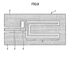
- FIG. 9 is a plan view showing an excitation structure according to a third embodiment of the present invention.
- a resonator 6 is a half-wavelength resonator. The central portion of the resonator 6 where current concentration is highest is placed close to a short-circuited end of an exciting line 4, to form an excitation structure giving the same advantage.
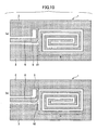
- Fig. 10 shows plan views of excitation structures according to a fourth embodiment of the present invention.
- the excitation structure shown in Fig. 10(a) is the same as that shown in Fig. 6(a) , except that a short-circuit portion of an exciting line 4 has a chamfered or truncated corner 51.
- the excitation structure shown in Fig. 10(b) is the same as that shown in Fig. 6(a) , except that a short-circuit portion of an exciting line 4 has a rounded corner 52.
- the current concentrating effect by the corners is decreased and lopsided current flows is eliminated, and therefore the circuit characteristics can be improved.
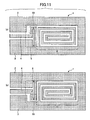
- Fig. 11 shows plan views of excitation structures according to a fifth embodiment of the present invention, in which excitation portions 5 are not L-shaped. As shown in Fig. 11(a), (b) , the excitation portions 5 have a folding back portion 53 which extends to the opposite side of a short-circuit portion of an exciting line 4. In these structures, a length ⁇ of the excitation portion 5 facing a resonator 6 is long and the coupling between the exciting line 4 and the resonator 6 is strengthened.
- Fig. 12 shows plan views of excitation structures according to a sixth embodiment of the present invention, in which excitation portions 5 are not L-shaped.
- the excitation portions 5 have a surrounding portion 54 between the folded corner of the excitation portion and a short-circuit portion connected to a ground conductor 2, 3.
- the surrounding portion 54 partially surrounds a part of a resonator 6 via a gap.
- the excitation portion 5 facing the resonator 6 is long and the coupling between the exciting line 4 and the resonator 6 is strengthened.
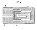
- Fig. 13 is a plan view showing an excitation structure according to a seventh embodiment of the present invention.
- This embodiment is different from the first-sixth embodiments in that an excitation portion 5 employs capacitive coupling instead of inductive coupling.
- the excitation portion 5 has a surrounding portion 55, which partially surrounds a part of a resonator 6 via a gap.
- the surrounding portion 55 has open ends.
- an exciting line 4 is provided at the center of a coplanar-waveguide circuit 1
- undesired transmission modes due to the exciting line 4 can be suppressed.
- the resonator 6 uses capacitive coupling, the excitation area on the coplanar-waveguide circuit 1 can be smaller by making the facing portion longer by means of the surrounding structure. Therefore, the circuit can be miniaturized, compared with Fig. 1 .
- the resonator 6 can be separated and independent due to the existence of the surrounding portion 55, and it is easy to independently adjust an external coupling strength.
- Figs. 14 shows plan views of filters 10 according to an eighth embodiment of the present invention.
- the filters 10 are four-pole bandpass filters having resonator exciting structures and four resonators (quarter-wavelength spiral resonator).
- resonator exciting structure an each end of exciting lines 4 is folded L-shape like and short-circuited to a ground conductor to form an excitation portion 5.
- the structures shown in Figs 14(a) ⁇ (f) have a variety of combinations of configurations of the excitation portion 5 and coupling methods between resonators 6.
- Fig. 15 is a plan view showing filters 10 according to a ninth embodiment of the present invention.
- the filters 10 may be a six-pole quasi-elliptic bandpass filter having exciting lines 4 and six resonators 6 (quarter-wavelength spiral resonator) .
- An each end of exciting lines 4 is folded L-shape like and short-circuited to a ground conductor to form an excitation portion 5.
- the structures shown in Figs 15(a), (b) have a variety of combinations of configurations of the excitation portion 5 and coupling methods between resonators 6.
- the resonator excitation structures of the bandpass filters shown in Figs. 14 and 15 are the same as that shown in Fig. 6 , and the resonator 6 is a quarter-wavelength spiral resonator.
- the resonator excitation structure may be the types shown in Figs. 10 ⁇ 13 , and the resonator 6 may be another type such as a quarter-wavelength lumped parameter type meandering resonator, a half-wavelength resonator or other resonator get the same characteristics.
- These structures are all included in the scope of the present invention. There are may combinations of the number of resonators and their coupling methods, and they are all included in the scope of the present invention.
Landscapes
- Physics & Mathematics (AREA)
- Electromagnetism (AREA)
- Control Of Motors That Do Not Use Commutators (AREA)
Abstract
A coupling structure for coupling to a circuit portion (6) in a coplanar-waveguide circuit (1) having ground conductors (2,3) at both sides is disclosed. A signal input/output line (4) is provided at the center of the coplanar-waveguide circuit; and an inductive coupling portion (5) having an end of the signal input/output line shortcircuited to one of the ground conductors and facing a part of the circuit portion via a first gap is also provided.
Description
- The present invention generally relates to a coupling structure, a resonator excitation structure and a filter mainly used for microwave or millimeter-wave band coplanar-waveguide circuits.
- In the prior art, two kinds of couplings are known as a resonator excitation structure at input/output of coplanar-waveguide circuits such as filters. One is capacitive coupling where an open end of an exciting line is close to a resonator. The other is inductive coupling where an exciting line is directly connected to a resonator.
-
Fig. 1 is a plan view of an excitation structure employing a conventional capacitive coupling (See Non-patent Document #1). A coplanar-waveguide circuit 1 includes anexciting line 4 longitudinally running at the center thereof. An end of theexciting line 4 is extended laterally like a T-shape. The T-shape portion of theexciting line 4 faces a T-shape portion of aresonator 6 via a gap to form anexcitation portion 5. The sides of thecoplanar plane circuit 1 are covered withcorresponding ground conductors -
Fig. 2 is a plan view of an excitation structure employing a conventional inductive coupling (See Non-patent Document #2). Anexciting line 4 is directly connected to a short-circuit portion between an end of aresonator 6 and aground conductor 3 to form anexcitation portion 5. -
Fig. 3 is a plan view of an excitation structure employing a conventional inductive coupling (See Non-patent Document #3). Anexciting line 4 is directly connected to an end of aresonator 6, and a cross-shape line is connected toground plates excitation portion 5. - [Non-patent Document #1] "A 5GHz Band Coplanar-Waveguide High Temperature superconducting Filter Employing T-shaped Input/Output Coupling Structure and Quarter-Wavelength Resonator" by Koizumi, Sato, Narahashi, Technical Report of IEICE, MW2004-25, pp. 55-60, May. 2004.
- [Non-patent Document #2] "Design of a 5GHz Bandpass Filter Using CPW Quarter-Wavelength Spiral Resonators" by Kawaguchi, Ma, Kobayashi, Proceedings of the 2004 IEICE Society Conference, C-2-81, Nov. 2004.
- [Non-patent Document #3] "Design of a 5GHz Interdigital Bandpass Filter Using CPW Quarter-Wavelength Resonators" by Kawaguchi, Ma, Kobayashi, Proceedings of the 2004 IEICE Society Conference, C-2-80, Nov. 2004.
- The above mentioned conventional excitation structures shown in
Figs. 1∼3 have problems discussed below. - In the resonator excitation structure using capacitive coupling as shown in
Fig. 1 , its external coupling is in general weaker than that in a resonator excitation structure using inductive coupling. When designing bandpass filters using capacitive coupling, in order to obtain a desired external coupling strength, the open end portion of the exciting line must be placed near a portion of the resonator where charges are concentrated. However, if such a charge concentrated portion is not at an outer area, the length of the exciting line must be long enough to ensure a sufficient external coupling strength. That enlarges the excitation structure area of the planar circuit substrate, adversely affects a next stage resonator, and degrades entire circuit characteristics, which are problems. - On the other hand, in a resonator excitation structure using direct connected inductive couplings as shown in
Fig. 2 or3 , its external coupling is too strong. Accordingly an exciting line must be directed coupled to the resonator near a short-circuit portion in case of quarter-wavelength resonators, and it is difficult to place the exciting line near the center of plane circuit substrate. When a housing can be considered to be a cut-off waveguide, undesired transmission modes or propagation modes are strongly excited and the circuit characteristics are degraded. - In addition, when adjusting the external coupling strength after manufacturing a planar circuit substrate and circuit pattern, such adjustment also affects the resonant frequency of the resonator. Therefore, it is impossible to independently adjust the external coupling parameter only. As an example explaining this problem,
Fig. 4 shows a resonator excitation structure in which an exciting line is directly connected to quarter-wavelength spiral resonator to form inductive coupling. By removing an adjusting portion 7 (indicated by hatched lines) of aground conductor 2 after manufacturing a circuit pattern, it is possible to increase a gap width g between theground conductor 2 and aresonator 6 and increase its external Q or weaken external coupling strength.Fig. 5 is a graph showing that the external Q and the resonant frequency of theresonator 6 vary with respect to the gap width g. As clearly shown inFig. 5 , the increase of the gap width g increases not only the external Q but also the resonant frequency of theresonator 6. - Although the above explanation is given about the excitation structure of resonators, these problems may occur at a connecting portion between any circuit portions and signal input/output lines in planar circuits.
- The present invention may provide a coupling structure, a resonator excitation structure and a filter for coplanar-waveguide circuit, in which undesired transmission modes due to signal input/output lines can be suppressed, the coupling area on the coplanar-waveguide circuit substrate is miniaturized, and parameters such as an external Q can be independently adjusted even after manufacturing the circuit pattern.
- In a preferred embodiment of the present invention is provided a coupling structure for coupling to a circuit portion (6) in a coplanar plane circuit (1) having ground conductors (2, 3) at both sides, comprising:
- a signal input/output line (4) provided at the center of the coplanar-waveguide circuit; and
- an inductive coupling portion (5) having an end of the signal input/output line short-circuited to one of the ground conductors and facing a part of the circuit portion via a first gap (α).
- In another embodiment of the present invention is provided a coupling structure for coupling to a circuit portion (6) in a coplanar-waveguide circuit (1) having ground conductors (2, 3) at both sides, comprising:
- a signal input/output line (4) provided at the center of the coplanar-waveguide circuit; and
- a capacitive coupling portion (5) having a surrounding portion (55) at an end of the signal input/output line, the surrounding portion partly surrounding and facing a part of the circuit portion (6) via a first gap.
- In further another embodiment of the present invention is provided a resonator excitation structure for exciting a resonator in a coplanar-waveguide circuit (1) having ground conductors (2, 3) at both sides, comprising:
- an exciting line (4) provided at the center of the coplanar-waveguide circuit; and
- an excitation portion (5) having an end of the exciting line short-circuited to one of the ground conductors and facing a part of the resonator via a first gap (α).
- In further another embodiment of the present invention is provided a filter (10) having one or more resonators (6) in a coplanar-waveguide circuit having ground conductors (2, 3) at both sides, comprising:
- an exciting line (4) provided at the center of the coplanar-waveguide circuit; and
- an excitation portion (5) having an end of the exciting line short-circuited to one of the ground conductors and facing a part of the first or last one of the resonators via a first gap (α).
- According to the embodiments of the present invention, a coupling structure, a resonator excitation structure and a filter for coplanar-waveguide circuits are provided in which undesired transmission modes due to signal input/output lines can be suppressed, the coupling area on the coplanar-waveguide circuit substrate is miniaturized, parameters such as an external Q can be independently adjusted even after manufacturing the circuit pattern. Especially in microwave or millimeter-wave band coplanar-waveguide circuits housed in a shielded waveguide, it is possible to form a miniaturized excitation structure suppressing undesired transmission modes due to signal input/output lines, and it is possible to adjust an external coupling strength only, without changing other parameters to obtain desired circuit characteristics.
-
-
Fig. 1 is a plan view of an excitation structure employing a conventional capacitive coupling; -
Fig. 2 is a plan view of an excitation structure employing a conventional inductive coupling; -
Fig. 3 is a plan view of an excitation structure employing a conventional inductive coupling; -
Fig. 4 shows an adjustment method in a resonator excitation structure with a conventional inductive coupling; -
Fig. 5 is a graph showing that the external Q and the resonant frequency of the resonator shown inFig. 4 vary with respect to the gap width g; -
Fig. 6 shows plan views of excitation structures according to a first embodiment of the present invention; -
Fig. 7 shows two graphs each showing that the external Q and the resonant frequency of the resonator shown inFig. 6 vary with respect to the gap width g; -
Fig. 8 shows plan views of excitation structures according to a second embodiment of the present invention; -
Fig. 9 is a plan view of showing an excitation structure according to a third embodiment of the present invention; -
Fig. 10 is a plan view showing excitation structures according to a fourth embodiment of the present invention; -
Fig. 11 is a plan view showing excitation structures according to a fifth embodiment of the present invention; -
Fig. 12 is a plan view showing excitation structures according to a sixth embodiment of the present invention; -
Fig. 13 is a plan view showing excitation structures according to a seventh embodiment of the present invention; -
Fig. 14 is a plan view showing excitation structures according to an eighth embodiment of the present invention; and -
Fig. 15 is a plan view showing excitation structures according to a ninth embodiment of the present invention. - The following is a description of embodiments of the present invention, with reference to the accompanying drawings.
- Throughout all the figures, members and parts having the same or similar functions are assigned the same or similar reference signs, and redundant explanations are omitted.
-
Fig. 6 shows plan views of an excitation structure according to a first embodiment of the present invention. A coplanar-waveguide circuit 1 shown inFig. 6(a) hasground conductors exciting line 4 as a signal input/output line is provided at the central area of thecoplanar plane circuit 1 in order not to generate undesired transmission modes or propagation modes in a shielded waveguide housing the circuit substrate. In this embodiment, a circuit to which theexciting line 4 is connected is a quarter-wavelength spiral resonator 6. An end of theexciting line 4 is folded L-shape like and short-circuited to theground conductor 2 at non-short-circuit side of theresonator 6. This short-circuit line faces a charge concentrated portion of theresonator 6 via a gap having a width α, to form anexcitation portion 5 using inductive coupling. A strength of the external coupling is determined by factors such as the gap width α, a length β of the short-circuit line of theexciting line 4, and a distance s between the short-circuit line of theexciting line 4 and theground conductor 2. - An example shown in
Fig. 6(b) is different from that inFig. 6(a) in that an end of anexciting line 4 is folded to a short-circuit side of aresonator 6 to form anexcitation portion 5. - When it is required to adjust the external coupling strength independently from the resonant frequency of the
resonator 6 after manufacturing the circuit pattern, an adjustment portion 7 (indicated by hatched lines) of theground conductors -
Figs. 7(a), (b) are graphs showing that the external Q and the resonant frequency of theresonators 6 shown inFigs. 6(a), (b) respectively vary with respect to the gap width g. As clearly shown inFigs. 7(a), (b) , the resonant frequency of theresonators 6 does not substantially change due to the variation of the gap width s between the short-circuit line and the ground conductor, which makes the external Q change. In general, the narrower the width of the short-circuit line is, the larger the variation of the external Q becomes. Therefore, the width of the short-circuit line can be adequately designed, in order to obtain a desired variation by removing the ground conductor and widening the gap width s by a certain extent. -
Fig. 8 shows plan views of excitation structures according to a second embodiment of the present invention.Resonators 6 are quarter-wavelength lumped-parameter type meandering resonators. In the resonant excitation structure shown inFig. 8 (a) , an end of anexciting line 4 is folded L-shape like and short-circuited to aground conductor 2 at non-short-circuit side of theresonator 6 to form anexcitation portion 5. In the resonant excitation structure shown inFig. 8 (b) , an end of anexciting line 4 is folded L-shape like a short-circuited to aground conductor 3 at a short-circuit side of theresonator 6 to form anexcitation portion 5. These structures have the same advantage as the above-explained structures shown inFigs. 6(a), (b) . - The
resonator 6 may be any types of quarter-wavelength resonators, as long as a short-circuit portion thereof is placed close to a short-circuited end of anexciting line 4. In this manner, a variety of excitation structures having the same advantage are obtained, which are all included in the scope of the present invention. -
Fig. 9 is a plan view showing an excitation structure according to a third embodiment of the present invention. Aresonator 6 is a half-wavelength resonator. The central portion of theresonator 6 where current concentration is highest is placed close to a short-circuited end of anexciting line 4, to form an excitation structure giving the same advantage. -
Fig. 10 shows plan views of excitation structures according to a fourth embodiment of the present invention. The excitation structure shown inFig. 10(a) is the same as that shown inFig. 6(a) , except that a short-circuit portion of anexciting line 4 has a chamfered ortruncated corner 51. The excitation structure shown inFig. 10(b) is the same as that shown inFig. 6(a) , except that a short-circuit portion of anexciting line 4 has a roundedcorner 52. In these structures, the current concentrating effect by the corners is decreased and lopsided current flows is eliminated, and therefore the circuit characteristics can be improved. -
Fig. 11 shows plan views of excitation structures according to a fifth embodiment of the present invention, in whichexcitation portions 5 are not L-shaped. As shown inFig. 11(a), (b) , theexcitation portions 5 have a folding backportion 53 which extends to the opposite side of a short-circuit portion of anexciting line 4. In these structures, a length β of theexcitation portion 5 facing aresonator 6 is long and the coupling between theexciting line 4 and theresonator 6 is strengthened. -
Fig. 12 shows plan views of excitation structures according to a sixth embodiment of the present invention, in whichexcitation portions 5 are not L-shaped. As shown inFigs. 12(a), (b) , theexcitation portions 5 have a surroundingportion 54 between the folded corner of the excitation portion and a short-circuit portion connected to aground conductor portion 54 partially surrounds a part of aresonator 6 via a gap. In these structures also, theexcitation portion 5 facing theresonator 6 is long and the coupling between theexciting line 4 and theresonator 6 is strengthened. -
Fig. 13 is a plan view showing an excitation structure according to a seventh embodiment of the present invention. This embodiment is different from the first-sixth embodiments in that anexcitation portion 5 employs capacitive coupling instead of inductive coupling. Theexcitation portion 5 has a surroundingportion 55, which partially surrounds a part of aresonator 6 via a gap. The surroundingportion 55 has open ends. In this case also, since anexciting line 4 is provided at the center of a coplanar-waveguide circuit 1, undesired transmission modes due to theexciting line 4 can be suppressed. Although theresonator 6 uses capacitive coupling, the excitation area on the coplanar-waveguide circuit 1 can be smaller by making the facing portion longer by means of the surrounding structure. Therefore, the circuit can be miniaturized, compared withFig. 1 . Theresonator 6 can be separated and independent due to the existence of the surroundingportion 55, and it is easy to independently adjust an external coupling strength. -
Figs. 14 shows plan views offilters 10 according to an eighth embodiment of the present invention. Thefilters 10 are four-pole bandpass filters having resonator exciting structures and four resonators (quarter-wavelength spiral resonator). In the resonator exciting structure, an each end ofexciting lines 4 is folded L-shape like and short-circuited to a ground conductor to form anexcitation portion 5. The structures shown inFigs 14(a)∼(f) have a variety of combinations of configurations of theexcitation portion 5 and coupling methods betweenresonators 6. -
Fig. 15 is a plan view showing filters 10 according to a ninth embodiment of the present invention. Thefilters 10 may be a six-pole quasi-elliptic bandpass filter havingexciting lines 4 and six resonators 6 (quarter-wavelength spiral resonator) . An each end ofexciting lines 4 is folded L-shape like and short-circuited to a ground conductor to form anexcitation portion 5. The structures shown inFigs 15(a), (b) have a variety of combinations of configurations of theexcitation portion 5 and coupling methods betweenresonators 6. - The resonator excitation structures of the bandpass filters shown in
Figs. 14 and15 are the same as that shown inFig. 6 , and theresonator 6 is a quarter-wavelength spiral resonator. However, the resonator excitation structure may be the types shown inFigs. 10∼13 , and theresonator 6 may be another type such as a quarter-wavelength lumped parameter type meandering resonator, a half-wavelength resonator or other resonator get the same characteristics. These structures are all included in the scope of the present invention. There are may combinations of the number of resonators and their coupling methods, and they are all included in the scope of the present invention.
Claims (7)
- A coplanar waveguide circuit (1) comprising:a planar, spiral resonator portion (6);ground conductors (2, 3) extending along each respective side between first and second ends of the circuit and joined together at the first end, surrounding on three sides the resonator portion (6);an elongate space along the centre of the circuit (1) between the ground conductors and between the second end and the resonator portion;an elongate signal input/output line (4) extending longitudinally within the elongate space, and centrally of the circuit (1), from the second end to a longitudinal position which is spaced by a first gap (α) from the resonator portion;an elongate inductive coupling portion (5) of the signal input/output line (4) extending transversely, as a folded end thereof, from the longitudinal position to a first one of the ground conductors (2, 3) and spaced by the said first gap (α) from a transverse edge of the resonator portion (6) opposed to the first end of the circuit (1), the inductive coupling portion (5) being connected to one of the ground conductors (2, 3);a further space extending transversely between the first ground conductor (2, 3) and the said elongate space and longitudinally, as a second gap (s), between a transverse edge of a shoulder on the first conductor and the inductive coupling portion (5);the length of the first ground conductor between the second end and the shoulder being greater than the second gap (s);wherein the external coupling strength of the circuit (1) is adjustable independently of the resonant frequency of the resonator portion (6) by selectively removing a portion (7) of the first ground conductor from the shoulder to lengthen the second gap (s).
- A circuit according to Claim 1, wherein the inductive coupling portion (5) is connected to the first ground conductor.
- A circuit according to Claim 1, wherein the inductive coupling portion (5) is connected to the second ground conductor by way of a bend (53, Figure 11).
- A circuit according to Claim 2, wherein a corner (51, 52) on the fold of the signal input/output line (4) is chamfered or rounded.
- A circuit according to any preceding claim, wherein the spiral resonator portion (6) is connected to the first ground conductor.
- A circuit according to any of Claims 1 to 4, wherein the spiral resonator portion (6) is connected to the second ground conductor.
- A circuit according to any preceding claim, wherein the spiral resonator portion (6) is a quarter-wavelength spiral resonator.
Applications Claiming Priority (2)
| Application Number | Priority Date | Filing Date | Title |
|---|---|---|---|
| JP2005033336A JP4287388B2 (en) | 2005-02-09 | 2005-02-09 | Coplanar planar in-circuit coupling structure, resonator excitation structure and filter |
| EP06250713A EP1691443B1 (en) | 2005-02-09 | 2006-02-09 | Coupling structure, resonator excitation structure and filter for coplanar-waveguide circuit |
Related Parent Applications (1)
| Application Number | Title | Priority Date | Filing Date |
|---|---|---|---|
| EP06250713A Division EP1691443B1 (en) | 2005-02-09 | 2006-02-09 | Coupling structure, resonator excitation structure and filter for coplanar-waveguide circuit |
Publications (1)
| Publication Number | Publication Date |
|---|---|
| EP2065964A1 true EP2065964A1 (en) | 2009-06-03 |
Family
ID=36273524
Family Applications (2)
| Application Number | Title | Priority Date | Filing Date |
|---|---|---|---|
| EP06250713A Expired - Fee Related EP1691443B1 (en) | 2005-02-09 | 2006-02-09 | Coupling structure, resonator excitation structure and filter for coplanar-waveguide circuit |
| EP09003263A Withdrawn EP2065964A1 (en) | 2005-02-09 | 2006-02-09 | Coupling structure, resonator excitation structure and filter for coplanar-waveguide circuit |
Family Applications Before (1)
| Application Number | Title | Priority Date | Filing Date |
|---|---|---|---|
| EP06250713A Expired - Fee Related EP1691443B1 (en) | 2005-02-09 | 2006-02-09 | Coupling structure, resonator excitation structure and filter for coplanar-waveguide circuit |
Country Status (6)
| Country | Link |
|---|---|
| US (1) | US7397331B2 (en) |
| EP (2) | EP1691443B1 (en) |
| JP (1) | JP4287388B2 (en) |
| KR (1) | KR100820285B1 (en) |
| CN (1) | CN100466374C (en) |
| DE (1) | DE602006008998D1 (en) |
Families Citing this family (8)
| Publication number | Priority date | Publication date | Assignee | Title |
|---|---|---|---|---|
| KR100806389B1 (en) * | 2006-01-09 | 2008-02-27 | 삼성전자주식회사 | PARALLE COUPLED CPW LINE Filter |
| US7649431B2 (en) * | 2006-10-27 | 2010-01-19 | Samsung Electro-Mechanics Co., Ltd. | Band pass filter |
| JP4728994B2 (en) * | 2007-03-29 | 2011-07-20 | 株式会社エヌ・ティ・ティ・ドコモ | Coplanar resonator and coplanar filter using the same |
| JP4758942B2 (en) | 2007-05-10 | 2011-08-31 | 株式会社エヌ・ティ・ティ・ドコモ | Dual band resonator and dual band filter |
| WO2009132044A1 (en) * | 2008-04-21 | 2009-10-29 | Spx Corporation | Phased-array antenna filter and diplexer for a super economical broadcast system |
| WO2014171091A1 (en) | 2013-04-18 | 2014-10-23 | パナソニック株式会社 | Resonant coupler |
| CN105072852B (en) * | 2015-07-31 | 2017-11-17 | 中国科学院国家天文台 | The universal architecture of a kind of electronic equipment protection |
| CN112467327B (en) * | 2020-11-27 | 2022-02-01 | 江苏亨通太赫兹技术有限公司 | Waveguide-coplanar waveguide transition structure based on electromagnetic band gap and back-to-back structure |
Citations (5)
| Publication number | Priority date | Publication date | Assignee | Title |
|---|---|---|---|---|
| US3451015A (en) * | 1966-03-21 | 1969-06-17 | Gen Dynamics Corp | Microwave stripline filter |
| US3745489A (en) * | 1972-05-01 | 1973-07-10 | Stanford Research Inst | Microwave and uhf filters using discrete hairpin resonators |
| EP0068345A1 (en) * | 1981-06-25 | 1983-01-05 | Communications Satellite Corporation | Symmetrical coupled line coplanar waveguide filter |
| EP0431234A1 (en) * | 1989-12-07 | 1991-06-12 | ELETTRONICA S.p.a. | Band-pass speedy tunable filter of the combline-type |
| EP1562255A1 (en) * | 2004-02-03 | 2005-08-10 | NTT DoCoMo, Inc. | Coplanar filter |
Family Cites Families (1)
| Publication number | Priority date | Publication date | Assignee | Title |
|---|---|---|---|---|
| JP3319377B2 (en) * | 1998-01-30 | 2002-08-26 | 株式会社村田製作所 | Coplanar line filter and duplexer |
-
2005
- 2005-02-09 JP JP2005033336A patent/JP4287388B2/en not_active Expired - Fee Related
-
2006
- 2006-02-09 KR KR1020060012526A patent/KR100820285B1/en not_active Expired - Fee Related
- 2006-02-09 US US11/349,775 patent/US7397331B2/en not_active Expired - Fee Related
- 2006-02-09 CN CNB2006100073510A patent/CN100466374C/en not_active Expired - Fee Related
- 2006-02-09 EP EP06250713A patent/EP1691443B1/en not_active Expired - Fee Related
- 2006-02-09 EP EP09003263A patent/EP2065964A1/en not_active Withdrawn
- 2006-02-09 DE DE602006008998T patent/DE602006008998D1/en not_active Expired - Lifetime
Patent Citations (5)
| Publication number | Priority date | Publication date | Assignee | Title |
|---|---|---|---|---|
| US3451015A (en) * | 1966-03-21 | 1969-06-17 | Gen Dynamics Corp | Microwave stripline filter |
| US3745489A (en) * | 1972-05-01 | 1973-07-10 | Stanford Research Inst | Microwave and uhf filters using discrete hairpin resonators |
| EP0068345A1 (en) * | 1981-06-25 | 1983-01-05 | Communications Satellite Corporation | Symmetrical coupled line coplanar waveguide filter |
| EP0431234A1 (en) * | 1989-12-07 | 1991-06-12 | ELETTRONICA S.p.a. | Band-pass speedy tunable filter of the combline-type |
| EP1562255A1 (en) * | 2004-02-03 | 2005-08-10 | NTT DoCoMo, Inc. | Coplanar filter |
Non-Patent Citations (3)
| Title |
|---|
| KAWAGUCHI, MA, KOBAYASHI: "Design of a 5GHz Bandpass Filter Using CPW Quarter-Wavelength Spiral Resonators", PROCEEDINGS OF THE 2004 IEICE SOCIETY CONFERENCE, vol. C-2-81, November 2004 (2004-11-01) |
| KAWAGUCHI, MA, KOBAYASHI: "Design of a 5GHz Interdigital Bandpass Filter Using CPW Quarter-Wavelength Resonators", PROCEEDINGS OF THE 2004 IEICE SOCIETY CONFERENCE, vol. C-2-80, November 2004 (2004-11-01) |
| KOIZUMI, SATO; NARAHASHI: "A 5GHz Band Coplanar-Waveguide High Temperature superconducting Filter Employing T-shaped Input/Output Coupling Structure and Quarter-Wavelength Resonator", TECHNICAL REPORT OF IEICE, MW2004-25, May 2004 (2004-05-01), pages 55 - 60 |
Also Published As
| Publication number | Publication date |
|---|---|
| JP4287388B2 (en) | 2009-07-01 |
| EP1691443B1 (en) | 2009-09-09 |
| DE602006008998D1 (en) | 2009-10-22 |
| JP2006222664A (en) | 2006-08-24 |
| CN1825692A (en) | 2006-08-30 |
| EP1691443A1 (en) | 2006-08-16 |
| CN100466374C (en) | 2009-03-04 |
| KR100820285B1 (en) | 2008-04-07 |
| US20060193559A1 (en) | 2006-08-31 |
| US7397331B2 (en) | 2008-07-08 |
| KR20060090620A (en) | 2006-08-14 |
Similar Documents
| Publication | Publication Date | Title |
|---|---|---|
| EP1990863B1 (en) | Dual band resonator and dual band filter | |
| EP0730318A2 (en) | Strip dual mode loop resonator for resonating microwave in dual mode and band-pass filter composed of the resonators | |
| WO2012057708A1 (en) | Multiple-mode filter for radio frequency integrated circuits | |
| US20050206481A1 (en) | Filter | |
| EP1691443B1 (en) | Coupling structure, resonator excitation structure and filter for coplanar-waveguide circuit | |
| EP0783188B1 (en) | Dielectric filter | |
| JP5733763B2 (en) | Multiband bandpass filter | |
| EP1976052A1 (en) | Coplanar waveguide resonator and coplanar waveguide filter using the same | |
| US7764147B2 (en) | Coplanar resonator and filter using the same | |
| US20160240905A1 (en) | Hybrid folded rectangular waveguide filter | |
| EP1172879B1 (en) | Dual-mode band-pass filter | |
| US7274273B2 (en) | Dielectric resonator device, dielectric filter, duplexer, and high-frequency communication apparatus | |
| JP3723284B2 (en) | High frequency filter | |
| JP6265460B2 (en) | Dual band resonator and dual band bandpass filter using the same | |
| US6535078B1 (en) | Dielectric filter, dielectric duplexer, and communication system | |
| JP6262437B2 (en) | Polarized bandpass filter | |
| KR19980079948A (en) | Dielectric Filters, Dielectric Duplexers and Manufacturing Methods Thereof | |
| US6828880B2 (en) | Bandpass filter | |
| US6249195B1 (en) | Dielectric filter, dielectric duplexer, and transceiver having circular and polygonal electrode openings | |
| JP4411315B2 (en) | Band stop filter | |
| US7479856B2 (en) | High-frequency filter using coplanar line resonator | |
| JP2007201764A (en) | filter | |
| US7482898B2 (en) | Dielectric filter, dielectric duplexer, and communication apparatus | |
| JP2003304103A (en) | Bandpass filter | |
| US20050162241A1 (en) | Variable-frequency high frequency filter |
Legal Events
| Date | Code | Title | Description |
|---|---|---|---|
| PUAI | Public reference made under article 153(3) epc to a published international application that has entered the european phase |
Free format text: ORIGINAL CODE: 0009012 |
|
| STAA | Information on the status of an ep patent application or granted ep patent |
Free format text: STATUS: THE APPLICATION HAS BEEN WITHDRAWN |
|
| 17P | Request for examination filed |
Effective date: 20090311 |
|
| AC | Divisional application: reference to earlier application |
Ref document number: 1691443 Country of ref document: EP Kind code of ref document: P |
|
| AK | Designated contracting states |
Kind code of ref document: A1 Designated state(s): DE GB |
|
| 18W | Application withdrawn |
Effective date: 20090504 |