EP2065698B1 - Puce destinée à l'analyse d'un milieu à l'aide d'un émetteur de lumière organique intégré et procédé pour fabriquer une telle puce - Google Patents
Puce destinée à l'analyse d'un milieu à l'aide d'un émetteur de lumière organique intégré et procédé pour fabriquer une telle puce Download PDFInfo
- Publication number
- EP2065698B1 EP2065698B1 EP08020309.4A EP08020309A EP2065698B1 EP 2065698 B1 EP2065698 B1 EP 2065698B1 EP 08020309 A EP08020309 A EP 08020309A EP 2065698 B1 EP2065698 B1 EP 2065698B1
- Authority
- EP
- European Patent Office
- Prior art keywords
- chip
- photodetector
- organic light
- light emitter
- emitter
- Prior art date
- Legal status (The legal status is an assumption and is not a legal conclusion. Google has not performed a legal analysis and makes no representation as to the accuracy of the status listed.)
- Active
Links
- 238000000034 method Methods 0.000 title claims description 9
- 238000004519 manufacturing process Methods 0.000 title claims description 6
- 230000008569 process Effects 0.000 title description 6
- 239000000758 substrate Substances 0.000 claims description 36
- 230000003595 spectral effect Effects 0.000 claims description 33
- 230000035945 sensitivity Effects 0.000 claims description 15
- 229910052751 metal Inorganic materials 0.000 claims description 14
- 239000002184 metal Substances 0.000 claims description 14
- 230000005855 radiation Effects 0.000 claims description 12
- 239000004065 semiconductor Substances 0.000 claims description 12
- 238000011156 evaluation Methods 0.000 claims description 8
- 238000013086 organic photovoltaic Methods 0.000 claims description 3
- 239000010410 layer Substances 0.000 description 65
- 239000000126 substance Substances 0.000 description 13
- 101000864342 Homo sapiens Tyrosine-protein kinase BTK Proteins 0.000 description 10
- 102100029823 Tyrosine-protein kinase BTK Human genes 0.000 description 10
- 230000000052 comparative effect Effects 0.000 description 10
- 230000010354 integration Effects 0.000 description 10
- 239000000463 material Substances 0.000 description 9
- 238000004458 analytical method Methods 0.000 description 8
- 239000012044 organic layer Substances 0.000 description 8
- 101000621427 Homo sapiens Wiskott-Aldrich syndrome protein Proteins 0.000 description 7
- XUIMIQQOPSSXEZ-UHFFFAOYSA-N Silicon Chemical compound [Si] XUIMIQQOPSSXEZ-UHFFFAOYSA-N 0.000 description 7
- 102100023034 Wiskott-Aldrich syndrome protein Human genes 0.000 description 7
- 230000003287 optical effect Effects 0.000 description 7
- 210000002966 serum Anatomy 0.000 description 7
- 229910052710 silicon Inorganic materials 0.000 description 7
- 238000010521 absorption reaction Methods 0.000 description 6
- 239000003086 colorant Substances 0.000 description 6
- 238000013461 design Methods 0.000 description 6
- 238000002161 passivation Methods 0.000 description 6
- 239000010703 silicon Substances 0.000 description 6
- 230000000694 effects Effects 0.000 description 5
- 238000005516 engineering process Methods 0.000 description 5
- 238000005286 illumination Methods 0.000 description 5
- 238000009413 insulation Methods 0.000 description 5
- 239000000523 sample Substances 0.000 description 5
- 230000008901 benefit Effects 0.000 description 4
- 238000001914 filtration Methods 0.000 description 4
- 239000011159 matrix material Substances 0.000 description 4
- 238000000018 DNA microarray Methods 0.000 description 3
- 230000004888 barrier function Effects 0.000 description 3
- 239000003153 chemical reaction reagent Substances 0.000 description 3
- 238000012545 processing Methods 0.000 description 3
- 239000002344 surface layer Substances 0.000 description 3
- 238000004847 absorption spectroscopy Methods 0.000 description 2
- 230000008033 biological extinction Effects 0.000 description 2
- 210000004369 blood Anatomy 0.000 description 2
- 239000008280 blood Substances 0.000 description 2
- 239000000470 constituent Substances 0.000 description 2
- 238000000151 deposition Methods 0.000 description 2
- 230000008021 deposition Effects 0.000 description 2
- 238000001514 detection method Methods 0.000 description 2
- 230000010365 information processing Effects 0.000 description 2
- 239000007788 liquid Substances 0.000 description 2
- 238000005259 measurement Methods 0.000 description 2
- 238000001465 metallisation Methods 0.000 description 2
- 239000000615 nonconductor Substances 0.000 description 2
- 230000005693 optoelectronics Effects 0.000 description 2
- 239000011368 organic material Substances 0.000 description 2
- 230000009467 reduction Effects 0.000 description 2
- 230000002123 temporal effect Effects 0.000 description 2
- 239000012780 transparent material Substances 0.000 description 2
- 240000003517 Elaeocarpus dentatus Species 0.000 description 1
- 229910001218 Gallium arsenide Inorganic materials 0.000 description 1
- 241000557769 Iodes Species 0.000 description 1
- 238000000862 absorption spectrum Methods 0.000 description 1
- 239000013543 active substance Substances 0.000 description 1
- 239000012491 analyte Substances 0.000 description 1
- 230000015572 biosynthetic process Effects 0.000 description 1
- 239000000969 carrier Substances 0.000 description 1
- 230000008859 change Effects 0.000 description 1
- 238000004040 coloring Methods 0.000 description 1
- 238000010276 construction Methods 0.000 description 1
- 230000008878 coupling Effects 0.000 description 1
- 238000010168 coupling process Methods 0.000 description 1
- 238000005859 coupling reaction Methods 0.000 description 1
- 239000003989 dielectric material Substances 0.000 description 1
- 239000002019 doping agent Substances 0.000 description 1
- 238000005401 electroluminescence Methods 0.000 description 1
- 210000003608 fece Anatomy 0.000 description 1
- 239000007850 fluorescent dye Substances 0.000 description 1
- 239000011521 glass Substances 0.000 description 1
- 238000003384 imaging method Methods 0.000 description 1
- AMGQUBHHOARCQH-UHFFFAOYSA-N indium;oxotin Chemical compound [In].[Sn]=O AMGQUBHHOARCQH-UHFFFAOYSA-N 0.000 description 1
- 239000004615 ingredient Substances 0.000 description 1
- 238000011835 investigation Methods 0.000 description 1
- PNDPGZBMCMUPRI-UHFFFAOYSA-N iodine Chemical compound II PNDPGZBMCMUPRI-UHFFFAOYSA-N 0.000 description 1
- 238000002955 isolation Methods 0.000 description 1
- 239000010871 livestock manure Substances 0.000 description 1
- 238000002493 microarray Methods 0.000 description 1
- 238000012805 post-processing Methods 0.000 description 1
- 230000006798 recombination Effects 0.000 description 1
- 238000005215 recombination Methods 0.000 description 1
- 210000002023 somite Anatomy 0.000 description 1
- 230000003068 static effect Effects 0.000 description 1
- 239000010409 thin film Substances 0.000 description 1
- 230000003313 weakening effect Effects 0.000 description 1
Images


Classifications
-
- G—PHYSICS
- G01—MEASURING; TESTING
- G01N—INVESTIGATING OR ANALYSING MATERIALS BY DETERMINING THEIR CHEMICAL OR PHYSICAL PROPERTIES
- G01N21/00—Investigating or analysing materials by the use of optical means, i.e. using sub-millimetre waves, infrared, visible or ultraviolet light
- G01N21/62—Systems in which the material investigated is excited whereby it emits light or causes a change in wavelength of the incident light
- G01N21/63—Systems in which the material investigated is excited whereby it emits light or causes a change in wavelength of the incident light optically excited
- G01N21/64—Fluorescence; Phosphorescence
- G01N21/6408—Fluorescence; Phosphorescence with measurement of decay time, time resolved fluorescence
-
- G—PHYSICS
- G01—MEASURING; TESTING
- G01J—MEASUREMENT OF INTENSITY, VELOCITY, SPECTRAL CONTENT, POLARISATION, PHASE OR PULSE CHARACTERISTICS OF INFRARED, VISIBLE OR ULTRAVIOLET LIGHT; COLORIMETRY; RADIATION PYROMETRY
- G01J3/00—Spectrometry; Spectrophotometry; Monochromators; Measuring colours
- G01J3/02—Details
- G01J3/0256—Compact construction
- G01J3/0259—Monolithic
-
- G—PHYSICS
- G01—MEASURING; TESTING
- G01J—MEASUREMENT OF INTENSITY, VELOCITY, SPECTRAL CONTENT, POLARISATION, PHASE OR PULSE CHARACTERISTICS OF INFRARED, VISIBLE OR ULTRAVIOLET LIGHT; COLORIMETRY; RADIATION PYROMETRY
- G01J3/00—Spectrometry; Spectrophotometry; Monochromators; Measuring colours
- G01J3/02—Details
- G01J3/10—Arrangements of light sources specially adapted for spectrometry or colorimetry
-
- G—PHYSICS
- G01—MEASURING; TESTING
- G01J—MEASUREMENT OF INTENSITY, VELOCITY, SPECTRAL CONTENT, POLARISATION, PHASE OR PULSE CHARACTERISTICS OF INFRARED, VISIBLE OR ULTRAVIOLET LIGHT; COLORIMETRY; RADIATION PYROMETRY
- G01J3/00—Spectrometry; Spectrophotometry; Monochromators; Measuring colours
- G01J3/28—Investigating the spectrum
- G01J3/44—Raman spectrometry; Scattering spectrometry ; Fluorescence spectrometry
- G01J3/4406—Fluorescence spectrometry
-
- G—PHYSICS
- G01—MEASURING; TESTING
- G01N—INVESTIGATING OR ANALYSING MATERIALS BY DETERMINING THEIR CHEMICAL OR PHYSICAL PROPERTIES
- G01N21/00—Investigating or analysing materials by the use of optical means, i.e. using sub-millimetre waves, infrared, visible or ultraviolet light
- G01N21/17—Systems in which incident light is modified in accordance with the properties of the material investigated
- G01N21/25—Colour; Spectral properties, i.e. comparison of effect of material on the light at two or more different wavelengths or wavelength bands
- G01N21/31—Investigating relative effect of material at wavelengths characteristic of specific elements or molecules, e.g. atomic absorption spectrometry
-
- G—PHYSICS
- G01—MEASURING; TESTING
- G01N—INVESTIGATING OR ANALYSING MATERIALS BY DETERMINING THEIR CHEMICAL OR PHYSICAL PROPERTIES
- G01N21/00—Investigating or analysing materials by the use of optical means, i.e. using sub-millimetre waves, infrared, visible or ultraviolet light
- G01N21/62—Systems in which the material investigated is excited whereby it emits light or causes a change in wavelength of the incident light
- G01N21/63—Systems in which the material investigated is excited whereby it emits light or causes a change in wavelength of the incident light optically excited
- G01N21/64—Fluorescence; Phosphorescence
- G01N21/645—Specially adapted constructive features of fluorimeters
- G01N21/6452—Individual samples arranged in a regular 2D-array, e.g. multiwell plates
- G01N21/6454—Individual samples arranged in a regular 2D-array, e.g. multiwell plates using an integrated detector array
-
- B—PERFORMING OPERATIONS; TRANSPORTING
- B01—PHYSICAL OR CHEMICAL PROCESSES OR APPARATUS IN GENERAL
- B01L—CHEMICAL OR PHYSICAL LABORATORY APPARATUS FOR GENERAL USE
- B01L3/00—Containers or dishes for laboratory use, e.g. laboratory glassware; Droppers
- B01L3/50—Containers for the purpose of retaining a material to be analysed, e.g. test tubes
- B01L3/502—Containers for the purpose of retaining a material to be analysed, e.g. test tubes with fluid transport, e.g. in multi-compartment structures
- B01L3/5027—Containers for the purpose of retaining a material to be analysed, e.g. test tubes with fluid transport, e.g. in multi-compartment structures by integrated microfluidic structures, i.e. dimensions of channels and chambers are such that surface tension forces are important, e.g. lab-on-a-chip
- B01L3/502707—Containers for the purpose of retaining a material to be analysed, e.g. test tubes with fluid transport, e.g. in multi-compartment structures by integrated microfluidic structures, i.e. dimensions of channels and chambers are such that surface tension forces are important, e.g. lab-on-a-chip characterised by the manufacture of the container or its components
-
- G—PHYSICS
- G01—MEASURING; TESTING
- G01N—INVESTIGATING OR ANALYSING MATERIALS BY DETERMINING THEIR CHEMICAL OR PHYSICAL PROPERTIES
- G01N2201/00—Features of devices classified in G01N21/00
- G01N2201/06—Illumination; Optics
- G01N2201/062—LED's
-
- G—PHYSICS
- G01—MEASURING; TESTING
- G01N—INVESTIGATING OR ANALYSING MATERIALS BY DETERMINING THEIR CHEMICAL OR PHYSICAL PROPERTIES
- G01N2201/00—Features of devices classified in G01N21/00
- G01N2201/06—Illumination; Optics
- G01N2201/062—LED's
- G01N2201/0627—Use of several LED's for spectral resolution
Definitions
- OLED O rganic L ight E mitting D iode
- Micro-arrays are widely used today in medical diagnostics.
- a lattice-shaped arrangement (array or matrix arrangement) of small containers or pots is realized on a surface in which biologically active substances (the medium) can be introduced.
- the array may be wetted or covered with a serum such as blood, so that it can be examined how to fix substances sought from the serum in the various pots of the array.
- the serum in the different pots can be examined in parallel for different ingredients.
- a conventional evaluation technique is optical, wherein the serum (substance) is excited by an external light source, for example, for fluorescence and the fluorescence is detected by an external instrument such as an imaging microscope.
- the arrangement should meet high requirements with regard to detectability and homogeneity. Subsequently, an evaluation of the resulting pattern of the examinations in the various pots of the array can be carried out in an external computer.
- a hybrid integration of light emitter and light detector for example in the form of an interconnection of prefabricated components, in principle requires a high production cost and does not allow a general price degression especially with high quantities. Furthermore, due to the hybrid construction, a necessary reliability can be achieved only with extremely high cost.
- LED L ight E mitting D iodes
- LED L ight E mitting D iodes
- inorganic semiconductors such as GaAs and related III-V semiconductor decades.
- the basic principle of such conventional light-emitting diodes is always that by applying an electrical voltage, electrons and holes are injected into a semiconductor and radiantly combined in a recombination zone with light emission.
- Semiconductors based on inorganic semiconductors have serious disadvantages for many applications. Since they are realized on monocrystalline substrates, they can only be applied to III-V semiconductor substrates or, if this is not possible, be mounted consuming on a foreign substrate.
- CMOS C omplementary M etal O xide S emiconductor
- Fig. 8 shows an example in a n-well CMOS process according to the prior art.
- an n-doped region or well (n-well) 920 is formed in a p-doped substrate (p-type substrate) 910, which has a p + -doped layer 930 on the side facing away from the p-type substrate 910.
- the oxide layer 940, the ILD layer 950, and the IMD layer 960 preferably comprise a dielectric material and are translucent. Under certain circumstances, the oxide layer 940 may at least partially opaque be.
- Different pn junctions are in Fig. 8 characterized by diodes 962, 964 and 975.
- Incident light beams 990 generate in the n-well 920 a pair of carriers 985 of opposite charged polarity, which is separated according to the polarity and causes an electrical signal.
- the different photodetectors which are realized by the diodes 962, 964 and 975, can be used in each case spectrally different, optionally or in combination.
- the diode 962 is thereby formed by the p-type substrate 910 and the n-type well 920
- the diode 964 is formed by the n-type well 920 and a p + -doped layer 930.
- Fig. 8 also shows a photodiode 975 formed from a pn junction of p-type substrate 910 and an n + -doped surface layer 970.
- the light signals 980 represent, for example, light reflected at the surface layer 970.
- organic semiconductor based light emitting diodes As alternatives to inorganic light emitting diodes, organic semiconductor based light emitting diodes have made great progress in recent years. Significant advantages of organic electroluminescence are that organic light-emitting diodes can be produced by chemical variability with virtually all colors and can be applied to a wide variety of substrates due to deposition at low temperatures.
- Organic light-emitting diodes usually have an organic layer sequence between an anode and a cathode, wherein the organic layer sequence may have, for example, a layer thickness of about 100 nm.
- glass is used as the substrate onto which a transparent conductive oxide layer, which may comprise, for example, indium tin oxide (ITO), is applied.
- ITO indium tin oxide
- an organic layer sequence which comprises, for example, a hole-transporting material, an emitting material, and an electron-transporting material Material may have.
- a metallic cathode is applied.
- OLEDs organic light-emitting diodes
- bottom emitters radiate the light signal primarily through the substrate while emit top emitter in a direction away from the substrate.
- Fig. 9 shows an example that does not fall under the claims and includes an organic light emitting diode (OLED) 905 configured as a top emitter.
- OLED organic light emitting diode
- an electrode 925, an organic layer sequence 935 and a transparent electrode 945 are applied to a substrate 915.
- the contacting takes place via a connection 955 to the electrode 925 and via a connection 965 to the transparent electrode 945.
- the substrate 915 usually has a non-transparent material and the electrode 925, for example, a metal.
- a light signal 944 generated in the organic layer sequence 935 is emitted upward in the illustrated manner through the transparent electrode 945 (for example, from ITO).
- US 6,331,438 B1 describes an integration of an analytically sensitive layer with a thin-film electroluminescent layer and photodetector in array form, which is suitable for investigations of biological, chemical or physical Analyte is suitable.
- the substrate materials proposed in this patent do not allow integration of active electronic elements for on-chip signal processing.
- US 2003/0035755 A1 For example, a biochip utilizing an organic electroluminescent device is disclosed wherein the electroluminescent light emitting device serves as a substrate with light source or heater for the biochip.
- WO 2005/103652 A1 discloses an optoelectronic biochip wherein both the light emitter and the photodetector are monolithically integrated on a chip.
- WO 2005/108963 A1 discloses a microfluidic cell sorting system designed to separate, purify and count cell subcultures using optical analysis for detection.
- US 7,170,605 B2 An active sensor array for DNA analysis is described, which represents a plurality of integrated light sources and photodetectors for sample analysis. This patent also discloses the possibility of introducing filters in the light path and a control of the individual light sources of the array. The evaluation of the corresponding signals can be carried out by a control unit.
- the present invention has the object, an analysis chip to which provides both the light emitter and the photodetector in monolithic integrated form.
- the present invention is based on the finding that a monolithic integration of a light source and a photodetector on a chip is possible by integrating an OLED emitter onto a largely structured CMOS substrate.
- the integration of the OLED can be done in a closing process or by means of a so-called "post-processing".
- Structures of the CMOS structure can simultaneously act as an electrical insulator and light guide.
- photodetector pn-barrier layers are used, thus CMOS-inherent photodiodes, phototransistors or similar elements.
- Embodiments of the present invention thus describe a chip for analyzing a medium, the chip having an organic light emitter, a photodetector, a layer sequence and a reservoir.
- the organic light emitter emits a light signal that can enter the photodetector through a detector surface of the photodetector.
- the sequence of layers separates the organic light emitter and the detector surface and the medium can be introduced into the reservoir.
- the organic light emitter and the photodetector are optically coupled by a beam path of the light signal, wherein the reservoir is arranged in the beam path of the light signal.
- the reservoir may be formed as a reagent reservoir or as a microchannel in the CMOS structure, for example in one of the oxide layers.
- a filter may be arranged between the photodetector and the reservoir and the measured variable of the photodetector may comprise, for example, the extinction or absorption of the light signal.
- a fluorescence or phosphorescence caused by the irradiation of the medium in the reservoir can be measured.
- either the wavelength or the decay time of the radiation emanating from the medium in the reservoir can be measured.
- Outgoing radiation here and hereinafter means not only that radiation which is produced in the medium, but also radiation reflected by the medium or radiation which has passed through the medium.
- the optional filter can be used to filter out the fraction of the original light signal, so that only the light emanating from the medium due to fluorescence / phosphorescence can enter the photodetector and be detected there. It is possible, for example, that irradiation of a medium with UV radiation causes the medium to fluoresce in the visible spectral range. It is therefore not necessary for the OLED to emit visible light. Thus, if the filter filters out stray light but allows the light to be measured to pass, a significant increase in sensitivity is possible.
- the decay time is particularly important for distinguishing fluorescent and phosphorescent constituents in the medium since, in contrast to fluorescence, phosphorescence causes much longer afterglow of the medium (e.g., more than 10-fold).
- the photodetector comprises an organic photovoltaic cell for photodetection.
- embodiments may organic / inorganic Have materials or layers that have a specific optical filtering effect and can be used as an emitter, for example in conjunction with white OLED.
- the CMOS photodetector is formed by a design or a barrier layer selection such that a corresponding spectral filter effect is achieved and the photodetector is thus sensitive in particular with respect to a specific spectral range.
- a matrix arrangement is selected, so that a plurality of photodetectors and / or a plurality of light emitters are arranged side by side in a planar pattern, so that at the same time several examinations of the medium (serum) can be carried out in a parallel manner.
- the reservoir also has a plurality of regions, which may either be connected to each other or may be arranged separately next to each other (in array form).
- absorption spectroscopy is exploited, in which it is advantageous to illuminate the medium with a white OLED, so that the absorption spectrum can be examined by an examination of the radiation emitted by the medium.
- the reservoir has cavities which may represent, for example, micro-resonators or are part of a resonator, so that the radiation emanating from the medium is influenced or changed by the wave standing in the micro-resonators (eg in terms of wavelength, cooldown, etc.).
- Embodiments of the present invention thus provide a number of improvements and advantages over conventional solutions. These advantages include, for example, a monolithic integration of the light source and the photodetector on a CMOS chip, wherein the emitter surface of the light source is almost arbitrarily geometrically structured. Furthermore, it is possible to integrate different emitter wavelengths next to each other - for example by juxtaposed OLEDs with different wavelengths. It is also possible to use an area below the OLED or transmitter area (from which the light is emitted) for an active circuit, where the active circuit may include, for example, signal and information processing. It may be advantageous to use CMOS-inherent metallizations as shielding planes in order to protect the active circuit from disturbing influences due to light irradiation.
- Embodiments of the present invention further eliminate the need for color filters, in the spectral selection of the detectors and allow control of the illumination homogeneity.
- Corresponding devices can be given to a patient, for example.
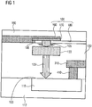
- Fig. 1 shows an example, which does not fall under the claims, in which a photodetector comprises a photodiode 115, which may be formed for example by a pn junction of an n-well to a substrate 117 or to a p + -doped surface layer (or a uses other existing pn junction).
- the photodiode 115 has a detector surface 120 and is contacted via the contact 410 with a shielding plane 310. Other contacts of the photodetector are again not shown for the sake of simplicity.
- the photodetector 115 and the OLED 100 are separated by a layer sequence 130 having a reservoir 133.
- the reservoir 133 may be formed as a reagent reservoir or microchannel and serve as a container for the medium to be examined (eg serum). It can thus simultaneously serve as a sample holder.
- the OLED 100 has a transparent electrode 180, an organic layer sequence 170 and a second electrode 160, wherein the transparent electrode 180 is deposited on the layer sequence 130. The chip is finally protected by a passivation 190. The side insulation 195 electrically isolates the transparent electrode 180 and the second electrode 160.
- a light signal 105 generated by the OLED 100 thus passes through the reservoir 133 and the light signal 105 'emanating from the reservoir 133 enters the photodetector 115 via the detector surface 120.
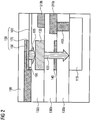
- Fig. 2 an embodiment is shown that differs from the one in Fig.
- ILD I nter L ayer D ielectricum
- IMD1 layer 130b I nter M etal D ielectricum
- IMD2 layer 130c IMD2 layer 130c.
- the IMD1 layer 130b For example, a shield plane 310a and the IMD2 layer 130c have a shield plane 310b.
- the photodetector 115 is connected to the shielding plane 310a via a bridge or via 410, which bridges the ILD layer 130a.
- the shield plane 310a thus serves to electrically connect the contact 410.
- the ILD layer 130a serves as protection for the photodiode 115 and the p-type substrate 117.
- the ILD layer 130a, the IMD1 layer 130b, and the IMD2 layer 130c are again typical components of a CMOS structure, as well as the shielding planes 310a and 310b, which may be implemented, for example, by metal line level of the CMOS structure.
- the second electrode 160 can be easily realized by CMOS metallization.
- the illustrated embodiment further includes an optional filter 140, which is formed here in the IMD1 layer 130b, wherein the filter 140 may be formed in other layers.
- the OLED as bottom emitter 100 generates from an electrical input signal the light signal 105, which passes through the IMD2 layer 130c and enters the reservoir 133.
- the light signal 105 'emanating from the reservoir 133 passes through the IMD1 layer 130b, the optional filter 140 and the ILD layer 130a before it enters the photodiode 115 and generates an electrical output signal there.
- the electrical output signal can measure the extinction, absorption, fluorescence, etc. of the light signal 105 'originating from the reservoir 133 as a measured variable.
- FIG. 12 shows an embodiment in which the OLED 100 indirectly radiates onto a photodetector 515 using a buried dielectric transparent layer 510 serving as a light guide.
- the dielectric transparent layer 510 (which may also be referred to as a buried layer) is deposited on a substrate 500 and serves as a base for the photodetector 515 and an OLED driver transistor 540.
- the photodetector 515 and the OLED driver transistor 540 are embedded in the ILD layer 130a and again the IMD1 layer 130b and the IMD2 layer 130c are deposited on the ILD layer 130a.
- the IMD2 layer also serves as a substrate for the subsequent OLED 100 with the transparent electrode 180, the organic layer sequence 170 and the second electrode 160, which in turn is embedded in a passivation 190, and the lateral insulation 195 provides insulation between the transparent electrode 180 and the second electrode 160.
- the photodetector 515 is electrically contacted via a first contact 520a and a second contact 520b.
- the first contact 520a is connected via a first bridge 410 1 to a first part 310a 1 of the shielding plane 310a.
- the second contact 520b is connected to a second part 310a 2 of the shielding plane 310a via a second bridge 410 2 , and the second part 310a 2 is in turn connected to the shielding plane 310b via a third bridge 530.
- Electrical contacting of the OLED driver transistor 540 takes place via a first part 310c 1 and via a second part 310c 2 of the shield plane 310c.
- the first part 310c 1 is connected via a fifth bridge 560 1 to a first part 310d 1 of the shielding plane 310d.
- the second part 310c 2 is a sixth bridge 560 2 connected to a second part 310d 2 of the shielding plane 310d.
- the second part 310d 2 is in turn via a seventh bridge 570 2 with the shielding plane 310e, which in turn is electrically connected via an eighth bridge 580 2 with the second electrode 160 of the OLED 100.
- the shielding planes 310b and 310e are embedded in the IMD2 layer 130c and the shielding planes 310a and 310d are embedded in the IMD1 layer 130b.
- the ILD layer 130a has the parts 310c 1 and 310c 2 of the shielding plane 310c as well as the contacts 520a and 520b.
- the structures called shielding planes are here can each be implemented by sections of metal line levels of a CMOS structure and serve via respective bridges or vias at least partially further than terminal structures.
- the light signal 105 emitted from the OLED 100 as a bottom emitter strikes the reservoir 133, and the light signal 105 'emanating from it passes through the optional filter 140 and strikes the incorporated dielectric transparent layer 510 serving as the optical waveguide serves.
- the light signal 105 ' thus generates in the dielectric, transparent layer 510 a light signal 590 which propagates in the direction of the photodetector 515 and generates there an electrical signal which is output via the contacts 520a and 520b.
- the first contact 520a is connected to the first part 310a 1 of the shielding plane 310a
- the second contact 520b is connected to the shielding plane 310b where the electrical signal is applied as the output signal.
- CMOS structure which are described, for example, in US Pat Fig. 3 are shown schematically.
- the embodiment of Fig. 3 is therefore based on a buried oxide layer SOI-CMOS technology that corresponds to the dielectric, transparent layer 510 and is simultaneously used as an electrical insulator and light guide.
- SOI-CMOS technology corresponds to the dielectric, transparent layer 510 and is simultaneously used as an electrical insulator and light guide.
- the photodetector 515 should be selected to be correspondingly large.
- An active layer which comprises, for example, silicon and is provided on the dielectric, transparent layer 510, should therefore be made sufficiently thick to form a high photon absorption probability.
- the reservoir 133 and the optional filter can be as in Fig. 1 and 2 be described described.
- structures denoted by the reference symbols 310d 1 , 310d 2 , 310a 1 and 310a 2 may each be parts of a first metal line level (MET1) of a CMOS structure, the structures 310b and 310e may be parts of a second metal line level (MET2), and the structure 160 may be part of a third metal line level (MET3).
- a complete evaluation and control unit is integrated.
- FIG. 12 shows an example which does not fall under the claims, in which an OLED 100 is used as a top emitter which irradiates indirectly on the photodetector 115.
- the photodetector 115 the photodiode (which is formed by an existing pn junction), which is contacted via the contact 410 and embedded in the p-type substrate 117.
- the contact 410 is connected to a metal line level 310 of the CMOS structure.
- the metal line level 310 is in the IMD1 layer 130b, which in turn connects to the ILD layer 130a.
- the OLED 100 is applied to the IMD1 layer 130b, wherein a metal line plane (MET2) formed on the IMD1 layer 130b serves as the lower electrode 160 to which the organic layer sequence 170 and the transparent electrode 180 are applied.
- a metal line plane (MET2) formed on the IMD1 layer 130b serves as the lower electrode 160 to which the organic layer sequence 170 and the transparent electrode 180 are applied.
- the passivation 190 follows, which has a transparent material.
- the side insulation 195 also provides insulation between the transparent electrode 180 and the second electrode 160.
- the contacting structures 310 and 160 may in turn be inherent parts of the CMOS structure, be configured as metal line levels and additionally serve as shielding levels.
- a reservoir is formed on the passivation 190 in this comparative example.
- the reservoir is arranged such that a light signal 105 from the OLED 100, which acts as a top emitter on the reservoir and the outgoing light signal 105 'is reflected onto the photodetector 115, ie, the light signal 105 is emitted in the direction of the reservoir and passes as a light signal 105 'in the photodiode 115, which is embedded in the p-substrate 117.
- the OLED 100 radiates upward, ie in the direction of the passivation 190 Fig. 4 can be seen in one embodiment to ensure that the photodetector 115 is not obscured by the shielding plane 310, so that the largest possible part of the output from the reservoir light signal 105 'reaches the photodetector 115.
- FIG. 12 shows a top view of one example of a possible sensor assembly 800 suitable for a lab-on-chip application, but not covered by the claims.
- a chip 810 there is a lattice-shaped OLED 100 and photodetectors (dashed areas) 115 in the respective spaces.
- photodetectors of different spectral sensitivity, it is possible to selectively detect a certain portion of the outgoing light signal 105 '(for example a component which fluoresces with a certain color) or to detect its movement or change.
- the reservoir may be formed in the form of various pots on a surface of the sensor assembly 800.
- the OLED 100 may be arranged as a top emitter.
- the reservoir it is likewise possible for the reservoir to be formed as a channel system (for example in an oxide layer), wherein the OLED 100 can then be embodied as a bottom emitter.
- the lattice-shaped OLED is constructed from a large number of bar or line-shaped OLEDs.
- a position of certain substances or objects on the chip can also be determined with this sensor arrangement.
- suitable OLEDs which excite certain substances or constituents of liquids, it is also possible with this sensor arrangement to determine concentrations of the specific substance as a function of the position on the chip. Also, detection of temporal changes (e.g., the concentration of a fluorescent substance) is possible.
- Fig. 6 shows a top view of a possible sensor arrangement 400, which does not fall under the claims, which is particularly suitable as a fluorescence sensor.
- the sensor arrangement 400 has, for example, two green OLEDs 410 1 and 410 2 as well as two blue OLEDs 420 1 and 420 2 , which are part of a circuit 430.
- two photodetectors 115 1 and 115 2 are arranged between the green OLEDs 410 1 and 410 2 and the blue OLEDs 420 1 and 420 2 , so that the green OLEDs 410 1 and 410 2 and the blue OLEDs 420 1 and 420 2 are ideally located at the same distance from the photodetectors 115 1 and 115 2 .
- further OLEDs and / or photodetectors may be provided.
- combinations with other colors or use of OLEDs of a different color are possible.
- the different OLEDs have the same distance as possible to the photodetectors 115 1 and 115 2 .
- fluorescence of substances can be excited and the corresponding fluorescence radiation, which is usually emitted to a different wavelength, can be detected and its temporal decay behavior (ie the weakening intensity) measured.
- the candidate substances can be detected by fluorescence.
- the photodetectors 115 1 and 115 2 have an increased sensitivity for the corresponding radiation caused by fluorescence.
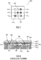
- Fig. 7 shows a top view of a sensor assembly 600, which does not fall under the claims, which is particularly suitable as a possible spectral / color sensor.
- This comparative example has four different OLEDs.
- a blue OLED 610, a green OLED 620, a red OLED 630 and a (near) infrared OLED 640 are together with photodetectors 115 1 , 115 2 , 115 3 ,...
- On a chip 650 which in this comparative example has a quadrangular shape has arranged.
- the photodetectors 115 1 , 115 2 , 115 3 , ... are arranged symmetrically on the chip 650, namely at each corner and in the middle there is a photodetector.
- the differently colored OLEDs are arranged along the four side lengths of the chip 650, with the blue OLED 610 on the left, the green OLED 620 on the bottom, the red OLED 630 on the right and the (near) infrared OLED 640 on the top being arranged in the plan view shown here.
- the choice of the arrangement of the OLEDs as well as the coloring is freely taken and the OLEDs can be exchanged accordingly in further comparative examples.
- the number of OLEDs and their color as well as the square shape of the chip 650 are exemplary only and may vary in further comparative examples.
- it is advantageous if the photodetectors 115 1 , 115 2 , 115 3 , ... are arranged as close as possible to the different OLEDs in order to obtain a similar spectral sensitivity (spectral range sensitivity) for all colors.
- mutual interference due to too short a distance should be excluded.
- This comparative example can be used as a color sensor, ie different reflection properties of colored objects or substances with regard to colored light can be detected selectively and thus objects or substances can be distinguished according to their color.
- OLEDs are available in many colors.
- the photodetectors 115 1 , 115 2 , 115 3 , ... are spectrally different in their sensitivity. This can be achieved, for example, by different implementations (such as the different diodes 975, 964 and 962 in FIG Fig. 8 ) happen.
- the different spectral sensitivities can be spectrally adjusted, for example, to the respective emitters.
- the OLEDs and the photodetectors are offset in height and the reservoir has been omitted for clarity.
- the photodetectors 115 based on a CMOS process may have different spectral characteristics. Further, it is possible to integrate organic light emitting diodes as a top emitter on a CMOS metal layer as a lower electrode.
- the photodetector 115 may be configured as any photosensitive device occurring in CMOS structures, and may include, for example, a photodiode or a phototransistor.
- the OLED In the lab-on-chip arrangement, the OLED often emits upward (top emitter), i. in the direction of the passivation and thus in the opposite direction to the photodetector 115.
- the sample, the medium or the reagent reflects the light, which may come to absorption, fluorescence or phosphorescence (static or time resolved), and directs the light 105 'on the Photodetector 115 back in the chip (in substrate).
- a control and evaluation electronics can be integrated into the CMOS chip (an example was in Fig. 3 shown). Such an arrangement in turn can be part of a complex be integrated circuit (IC), which may additionally have an optical coupler function as a microsystem.
- IC complex be integrated circuit
- the geometric arrangement of the light emitter 100 and the detector 115 can be adapted to the requirements of the measurement task.
- the advantage of the large-area deposition and structurability of OLED 100 comes into play.
- the area occupied by the OLED 100 in the ground can be used by an active circuit, which does not necessarily need to be linked to the OLED control.
- a focusing of the light signal 105 can take place via an optical system. This can be achieved, for example, by means of a lens or a mirror system and would be advantageous in that the detector surface 120 of the photodetector 115 can be selected correspondingly smaller and still obtain a sufficient amount of light.
- both analog and digitized signals can be used during operation.
- the photodetector 115 comprises an organic photovoltaic cell.
- a filter can be realized by using organic materials.
- Embodiments can thus be used for absorption spectroscopy, for example by illumination with a white OLED and filtering as described above.
- the white OLED or the white light which is emitted by the white OLED can be produced, for example, using stacked light-emitting diodes, when the light from the individual OLEDs is supplemented by superimposition to form white light.
- Embodiments also describe a use of OLED emitters with different wavelengths (different colors). It is also possible to use a pulsed OLED, for example, to measure a decay dynamics of the optical signals.
- photodiodes may be spatially arranged to measure OLED brightness, thereby allowing for homogeneity control.
- embodiments may be used as a spectral sensor or as a fluorescence sensor.
- CMOS circuit a CMOS circuit, bipolar IC technology, etc.
- MOS technology a MOS transistor
- bipolar IC technology a MOS transistor
- Comparative examples do not require the formation of a p-channel and n-channel transistor.
- OLED technology as an emitter offers the possibility of a monolithically integrated solution, which both reduces the size of the components and offers the possibility of integrating new functions.
- multichannel solutions can be integrated on a chip, whereby both the sample to be examined and its holder can likewise be realized on the chip (for example by means of a microchannel or microchannel system).
- embodiments also include a chip in which the further photodetectors are formed in a matrix arrangement, or in which the filter comprises an organic material, or in which the filter between the reservoir 133 and the photodetector 115 in the beam path of the light signal 105 can be introduced is.
- Embodiments further include a chip in which the organic light emitter 100 is formed, white light or in which the organic light emitter 100 is configured to emit pulsed light signals, or in which the further photodetectors are spatially arranged to measure a brightness of the organic light emitter 100 or in which the reservoir 133 is formed to form a serum or To use blood as a medium.
- embodiments also include a use of a chip as a lab-on-chip sensor, as a fluorescence sensor or as a spectral sensor.
Landscapes
- Physics & Mathematics (AREA)
- Spectroscopy & Molecular Physics (AREA)
- General Physics & Mathematics (AREA)
- Health & Medical Sciences (AREA)
- Biochemistry (AREA)
- Analytical Chemistry (AREA)
- Chemical & Material Sciences (AREA)
- General Health & Medical Sciences (AREA)
- Life Sciences & Earth Sciences (AREA)
- Immunology (AREA)
- Pathology (AREA)
- Nuclear Medicine, Radiotherapy & Molecular Imaging (AREA)
- Investigating, Analyzing Materials By Fluorescence Or Luminescence (AREA)
Claims (15)
- Puce destinée à l'analyse d'un milieu, aux caractéristiques suivantes:un émetteur de lumière organique (100) destiné à émettre un signal lumineux (105);un photodétecteur (115) présentant une surface de détection (120);une succession de couches (130) composée de couches diélectriques d'une structure CMOS dans lesquelles sont formés des étages conducteurs métalliques (310b) de la structure CMOS, qui sépare l'émetteur de lumière organique (100) et la surface de détection (120) et sert de substrat pour l'émetteur de lumière organique (100); etdans lequel l'émetteur de lumière organique (100) et le photodétecteur (115) peuvent être couplés optiquement par un trajet de faisceau du signal lumineux (105) et un réservoir (133) est disposé dans le trajet du faisceau du signal lumineux (105),caractérisé par le fait que l'émetteur de lumière organique (100) est réalisé sous forme d'émetteur de fond, pour émettre le signal lumineux (105) à travers la succession de couches (130) servant de substrat et que la puce présente le réservoir (133) dans lequel peut être introduit le support et qui est réalisé sous forme de canal dans la séquence de couches (130) composée de couches diélectriques (130a; 130b; 130c) de la structure CMOS.
- Puce selon la revendication 1 présentant d'autres émetteurs de lumière organiques et/ou d'autres photodétecteurs.
- Puce selon la revendication 2, dans laquelle les autres photodétecteurs présentent une sensibilité spectrale qui diffère de la sensibilité spectrale du photodétecteur (115).
- Puce selon l'une des revendications précédentes, dans laquelle le photodétecteur (115) présente une cellule photovoltaïque organique ou un semi-conducteur inorganique comme couche active.
- Puce selon l'une des revendications précédentes, présentant par ailleurs un filtre dans le trajet de faisceau du signal lumineux (105).
- Puce selon la revendication 5, dans laquelle l'émetteur de lumière organique (100) est conçu pour émettre le signal de lumière (105) dans une plage spectrale, et dans laquelle le filtre est réalisé pour filtrer la plage spectrale et laisser passer une plage spectrale à laquelle est sensible le photodétecteur (115).
- Puce selon l'une des revendications précédentes, dans laquelle l'émetteur de lumière organique (100) est conçu pour émettre le signal lumineux (105) dans une plage spectrale, et dans laquelle le photodétecteur (115) est sensible à la lumière incidente (105') dans une autre plage spectrale, la plage spectrale différant de l'autre plage spectrale.
- Puce selon l'une des revendications précédentes, dans laquelle l'émetteur de lumière organique (100) présente une pluralité de diodes électroluminescentes empilées, les diodes électroluminescentes empilées étant réalisées pour émettre de la lumière de sorte qu'une superposition de la lumière émise par les diodes électroluminescentes empilées résulte en une lumière blanche.
- Puce selon l'une des revendications précédentes, dans laquelle l'émetteur de lumière organique (100) est conçu pour émettre le signal lumineux (105) dans une plage spectrale, et présentant par ailleurs un autre émetteur de lumière organique, l'autre émetteur de lumière organique étant conçu pour émettre de la lumière dans une autre plage spectrale, la plage spectrale différant de l'autre plage spectrale.
- Puce selon l'une des revendications précédentes, dans laquelle l'émetteur de lumière organique (100) est conçu pour émettre des signaux lumineux pulsés.
- Puce selon l'une des revendications précédentes, présentant par ailleurs une unité d'évaluation et de commande (540), l'unité d'évaluation et de commande (540) étant intégrée sur un même substrat que le photodétecteur (115).
- Puce selon l'une des revendications précédentes, dans laquelle le réservoir présente des cavités qui représentent des micro-résonateurs, de sorte qu'un rayonnement partant du milieu puisse être influencé ou modifié par une onde se trouvant dans les micro-résonateurs.
- Puce selon l'une des revendications précédentes, présentant un autre réservoir et un autre photodétecteur, l'autre réservoir étant séparé spatialement du réservoir (133) et pouvant être couplé optiquement à l'autre photodétecteur, et l'autre photodétecteur présentant une sensibilité spectrale différant du photodétecteur (115).
- Utilisation d'une puce selon l'une des revendications précédentes comme capteur de laboratoire sur puce, capteur de fluorescence, ou comme capteur spectral.
- Procédé de fabrication d'une puce pour l'analyse d'un fluide, aux étapes suivantes consistant à:réaliser un photodétecteur (115) présentant une surface de détection (120);réaliser une succession de couches (130) composée de couches diélectriques (130a; 130b; 130c) d'une structure CMOS sur la surface de détection (120) du photodétecteur (115), dans la succession de couches étant formés des étages conducteurs métalliques (310b) de la structure CMOS;réaliser un émetteur de lumière organique (100) destiné à émettre un signal lumineux (105), la succession de couches (130) servant de substrat pour l'émetteur de lumière organique (100) et la succession de couches (130) étant disposée entre l'émetteur de lumière organique (100) et la surface de détection (120); etdans lequel l'émetteur de lumière organique (100) et le photodétecteur (115) sont réalisés de sorte qu'un trajet de faisceau du signal lumineux (105) couple optiquement l'émetteur de lumière organique (100) et le photodétecteur (115), etdans lequel un réservoir (133) est réalisé dans le trajet de faisceau du signal lumineux (105),caractérisé par le fait que l'émetteur de lumière organique (100) est réalisé sous forme d'un émetteur de fond pour émettre le signal lumineux (105) à travers la succession de couches (130) servant de substrat et que le réservoir (133) dans lequel peut être introduit le milieu est réalisé sous forme de canal dans la succession de couches (130) composée de couches diélectriques (130a; 130c; 130b) de la structure CMOS.
Applications Claiming Priority (1)
| Application Number | Priority Date | Filing Date | Title |
|---|---|---|---|
| DE102007056275A DE102007056275B3 (de) | 2007-11-22 | 2007-11-22 | Chip zum Analysieren eines Mediums mit integriertem organischem Lichtemitter |
Publications (2)
| Publication Number | Publication Date |
|---|---|
| EP2065698A1 EP2065698A1 (fr) | 2009-06-03 |
| EP2065698B1 true EP2065698B1 (fr) | 2017-07-19 |
Family
ID=40383840
Family Applications (1)
| Application Number | Title | Priority Date | Filing Date |
|---|---|---|---|
| EP08020309.4A Active EP2065698B1 (fr) | 2007-11-22 | 2008-11-21 | Puce destinée à l'analyse d'un milieu à l'aide d'un émetteur de lumière organique intégré et procédé pour fabriquer une telle puce |
Country Status (3)
| Country | Link |
|---|---|
| US (1) | US20090134309A1 (fr) |
| EP (1) | EP2065698B1 (fr) |
| DE (1) | DE102007056275B3 (fr) |
Families Citing this family (16)
| Publication number | Priority date | Publication date | Assignee | Title |
|---|---|---|---|---|
| DE102006040788B4 (de) * | 2006-08-31 | 2013-02-07 | Fraunhofer-Gesellschaft zur Förderung der angewandten Forschung e.V. | Integrierter Optokoppler mit organischem Lichtemitter und anorganischem Photodetektor |
| WO2010088761A1 (fr) * | 2009-02-06 | 2010-08-12 | Maziyar Khorasani | Procédé et appareil de manipulation et de détection d'analytes |
| EP2375242A1 (fr) * | 2010-04-06 | 2011-10-12 | FOM Institute for Atomic and Moleculair Physics | Dispositif intégré de détection de nanocavité plasmonique |
| GB201207918D0 (en) * | 2012-05-04 | 2012-06-20 | Univ Lincoln The | Detector apparatus and method |
| DE102012220045A1 (de) * | 2012-11-02 | 2014-05-08 | Osram Opto Semiconductors Gmbh | Verfahren zum Betrieb eines organischen optoelektronischen Bauelements |
| DE102012220050A1 (de) | 2012-11-02 | 2014-05-08 | Osram Opto Semiconductors Gmbh | Organisches optoelektronisches Bauelement und Verfahren zum Betrieb des organischen optoelektronischen Bauelements |
| DE102012220049A1 (de) * | 2012-11-02 | 2014-05-08 | Osram Opto Semiconductors Gmbh | Organisches optoelektronisches Bauelement und Verfahren zum Betrieb des organischen optoelektronischen Bauelements |
| DE102012220056A1 (de) | 2012-11-02 | 2014-02-13 | Osram Opto Semiconductors Gmbh | Organisches optoelektronisches bauelement und verfahren zum betrieb des organischen optoelektronischen bauelements |
| DE102012220020A1 (de) * | 2012-11-02 | 2014-05-08 | Osram Opto Semiconductors Gmbh | Organisches optoelektronisches bauelement und verfahren zum betrieb des organischen optoelektronischen bauelements |
| CN103022076B (zh) * | 2012-11-22 | 2015-12-23 | 深圳典邦科技有限公司 | 一种集成的微显示oled图像收发装置的制作方法 |
| DE102012222461A1 (de) | 2012-12-06 | 2014-06-12 | Osram Opto Semiconductors Gmbh | Organisches optoelektronisches Bauelement |
| GB2523135A (en) * | 2014-02-13 | 2015-08-19 | Molecular Vision Ltd | Assay device |
| GB2541421A (en) * | 2015-08-19 | 2017-02-22 | Molecular Vision Ltd | Assay device |
| US10115000B2 (en) | 2015-12-11 | 2018-10-30 | Synaptics Incorporated | Method and system for optical imaging using patterned illumination |
| CN106653934A (zh) * | 2016-10-20 | 2017-05-10 | 天津大学 | 一种基于标准cmos工艺的混合光互连系统 |
| DE102019117045B4 (de) | 2019-06-25 | 2021-01-07 | Sentronic GmbH - Gesellschaft für optische Meßsysteme | Sensormodul zur multiparametrischen Analyse eines Mediums |
Family Cites Families (8)
| Publication number | Priority date | Publication date | Assignee | Title |
|---|---|---|---|---|
| US6331438B1 (en) * | 1999-11-24 | 2001-12-18 | Iowa State University Research Foundation, Inc. | Optical sensors and multisensor arrays containing thin film electroluminescent devices |
| GB2369428B (en) * | 2000-11-22 | 2004-11-10 | Imperial College | Detection system |
| US20030035755A1 (en) * | 2001-08-16 | 2003-02-20 | Shu-Hui Chen | Organic electroluminescence (OEL)-based biochips |
| US7170605B2 (en) * | 2003-08-25 | 2007-01-30 | Evan Francis Cromwell | Active sensor and method for optical illumination and detection |
| US7768650B2 (en) * | 2004-04-21 | 2010-08-03 | Michael Bazylenko | Optoelectronic biochip |
| US20080213821A1 (en) * | 2004-05-06 | 2008-09-04 | Nanyang Technological University | Microfluidic Cell Sorter System |
| US7257279B2 (en) * | 2004-09-20 | 2007-08-14 | 3M Innovative Properties Company | Systems and methods for biosensing and microresonator sensors for same |
| US7280201B2 (en) * | 2004-12-17 | 2007-10-09 | Avago Technologies General Ip Pte Ltd | Sensor having integrated light detector and/or light source |
-
2007
- 2007-11-22 DE DE102007056275A patent/DE102007056275B3/de active Active
-
2008
- 2008-11-21 EP EP08020309.4A patent/EP2065698B1/fr active Active
- 2008-11-21 US US12/275,327 patent/US20090134309A1/en not_active Abandoned
Non-Patent Citations (2)
| Title |
|---|
| HU Y ET AL: "PHOTOTRANSISTOR PROPERTIES OF PENTACENE ORGANIC TRANSISTORS WITH POLY(METHLY METHACRYLATE) DIELECTRIC LAYER", JAPANESE JOURNAL OF APPLIED PHYSICS, JAPAN SOCIETY OF APPLIED PHYSICS, JP, vol. 45, no. 1, 1 January 2006 (2006-01-01), pages L96 - L98, XP001245483, ISSN: 0021-4922, DOI: 10.1143/JJAP.45.L96 * |
| Y H CHEN ET AL: "Analysis of DNA fragments by microchip electrophoresis fabricated on poly(methyl methacrylate) substrates using a wire-imprinting method", ELECTROPHORESIS, 1 January 2000 (2000-01-01), GERMANY, pages 165 - 170, XP055202392, Retrieved from the Internet <URL:http://www.ncbi.nlm.nih.gov/pubmed/10634483> [retrieved on 20150715], DOI: 10.1002/(SICI)1522-2683(20000101)21:1<165::AID-ELPS165>3.0.CO;2-I * |
Also Published As
| Publication number | Publication date |
|---|---|
| US20090134309A1 (en) | 2009-05-28 |
| EP2065698A1 (fr) | 2009-06-03 |
| DE102007056275B3 (de) | 2009-04-02 |
Similar Documents
| Publication | Publication Date | Title |
|---|---|---|
| EP2065698B1 (fr) | Puce destinée à l'analyse d'un milieu à l'aide d'un émetteur de lumière organique intégré et procédé pour fabriquer une telle puce | |
| DE102006040790B4 (de) | Reflexkoppler mit integriertem organischen Lichtemitter sowie Verwendung eines solchen Reflexkopplers | |
| EP0244394B1 (fr) | Elément de capteur pour la détermination de concentrations de substances | |
| EP1787108B1 (fr) | Dispositif d'analyse d'echantillons biochimiques | |
| DE10145701A1 (de) | Fluoreszenz-Biosensorchip und Fluoreszenz-Biosensorchip-Anordnung | |
| WO2004048881A2 (fr) | Dispositif de mesure pour l'examen optique d'un élément d'essai | |
| EP0918984B1 (fr) | Dispositif de detection optique | |
| EP0788615A1 (fr) | Procede et dispositif de determination de parametres, specifiques a une substance, d'une ou de plusieurs molecules par spectroscopie de correlation | |
| CN108139332A (zh) | 光学检测单元 | |
| DE10018550A1 (de) | Optoelektronischer Sensor | |
| WO2020156767A1 (fr) | Composant multi-spectral hybride | |
| DE19835769C2 (de) | Optoelektronischer Gassensor auf der Basis von Optoden | |
| WO2014086575A1 (fr) | Composant optoélectronique organique | |
| DE112018004522T5 (de) | Chemischer Sensor und Verfahren zum Bilden desselben | |
| DE102017110216B4 (de) | Optoelektronisches Sensormodul und Verfahren zur Herstellung eines optoelektronischen Sensormoduls | |
| WO2016012276A1 (fr) | Ensemble de détection avec résolution de position et de longueur d'onde d'un rayonnement lumineux qui est émis par au moins une oled ou une led | |
| EP1595137B1 (fr) | Procede et dispositifs permettant de determiner et surveiller des etats d'impuretes dans differents fluides | |
| DE112021006065T5 (de) | Teststreifenkassette, überwachungsvorrichtung und verfahren zur herstellung einer teststreifenkassette | |
| AT390330B (de) | Sensorelement zur bestimmung von stoffkonzentrationen | |
| WO2020160973A1 (fr) | Système de capteurs optoélectronique et procédé de mesure optique | |
| WO2004048170A1 (fr) | Procede pour determiner une vitesse de reference pour un vehicule | |
| DE102020210245B3 (de) | Gradiometer zur Erfassung eines Gradientenfeldes einer physikalischen Größe | |
| DE102022122954A1 (de) | Optoelektronisches Bauelement mit integrierter Aperturmaske | |
| DD292342A5 (de) | Biologische photozelle | |
| EP1887332A1 (fr) | Tête de mesure colorimétrique |
Legal Events
| Date | Code | Title | Description |
|---|---|---|---|
| PUAI | Public reference made under article 153(3) epc to a published international application that has entered the european phase |
Free format text: ORIGINAL CODE: 0009012 |
|
| AK | Designated contracting states |
Kind code of ref document: A1 Designated state(s): AT BE BG CH CY CZ DE DK EE ES FI FR GB GR HR HU IE IS IT LI LT LU LV MC MT NL NO PL PT RO SE SI SK TR |
|
| AX | Request for extension of the european patent |
Extension state: AL BA MK RS |
|
| 17P | Request for examination filed |
Effective date: 20091023 |
|
| AKX | Designation fees paid |
Designated state(s): AT BE BG CH CY CZ DE DK EE ES FI FR GB GR HR HU IE IS IT LI LT LU LV MC MT NL NO PL PT RO SE SI SK TR |
|
| 17Q | First examination report despatched |
Effective date: 20150720 |
|
| RIC1 | Information provided on ipc code assigned before grant |
Ipc: G01N 21/64 20060101AFI20161222BHEP Ipc: G01N 21/31 20060101ALI20161222BHEP Ipc: B01L 3/00 20060101ALN20161222BHEP |
|
| GRAP | Despatch of communication of intention to grant a patent |
Free format text: ORIGINAL CODE: EPIDOSNIGR1 |
|
| STAA | Information on the status of an ep patent application or granted ep patent |
Free format text: STATUS: GRANT OF PATENT IS INTENDED |
|
| INTG | Intention to grant announced |
Effective date: 20170202 |
|
| GRAS | Grant fee paid |
Free format text: ORIGINAL CODE: EPIDOSNIGR3 |
|
| GRAA | (expected) grant |
Free format text: ORIGINAL CODE: 0009210 |
|
| STAA | Information on the status of an ep patent application or granted ep patent |
Free format text: STATUS: THE PATENT HAS BEEN GRANTED |
|
| AK | Designated contracting states |
Kind code of ref document: B1 Designated state(s): AT BE BG CH CY CZ DE DK EE ES FI FR GB GR HR HU IE IS IT LI LT LU LV MC MT NL NO PL PT RO SE SI SK TR |
|
| REG | Reference to a national code |
Ref country code: GB Ref legal event code: FG4D Free format text: NOT ENGLISH |
|
| REG | Reference to a national code |
Ref country code: CH Ref legal event code: EP |
|
| REG | Reference to a national code |
Ref country code: IE Ref legal event code: FG4D Free format text: LANGUAGE OF EP DOCUMENT: GERMAN |
|
| REG | Reference to a national code |
Ref country code: AT Ref legal event code: REF Ref document number: 910855 Country of ref document: AT Kind code of ref document: T Effective date: 20170815 |
|
| REG | Reference to a national code |
Ref country code: DE Ref legal event code: R096 Ref document number: 502008015464 Country of ref document: DE |
|
| REG | Reference to a national code |
Ref country code: CH Ref legal event code: NV Representative=s name: BOVARD AG PATENT- UND MARKENANWAELTE, CH |
|
| REG | Reference to a national code |
Ref country code: NL Ref legal event code: MP Effective date: 20170719 |
|
| REG | Reference to a national code |
Ref country code: FR Ref legal event code: PLFP Year of fee payment: 10 |
|
| REG | Reference to a national code |
Ref country code: LT Ref legal event code: MG4D |
|
| PG25 | Lapsed in a contracting state [announced via postgrant information from national office to epo] |
Ref country code: FI Free format text: LAPSE BECAUSE OF FAILURE TO SUBMIT A TRANSLATION OF THE DESCRIPTION OR TO PAY THE FEE WITHIN THE PRESCRIBED TIME-LIMIT Effective date: 20170719 Ref country code: NL Free format text: LAPSE BECAUSE OF FAILURE TO SUBMIT A TRANSLATION OF THE DESCRIPTION OR TO PAY THE FEE WITHIN THE PRESCRIBED TIME-LIMIT Effective date: 20170719 Ref country code: HR Free format text: LAPSE BECAUSE OF FAILURE TO SUBMIT A TRANSLATION OF THE DESCRIPTION OR TO PAY THE FEE WITHIN THE PRESCRIBED TIME-LIMIT Effective date: 20170719 Ref country code: NO Free format text: LAPSE BECAUSE OF FAILURE TO SUBMIT A TRANSLATION OF THE DESCRIPTION OR TO PAY THE FEE WITHIN THE PRESCRIBED TIME-LIMIT Effective date: 20171019 Ref country code: SE Free format text: LAPSE BECAUSE OF FAILURE TO SUBMIT A TRANSLATION OF THE DESCRIPTION OR TO PAY THE FEE WITHIN THE PRESCRIBED TIME-LIMIT Effective date: 20170719 Ref country code: LT Free format text: LAPSE BECAUSE OF FAILURE TO SUBMIT A TRANSLATION OF THE DESCRIPTION OR TO PAY THE FEE WITHIN THE PRESCRIBED TIME-LIMIT Effective date: 20170719 |
|
| PG25 | Lapsed in a contracting state [announced via postgrant information from national office to epo] |
Ref country code: IS Free format text: LAPSE BECAUSE OF FAILURE TO SUBMIT A TRANSLATION OF THE DESCRIPTION OR TO PAY THE FEE WITHIN THE PRESCRIBED TIME-LIMIT Effective date: 20171119 Ref country code: ES Free format text: LAPSE BECAUSE OF FAILURE TO SUBMIT A TRANSLATION OF THE DESCRIPTION OR TO PAY THE FEE WITHIN THE PRESCRIBED TIME-LIMIT Effective date: 20170719 Ref country code: GR Free format text: LAPSE BECAUSE OF FAILURE TO SUBMIT A TRANSLATION OF THE DESCRIPTION OR TO PAY THE FEE WITHIN THE PRESCRIBED TIME-LIMIT Effective date: 20171020 Ref country code: LV Free format text: LAPSE BECAUSE OF FAILURE TO SUBMIT A TRANSLATION OF THE DESCRIPTION OR TO PAY THE FEE WITHIN THE PRESCRIBED TIME-LIMIT Effective date: 20170719 Ref country code: PL Free format text: LAPSE BECAUSE OF FAILURE TO SUBMIT A TRANSLATION OF THE DESCRIPTION OR TO PAY THE FEE WITHIN THE PRESCRIBED TIME-LIMIT Effective date: 20170719 Ref country code: BG Free format text: LAPSE BECAUSE OF FAILURE TO SUBMIT A TRANSLATION OF THE DESCRIPTION OR TO PAY THE FEE WITHIN THE PRESCRIBED TIME-LIMIT Effective date: 20171019 |
|
| REG | Reference to a national code |
Ref country code: DE Ref legal event code: R097 Ref document number: 502008015464 Country of ref document: DE |
|
| PG25 | Lapsed in a contracting state [announced via postgrant information from national office to epo] |
Ref country code: RO Free format text: LAPSE BECAUSE OF FAILURE TO SUBMIT A TRANSLATION OF THE DESCRIPTION OR TO PAY THE FEE WITHIN THE PRESCRIBED TIME-LIMIT Effective date: 20170719 Ref country code: DK Free format text: LAPSE BECAUSE OF FAILURE TO SUBMIT A TRANSLATION OF THE DESCRIPTION OR TO PAY THE FEE WITHIN THE PRESCRIBED TIME-LIMIT Effective date: 20170719 Ref country code: CZ Free format text: LAPSE BECAUSE OF FAILURE TO SUBMIT A TRANSLATION OF THE DESCRIPTION OR TO PAY THE FEE WITHIN THE PRESCRIBED TIME-LIMIT Effective date: 20170719 |
|
| PLBE | No opposition filed within time limit |
Free format text: ORIGINAL CODE: 0009261 |
|
| STAA | Information on the status of an ep patent application or granted ep patent |
Free format text: STATUS: NO OPPOSITION FILED WITHIN TIME LIMIT |
|
| PG25 | Lapsed in a contracting state [announced via postgrant information from national office to epo] |
Ref country code: SK Free format text: LAPSE BECAUSE OF FAILURE TO SUBMIT A TRANSLATION OF THE DESCRIPTION OR TO PAY THE FEE WITHIN THE PRESCRIBED TIME-LIMIT Effective date: 20170719 Ref country code: EE Free format text: LAPSE BECAUSE OF FAILURE TO SUBMIT A TRANSLATION OF THE DESCRIPTION OR TO PAY THE FEE WITHIN THE PRESCRIBED TIME-LIMIT Effective date: 20170719 Ref country code: IT Free format text: LAPSE BECAUSE OF FAILURE TO SUBMIT A TRANSLATION OF THE DESCRIPTION OR TO PAY THE FEE WITHIN THE PRESCRIBED TIME-LIMIT Effective date: 20170719 |
|
| 26N | No opposition filed |
Effective date: 20180420 |
|
| PG25 | Lapsed in a contracting state [announced via postgrant information from national office to epo] |
Ref country code: MC Free format text: LAPSE BECAUSE OF FAILURE TO SUBMIT A TRANSLATION OF THE DESCRIPTION OR TO PAY THE FEE WITHIN THE PRESCRIBED TIME-LIMIT Effective date: 20170719 |
|
| PG25 | Lapsed in a contracting state [announced via postgrant information from national office to epo] |
Ref country code: SI Free format text: LAPSE BECAUSE OF FAILURE TO SUBMIT A TRANSLATION OF THE DESCRIPTION OR TO PAY THE FEE WITHIN THE PRESCRIBED TIME-LIMIT Effective date: 20170719 Ref country code: LU Free format text: LAPSE BECAUSE OF NON-PAYMENT OF DUE FEES Effective date: 20171121 |
|
| REG | Reference to a national code |
Ref country code: BE Ref legal event code: MM Effective date: 20171130 |
|
| REG | Reference to a national code |
Ref country code: IE Ref legal event code: MM4A |
|
| PG25 | Lapsed in a contracting state [announced via postgrant information from national office to epo] |
Ref country code: MT Free format text: LAPSE BECAUSE OF FAILURE TO SUBMIT A TRANSLATION OF THE DESCRIPTION OR TO PAY THE FEE WITHIN THE PRESCRIBED TIME-LIMIT Effective date: 20170719 |
|
| PG25 | Lapsed in a contracting state [announced via postgrant information from national office to epo] |
Ref country code: IE Free format text: LAPSE BECAUSE OF NON-PAYMENT OF DUE FEES Effective date: 20171121 |
|
| PG25 | Lapsed in a contracting state [announced via postgrant information from national office to epo] |
Ref country code: BE Free format text: LAPSE BECAUSE OF NON-PAYMENT OF DUE FEES Effective date: 20171130 |
|
| REG | Reference to a national code |
Ref country code: AT Ref legal event code: MM01 Ref document number: 910855 Country of ref document: AT Kind code of ref document: T Effective date: 20171121 |
|
| PG25 | Lapsed in a contracting state [announced via postgrant information from national office to epo] |
Ref country code: AT Free format text: LAPSE BECAUSE OF NON-PAYMENT OF DUE FEES Effective date: 20171121 |
|
| PG25 | Lapsed in a contracting state [announced via postgrant information from national office to epo] |
Ref country code: HU Free format text: LAPSE BECAUSE OF FAILURE TO SUBMIT A TRANSLATION OF THE DESCRIPTION OR TO PAY THE FEE WITHIN THE PRESCRIBED TIME-LIMIT; INVALID AB INITIO Effective date: 20081121 |
|
| PG25 | Lapsed in a contracting state [announced via postgrant information from national office to epo] |
Ref country code: CY Free format text: LAPSE BECAUSE OF NON-PAYMENT OF DUE FEES Effective date: 20170719 |
|
| PG25 | Lapsed in a contracting state [announced via postgrant information from national office to epo] |
Ref country code: TR Free format text: LAPSE BECAUSE OF FAILURE TO SUBMIT A TRANSLATION OF THE DESCRIPTION OR TO PAY THE FEE WITHIN THE PRESCRIBED TIME-LIMIT Effective date: 20170719 |
|
| PG25 | Lapsed in a contracting state [announced via postgrant information from national office to epo] |
Ref country code: PT Free format text: LAPSE BECAUSE OF FAILURE TO SUBMIT A TRANSLATION OF THE DESCRIPTION OR TO PAY THE FEE WITHIN THE PRESCRIBED TIME-LIMIT Effective date: 20170719 |
|
| PGFP | Annual fee paid to national office [announced via postgrant information from national office to epo] |
Ref country code: CH Payment date: 20211123 Year of fee payment: 14 |
|
| P01 | Opt-out of the competence of the unified patent court (upc) registered |
Effective date: 20230524 |
|
| REG | Reference to a national code |
Ref country code: CH Ref legal event code: PL |
|
| PG25 | Lapsed in a contracting state [announced via postgrant information from national office to epo] |
Ref country code: LI Free format text: LAPSE BECAUSE OF NON-PAYMENT OF DUE FEES Effective date: 20221130 Ref country code: CH Free format text: LAPSE BECAUSE OF NON-PAYMENT OF DUE FEES Effective date: 20221130 |
|
| PGFP | Annual fee paid to national office [announced via postgrant information from national office to epo] |
Ref country code: GB Payment date: 20231123 Year of fee payment: 16 |
|
| PGFP | Annual fee paid to national office [announced via postgrant information from national office to epo] |
Ref country code: FR Payment date: 20231122 Year of fee payment: 16 Ref country code: DE Payment date: 20231120 Year of fee payment: 16 |