EP2065489A1 - PROCESS FOR PRODUCING GaN SINGLE-CRYSTAL, GaN THIN-FILM TEMPLATE SUBSTRATE AND GaN SINGLE-CRYSTAL GROWING APPARATUS - Google Patents
PROCESS FOR PRODUCING GaN SINGLE-CRYSTAL, GaN THIN-FILM TEMPLATE SUBSTRATE AND GaN SINGLE-CRYSTAL GROWING APPARATUS Download PDFInfo
- Publication number
- EP2065489A1 EP2065489A1 EP07807346A EP07807346A EP2065489A1 EP 2065489 A1 EP2065489 A1 EP 2065489A1 EP 07807346 A EP07807346 A EP 07807346A EP 07807346 A EP07807346 A EP 07807346A EP 2065489 A1 EP2065489 A1 EP 2065489A1
- Authority
- EP
- European Patent Office
- Prior art keywords
- substrate
- gas
- gan
- single crystal
- gan single
- Prior art date
- Legal status (The legal status is an assumption and is not a legal conclusion. Google has not performed a legal analysis and makes no representation as to the accuracy of the status listed.)
- Withdrawn
Links
Images
Classifications
-
- C—CHEMISTRY; METALLURGY
- C30—CRYSTAL GROWTH
- C30B—SINGLE-CRYSTAL GROWTH; UNIDIRECTIONAL SOLIDIFICATION OF EUTECTIC MATERIAL OR UNIDIRECTIONAL DEMIXING OF EUTECTOID MATERIAL; REFINING BY ZONE-MELTING OF MATERIAL; PRODUCTION OF A HOMOGENEOUS POLYCRYSTALLINE MATERIAL WITH DEFINED STRUCTURE; SINGLE CRYSTALS OR HOMOGENEOUS POLYCRYSTALLINE MATERIAL WITH DEFINED STRUCTURE; AFTER-TREATMENT OF SINGLE CRYSTALS OR A HOMOGENEOUS POLYCRYSTALLINE MATERIAL WITH DEFINED STRUCTURE; APPARATUS THEREFOR
- C30B25/00—Single-crystal growth by chemical reaction of reactive gases, e.g. chemical vapour-deposition growth
- C30B25/02—Epitaxial-layer growth
- C30B25/14—Feed and outlet means for the gases; Modifying the flow of the reactive gases
-
- C—CHEMISTRY; METALLURGY
- C23—COATING METALLIC MATERIAL; COATING MATERIAL WITH METALLIC MATERIAL; CHEMICAL SURFACE TREATMENT; DIFFUSION TREATMENT OF METALLIC MATERIAL; COATING BY VACUUM EVAPORATION, BY SPUTTERING, BY ION IMPLANTATION OR BY CHEMICAL VAPOUR DEPOSITION, IN GENERAL; INHIBITING CORROSION OF METALLIC MATERIAL OR INCRUSTATION IN GENERAL
- C23C—COATING METALLIC MATERIAL; COATING MATERIAL WITH METALLIC MATERIAL; SURFACE TREATMENT OF METALLIC MATERIAL BY DIFFUSION INTO THE SURFACE, BY CHEMICAL CONVERSION OR SUBSTITUTION; COATING BY VACUUM EVAPORATION, BY SPUTTERING, BY ION IMPLANTATION OR BY CHEMICAL VAPOUR DEPOSITION, IN GENERAL
- C23C16/00—Chemical coating by decomposition of gaseous compounds, without leaving reaction products of surface material in the coating, i.e. chemical vapour deposition [CVD] processes
- C23C16/22—Chemical coating by decomposition of gaseous compounds, without leaving reaction products of surface material in the coating, i.e. chemical vapour deposition [CVD] processes characterised by the deposition of inorganic material, other than metallic material
- C23C16/30—Deposition of compounds, mixtures or solid solutions, e.g. borides, carbides, nitrides
- C23C16/34—Nitrides
-
- C—CHEMISTRY; METALLURGY
- C30—CRYSTAL GROWTH
- C30B—SINGLE-CRYSTAL GROWTH; UNIDIRECTIONAL SOLIDIFICATION OF EUTECTIC MATERIAL OR UNIDIRECTIONAL DEMIXING OF EUTECTOID MATERIAL; REFINING BY ZONE-MELTING OF MATERIAL; PRODUCTION OF A HOMOGENEOUS POLYCRYSTALLINE MATERIAL WITH DEFINED STRUCTURE; SINGLE CRYSTALS OR HOMOGENEOUS POLYCRYSTALLINE MATERIAL WITH DEFINED STRUCTURE; AFTER-TREATMENT OF SINGLE CRYSTALS OR A HOMOGENEOUS POLYCRYSTALLINE MATERIAL WITH DEFINED STRUCTURE; APPARATUS THEREFOR
- C30B25/00—Single-crystal growth by chemical reaction of reactive gases, e.g. chemical vapour-deposition growth
- C30B25/02—Epitaxial-layer growth
- C30B25/18—Epitaxial-layer growth characterised by the substrate
- C30B25/20—Epitaxial-layer growth characterised by the substrate the substrate being of the same materials as the epitaxial layer
-
- C—CHEMISTRY; METALLURGY
- C30—CRYSTAL GROWTH
- C30B—SINGLE-CRYSTAL GROWTH; UNIDIRECTIONAL SOLIDIFICATION OF EUTECTIC MATERIAL OR UNIDIRECTIONAL DEMIXING OF EUTECTOID MATERIAL; REFINING BY ZONE-MELTING OF MATERIAL; PRODUCTION OF A HOMOGENEOUS POLYCRYSTALLINE MATERIAL WITH DEFINED STRUCTURE; SINGLE CRYSTALS OR HOMOGENEOUS POLYCRYSTALLINE MATERIAL WITH DEFINED STRUCTURE; AFTER-TREATMENT OF SINGLE CRYSTALS OR A HOMOGENEOUS POLYCRYSTALLINE MATERIAL WITH DEFINED STRUCTURE; APPARATUS THEREFOR
- C30B29/00—Single crystals or homogeneous polycrystalline material with defined structure characterised by the material or by their shape
- C30B29/10—Inorganic compounds or compositions
- C30B29/38—Nitrides
-
- C—CHEMISTRY; METALLURGY
- C30—CRYSTAL GROWTH
- C30B—SINGLE-CRYSTAL GROWTH; UNIDIRECTIONAL SOLIDIFICATION OF EUTECTIC MATERIAL OR UNIDIRECTIONAL DEMIXING OF EUTECTOID MATERIAL; REFINING BY ZONE-MELTING OF MATERIAL; PRODUCTION OF A HOMOGENEOUS POLYCRYSTALLINE MATERIAL WITH DEFINED STRUCTURE; SINGLE CRYSTALS OR HOMOGENEOUS POLYCRYSTALLINE MATERIAL WITH DEFINED STRUCTURE; AFTER-TREATMENT OF SINGLE CRYSTALS OR A HOMOGENEOUS POLYCRYSTALLINE MATERIAL WITH DEFINED STRUCTURE; APPARATUS THEREFOR
- C30B29/00—Single crystals or homogeneous polycrystalline material with defined structure characterised by the material or by their shape
- C30B29/10—Inorganic compounds or compositions
- C30B29/40—AIIIBV compounds wherein A is B, Al, Ga, In or Tl and B is N, P, As, Sb or Bi
- C30B29/403—AIII-nitrides
- C30B29/406—Gallium nitride
-
- H—ELECTRICITY
- H10—SEMICONDUCTOR DEVICES; ELECTRIC SOLID-STATE DEVICES NOT OTHERWISE PROVIDED FOR
- H10P—GENERIC PROCESSES OR APPARATUS FOR THE MANUFACTURE OR TREATMENT OF DEVICES COVERED BY CLASS H10
- H10P14/00—Formation of materials, e.g. in the shape of layers or pillars
- H10P14/20—Formation of materials, e.g. in the shape of layers or pillars of semiconductor materials
-
- H—ELECTRICITY
- H10—SEMICONDUCTOR DEVICES; ELECTRIC SOLID-STATE DEVICES NOT OTHERWISE PROVIDED FOR
- H10P—GENERIC PROCESSES OR APPARATUS FOR THE MANUFACTURE OR TREATMENT OF DEVICES COVERED BY CLASS H10
- H10P14/00—Formation of materials, e.g. in the shape of layers or pillars
- H10P14/20—Formation of materials, e.g. in the shape of layers or pillars of semiconductor materials
- H10P14/24—Formation of materials, e.g. in the shape of layers or pillars of semiconductor materials using chemical vapour deposition [CVD]
-
- H—ELECTRICITY
- H10—SEMICONDUCTOR DEVICES; ELECTRIC SOLID-STATE DEVICES NOT OTHERWISE PROVIDED FOR
- H10P—GENERIC PROCESSES OR APPARATUS FOR THE MANUFACTURE OR TREATMENT OF DEVICES COVERED BY CLASS H10
- H10P14/00—Formation of materials, e.g. in the shape of layers or pillars
- H10P14/20—Formation of materials, e.g. in the shape of layers or pillars of semiconductor materials
- H10P14/29—Formation of materials, e.g. in the shape of layers or pillars of semiconductor materials characterised by the substrates
- H10P14/2901—Materials
- H10P14/2921—Materials being crystalline insulating materials
-
- H—ELECTRICITY
- H10—SEMICONDUCTOR DEVICES; ELECTRIC SOLID-STATE DEVICES NOT OTHERWISE PROVIDED FOR
- H10P—GENERIC PROCESSES OR APPARATUS FOR THE MANUFACTURE OR TREATMENT OF DEVICES COVERED BY CLASS H10
- H10P14/00—Formation of materials, e.g. in the shape of layers or pillars
- H10P14/20—Formation of materials, e.g. in the shape of layers or pillars of semiconductor materials
- H10P14/34—Deposited materials, e.g. layers
- H10P14/3402—Deposited materials, e.g. layers characterised by the chemical composition
- H10P14/3414—Deposited materials, e.g. layers characterised by the chemical composition being group IIIA-VIA materials
- H10P14/3416—Nitrides
Definitions
- the present invention relates to a manufacturing method of a GaN single crystal, which is applied with a hydride vapor phase epitaxy, and also related to a GaN single crystal growing apparatus, and a GaN thin film template substrate which is applied to manufacturing a light-emitting device such as a blue LED, and the like.
- a hydride vapor phase epitaxy in which by using a metallic chloride which is generated by a reaction of a heated metallic source material with a hydrogen chloride as source material gas, a crystal is grown from the chloride gas and hydroxide gas of a nonmetallic material.
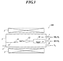
- FIG. 3 is a schematic configuration diagram showing the structure of a conventional vapor phase growing apparatus (an HVPE apparatus).
- An HVPE apparatus 100 is configured with a reacting furnace 1 which is sealed, and resistance heaters 2 which are provided at an outer circumference of the reacting furnace 1.
- the reacting furnace 1 is provided with an HCl gas supplying pipe 6 to supply HCl gas to generate a group III source material gas; a group V source material gas supplying pipe 7 to supply group V source material gas such as NH 3 gas, and the like, into the reacting furnace; an N 2 gas supplying pipe 8 to supply N 2 gas into the reacting furnace; a gas discharging pipe 3; and a substrate holder 4 to place a substrate 11.
- a source material placing section 10 is provided in the HCl gas supplying pipe 6, and a metallic source material 9 is disposed at this section to generate the group III source material gas. Moreover, the group III source material gas which is generated by the reaction of the HCl gas with the metallic source material 9 is sprayed onto the substrate 11 through a supplying nozzle 12.
- a cold-wall heating method is applied, in which only the circumference of the substrate is directly heated, and the wall temperature of the reacting furnace does not rise.
- a hot-wall heating method is applied in the HVPE apparatus 100, in which the entire reacting furnace is heated. That is to say, the HVPE method is designed to heat an area from a source material section in which the metallic source material is provided, through a mixing section in which the source material gas is mixed, to a growing section in which the reaction is proceeded so as to grow the crystal.
- the HVPE method has an advantage in that the crystal can be grown in a relatively high speed by supplying the source material gas on a massive scale.
- a gallium chloride (GaCl) which is generated by the reaction of a metallic gallium (Ga) with a hydrogen chloride (HCl) is used as the group III source material, and an ammonia (NH 3 ) is used as the group V source material.
- the thermal decomposition rate of the ammonia is said to be a few %, which is lower compared to that of an arsine (AsH 3 ) which is used as the group V source material when a crystal of a gallium arsenide (GaAs) is grown, and to that of a phosphine (PH 3 ) which is used as the group V source material when a crystal of an indium phosphide (InP) is grown. Accordingly, it is inevitably necessary to enlarge the proportion of V/III which is the supplying proportion of group V source material to the group III source material, when the crystal of GaN single crystal is grown.
- the following reaction pipe configuration is employed, as shown in FIG. 3 . That is, a massive NH 3 is gradually supplied from the group V source material gas supplying pipe 7, so as to be a laminar flow in the entire reacting furnace, and a small amount of GaCl which is generated by the reaction of the HCl with metallic Ga 9, is sprayed onto the substrate 11 in the growing section by the nozzle 12.
- Patent Documents 1-5 disclose that a rare earth group 3B perovskite substrate, especially an NGO substrate, is useful for the substrate for growing a GaN system compound semiconductor single crystal.
- the HVPE method has been considered to be unsuitable for manufacturing a GaN thin film template substrate in which an uniformity of film thickness and a high quality of the crystal are required. Accordingly, the GaN thin film template substrate which is currently offered commercially is manufactured mainly by the MBE method or by the MOVPE method.
- the GaN thin film template substrate is manufactured by the above mentioned MBE method or the MOCVD method, a sapphire or the like, in which the lattice constant thereof greatly differs from that of GaN is used as the substrate crystal.
- a GaN polycrystal which is referred to as a low temperature buffer layer is grown by approximately 100 nm at 500-600°C on the sapphire substrate, and subsequently, a GaN single crystal is grown by a few micrometers at approximately 1000°C as a template layer, thus the GaN thin film template substrate is manufactured.
- the above mentioned low temperature buffer layer cannot be subjected to XRD measurement in many cases due to being a polycrystal. Further, even when the low temperature buffer layer can be evaluated, a full width at half maximum thereof is tens of thousands of seconds (Non-Patent Document 1).
- the object of the present invention is to provide a manufacturing method of GaN single crystal, in which the film thickness and the composition of the GaN single crystal can be accurately controlled even when the hydride vapor phase epitaxiy is applied, and to provide a GaN thin film template substrate which is suitable for growing a GaN thick film with fine property, and a GaN single crystal growing apparatus.
- the present invention is made in order to solve the above mentioned object, and provided is a manufacturing method of a GaN single crystal by a hydride vapor phase epitaxy, wherein the hydride vapor phase epitaxy comprises: spraying HCl (hydrogen chloride) onto Ga (gallium) which is heated and fused in a predetermined temperature to generate GaCl (gallium chloride); and forming a GaN thin film by a reaction of the generated GaCl (gallium chloride) with NH 3 (ammonia) which is hydroxide gas on a substrate, the manufacturing method comprising supplying the NH 3 gas in a vicinity of the substrate through a nozzle.
- the nozzle means a member to squirt fluid at a high speed, and the shape thereof is not particularly limited. Generally, a cylindrical one with a thinned end, or the like, is applied.
- the starting and stopping of the NH 3 supply can be performed instantly, and the NH 3 remaining in the reacting furnace after the NH 3 supply is stopped is to be reduced.
- the NH 3 gas is supplied at a position which is separated from the substrate by a distance of 0.7-4.0 times as longer than a diameter of the substrate. That is to say, the nozzle to supply the NH 3 gas is disposed so that the substrate and the nozzle end are separated from each other by the distance of 0.7-4.0 times as longer than the diameter of the substrate.
- an NGO(011) substrate in which the lattice constant thereof is similar to that of GaN is used.
- a GaN single crystal with high quality in which for example, the full width at half maximum by the XRD measurement is not more than 1000 seconds, more preferably, the full width at half maximum is not more than 500 seconds, and even more preferably, the full width at half maximum is not more than 200 seconds, can be grown.
- the GaN single crystal growing apparatus (100) comprises: a reacting furnace (1) which is sealed; a resistance heater (2) which is provided at an outer circumference of the reacting furnace; a GaCl gas supplying section (7, 10) to supply GaCl gas as group III source material gas from a supply port into the reacting furnace; an NH 3 gas supplying section (5, 6) to supply NH 3 gas as group V source material gas from a supplying nozzle into the reacting furnace; an N 2 gas supplying section (8) to supply N 2 gas into the reacting furnace; a gas discharging section (3); and a substrate holder (4) to place a substrate, wherein an end of the supplying nozzle is located closer to the substrate than the supply port of the group III source material gas supplying section.
- the GaN single crystal is grown on the NGO(011) substrate, and subsequently, the supply of the source material gas is stopped instantly, thus superfluous NH 3 can be prevented from remaining in the reacting furnace.
- the growth of the GaN single crystal can reliably be prevented from proceeding, and the film thickness of the GaN single crystal can be controlled extremely accurately (for example, in a nanometer order) even when the HVPE method is applied.
- the HVPE method is applied, the GaN single crystal can be grown in a relatively high speed, and the manufacturing cost of the GaN single crystal can be reduced.
- the full width at half maximum by the XRD measurement is to be not more than 1000 seconds, thus the GaN thin film template can stably exist even when heated to approximately 1000°C which is a general growing temperature of the GaN single crystal.
- a GaN thick film with high quality can be formed by using the GaN thin film template, thus can realize a light-emitting device such as a blue LED, and the like, with excellent property.
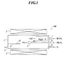
- FIG. 1 is a schematic configuration diagram showing the structure of a vapor phase growing apparatus (an HVPE apparatus) according to the embodiment.
- the HVPE apparatus 100 is configured with a reacting furnace 1 which is sealed, and resistance heaters 2 which are provided at an outer circumference of the reacting furnace 1.
- the reacting furnace 1 is provided with an HCl gas supplying pipe 7 to supply HCl gas to generate a group III source material gas; a group V source material gas supplying pipe 6 to supply group V source material gas such as NH 3 gas, and the like, into the reacting furnace; an N 2 gas supplying pipe 8 to supply N 2 gas into the reacting furnace; a gas discharging pipe 3; and a substrate holder 4 to place a substrate 11.
- HCl gas supplying pipe 7 to supply HCl gas to generate a group III source material gas
- a group V source material gas supplying pipe 6 to supply group V source material gas such as NH 3 gas, and the like, into the reacting furnace
- an N 2 gas supplying pipe 8 to supply N 2 gas into the reacting furnace
- a gas discharging pipe 3 to place a substrate 11.
- a source material placing section 10 is provided in the HCl gas supplying pipe 6, and a metallic source material 9 is disposed at this section to generate the group III source material gas. Moreover, in the present embodiment, a supplying nozzle 5 is provided at the end of the group V source material gas supplying pipe 6, so that the NH 3 gas is sprayed onto the substrate 11 through the supplying nozzle 5.
- the supplying nozzle 5 is provided so that the end thereof is closer to the substrate than the supply port provided at the source material placing section 10.
- the supplying nozzle 5 is provided so that the substrate and the end of the supplying nozzle 5 are separated from each other by the distance of 0.7-4.0 times as longer than the diameter of the substrate.
- the present embodiment an NGO(011) in which the lattice constant thereof is similar to that of GaN is used as the substrate for crystal growth.
- the group III source material gas is GaCl which is generated from metallic Ga and HCl
- the group V source material gas is NH 3 .
- the distance between the supplying nozzle 5 and the substrate 11 is 100 mm (which is 1.97 times as longer than the diameter of the substrate).
- an ingot of the NGO(011) is sliced so as to make the substrate for the crystal growth. On this occasion, the diameter of the NGO substrate is 2 inches, and the thickness thereof is 350 ⁇ m.
- the substrate temperature is increased to 600°C in a state where N 2 gas is introduced thereto through the N 2 gas supplying pipe 8.
- HCl gas is introduced through the HCl gas supplying pipe 6, and GaCl is generated by the reaction of metallic Ga 9 with HCl, so as to supply the generated GaCl onto the NGO substrate 11.
- NH 3 gas is supplied onto the NGO substrate 11 from the NH 3 gas supplying pipe 7 through the supplying nozzle 5.
- N 2 gas is applied as the carrier gas.
- the GaN compound semiconductor crystal is grown in a growth rate of approximately 0.72 ⁇ m/h in a state of controlling the gas introduction amount so that the partial pressure of GaCl be 0.002 atm, and the partial pressure of NH 3 be 0.066 atm, respectively.
- the group V source material gas (NH 3 ) is supplied in the vicinity of the NGO(011) substrate 11 through the nozzle, thus the supply of the source material gas can instantly be stopped after the growth of the GaN single crystal is terminated.
- the NH 3 can be prevented from remaining in the reacting furnace after the supply of the source material gas is stopped, and reaction does not happen even when GaCl flows out from the surface of the Ga source material.
- the growth of the GaN single crystal can reliably be prevented from proceeding after the supply of the source material gas is stopped.
- Tables 1 and 2 show the measurement results of film thickness and full width at half maximum by XRD (X-ray diffraction) at 5 points in the wafer surface of the GaN single crystal thin film which is obtained by the above described manufacturing method.
- table 1 is a measurement result pertaining to GaN single crystal A which is grown in a state where the film thickness is controlled to be 60 nm
- table 2 is a measurement result pertaining to GaN single crystal B which is grown in a state where the film thickness is controlled to be 65 nm.
- the difference between the maximum film thickness and the minimum film thickness is 4.298 nm, and error from the controlled film thickness is 1.677-2.621 nm.
- the difference between the maximum film thickness and the minimum film thickness is 3.340 nm, and error from the controlled film thickness is 2.365-0.975 nm. From these results, it can be confirmed that the film thickness of GaN single crystal can be controlled accurately and uniformly in the manufacturing method applying the HVPE method.
- the full width at half maximum by the XRD of either of GaN single crystals A and B is not more than 200 seconds.
- the NGO(011) substrate in which the lattice constant thereof is similar to that of GaN is used, a GaN single crystal with high quality can be grown. Further, the GaN single crystal is grown on the NGO substrate, and after the supply of the source material gas is stopped, the NH 3 can be prevented from remaining in the reacting furnace. Thus, even when GaCl flows out from the surface of the Ga source material, reaction does not happen. Accordingly, the growth of the GaN single crystal can reliably be prevented from proceeding after the source material gas is stopped, and the film thickness of GaN single crystal can be controlled extremely accurately even when HVPE method is applied.
- GaN single crystal A (B) is used as the GaN thin film template substrate, and for example, GaN thick film is grown on the substrate by HVPE method by 500 ⁇ m.
- Table 3 shows the XRD property of the GaN thick film formed on the GaN thin film template substrate.
- the full width at half maximum by XRD of the grown GaN thick film can be controlled so as to be not more than 200 seconds.
- a light-emitting device such as a blue LED, and the like having an excellent property, can be realized.
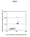
- FIG. 2 shows the relationship between the XRD property of the thin film template substrate and the XRD property of the GaN thick film.
- the property of GaN thick film is influenced by the property of the thin film template substrate.
- the XRD full width at half maximum of the GaN thick film can be not more than 250 seconds, and more preferably, when the XRD full width at half maximum of the thin film template substrate is not more than 200 seconds, the XRD full width at half maximum of the GaN thick film can be not more than 150 seconds.
- the present invention made by the inventors is specifically described based on the embodiment.
- the present invention is not limited to the aforementioned embodiment.
- the distance between the supplying nozzle 5 and the substrate 11 is 100 mm (which is 1.97 times as longer than the diameter of the substrate).
- the similar effect can be obtained when the distance between the supplying nozzle 5 and the substrate 11 is set to be 0.7-4.0 times as longer than the diameter of the substrate.
- the present invention is not limited to the case in which the GaN single crystal is grown, but can also be applied to a case in which a group III-V compound semiconductor single crystal is grown by applying the HVPE method.
- the present invention is not limited to using the NGO substrate as the substrate for growth, but for example, a rare earth group 13 (3B) perovskite crystal, such as NdAlO 3 , NdInO 3 , and the like, may also be applied as the substrate.
- a rare earth group 13 (3B) perovskite crystal such as NdAlO 3 , NdInO 3 , and the like, may also be applied as the substrate.
- the HVPE apparatus which is horizontal is explained, however, the similar effect can be obtained by supplying the group III source material gas (for example, GaCl) through a nozzle, in a vertical HVPE apparatus.
- group III source material gas for example, GaCl
Landscapes
- Chemical & Material Sciences (AREA)
- Engineering & Computer Science (AREA)
- Materials Engineering (AREA)
- Metallurgy (AREA)
- Organic Chemistry (AREA)
- Crystallography & Structural Chemistry (AREA)
- Chemical Kinetics & Catalysis (AREA)
- General Chemical & Material Sciences (AREA)
- Inorganic Chemistry (AREA)
- Mechanical Engineering (AREA)
- Crystals, And After-Treatments Of Crystals (AREA)
- Chemical Vapour Deposition (AREA)
Abstract
Provided are a manufacturing method of a GaN single crystal in which the film thickness of the GaN single crystal can be controlled accurately, even when a hydride vapor phase epitaxy is applied; a GaN thin film template substrate which is suitable for growing a GaN thick film with a fine property; and a GaN single crystal growing apparatus. Provided is a manufacturing method of a GaN single crystal by a hydride vapor phase epitaxy, wherein the hydride vapor phase epitaxy comprises: spraying HCl (hydrogen chloride) onto Ga (gallium) which is heated and fused in a predetermined temperature to generate GaCl (gallium chloride); and forming a GaN thin film by a reaction of the generated GaCl (gallium chloride) with NH3 (ammonia) gas which is hydroxide gas on a substrate, the manufacturing method comprising supplying the NH3 gas in a vicinity of the substrate (for example, at a position which is separated from the substrate by a distance of 0.7-4.0 times as longer than a diameter of the substrate) through a nozzle. Further, as the substrate, an NGO(011) substrate in which the lattice constant thereof is similar to that of GaN is used.
Description
- The present invention relates to a manufacturing method of a GaN single crystal, which is applied with a hydride vapor phase epitaxy, and also related to a GaN single crystal growing apparatus, and a GaN thin film template substrate which is applied to manufacturing a light-emitting device such as a blue LED, and the like.
- Conventionally, as one of the crystal growing methods, a hydride vapor phase epitaxy (HVPE) is known, in which by using a metallic chloride which is generated by a reaction of a heated metallic source material with a hydrogen chloride as source material gas, a crystal is grown from the chloride gas and hydroxide gas of a nonmetallic material.
-
FIG. 3 is a schematic configuration diagram showing the structure of a conventional vapor phase growing apparatus (an HVPE apparatus).
AnHVPE apparatus 100 is configured with a reactingfurnace 1 which is sealed, andresistance heaters 2 which are provided at an outer circumference of the reactingfurnace 1. The reactingfurnace 1 is provided with an HClgas supplying pipe 6 to supply HCl gas to generate a group III source material gas; a group V source material gas supplying pipe 7 to supply group V source material gas such as NH3 gas, and the like, into the reacting furnace; an N2 gas supplying pipe 8 to supply N2 gas into the reacting furnace; agas discharging pipe 3; and a substrate holder 4 to place asubstrate 11. - Further, a source
material placing section 10 is provided in the HClgas supplying pipe 6, and a metallic source material 9 is disposed at this section to generate the group III source material gas. Moreover, the group III source material gas which is generated by the reaction of the HCl gas with the metallic source material 9 is sprayed onto thesubstrate 11 through a supplyingnozzle 12. - In a metal-organic vapor phase epitaxy (MOVPE), a cold-wall heating method is applied, in which only the circumference of the substrate is directly heated, and the wall temperature of the reacting furnace does not rise. On the other hand, as shown in
FIG. 3 , a hot-wall heating method is applied in theHVPE apparatus 100, in which the entire reacting furnace is heated. That is to say, the HVPE method is designed to heat an area from a source material section in which the metallic source material is provided, through a mixing section in which the source material gas is mixed, to a growing section in which the reaction is proceeded so as to grow the crystal. The HVPE method has an advantage in that the crystal can be grown in a relatively high speed by supplying the source material gas on a massive scale. - Generally, in a case where a crystal of a gallium nitride (GaN) is grown by applying the HVPE method, a gallium chloride (GaCl) which is generated by the reaction of a metallic gallium (Ga) with a hydrogen chloride (HCl) is used as the group III source material, and an ammonia (NH3) is used as the group V source material. Here, the thermal decomposition rate of the ammonia is said to be a few %, which is lower compared to that of an arsine (AsH3) which is used as the group V source material when a crystal of a gallium arsenide (GaAs) is grown, and to that of a phosphine (PH3) which is used as the group V source material when a crystal of an indium phosphide (InP) is grown. Accordingly, it is inevitably necessary to enlarge the proportion of V/III which is the supplying proportion of group V source material to the group III source material, when the crystal of GaN single crystal is grown.
- Consequently, when the crystal of GaN single crystal is grown by applying the HVPE method, the following reaction pipe configuration is employed, as shown in
FIG. 3 . That is, a massive NH3 is gradually supplied from the group V source material gas supplying pipe 7, so as to be a laminar flow in the entire reacting furnace, and a small amount of GaCl which is generated by the reaction of the HCl with metallic Ga 9, is sprayed onto thesubstrate 11 in the growing section by thenozzle 12. - Further, Patent Documents 1-5 disclose that a rare earth group 3B perovskite substrate, especially an NGO substrate, is useful for the substrate for growing a GaN system compound semiconductor single crystal.
- Patent Document 1: Japanese Patent Application Laid Open Publication No.
8-186329 - Patent Document 2: Japanese Patent Application Laid Open Publication No.
8-186078 3263891B - Patent Document 3: Japanese Patent Application Laid Open Publication No.
8-208385 3564645B - Patent Document 4: Japanese Patent No.
3293035B - Patent Document 5: Japanese Patent Application Laid Open Publication No.
9-071496 3692452B - Non-Patent Document 1: Journal of Crystal Growth 246 (2002) 215-222
- As described above, in a case where a crystal of GaN single crystal is grown by the conventional HVPE method, a massive NH3 is gradually supplied in the entire reaction pipe so as to be a laminar flow. Accordingly, even when the supply of the source material gas is stopped so as to terminate the crystal growth, GaCl continues to flow out from the Ga surface for a while to react with the NH3 which remains in the reaction pipe, thus GaN is generated. Therefore, it is difficult to accurately control the film thickness and the composition of the GaN single crystal. Incidentally, it is possible to accurately control the film thickness and the composition of the GaN single crystal in the HVPE method, by discharging the gas in the source material section using a vacuum pump, or the like. However, the apparatus becomes extremely complicated in this case.
- As described above, it is difficult to accurately control the film thickness and the composition of the GaN single crystal to be grown in the HVPE method. Thus, the HVPE method has been considered to be unsuitable for manufacturing a GaN thin film template substrate in which an uniformity of film thickness and a high quality of the crystal are required. Accordingly, the GaN thin film template substrate which is currently offered commercially is manufactured mainly by the MBE method or by the MOVPE method.
- By the way, in a case where the GaN thin film template substrate is manufactured by the above mentioned MBE method or the MOCVD method, a sapphire or the like, in which the lattice constant thereof greatly differs from that of GaN is used as the substrate crystal. In such a case, a GaN polycrystal which is referred to as a low temperature buffer layer is grown by approximately 100 nm at 500-600°C on the sapphire substrate, and subsequently, a GaN single crystal is grown by a few micrometers at approximately 1000°C as a template layer, thus the GaN thin film template substrate is manufactured.
However, the above mentioned low temperature buffer layer cannot be subjected to XRD measurement in many cases due to being a polycrystal. Further, even when the low temperature buffer layer can be evaluated, a full width at half maximum thereof is tens of thousands of seconds (Non-Patent Document 1). - The object of the present invention is to provide a manufacturing method of GaN single crystal, in which the film thickness and the composition of the GaN single crystal can be accurately controlled even when the hydride vapor phase epitaxiy is applied, and to provide a GaN thin film template substrate which is suitable for growing a GaN thick film with fine property, and a GaN single crystal growing apparatus.
- The present invention is made in order to solve the above mentioned object, and provided is a manufacturing method of a GaN single crystal by a hydride vapor phase epitaxy, wherein the hydride vapor phase epitaxy comprises: spraying HCl (hydrogen chloride) onto Ga (gallium) which is heated and fused in a predetermined temperature to generate GaCl (gallium chloride); and forming a GaN thin film by a reaction of the generated GaCl (gallium chloride) with NH3 (ammonia) which is hydroxide gas on a substrate, the manufacturing method comprising supplying the NH3 gas in a vicinity of the substrate through a nozzle. Here, the nozzle means a member to squirt fluid at a high speed, and the shape thereof is not particularly limited. Generally, a cylindrical one with a thinned end, or the like, is applied.
- That is to say, by employing the configuration in which the NH3 which is a group V source material is supplied by the nozzle, the starting and stopping of the NH3 supply can be performed instantly, and the NH3 remaining in the reacting furnace after the NH3 supply is stopped is to be reduced.
- To put it concretely, the NH3 gas is supplied at a position which is separated from the substrate by a distance of 0.7-4.0 times as longer than a diameter of the substrate. That is to say, the nozzle to supply the NH3 gas is disposed so that the substrate and the nozzle end are separated from each other by the distance of 0.7-4.0 times as longer than the diameter of the substrate.
- Further, as the substrate, an NGO(011) substrate in which the lattice constant thereof is similar to that of GaN is used. Thereby, a GaN single crystal with high quality, in which for example, the full width at half maximum by the XRD measurement is not more than 1000 seconds, more preferably, the full width at half maximum is not more than 500 seconds, and even more preferably, the full width at half maximum is not more than 200 seconds, can be grown.
- Further, the GaN single crystal growing apparatus (100) according to the present invention, comprises: a reacting furnace (1) which is sealed; a resistance heater (2) which is provided at an outer circumference of the reacting furnace; a GaCl gas supplying section (7, 10) to supply GaCl gas as group III source material gas from a supply port into the reacting furnace; an NH3 gas supplying section (5, 6) to supply NH3 gas as group V source material gas from a supplying nozzle into the reacting furnace; an N2 gas supplying section (8) to supply N2 gas into the reacting furnace; a gas discharging section (3); and a substrate holder (4) to place a substrate, wherein an end of the supplying nozzle is located closer to the substrate than the supply port of the group III source material gas supplying section.
- According to the present invention, the GaN single crystal is grown on the NGO(011) substrate, and subsequently, the supply of the source material gas is stopped instantly, thus superfluous NH3 can be prevented from remaining in the reacting furnace. Thereby, even when GaCl flows out from the surface of the Ga source material, reaction with NH3 does not happen after the supply of the source material gas is stopped. Accordingly, the growth of the GaN single crystal can reliably be prevented from proceeding, and the film thickness of the GaN single crystal can be controlled extremely accurately (for example, in a nanometer order) even when the HVPE method is applied. Further, because the HVPE method is applied, the GaN single crystal can be grown in a relatively high speed, and the manufacturing cost of the GaN single crystal can be reduced.
- Moreover, in the GaN thin film template which can be obtained by the above described manufacturing method, the full width at half maximum by the XRD measurement is to be not more than 1000 seconds, thus the GaN thin film template can stably exist even when heated to approximately 1000°C which is a general growing temperature of the GaN single crystal. As a result, a GaN thick film with high quality can be formed by using the GaN thin film template, thus can realize a light-emitting device such as a blue LED, and the like, with excellent property.
-
- [
FIG. 1 ] This is a schematic configuration diagram showing a structure of a vapor phase growing apparatus (an HVPE apparatus) according to an embodiment. - [
FIG. 2 ] This is an explanatory diagram showing a relationship between an XRD property of a thin film template substrate and an XRD property of a GaN thick film. - [
FIG. 3 ] This is a schematic configuration diagram showing a structure of a conventional vapor phase growing apparatus (an HVPE apparatus). - Hereinbelow, a preferred embodiment will be explained with reference to the drawings.
FIG. 1 is a schematic configuration diagram showing the structure of a vapor phase growing apparatus (an HVPE apparatus) according to the embodiment.
TheHVPE apparatus 100 is configured with a reactingfurnace 1 which is sealed, andresistance heaters 2 which are provided at an outer circumference of the reactingfurnace 1. The reactingfurnace 1 is provided with an HCl gas supplying pipe 7 to supply HCl gas to generate a group III source material gas; a group V source materialgas supplying pipe 6 to supply group V source material gas such as NH3 gas, and the like, into the reacting furnace; an N2 gas supplying pipe 8 to supply N2 gas into the reacting furnace; agas discharging pipe 3; and a substrate holder 4 to place asubstrate 11. - A source
material placing section 10 is provided in the HClgas supplying pipe 6, and a metallic source material 9 is disposed at this section to generate the group III source material gas. Moreover, in the present embodiment, a supplyingnozzle 5 is provided at the end of the group V source materialgas supplying pipe 6, so that the NH3 gas is sprayed onto thesubstrate 11 through the supplyingnozzle 5. - Here, the supplying
nozzle 5 is provided so that the end thereof is closer to the substrate than the supply port provided at the sourcematerial placing section 10. For example, the supplyingnozzle 5 is provided so that the substrate and the end of the supplyingnozzle 5 are separated from each other by the distance of 0.7-4.0 times as longer than the diameter of the substrate. - Next, a case in which a GaN single crystal is grown by using the above described
HVPE apparatus 100 is explained in detail.
In the present embodiment, an NGO(011) in which the lattice constant thereof is similar to that of GaN is used as the substrate for crystal growth. Further, the group III source material gas is GaCl which is generated from metallic Ga and HCl, and the group V source material gas is NH3. Moreover, in theHVPE apparatus 100, the distance between the supplyingnozzle 5 and thesubstrate 11 is 100 mm (which is 1.97 times as longer than the diameter of the substrate).
First, an ingot of the NGO(011) is sliced so as to make the substrate for the crystal growth. On this occasion, the diameter of the NGO substrate is 2 inches, and the thickness thereof is 350 µm. - Next, the NGO substrate is subjected to a mirror polish, and further subjected to the surface treatments in the following procedures as necessary. That is to say, the NGO substrate is performed with an ultrasonic cleansing by acetone, then by methanol for 5 minutes, respectively. Subsequently, the substrate is blown by nitrogen gas so as to blow off the droplets, then is dried naturally. Further, the substrate is subjected to an etching for 5 minutes by a sulfuric acid system etchant (for example, phosphoric acid : sulfuric acid = 1 : 3 (proportion in volume), 80°C).
- Subsequently, after the
NGO substrate 11 is disposed on a predetermined position of the substrate holder 4, the substrate temperature is increased to 600°C in a state where N2 gas is introduced thereto through the N2 gas supplying pipe 8. Subsequently, HCl gas is introduced through the HClgas supplying pipe 6, and GaCl is generated by the reaction of metallic Ga 9 with HCl, so as to supply the generated GaCl onto theNGO substrate 11. Further, NH3 gas is supplied onto theNGO substrate 11 from the NH3 gas supplying pipe 7 through the supplyingnozzle 5. On this occasion, N2 gas is applied as the carrier gas. - Further, the GaN compound semiconductor crystal is grown in a growth rate of approximately 0.72 µm/h in a state of controlling the gas introduction amount so that the partial pressure of GaCl be 0.002 atm, and the partial pressure of NH3 be 0.066 atm, respectively.
- In the present embodiment, the group V source material gas (NH3) is supplied in the vicinity of the NGO(011)
substrate 11 through the nozzle, thus the supply of the source material gas can instantly be stopped after the growth of the GaN single crystal is terminated. Thereby, the NH3 can be prevented from remaining in the reacting furnace after the supply of the source material gas is stopped, and reaction does not happen even when GaCl flows out from the surface of the Ga source material. Thus, the growth of the GaN single crystal can reliably be prevented from proceeding after the supply of the source material gas is stopped. - On the other hand, in the conventional apparatus configuration (see
FIG. 3 ), even when the source material gas (HCl) is stopped, due to the GaCl which is supplied to just proximal to the substrate through the nozzle being small in flow amount, the remaining GaCl in the nozzle continues to flow out for a while, and it is difficult to stop the growth instantly. - Tables 1 and 2 show the measurement results of film thickness and full width at half maximum by XRD (X-ray diffraction) at 5 points in the wafer surface of the GaN single crystal thin film which is obtained by the above described manufacturing method. Incidentally, table 1 is a measurement result pertaining to GaN single crystal A which is grown in a state where the film thickness is controlled to be 60 nm, and table 2 is a measurement result pertaining to GaN single crystal B which is grown in a state where the film thickness is controlled to be 65 nm.
- As shown in table 1, in GaN single crystal A, the difference between the maximum film thickness and the minimum film thickness is 4.298 nm, and error from the controlled film thickness is 1.677-2.621 nm. Further, as shown in table 2, in GaN single crystal B, the difference between the maximum film thickness and the minimum film thickness is 3.340 nm, and error from the controlled film thickness is 2.365-0.975 nm. From these results, it can be confirmed that the film thickness of GaN single crystal can be controlled accurately and uniformly in the manufacturing method applying the HVPE method.
- Further, the full width at half maximum by the XRD of either of GaN single crystals A and B is not more than 200 seconds. Thereby, it can be said that the GaN single crystal thin film which is grown on the NGO(011) substrate is extremely superior in crystal property, thus is extremely effective as a GaN thin film template substrate for growing the GaN thick film.
- As described above, in the present embodiment, because the NGO(011) substrate in which the lattice constant thereof is similar to that of GaN is used, a GaN single crystal with high quality can be grown. Further, the GaN single crystal is grown on the NGO substrate, and after the supply of the source material gas is stopped, the NH3 can be prevented from remaining in the reacting furnace. Thus, even when GaCl flows out from the surface of the Ga source material, reaction does not happen. Accordingly, the growth of the GaN single crystal can reliably be prevented from proceeding after the source material gas is stopped, and the film thickness of GaN single crystal can be controlled extremely accurately even when HVPE method is applied.
-
[Table 1] GaN single crystal A MEASUREMENT POINT XRD FULL WIDTH AT HALF MAXIMUM (seconds) FILM THICKNESS (nm) 1 159 58.323 2 162 61.869 3 146 62.621 4 151 59.527 5 151 58.407 -
[Table 2] GaN single crystal B MEASUREMENT POINT XRD FULL WIDTH AT HALF MAXIMUM (seconds) FILM THICKNESS (nm) 1 162 63.664 2 184 65.975 3 153 65.299 4 148 65.064 5 151 62.635 - Next, the above described GaN single crystal A (B) is used as the GaN thin film template substrate, and for example, GaN thick film is grown on the substrate by HVPE method by 500 µm. Table 3 shows the XRD property of the GaN thick film formed on the GaN thin film template substrate.
- As shown in Table 3, by applying the GaN thin film template substrate which is obtained by the manufacturing method according to the present embodiment, the full width at half maximum by XRD of the grown GaN thick film can be controlled so as to be not more than 200 seconds. By the application of the GaN thick film having such XRD property, a light-emitting device such as a blue LED, and the like having an excellent property, can be realized.
-
[Table 3] GaN single crystal grown with GaN single crystal A as a template substrate MEASUREMENT POINT XRD FULL WIDTH AT HALF MAXIMUM (seconds) 1 88 2 90 3 108 4 157 5 124 -
FIG. 2 shows the relationship between the XRD property of the thin film template substrate and the XRD property of the GaN thick film. As shown inFIG. 2 , the property of GaN thick film is influenced by the property of the thin film template substrate.
To put it concretely, in order to obtain a GaN thick film with high quality (for example, XRD full width at half maximum of not more than 1000 seconds), it is required that the full width at half maximum of the thin film template substrate be not more than 1000 seconds. Preferably, when the full width at half maximum of the thin film template substrate is not more than 500 seconds, the XRD full width at half maximum of the GaN thick film can be not more than 250 seconds, and more preferably, when the XRD full width at half maximum of the thin film template substrate is not more than 200 seconds, the XRD full width at half maximum of the GaN thick film can be not more than 150 seconds. - As described above, the present invention made by the inventors is specifically described based on the embodiment. However, the present invention is not limited to the aforementioned embodiment.
For example, in the above mentioned embodiment, the distance between the supplyingnozzle 5 and thesubstrate 11 is 100 mm (which is 1.97 times as longer than the diameter of the substrate). However, the similar effect can be obtained when the distance between the supplyingnozzle 5 and thesubstrate 11 is set to be 0.7-4.0 times as longer than the diameter of the substrate. - Further, the present invention is not limited to the case in which the GaN single crystal is grown, but can also be applied to a case in which a group III-V compound semiconductor single crystal is grown by applying the HVPE method.
- Further, the present invention is not limited to using the NGO substrate as the substrate for growth, but for example, a rare earth group 13 (3B) perovskite crystal, such as NdAlO3, NdInO3, and the like, may also be applied as the substrate.
- Further, in the embodiment, the HVPE apparatus which is horizontal is explained, however, the similar effect can be obtained by supplying the group III source material gas (for example, GaCl) through a nozzle, in a vertical HVPE apparatus.
Claims (7)
- A manufacturing method of a GaN single crystal by a hydride vapor phase epitaxy, wherein
the hydride vapor phase epitaxy comprises:spraying HCl (hydrogen chloride) onto Ga (gallium) which is heated and fused in a predetermined temperature to generate GaCl (gallium chloride); andforming a GaN thin film by a reaction of the generated GaCl (gallium chloride) with NH3 (ammonia) gas on a substrate,the manufacturing method comprising supplying the NH3 gas in a vicinity of the substrate through a nozzle. - The manufacturing method of the GaN single crystal as claimed in claim 1, wherein the NH3 gas is supplied at a position which is separated from the substrate by a distance of 0.7-4.0 times as longer than a diameter of the substrate.
- The manufacturing method of the GaN single crystal as claimed in claim 1 or 2, wherein the substrate is an NGO(011) substrate.
- A GaN thin film template substrate which is obtained by the manufacturing method as claimed in any one of claims 1-3, wherein a full width at half maximum of the GaN thin film template by an XRD measurement is not more than 1000 seconds.
- The GaN thin film template substrate as claimed in claim 4, wherein the full width at half maximum by the XRD measurement is not more than 500 seconds.
- The GaN thin film template substrate as claimed in claim 5, wherein the full width at half maximum by the XRD measurement is not more than 200 seconds.
- A GaN single crystal growing apparatus, comprising:a reacting furnace which is sealed;a resistance heater which is provided at an outer circumference of the reacting furnace;a GaCl gas supplying section to supply GaCl gas as group III source material gas from a supply port into the reacting furnace;an NH3 gas supplying section to supply NH3 gas as group V source material gas from a supplying nozzle into the reacting furnace;an N2 gas supplying section to supply N2 gas into the reacting furnace;a gas discharging section; anda substrate holder to place a substrate, whereinan end of the supplying nozzle is located closer to the substrate than the supply port of the GaCl gas supplying section.
Applications Claiming Priority (2)
| Application Number | Priority Date | Filing Date | Title |
|---|---|---|---|
| JP2006253797 | 2006-09-20 | ||
| PCT/JP2007/067942 WO2008035632A1 (en) | 2006-09-20 | 2007-09-14 | PROCESS FOR PRODUCING GaN SINGLE-CRYSTAL, GaN THIN-FILM TEMPLATE SUBSTRATE AND GaN SINGLE-CRYSTAL GROWING APPARATUS |
Publications (2)
| Publication Number | Publication Date |
|---|---|
| EP2065489A1 true EP2065489A1 (en) | 2009-06-03 |
| EP2065489A4 EP2065489A4 (en) | 2010-12-15 |
Family
ID=39200458
Family Applications (1)
| Application Number | Title | Priority Date | Filing Date |
|---|---|---|---|
| EP07807346A Withdrawn EP2065489A4 (en) | 2006-09-20 | 2007-09-14 | METHOD FOR MANUFACTURING GaN MONOCRYSTAL, GaN THIN FILM MATRIX SUBSTRATE, AND GaN MONOCRYSTAL GROWTH APPARATUS |
Country Status (7)
| Country | Link |
|---|---|
| US (1) | US8137460B2 (en) |
| EP (1) | EP2065489A4 (en) |
| JP (1) | JPWO2008035632A1 (en) |
| KR (1) | KR20090053827A (en) |
| CN (1) | CN101517134A (en) |
| TW (1) | TW200823974A (en) |
| WO (1) | WO2008035632A1 (en) |
Families Citing this family (7)
| Publication number | Priority date | Publication date | Assignee | Title |
|---|---|---|---|---|
| DE102007010286B4 (en) | 2007-03-02 | 2013-09-05 | Freiberger Compound Materials Gmbh | A method for producing a compound semiconductor material, a III-N layer or a III-N bulk crystal, a reactor for producing the compound semiconductor material, compound semiconductor material, III-N bulk crystal and III-N crystal layer |
| CN102245814A (en) * | 2010-02-01 | 2011-11-16 | 吉坤日矿日石金属株式会社 | Manufacturing method of nitride-based compound semiconductor substrate and nitride-based compound semiconductor self-supporting substrate |
| CN107085003B (en) * | 2017-05-02 | 2020-03-17 | 合肥工业大学 | X-ray diffraction in-situ characterization method for film oriented crystal growth |
| KR102040180B1 (en) * | 2018-04-30 | 2019-11-05 | 에임즈마이크론 주식회사 | Apparatus for Sampling Ga and Method for Sampling Ga |
| JP7372059B2 (en) * | 2019-06-27 | 2023-10-31 | 株式会社トクヤマ | Method for manufacturing group III nitride single crystal |
| KR102546042B1 (en) * | 2021-12-22 | 2023-06-22 | 주식회사루미지엔테크 | Ga2O3 crystal film deposition method according to HVPE, deposition apparatus and Ga2O3 crystal film deposition substrate using the same |
| WO2025004367A1 (en) * | 2023-06-30 | 2025-01-02 | 株式会社Kokusai Electric | Substrate processing device, gas supply unit, substrate processing method, production method for semiconductor device, and program |
Family Cites Families (14)
| Publication number | Priority date | Publication date | Assignee | Title |
|---|---|---|---|---|
| EP0711853B1 (en) | 1994-04-08 | 1999-09-08 | Japan Energy Corporation | Method for growing gallium nitride compound semiconductor crystal, and gallium nitride compound semiconductor device |
| JP3263891B2 (en) | 1994-12-28 | 2002-03-11 | 株式会社ジャパンエナジー | Gallium nitride based semiconductor crystal growth method |
| JPH08186329A (en) | 1994-12-28 | 1996-07-16 | Japan Energy Corp | Method for growing gallium nitride based semiconductor crystal |
| JP3564645B2 (en) | 1995-01-27 | 2004-09-15 | 株式会社日鉱マテリアルズ | Gallium nitride based semiconductor crystal growth method |
| JP3692452B2 (en) | 1995-09-07 | 2005-09-07 | 株式会社日鉱マテリアルズ | Method for producing gallium nitride single crystal thick film |
| JP3292083B2 (en) * | 1997-03-11 | 2002-06-17 | 日亜化学工業株式会社 | Method for manufacturing nitride semiconductor substrate and method for manufacturing nitride semiconductor element |
| JP3631724B2 (en) * | 2001-03-27 | 2005-03-23 | 日本電気株式会社 | Group III nitride semiconductor substrate and manufacturing method thereof |
| JP2002305155A (en) * | 2001-04-09 | 2002-10-18 | Nikko Materials Co Ltd | CRYSTAL GROWING APPARATUS FOR GaN-BASED COMPOUND SEMICONDUCTOR CRYSTAL |
| JP2003063897A (en) * | 2001-08-28 | 2003-03-05 | Sony Corp | Nitride III-V compound semiconductor substrate, method of manufacturing the same, method of manufacturing semiconductor light emitting element, and method of manufacturing semiconductor device |
| JP4150527B2 (en) * | 2002-02-27 | 2008-09-17 | 日鉱金属株式会社 | Crystal production method |
| US7781356B2 (en) * | 2003-02-12 | 2010-08-24 | Arizona Board of Regents, a Body Corporate | Epitaxial growth of group III nitrides on silicon substrates via a reflective lattice-matched zirconium diboride buffer layer |
| JP2005001928A (en) * | 2003-06-11 | 2005-01-06 | Fujikura Ltd | Self-standing substrate and manufacturing method thereof |
| JP5374872B2 (en) * | 2006-03-29 | 2013-12-25 | 住友電気工業株式会社 | Group III nitride single crystal growth method |
| JP4959468B2 (en) * | 2006-09-08 | 2012-06-20 | 株式会社トクヤマ | Group III nitride production method and apparatus |
-
2007
- 2007-09-14 JP JP2008535337A patent/JPWO2008035632A1/en active Pending
- 2007-09-14 KR KR1020097005555A patent/KR20090053827A/en not_active Withdrawn
- 2007-09-14 CN CNA2007800349256A patent/CN101517134A/en active Pending
- 2007-09-14 WO PCT/JP2007/067942 patent/WO2008035632A1/en not_active Ceased
- 2007-09-14 US US12/441,483 patent/US8137460B2/en not_active Expired - Fee Related
- 2007-09-14 EP EP07807346A patent/EP2065489A4/en not_active Withdrawn
- 2007-09-19 TW TW096134903A patent/TW200823974A/en unknown
Also Published As
| Publication number | Publication date |
|---|---|
| TW200823974A (en) | 2008-06-01 |
| CN101517134A (en) | 2009-08-26 |
| US8137460B2 (en) | 2012-03-20 |
| KR20090053827A (en) | 2009-05-27 |
| EP2065489A4 (en) | 2010-12-15 |
| JPWO2008035632A1 (en) | 2010-01-28 |
| US20090294774A1 (en) | 2009-12-03 |
| WO2008035632A1 (en) | 2008-03-27 |
Similar Documents
| Publication | Publication Date | Title |
|---|---|---|
| EP1997125B1 (en) | Growth method using nanocolumn compliant layers and hvpe for producing high quality compound semiconductor materials | |
| KR101547144B1 (en) | Method and device for the production of a compound semiconductor material by means of gas phase epitaxy | |
| JP7255817B2 (en) | GaN crystal manufacturing method | |
| EP2037013B1 (en) | Method for preparing substrate for growing gallium nitride and method for preparing gallium nitride substrate | |
| US8137460B2 (en) | Manufacturing method of GaN thin film template substrate, GaN thin film template substrate and GaN thick film single crystal | |
| US6500258B2 (en) | Method of growing a semiconductor layer | |
| EP1801269A1 (en) | Process for producing a free-standing III-N layer, and free-standing III-N substrate | |
| JP2004006568A (en) | Method for manufacturing group 3-5 compound semiconductor | |
| US10707309B2 (en) | GaN laminate and method of manufacturing the same | |
| US20100272141A1 (en) | Nitride semiconductor freestanding substrate and manufacturing method of the same, and laser diode | |
| KR101335937B1 (en) | Method for fabricating gan wafer using llo(laser lift-off) process | |
| US20100101486A1 (en) | Substrate for epitaxial growth and method for producing nitride compound semiconductor single crystal | |
| KR100975835B1 (en) | Method for manufacturing nanostructure at low temperature using indium | |
| KR100949212B1 (en) | Nitride substrate manufacturing method | |
| KR100472626B1 (en) | Apparatus for manufacturing GaN thick layer | |
| KR102086725B1 (en) | Nitride semiconductor free-standing substrate, and method and apparatus for manufacturing the same | |
| KR101007501B1 (en) | Nanostructure Manufacturing Method Using Hydrogen Chloride Flow Control | |
| KR20080099545A (en) | Nanorod manufacturing method using etching gas | |
| JP2001168050A (en) | Method of growing III-V compound semiconductor | |
| TW201205678A (en) | Method for producing nitride compound semiconductor substrate, nitride compound semiconductor substrate and self-supporting nitride compound semiconductor substrate | |
| KR20080088126A (en) | Nanostructure manufacturing apparatus and nanostructure manufacturing method capable of local temperature control of substrate | |
| JP2012224486A (en) | Method for producing group 13 nitride crystal | |
| KR20090083601A (en) | Method for manufacturing gallium nitride nanostructure at low temperature using flow rate control of hydrogen chloride gas |
Legal Events
| Date | Code | Title | Description |
|---|---|---|---|
| PUAI | Public reference made under article 153(3) epc to a published international application that has entered the european phase |
Free format text: ORIGINAL CODE: 0009012 |
|
| 17P | Request for examination filed |
Effective date: 20090330 |
|
| AK | Designated contracting states |
Kind code of ref document: A1 Designated state(s): DE FR GB |
|
| AX | Request for extension of the european patent |
Extension state: AL BA HR MK RS |
|
| A4 | Supplementary search report drawn up and despatched |
Effective date: 20101117 |
|
| 17Q | First examination report despatched |
Effective date: 20120217 |
|
| DAX | Request for extension of the european patent (deleted) | ||
| STAA | Information on the status of an ep patent application or granted ep patent |
Free format text: STATUS: THE APPLICATION IS DEEMED TO BE WITHDRAWN |
|
| 18D | Application deemed to be withdrawn |
Effective date: 20140401 |