EP2063449A1 - Method for obtaining a scanning transmission image of a sample in a particle-optical apparatus - Google Patents
Method for obtaining a scanning transmission image of a sample in a particle-optical apparatus Download PDFInfo
- Publication number
- EP2063449A1 EP2063449A1 EP08169468A EP08169468A EP2063449A1 EP 2063449 A1 EP2063449 A1 EP 2063449A1 EP 08169468 A EP08169468 A EP 08169468A EP 08169468 A EP08169468 A EP 08169468A EP 2063449 A1 EP2063449 A1 EP 2063449A1
- Authority
- EP
- European Patent Office
- Prior art keywords
- sample
- focused beam
- angle
- finely focused
- over
- Prior art date
- Legal status (The legal status is an assumption and is not a legal conclusion. Google has not performed a legal analysis and makes no representation as to the accuracy of the status listed.)
- Granted
Links
Images

Classifications
-
- H—ELECTRICITY
- H01—ELECTRIC ELEMENTS
- H01J—ELECTRIC DISCHARGE TUBES OR DISCHARGE LAMPS
- H01J37/00—Discharge tubes with provision for introducing objects or material to be exposed to the discharge, e.g. for the purpose of examination or processing thereof
- H01J37/26—Electron or ion microscopes; Electron or ion diffraction tubes
- H01J37/261—Details
- H01J37/263—Contrast, resolution or power of penetration
-
- H—ELECTRICITY
- H01—ELECTRIC ELEMENTS
- H01J—ELECTRIC DISCHARGE TUBES OR DISCHARGE LAMPS
- H01J37/00—Discharge tubes with provision for introducing objects or material to be exposed to the discharge, e.g. for the purpose of examination or processing thereof
- H01J37/26—Electron or ion microscopes; Electron or ion diffraction tubes
- H01J37/261—Details
- H01J37/265—Controlling the tube; circuit arrangements adapted to a particular application not otherwise provided, e.g. bright-field-dark-field illumination
-
- H—ELECTRICITY
- H01—ELECTRIC ELEMENTS
- H01J—ELECTRIC DISCHARGE TUBES OR DISCHARGE LAMPS
- H01J37/00—Discharge tubes with provision for introducing objects or material to be exposed to the discharge, e.g. for the purpose of examination or processing thereof
- H01J37/26—Electron or ion microscopes; Electron or ion diffraction tubes
- H01J37/28—Electron or ion microscopes; Electron or ion diffraction tubes with scanning beams
-
- H—ELECTRICITY
- H01—ELECTRIC ELEMENTS
- H01J—ELECTRIC DISCHARGE TUBES OR DISCHARGE LAMPS
- H01J2237/00—Discharge tubes exposing object to beam, e.g. for analysis treatment, etching, imaging
- H01J2237/26—Electron or ion microscopes
- H01J2237/28—Scanning microscopes
- H01J2237/2802—Transmission microscopes
-
- H—ELECTRICITY
- H01—ELECTRIC ELEMENTS
- H01J—ELECTRIC DISCHARGE TUBES OR DISCHARGE LAMPS
- H01J2237/00—Discharge tubes exposing object to beam, e.g. for analysis treatment, etching, imaging
- H01J2237/26—Electron or ion microscopes
- H01J2237/28—Scanning microscopes
- H01J2237/2803—Scanning microscopes characterised by the imaging method
-
- H—ELECTRICITY
- H01—ELECTRIC ELEMENTS
- H01J—ELECTRIC DISCHARGE TUBES OR DISCHARGE LAMPS
- H01J2237/00—Discharge tubes exposing object to beam, e.g. for analysis treatment, etching, imaging
- H01J2237/26—Electron or ion microscopes
- H01J2237/28—Scanning microscopes
- H01J2237/2809—Scanning microscopes characterised by the imaging problems involved
Definitions
- STEM a sample is scanned by a finely focused beam of electrons.
- the electrons have an energy of typically between 80 and 300 keV. Some of the electrons are absorbed by the sample, some are scattered in the sample and some electrons pass through the sample unhindered. The electrons passing through the sample (scattered and unscattered electrons) are detected by an electron detector. In this way it is possible to get a 2D image of the sample.
- the method according to the invention is characterized in that the thickness T of the sample is determined, the length L of the sample material through which the transmitted particles have to travel is derived from the thickness T of the sample, and the opening half-angle is set to a value ⁇ such that 0.5 ⁇ R( ⁇ ) / L ⁇ tan( ⁇ ) ⁇ 2 - R( ⁇ ) / L, as a result of which the sample is scanned with a beam having a substantially constant diameter over a length equal to the length L of the sample material through which the transmitted particles have to travel.
- the minimum beam diameter depends on the accelerating voltage and several parameters of the instrument used.
- commercial instruments are available that achieve a STEM resolution below 0.1 nm using opening angles in excess of 10 mrad, such as the Titan TM 80-300 of FEI Company, Hillsboro, USA.
- Such a resolution is obtained using very thin samples of e.g. less than 50 nm thick.
- the sample is substantially perpendicular to the finely focused beam and the length L of the sample material through which the transmitted particles have to travel equals the thickness T of the sample, and the opening half-angle ⁇ of the finely focused beam is set to a value ⁇ such that 0.5 ⁇ R( ⁇ ) / T ⁇ tan( ⁇ ) ⁇ 2 ⁇ R( ⁇ ) / T .
- the cross-over is located substantially halfway the two surfaces.
- the focal length of the lens focusing the finely focused beam is changed during the scanning of the beam over the sample so as to compensate for the tilting of the sample relative to the finely focused beam, thereby keeping the distance of the cross-over with respect to a surface of the sample substantially constant.
- the cross-over diameter R( ⁇ ) is approximately equal to the diameter D, and therefore a balance between the contributions due to cross-over diameter and convergence angle occurs at the corresponding opening half-angles.
- the maximum diameter of the beam is now approximately 0.4 nm, a factor two lower than when using the opening half-angle giving the optimum cross-over diameter.
- the maximum diameter is now only approximately 0.8 nm instead of 4 nm, an improvement of approximately 5 times when compared to the maximum beam diameter at 8 mrad, although 5 times worse than the cross-over diameter of 0.15 nm at 8 mrad, i.e. the resolution that can be achieved for very thin samples..
- the opening angle of the beam impinging on the sample is set by the focal length of the objective lens 505 (which for a given instrument is a largely fixed value), the magnification of the condenser lenses 504 and the size of the aperture in diaphragm 503.
Landscapes
- Chemical & Material Sciences (AREA)
- Analytical Chemistry (AREA)
- Analysing Materials By The Use Of Radiation (AREA)
- Investigating Or Analysing Materials By Optical Means (AREA)
Abstract
Description
- The invention relates to a method for obtaining a scanning transmission image of a sample in a particle-optical apparatus, said apparatus equipped to image a sample by scanning the sample with a finely focused beam of particles and detecting particles transmitted through the sample, said finely focused beam showing a smallest diameter, the so-named cross-over, the diameter of the cross-over R being a function of the opening half-angle α of the finely focused beam, the method comprising:
- acquiring an image of the sample by scanning the sample with the finely focused beam of particles and detecting particles transmitted through the sample,
The invention further relates to software to obtain such images. - Such a method is known from "Recent advances in Electron Tomography: TEM and HAADF-STEM Tomography for materials science and IC applications", C. Kubel et al., Microscopy and Microanalysis, 2005, Vol. 11, . In this publication a method known as STEM (Scanning Transmission Electron Microscopy) tomography is described.
- In STEM a sample is scanned by a finely focused beam of electrons. The electrons have an energy of typically between 80 and 300 keV. Some of the electrons are absorbed by the sample, some are scattered in the sample and some electrons pass through the sample unhindered. The electrons passing through the sample (scattered and unscattered electrons) are detected by an electron detector. In this way it is possible to get a 2D image of the sample.
- To study certain features such as catalysts, macro-molecules or structures in biological tissue in samples, it is often desired to make a 3D representation of said features. To obtain such a 3D representation a series of 2D images of the sample at different tilt angles is combined in a 3D tomogram.
- For optimum resolution in a STEM extremely thin samples are used. Resolutions of less than 0.1 nm can be obtained for samples thinner than 50 nm. As known to the person skilled in the art a thicker sample, e.g. a sample thicker than 100 nm, can not be imaged with such a high resolution. Especially when the sample is tilted as well, as is being done during STEM tomography, the effective thickness of the sample limits the resolution.
- There is a need for a method to improve the resolution of images of thick samples.
- To that end the method according to the invention is characterized in that the thickness T of the sample is determined, the length L of the sample material through which the transmitted particles have to travel is derived from the thickness T of the sample, and the opening half-angle is set to a value α such that 0.5 · R(α) / L ≤ tan(α) ≤ 2 - R(α) / L, as a result of which the sample is scanned with a beam having a substantially constant diameter over a length equal to the length L of the sample material through which the transmitted particles have to travel.
- As known to the person skilled in the art the diameter of the cross-over depends on the opening half-angle of the beam. This is explained in e.g. "Transmission Electron Microscopy", L. Reimer, Springer Verlag, 4th ed., ISBN 3-540-62568-2. In section 4.2.2 of said handbook, more specifically in formula 4.18 and
figure 4.13 , it is shown that the diameter of the cross-over is a function of the opening half-angle of the beam, that a minimum diameter of the cross-over occurs for a certain opening half-angle, while smaller and larger opening half-angles result in larger cross-over diameters. For best resolution the person skilled in the art will thus select the opening half-angle resulting in the optimum resolution. - It is noted that the minimum beam diameter depends on the accelerating voltage and several parameters of the instrument used. Nowadays commercial instruments are available that achieve a STEM resolution below 0.1 nm using opening angles in excess of 10 mrad, such as the Titan™ 80-300 of FEI Company, Hillsboro, USA. Such a resolution is obtained using very thin samples of e.g. less than 50 nm thick.
- The method according to the invention is based on the insight that the beam for an optimum opening half-angle may show an optimum for the diameter of the cross-over, e.g. a diameter of 0.1 nm, but that the diameter of the beam elsewhere in the sample has a much larger diameter due to the opening half-angle used. For a sample with a thickness of e.g. 500 nm, and an opening half-angle of e.g. 10 mrad, the diameter of the
beam 250 nm removed from the cross-over is 5 nm. Therefore the resolution in part of the sample is not close to 0.1 nm, but more than 10 times larger. Reducing the opening half-angle results in a larger diameter of the cross-over, but the beam diameter at a position removed from the cross-over is reduced. By selecting an opening half-angle in which the broadening of the cross-over is balanced with the broadening of the beam inside the sample as a result of the opening angle, an image with optimum overall resolution is obtained. - It is noted that this method resembles the method known as microbeam TEM, where a parallel beam with small diameter (typically several micrometers) is generated to illuminate a part of the sample. This makes it possible to obtain e.g. crystallographic information of micro-crystallites by studying the diffraction pattern of the transmitted electrons. Here the beam diameter is not limited by the beam aberrations as explained in the book of Reimer mentioned before, but is governed by the demand that it is a parallel beam, necessary for diffraction. Also, the microbeam is not scanned over the sample, but instead a selected area is selected by positioning the microbeam on the selected area, after which an image, such as a diffraction image, is made thereof, or an X-ray analysis of the selected area is made.
- It is further noted that the method also resembles the method known as nanobeam STEM, in which a small cross-over is scanned over the sample. Here the opening half-angle is optimized for minimal diameter of the cross-over, as explained before. The method according to the invention differs from nanobeam STEM in that the opening half-angle is optimised to overall beam diameter instead of only the cross-over diameter.
- In an embodiment of the method according to the invention the sample is substantially perpendicular to the finely focused beam and the length L of the sample material through which the transmitted particles have to travel equals the thickness T of the sample, and the opening half-angle α of the finely focused beam is set to a value α such that 0.5 · R(α) / T ≤ tan(α ) ≤ 2 · R(α) / T .
- When the sample is perpendicular to the beam, also known as the non-tilted position, the length L equals the thickness of the sample.
- It is noted that the angle under which the beam impinges on the sample is virtually unchanged during scanning. The beam is scanned over the sample by deflecting the beam by a deflection unit, the deflection unit normally deflecting the beam with an electric or magnetic field. The area over which the beam is scanned is much smaller than the distance between the scan unit and the sample, so that the angle under which the beam impinges is virtually independent on the deflection of the beam.
- In another embodiment of the method according to the invention the sample is tilted to an angle β with respect to the finely focused beam before the image is acquired, as a result of which the length L of the sample material through which the transmitted particles have to travel equals the thickness T of the sample multiplied by the cosine of the tilt angle β, and the opening half-angle α of the finely focused beam is set to a value α such that 0.5 · R(α) · cos (β) / T ≤ tan(α ) ≤ 2 · R(α) · cos (β) / T.
- When the sample is tilted, the beam impinges on the sample under an angle. The particles transmitted through the sample have to travel though a larger amount of material.
- In yet another embodiment of the method according to the invention the method further comprises determining a maximum tilt angle βmax and a number of images to be acquired, determining the maximum length Lmax of the sample material through which the transmitted particles have to travel, Lmax = T / cos (βmax), setting the opening half-angle α of the finely focused beam to a value α such that 0.5 · R(α) α cos (βmax) / T ≤ tan(α ) ≤ 2 · R(α) · cos (βmax) / T, acquiring a series of images at different tilt angles, each of the different tilt angles being equal to or less than the maximum tilt angle βmax, and combining said series of images in a 3D reconstruction of the bulk information of the sample.
- In STEM tomography a series of images is acquired under different tilt angles, e.g. under a tilt ranging from -70 degrees to +70 degrees with increments of 2 degrees. As a result the maximum length of material through which the particles have to travel occurs for the most tilted positions.
- In still another embodiment of the method according to the invention the sample shows two substantially flat surfaces and the cross-over is located between said surfaces.
- This describes that the cross-over is imaged between the surfaces of the sample, i.e. in the sample.
- In a further embodiment of the method according to the invention the cross-over is located substantially halfway the two surfaces.
- In another embodiment of the method according to the invention the focal length of the lens focusing the finely focused beam is changed during the scanning of the beam over the sample so as to compensate for the tilting of the sample relative to the finely focused beam, thereby keeping the distance of the cross-over with respect to a surface of the sample substantially constant.
- In this embodiment the distance of the cross-over to the surface of the sample is kept constant while scanning the beam over the sample. This is also known as "dynamic focus".
- In yet another embodiment of the method according to the invention the thickness of the sample is larger than 100 nm.
- Especially for thick sample the invention offers an improved resolution. As mentioned before, conventional STEM uses an opening half-angle of e.g. 10 mrad, for a 100 nm thick sample resulting in a diameter of the beam of 0.5 nm when the cross-over is positioned halfway the sample surfaces. For a thickness of 100 nm and more a much improved resolution can be achieved using the method according to the invention.
- In a further embodiment of the method according to the invention the thickness of the sample is larger than 1000 nm.
- In yet another embodiment of the method according to the invention the apparatus is a scanning transmission electron microscope.
- STEM is a well known technique that can benefit from the invention, although the invention is also applicable to other techniques using e.g. hydrogen particles, ions, etc.
- In still another embodiment of the method according to the invention the sample is an amorphous sample.
- The invention is especially beneficial to samples comprising features such as catalysts, macro-molecules or structures in biological tissue in samples embedded in an amorphous matrix.
- In an aspect of the invention software for programming a programmable controller of a particle-optical apparatus, the apparatus equipped to scan a finely focused beam of particles over a sample and to detect particles transmitted through the sample, the controller equipped to control the opening half-angle of the finely focused beam and the focal plane of the finely focused beam is characterized in that the software comprises code for programming the controller to adjust the opening half-angle α of the finely focused beam as a function of a variable representing the thickness T of the sample.
- In an embodiment of the software according to the invention the software further comprises code for programming the controller to obtain the variable representing the thickness T of the sample via a user interface of the particle-optical apparatus.
- In another embodiment of the software according to the invention the software further comprises code for programming the controller to adjust the opening half-angle α of the finely focused beam as a function of a variable representing the tilt of the sample with respect to the finely focused beam.
- In a further embodiment of the software according to the invention the software further comprises code for programming the controller to adjust the focal plane of the finely focused beam as a function of the variable representing the tilt of the sample with respect to the finely focused beam, resulting in a focal plane that is tilted with respect to the finely focused beam.
- The invention is now elucidated with the help of figures, where identical numerals refer to identical features. To that end:
-
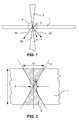
figure 1 schematically shows a beam impinging on a sample, -
figure 2 schematically shows a detail fromfigure 1 , -
figure 3 shows a schematic curve of resolution as a function of opening half-angle, -
figure 4 shows a schematic curve showing resolution R(α) and diameter D for different sample thicknesses versus opening half-angle, and -
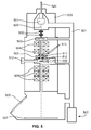
figure 5 schematically shows a STEM. -
Figure 1 schematically shows a beam impinging on a sample. Asample 1 is illuminated with afocused beam 2. The focused beam forms across-over 3 in the sample. Part of the electrons forming thebeam 1 are transmitted through the sample and exit the sample. The electrons transmitted through the sample are bothunscattered electrons 4, which are not deflected, andscattered electrons figure 2 -
Figure 2 schematically shows a detail offigure 1 . It shows an enlarged view of area A offigure 1 . The scatteredelectrons figure 1 are omitted for clarity, although such electrons are still generated. Theimpinging beam 2 irradiates the volume 6 of thesample 1. The beam has a cross-over with a diameter R, said diameter being a function of the opening half-angle α ofbeam 1. - Disregarding the contribution of aberrations, the beam has at the surface of the sample a diameter D due to the opening half-angle α. This diameter D is a function of the opening half-angle α, and the thickness T of the sample. In the optimum situation, where the cross-over is in the middle of the sample, D = T tan(α).
- As mentioned before, the optimum cross-over diameter obtainable with commercial microscopes is nowadays approximately 0.1 nm. This is achieved with an opening half-angle α of between 5 and 15 mrad, and very thin samples. Using a sample with a thickness T of e.g. 1 µm, and an opening half-angle of 10 mrad, the diameter D would be approximately 10 nm. This shows that such extreme resolution can only be achieved for extremely thin samples.
- It is noted that when using a beam in which part of the beam has a small diameter and a part of the beam has a large diameter, a high resolution can be achieved for those parts of the sample at the cross-over plane. However, from other parts of the sample (removed from the cross-over plane) only blurred information can be derived.
-
Figure 3 shows a schematic curve of resolution as a function of opening half-angle. The curve is representative for a 300 kV microscope having a spherical aberration of 1.2 mm and negligible chromatic aberration and negligible source size. Therefore only spherical aberration and diffraction contribute to the diameter of the cross-over. For this instrument the optimum cross-over diameter R(α) is approximately 0.15 nm at an opening half-angle α of 8 mrad.
It is noted that several methods may be used to add the different contributions. Here the method described in "Addition of different contributions to the charged-particle beam size", J.E. Barth et al, Optik 1996 (101), pages 101-109 is used.
It is remarked that here the diameter of the spherical aberration and the diameter of the diffraction are used to add up to the diameter of the cross-over R(α). -
Figure 4 shows a schematic curve showing resolution R(α) and diameter D for different sample thicknesses versus opening half-angle. In this figure the same curve for the diameter of the cross-over R(α) is shown. Also shown are curves for different sample thicknesses T representing the diameter D at the surface of the sample resulting from the opening angle used. As can be seen clearly, at an opening angle of 8 mrad, corresponding with the optimum cross-over diameter, the diameter D for a 100 nm thick sample is 0.8 nm, much larger than the diameter of the cross-over. For a sample with a thickness of 250 nm the diameter of the cross-over is 2 nm, and for a 500 nm thick sample even 4 nm. - At positions X1 ... X5 the cross-over diameter R(α) is approximately equal to the diameter D, and therefore a balance between the contributions due to cross-over diameter and convergence angle occurs at the corresponding opening half-angles. For a 100 nm thick sample the maximum diameter of the beam is now approximately 0.4 nm, a factor two lower than when using the opening half-angle giving the optimum cross-over diameter. For a sample with a thickness of e.g. 500 nm the maximum diameter is now only approximately 0.8 nm instead of 4 nm, an improvement of approximately 5 times when compared to the maximum beam diameter at 8 mrad, although 5 times worse than the cross-over diameter of 0.15 nm at 8 mrad, i.e. the resolution that can be achieved for very thin samples..
- It is noted that the optimum opening half-angle can be computed, but that a look-up table can be used as well to determine the optimum opening half-angle.
- It is further noted that, although the curve for the cross-over diameter and the curves for the thicknesses may show two intersections, the minimum diameter always occurs for an opening half-angle equal to or less than the opening half-angle resulting in optimum cross-over diameter.
-
Figure 5 schematically shows a STEM. - In
figure 5 aparticle source 501 produces a beam of electrons travelling round particle-optical axis 500. The particle source is fed viahigh voltage wire 524 to electronics (not shown), the electronics delivering appropriate voltage and current for the operation of the particle source. The beam of electrons is centred round particle-optical axis by e.g. particle-optical deflectors 502.Diaphragm 503 shows an aperture acting as a beam limiting aperture. Particle-optical lenses 502 act as a condenser for delivering the beam of electrons to theobjective lens 505. A sample mounted onsample holder 511 is illuminated by the particle beam, and a fraction of the electrons pass through the specimen. These electrons are imaged by particle-optical lenses 506 onto adetector 507.Detector 507 can be e.g. a fluorescent screen or a CCD camera. When a fluorescent screen is used, the image may be viewed throughglass window 508.
The beam is scanned over the surface of the sample by particle-optical deflector 510. The interior of the microscope is enveloped by avacuum wall 520, and evacuated byvacuum pump 522 viavacuum connections 521.
For positioning the specimen holder amanipulator 509 is used. Anairlock 512 enables the introduction of a specimen mounted on a specimen holder into the evacuated interior of the TEM and the mounting of the specimen holder onto the sub-stage. - The opening angle of the beam impinging on the sample is set by the focal length of the objective lens 505 (which for a given instrument is a largely fixed value), the magnification of the
condenser lenses 504 and the size of the aperture indiaphragm 503. - It is noted that, as known to the person skilled in the art, many models of STEMs are known, with different number of lenses, deflectors, different manipulators, detectors, etc..
Claims (15)
- Method for obtaining a transmission image of a sample (1) in a particle-optical apparatus, said apparatus equipped to image a sample by scanning the sample with a finely focused beam of particles (2) and detecting particles transmitted through the sample (4, 5A, 5B, 5C), said finely focused beam showing a smallest diameter (3), the so-named cross-over, the diameter of the cross-over R being a function of the opening half-angle α of the finely focused beam, the method comprising:• acquiring an image of the sample (1) by scanning the sample with the finely focused beam of particles (2) and detecting particles transmitted through the sample (4, 5A, 5B, 5C),characterized in that, before the image is acquired,• the thickness T of the sample is determined or estimated,• the length L of the sample material through which the transmitted particles have to travel is derived from the thickness T of the sample, and• the opening half-angle α is set to a value such that 0.5 · R(α) / L ≤ tan(α) ≤ 2 · R(α) / L, as a result of which the sample is scanned with a beam having a substantially constant diameter over a length equal to the length L of the sample material through which the transmitted particles have to travel.
- The method according to claim 1 in which the sample (1) is substantially perpendicular to the finely focused beam (2) and the length L of the sample material through which the transmitted particles (4, 5A, 5B, 5C) have to travel substantially equals the thickness T of the sample, and the opening half-angle α of the finely focused beam is set to a value α such that 0.5 · R(α) / T ≤ tan(α ) ≤ 2 · R(α) / T .
- The method according to claim 1 in which a line normal to the surface to the sample (1) is tilted over an angle β with respect to the finely focused beam (2) before the image is acquired, as a result of which the length L of the sample material through which the transmitted particles (4, 5A, 5B, 5C) have to travel equals the thickness T of the sample multiplied by the cosine of the tilt angle β, and the opening half-angle α of the finely focused beam is set to a value α such that 0.5 · R(α) · cos (β)/T ≤ tan(α ) ≤ 2 · R(α) · cos (β) / T.
- The method according to claim 1 in which, the method further comprising forming a 3D reconstruction by:• determining a maximum tilt angle βmax and a number of images to be acquired,• determining the maximum length Lmax of the sample material through which the transmitted particles have to travel, Lmax = T / cos (βmax)• setting the opening half-angle α of the finely focused beam (2) to a value α such that 0.5 · R(α) · cos (βmax) / T ≤ tan(α ) ≤ 2 · R(α) · cos (βmax) / T,• acquiring a series of images at different tilt angles, each of the different tilt angles being equal to or less than the maximum tilt angle βmax, and• combining said series of images in a 3D reconstruction of the bulk information of the sample (1).
- The method according to any of the preceding claims in which the sample (1) shows two substantially flat surfaces and the cross-over is located between said surfaces.
- The method according to claim 5 in which the cross-over is located substantially halfway the two surfaces.
- The method according to any of claims 3-6 in which the focal length of the lens focusing the finely focused beam (2) is changed during the scanning of the finely focused beam over the sample (1) so as to compensate for the tilting of the sample relative to the beam, thereby keeping the distance of the cross-over with respect to a surface of the sample substantially constant.
- The method according to any of the preceding claims in which the thickness T of the sample is larger than 100 nm.
- The method according to claim 8 in which the thickness T of the sample is larger than 1000 nm.
- The method according to any of the preceding claims in which the apparatus is a scanning transmission electron microscope.
- The method according to any of the preceding claims in which the sample (1) is an amorphous sample.
- Software for programming a programmable controller of a particle-optical apparatus, the apparatus equipped to scan a finely focused beam of particles (2) over a sample (1) and to detect particles (4, 5A, 5B, 5C) transmitted through the sample, the controller equipped to control the opening half-angle α of the finely focused beam and the focal plane of the finely focused beam, characterized in that the software comprises code for programming the controller to adjust the opening half-angle α of the finely focused beam as a function of a variable representing the thickness T of the sample.
- The software according to claim 12 in which the software further comprises code for programming the controller to obtain the variable representing the thickness T of the sample (1) via a user interface of the particle-optical apparatus.
- The software according to claim 12 or claim 13 in which the software further comprises code for programming the controller to adjust the opening half-angle α of the finely focused beam (2) as a function of a variable representing the tilt β of the sample (1) with respect to the finely focused beam.
- The software according to claim 14 in which the software further comprises code for programming the controller to adjust the focal plane of the finely focused beam as a function of the variable representing the tilt β of the sample (1) with respect to the finely focused beam (2), resulting in a focal plane that is tilted with respect to the finely focused beam.
Priority Applications (1)
| Application Number | Priority Date | Filing Date | Title |
|---|---|---|---|
| EP08169468A EP2063449B1 (en) | 2007-11-21 | 2008-11-20 | Method for obtaining a scanning transmission image of a sample in a particle-optical apparatus |
Applications Claiming Priority (2)
| Application Number | Priority Date | Filing Date | Title |
|---|---|---|---|
| EP07121186A EP2063450A1 (en) | 2007-11-21 | 2007-11-21 | Method for obtaining a scanning transmission image of a sample in a particle-optical apparatus |
| EP08169468A EP2063449B1 (en) | 2007-11-21 | 2008-11-20 | Method for obtaining a scanning transmission image of a sample in a particle-optical apparatus |
Publications (2)
| Publication Number | Publication Date |
|---|---|
| EP2063449A1 true EP2063449A1 (en) | 2009-05-27 |
| EP2063449B1 EP2063449B1 (en) | 2011-04-13 |
Family
ID=39278317
Family Applications (2)
| Application Number | Title | Priority Date | Filing Date |
|---|---|---|---|
| EP07121186A Withdrawn EP2063450A1 (en) | 2007-11-21 | 2007-11-21 | Method for obtaining a scanning transmission image of a sample in a particle-optical apparatus |
| EP08169468A Active EP2063449B1 (en) | 2007-11-21 | 2008-11-20 | Method for obtaining a scanning transmission image of a sample in a particle-optical apparatus |
Family Applications Before (1)
| Application Number | Title | Priority Date | Filing Date |
|---|---|---|---|
| EP07121186A Withdrawn EP2063450A1 (en) | 2007-11-21 | 2007-11-21 | Method for obtaining a scanning transmission image of a sample in a particle-optical apparatus |
Country Status (6)
| Country | Link |
|---|---|
| US (1) | US7825378B2 (en) |
| EP (2) | EP2063450A1 (en) |
| JP (1) | JP5404008B2 (en) |
| CN (1) | CN101499398B (en) |
| AT (1) | ATE505808T1 (en) |
| DE (1) | DE602008006152D1 (en) |
Cited By (2)
| Publication number | Priority date | Publication date | Assignee | Title |
|---|---|---|---|---|
| EP2562534A3 (en) * | 2011-08-23 | 2014-05-21 | Sumitomo Rubber Industries, Ltd. | Method for analyzing rubber compound with filler particles |
| EP2738787A1 (en) * | 2012-11-29 | 2014-06-04 | Fei Company | Method of performing tomographic imaging of a sample in a charged-particle microscope |
Families Citing this family (19)
| Publication number | Priority date | Publication date | Assignee | Title |
|---|---|---|---|---|
| US8080791B2 (en) | 2008-12-12 | 2011-12-20 | Fei Company | X-ray detector for electron microscope |
| EP2388796A1 (en) | 2010-05-21 | 2011-11-23 | FEI Company | Simultaneous electron detection |
| CN102971824B (en) * | 2010-07-14 | 2016-01-13 | Fei公司 | For the improvement contrast of scanning confocal electron microscope |
| JP5423612B2 (en) * | 2010-08-16 | 2014-02-19 | 富士通株式会社 | Confocal scanning transmission electron microscope apparatus and three-dimensional tomographic image observation method |
| JP5767477B2 (en) * | 2011-01-14 | 2015-08-19 | 住友ゴム工業株式会社 | How to observe rubber materials |
| JP2013044607A (en) * | 2011-08-23 | 2013-03-04 | Sumitomo Rubber Ind Ltd | Method of observing rubber material |
| JP2013057638A (en) * | 2011-09-09 | 2013-03-28 | Sumitomo Rubber Ind Ltd | Simulation method for rubber materials |
| JP5993218B2 (en) * | 2012-06-04 | 2016-09-14 | 住友ゴム工業株式会社 | How to observe rubber materials |
| EP2708874A1 (en) | 2012-09-12 | 2014-03-19 | Fei Company | Method of performing tomographic imaging of a sample in a charged-particle microscope |
| EP3102966A4 (en) | 2014-02-03 | 2017-10-11 | The Arizona Board of Regents On Behalf of the University of Arizona | Beta and alpha emission tomography for three-dimensional autoradiography |
| EP2911180A1 (en) * | 2014-02-24 | 2015-08-26 | FEI Company | Method of examining a sample in a charged-particle microscope |
| US10170274B2 (en) * | 2015-03-18 | 2019-01-01 | Battelle Memorial Institute | TEM phase contrast imaging with image plane phase grating |
| US10109453B2 (en) | 2015-03-18 | 2018-10-23 | Battelle Memorial Institute | Electron beam masks for compressive sensors |
| US10580614B2 (en) | 2016-04-29 | 2020-03-03 | Battelle Memorial Institute | Compressive scanning spectroscopy |
| US10295677B2 (en) | 2017-05-08 | 2019-05-21 | Battelle Memorial Institute | Systems and methods for data storage and retrieval |
| US11141064B2 (en) * | 2017-07-19 | 2021-10-12 | Perkinelmer Health Sciences, Inc. | Systems and methods for rapid wide field illumination scanning for in vivo small animal fluorescence tomographic imaging |
| US11153499B2 (en) | 2017-07-19 | 2021-10-19 | Perkinelmer Health Sciences, Inc. | Rapid, high dynamic range image acquisition with a charge-coupled device (CCD) camera |
| US10453646B2 (en) * | 2017-09-06 | 2019-10-22 | Fei Company | Tomography-assisted TEM prep with requested intervention automation workflow |
| JP6995103B2 (en) * | 2019-11-15 | 2022-01-14 | 日本電子株式会社 | Control method of transmission electron microscope and transmission electron microscope |
Family Cites Families (6)
| Publication number | Priority date | Publication date | Assignee | Title |
|---|---|---|---|---|
| WO2001054163A1 (en) * | 2000-01-21 | 2001-07-26 | Koninklijke Philips Electronics N.V. | Shaped and low density focused ion beams |
| US6946654B2 (en) * | 2000-04-24 | 2005-09-20 | Fei Company | Collection of secondary electrons through the objective lens of a scanning electron microscope |
| US6977386B2 (en) * | 2001-01-19 | 2005-12-20 | Fei Company | Angular aperture shaped beam system and method |
| JP2003249186A (en) * | 2002-02-22 | 2003-09-05 | Fujitsu Ltd | Observation method and observation apparatus using scanning transmission electron microscope |
| JP2004199884A (en) * | 2002-12-16 | 2004-07-15 | Sony Corp | Electron diffraction device |
| NL1029066C2 (en) * | 2005-04-05 | 2006-10-09 | Fei Co | Aberration corrector for e.g. transmission electron microscope or scanning electron microscope, has first and second octupoles not imaged upon one another, and second and third octupoles imaged upon one another, in first axial plane |
-
2007
- 2007-11-21 EP EP07121186A patent/EP2063450A1/en not_active Withdrawn
-
2008
- 2008-11-20 EP EP08169468A patent/EP2063449B1/en active Active
- 2008-11-20 DE DE602008006152T patent/DE602008006152D1/en active Active
- 2008-11-20 JP JP2008296424A patent/JP5404008B2/en active Active
- 2008-11-20 AT AT08169468T patent/ATE505808T1/en not_active IP Right Cessation
- 2008-11-20 US US12/274,962 patent/US7825378B2/en active Active
- 2008-11-21 CN CN2008101818977A patent/CN101499398B/en active Active
Non-Patent Citations (7)
| Title |
|---|
| BENDER H ET AL: "3D-analysis of semiconductor structures by electron tomography", MICROELECTRONIC ENGINEERING ELSEVIER SCIENCE B.V. NETHERLANDS, vol. 84, no. 11, 26 May 2007 (2007-05-26), pages 2707 - 2713, XP002482365, ISSN: 0167-9317 * |
| BORISEVICH A Y ET AL: "Depth sectioning with the aberration-corrected scanning transmission electron microscope", PROCEEDINGS OF THE NATIONAL ACADEMY OF SCIENCES OF THE UNITED STATES OF AMERICA NATIONAL ACADEMY OF SCIENCES OF THE UNITED STATES OF AMERICA USA, vol. 103, no. 9, 28 February 2006 (2006-02-28), pages 3044 - 3048, XP002482369, ISSN: 0027-8424 * |
| C. KUBEL ET AL.: "Recent advances in Electron Tomography: TEM and HAADF-STEM Tomography for materials science and IC applications", MICROSCOPY AND MICROANALYSIS, vol. 11, no. 5, 2005, pages 378 - 400, XP009099036 |
| J.E. BARTH ET AL.: "Addition of different contributions to the charged-particle beam size", OPTIK, vol. 101, 1996, pages 101 - 109 |
| KUBEL C ET AL: "Recent advances in electron tomography: TEM and HAADF-STEM tomography for materials science and semiconductor applications", MICROSCOPY AND MICROANALYSIS, SPRINGER, NEW YORK, NY, US, vol. 11, no. 5, 1 October 2005 (2005-10-01), pages 378 - 400, XP009099036, ISSN: 1431-9276 * |
| L. REIMER: "Transmission Electron Microscopy", SPRINGER VERLAG |
| TREACY M M J ET AL: "Atomic contrast transfer in annular darkfield images", JOURNAL OF MICROSCOPY, OXFORD, vol. 180, 1 October 1995 (1995-10-01), pages 2 - 11, XP009100840, ISSN: 0022-2720 * |
Cited By (3)
| Publication number | Priority date | Publication date | Assignee | Title |
|---|---|---|---|---|
| EP2562534A3 (en) * | 2011-08-23 | 2014-05-21 | Sumitomo Rubber Industries, Ltd. | Method for analyzing rubber compound with filler particles |
| EP2738787A1 (en) * | 2012-11-29 | 2014-06-04 | Fei Company | Method of performing tomographic imaging of a sample in a charged-particle microscope |
| EP2738786A1 (en) * | 2012-11-29 | 2014-06-04 | Fei Company | Method of performing tomographic imaging of a sample in a charged-particle microscope |
Also Published As
| Publication number | Publication date |
|---|---|
| EP2063450A1 (en) | 2009-05-27 |
| CN101499398A (en) | 2009-08-05 |
| JP5404008B2 (en) | 2014-01-29 |
| ATE505808T1 (en) | 2011-04-15 |
| CN101499398B (en) | 2012-06-27 |
| JP2009129909A (en) | 2009-06-11 |
| US7825378B2 (en) | 2010-11-02 |
| DE602008006152D1 (en) | 2011-05-26 |
| US20090133167A1 (en) | 2009-05-21 |
| EP2063449B1 (en) | 2011-04-13 |
Similar Documents
| Publication | Publication Date | Title |
|---|---|---|
| US7825378B2 (en) | Method for obtaining a scanning transmission image of a sample in a particle-optical apparatus | |
| US7223983B2 (en) | Charged particle beam column | |
| EP2320217B1 (en) | SACP method and particle optical system for performing the method | |
| US10103002B1 (en) | Method for generating an image of an object and particle beam device for carrying out the method | |
| EP2091062A1 (en) | TEM with aberration corrector and phase plate | |
| EP2511936B1 (en) | Distortion free stigmation of a TEM | |
| CN108538693B (en) | Aberration measurement of charged particle microscope | |
| EP2477206B1 (en) | Method for processing and/or analyzing a sample with a particle beam device | |
| EP2738786A1 (en) | Method of performing tomographic imaging of a sample in a charged-particle microscope | |
| CN108140525B (en) | Scanning transmission electron microscope with electron energy loss spectrometer and observation method thereof | |
| JP2008181786A (en) | Charged particle beam equipment | |
| Goldstein et al. | The SEM and its modes of operation | |
| US8884245B2 (en) | Corrector for the correction of chromatic aberrations in a particle-optical apparatus | |
| Cheney | Introduction to scanning electron microscopy | |
| CN112309812B (en) | Method for operating a particle beam microscope and particle beam microscope | |
| JP4668807B2 (en) | Charged particle beam apparatus and charged particle beam image generation method | |
| JP7736589B2 (en) | Measurement method and electron microscope | |
| US12476072B2 (en) | Operating a particle beam apparatus | |
| JP2010102938A (en) | Charged particle beam apparatus and focused ion beam apparatus | |
| Stefanaki | Electron microscopy: the basics | |
| Gajghate | Introduction to Microscopy | |
| JP3814968B2 (en) | Inspection device | |
| JP2008052935A (en) | Scanning electron microscope | |
| Daniel et al. | Scanning Electron Microscopy as a Powerful Morphological Characterization Technique for Polymer Blends and Polymer Nanocomposites | |
| WO2010125347A2 (en) | Inelastic scanning confocal electron microscopy |
Legal Events
| Date | Code | Title | Description |
|---|---|---|---|
| PUAI | Public reference made under article 153(3) epc to a published international application that has entered the european phase |
Free format text: ORIGINAL CODE: 0009012 |
|
| AK | Designated contracting states |
Kind code of ref document: A1 Designated state(s): AT BE BG CH CY CZ DE DK EE ES FI FR GB GR HR HU IE IS IT LI LT LU LV MC MT NL NO PL PT RO SE SI SK TR |
|
| AX | Request for extension of the european patent |
Extension state: AL BA MK RS |
|
| 17P | Request for examination filed |
Effective date: 20090605 |
|
| 17Q | First examination report despatched |
Effective date: 20090703 |
|
| AKX | Designation fees paid |
Designated state(s): AT BE BG CH CY CZ DE DK EE ES FI FR GB GR HR HU IE IS IT LI LT LU LV MC MT NL NO PL PT RO SE SI SK TR |
|
| GRAP | Despatch of communication of intention to grant a patent |
Free format text: ORIGINAL CODE: EPIDOSNIGR1 |
|
| GRAS | Grant fee paid |
Free format text: ORIGINAL CODE: EPIDOSNIGR3 |
|
| GRAA | (expected) grant |
Free format text: ORIGINAL CODE: 0009210 |
|
| AK | Designated contracting states |
Kind code of ref document: B1 Designated state(s): AT BE BG CH CY CZ DE DK EE ES FI FR GB GR HR HU IE IS IT LI LT LU LV MC MT NL NO PL PT RO SE SI SK TR |
|
| REG | Reference to a national code |
Ref country code: GB Ref legal event code: FG4D |
|
| REG | Reference to a national code |
Ref country code: CH Ref legal event code: EP |
|
| REG | Reference to a national code |
Ref country code: IE Ref legal event code: FG4D |
|
| REF | Corresponds to: |
Ref document number: 602008006152 Country of ref document: DE Date of ref document: 20110526 Kind code of ref document: P |
|
| REG | Reference to a national code |
Ref country code: DE Ref legal event code: R096 Ref document number: 602008006152 Country of ref document: DE Effective date: 20110526 |
|
| REG | Reference to a national code |
Ref country code: NL Ref legal event code: VDEP Effective date: 20110413 |
|
| LTIE | Lt: invalidation of european patent or patent extension |
Effective date: 20110413 |
|
| PG25 | Lapsed in a contracting state [announced via postgrant information from national office to epo] |
Ref country code: SE Free format text: LAPSE BECAUSE OF FAILURE TO SUBMIT A TRANSLATION OF THE DESCRIPTION OR TO PAY THE FEE WITHIN THE PRESCRIBED TIME-LIMIT Effective date: 20110413 Ref country code: HR Free format text: LAPSE BECAUSE OF FAILURE TO SUBMIT A TRANSLATION OF THE DESCRIPTION OR TO PAY THE FEE WITHIN THE PRESCRIBED TIME-LIMIT Effective date: 20110413 Ref country code: NO Free format text: LAPSE BECAUSE OF FAILURE TO SUBMIT A TRANSLATION OF THE DESCRIPTION OR TO PAY THE FEE WITHIN THE PRESCRIBED TIME-LIMIT Effective date: 20110713 Ref country code: PT Free format text: LAPSE BECAUSE OF FAILURE TO SUBMIT A TRANSLATION OF THE DESCRIPTION OR TO PAY THE FEE WITHIN THE PRESCRIBED TIME-LIMIT Effective date: 20110816 Ref country code: LT Free format text: LAPSE BECAUSE OF FAILURE TO SUBMIT A TRANSLATION OF THE DESCRIPTION OR TO PAY THE FEE WITHIN THE PRESCRIBED TIME-LIMIT Effective date: 20110413 |
|
| PG25 | Lapsed in a contracting state [announced via postgrant information from national office to epo] |
Ref country code: FI Free format text: LAPSE BECAUSE OF FAILURE TO SUBMIT A TRANSLATION OF THE DESCRIPTION OR TO PAY THE FEE WITHIN THE PRESCRIBED TIME-LIMIT Effective date: 20110413 Ref country code: GR Free format text: LAPSE BECAUSE OF FAILURE TO SUBMIT A TRANSLATION OF THE DESCRIPTION OR TO PAY THE FEE WITHIN THE PRESCRIBED TIME-LIMIT Effective date: 20110714 Ref country code: LV Free format text: LAPSE BECAUSE OF FAILURE TO SUBMIT A TRANSLATION OF THE DESCRIPTION OR TO PAY THE FEE WITHIN THE PRESCRIBED TIME-LIMIT Effective date: 20110413 Ref country code: BE Free format text: LAPSE BECAUSE OF FAILURE TO SUBMIT A TRANSLATION OF THE DESCRIPTION OR TO PAY THE FEE WITHIN THE PRESCRIBED TIME-LIMIT Effective date: 20110413 Ref country code: AT Free format text: LAPSE BECAUSE OF FAILURE TO SUBMIT A TRANSLATION OF THE DESCRIPTION OR TO PAY THE FEE WITHIN THE PRESCRIBED TIME-LIMIT Effective date: 20110413 Ref country code: IS Free format text: LAPSE BECAUSE OF FAILURE TO SUBMIT A TRANSLATION OF THE DESCRIPTION OR TO PAY THE FEE WITHIN THE PRESCRIBED TIME-LIMIT Effective date: 20110813 Ref country code: CY Free format text: LAPSE BECAUSE OF FAILURE TO SUBMIT A TRANSLATION OF THE DESCRIPTION OR TO PAY THE FEE WITHIN THE PRESCRIBED TIME-LIMIT Effective date: 20110413 Ref country code: ES Free format text: LAPSE BECAUSE OF FAILURE TO SUBMIT A TRANSLATION OF THE DESCRIPTION OR TO PAY THE FEE WITHIN THE PRESCRIBED TIME-LIMIT Effective date: 20110724 Ref country code: SI Free format text: LAPSE BECAUSE OF FAILURE TO SUBMIT A TRANSLATION OF THE DESCRIPTION OR TO PAY THE FEE WITHIN THE PRESCRIBED TIME-LIMIT Effective date: 20110413 |
|
| PG25 | Lapsed in a contracting state [announced via postgrant information from national office to epo] |
Ref country code: NL Free format text: LAPSE BECAUSE OF FAILURE TO SUBMIT A TRANSLATION OF THE DESCRIPTION OR TO PAY THE FEE WITHIN THE PRESCRIBED TIME-LIMIT Effective date: 20110413 |
|
| PG25 | Lapsed in a contracting state [announced via postgrant information from national office to epo] |
Ref country code: EE Free format text: LAPSE BECAUSE OF FAILURE TO SUBMIT A TRANSLATION OF THE DESCRIPTION OR TO PAY THE FEE WITHIN THE PRESCRIBED TIME-LIMIT Effective date: 20110413 Ref country code: CZ Free format text: LAPSE BECAUSE OF FAILURE TO SUBMIT A TRANSLATION OF THE DESCRIPTION OR TO PAY THE FEE WITHIN THE PRESCRIBED TIME-LIMIT Effective date: 20110413 |
|
| PLBE | No opposition filed within time limit |
Free format text: ORIGINAL CODE: 0009261 |
|
| STAA | Information on the status of an ep patent application or granted ep patent |
Free format text: STATUS: NO OPPOSITION FILED WITHIN TIME LIMIT |
|
| PG25 | Lapsed in a contracting state [announced via postgrant information from national office to epo] |
Ref country code: DK Free format text: LAPSE BECAUSE OF FAILURE TO SUBMIT A TRANSLATION OF THE DESCRIPTION OR TO PAY THE FEE WITHIN THE PRESCRIBED TIME-LIMIT Effective date: 20110413 Ref country code: PL Free format text: LAPSE BECAUSE OF FAILURE TO SUBMIT A TRANSLATION OF THE DESCRIPTION OR TO PAY THE FEE WITHIN THE PRESCRIBED TIME-LIMIT Effective date: 20110413 Ref country code: RO Free format text: LAPSE BECAUSE OF FAILURE TO SUBMIT A TRANSLATION OF THE DESCRIPTION OR TO PAY THE FEE WITHIN THE PRESCRIBED TIME-LIMIT Effective date: 20110413 Ref country code: SK Free format text: LAPSE BECAUSE OF FAILURE TO SUBMIT A TRANSLATION OF THE DESCRIPTION OR TO PAY THE FEE WITHIN THE PRESCRIBED TIME-LIMIT Effective date: 20110413 |
|
| 26N | No opposition filed |
Effective date: 20120116 |
|
| REG | Reference to a national code |
Ref country code: DE Ref legal event code: R097 Ref document number: 602008006152 Country of ref document: DE Effective date: 20120116 |
|
| PG25 | Lapsed in a contracting state [announced via postgrant information from national office to epo] |
Ref country code: IT Free format text: LAPSE BECAUSE OF FAILURE TO SUBMIT A TRANSLATION OF THE DESCRIPTION OR TO PAY THE FEE WITHIN THE PRESCRIBED TIME-LIMIT Effective date: 20110413 |
|
| PG25 | Lapsed in a contracting state [announced via postgrant information from national office to epo] |
Ref country code: MC Free format text: LAPSE BECAUSE OF NON-PAYMENT OF DUE FEES Effective date: 20111130 |
|
| REG | Reference to a national code |
Ref country code: IE Ref legal event code: MM4A |
|
| PG25 | Lapsed in a contracting state [announced via postgrant information from national office to epo] |
Ref country code: IE Free format text: LAPSE BECAUSE OF NON-PAYMENT OF DUE FEES Effective date: 20111120 |
|
| PG25 | Lapsed in a contracting state [announced via postgrant information from national office to epo] |
Ref country code: MT Free format text: LAPSE BECAUSE OF FAILURE TO SUBMIT A TRANSLATION OF THE DESCRIPTION OR TO PAY THE FEE WITHIN THE PRESCRIBED TIME-LIMIT Effective date: 20110413 |
|
| PG25 | Lapsed in a contracting state [announced via postgrant information from national office to epo] |
Ref country code: LU Free format text: LAPSE BECAUSE OF NON-PAYMENT OF DUE FEES Effective date: 20111120 |
|
| PG25 | Lapsed in a contracting state [announced via postgrant information from national office to epo] |
Ref country code: BG Free format text: LAPSE BECAUSE OF FAILURE TO SUBMIT A TRANSLATION OF THE DESCRIPTION OR TO PAY THE FEE WITHIN THE PRESCRIBED TIME-LIMIT Effective date: 20110713 |
|
| REG | Reference to a national code |
Ref country code: CH Ref legal event code: PL |
|
| PG25 | Lapsed in a contracting state [announced via postgrant information from national office to epo] |
Ref country code: CH Free format text: LAPSE BECAUSE OF NON-PAYMENT OF DUE FEES Effective date: 20121130 Ref country code: LI Free format text: LAPSE BECAUSE OF NON-PAYMENT OF DUE FEES Effective date: 20121130 |
|
| PG25 | Lapsed in a contracting state [announced via postgrant information from national office to epo] |
Ref country code: TR Free format text: LAPSE BECAUSE OF FAILURE TO SUBMIT A TRANSLATION OF THE DESCRIPTION OR TO PAY THE FEE WITHIN THE PRESCRIBED TIME-LIMIT Effective date: 20110413 |
|
| PG25 | Lapsed in a contracting state [announced via postgrant information from national office to epo] |
Ref country code: HU Free format text: LAPSE BECAUSE OF FAILURE TO SUBMIT A TRANSLATION OF THE DESCRIPTION OR TO PAY THE FEE WITHIN THE PRESCRIBED TIME-LIMIT Effective date: 20110413 |
|
| REG | Reference to a national code |
Ref country code: FR Ref legal event code: PLFP Year of fee payment: 8 |
|
| REG | Reference to a national code |
Ref country code: FR Ref legal event code: PLFP Year of fee payment: 9 |
|
| REG | Reference to a national code |
Ref country code: FR Ref legal event code: PLFP Year of fee payment: 10 |
|
| REG | Reference to a national code |
Ref country code: FR Ref legal event code: PLFP Year of fee payment: 11 |
|
| PGFP | Annual fee paid to national office [announced via postgrant information from national office to epo] |
Ref country code: DE Payment date: 20251010 Year of fee payment: 18 |
|
| PGFP | Annual fee paid to national office [announced via postgrant information from national office to epo] |
Ref country code: GB Payment date: 20251114 Year of fee payment: 18 |
|
| PGFP | Annual fee paid to national office [announced via postgrant information from national office to epo] |
Ref country code: FR Payment date: 20251111 Year of fee payment: 18 |