EP2058871A1 - Photodetector and method for manufacturing photodetector - Google Patents
Photodetector and method for manufacturing photodetector Download PDFInfo
- Publication number
- EP2058871A1 EP2058871A1 EP07793014A EP07793014A EP2058871A1 EP 2058871 A1 EP2058871 A1 EP 2058871A1 EP 07793014 A EP07793014 A EP 07793014A EP 07793014 A EP07793014 A EP 07793014A EP 2058871 A1 EP2058871 A1 EP 2058871A1
- Authority
- EP
- European Patent Office
- Prior art keywords
- conductivity
- layer
- type
- insulating film
- inorganic insulating
- Prior art date
- Legal status (The legal status is an assumption and is not a legal conclusion. Google has not performed a legal analysis and makes no representation as to the accuracy of the status listed.)
- Withdrawn
Links
- 238000004519 manufacturing process Methods 0.000 title claims description 17
- 238000000034 method Methods 0.000 title 1
- 239000012535 impurity Substances 0.000 claims abstract description 102
- 229910000673 Indium arsenide Inorganic materials 0.000 claims abstract description 78
- RPQDHPTXJYYUPQ-UHFFFAOYSA-N indium arsenide Chemical compound [In]#[As] RPQDHPTXJYYUPQ-UHFFFAOYSA-N 0.000 claims abstract description 78
- 239000004065 semiconductor Substances 0.000 claims abstract description 73
- 239000000758 substrate Substances 0.000 claims abstract description 23
- 230000008021 deposition Effects 0.000 claims abstract description 22
- 238000000151 deposition Methods 0.000 claims description 29
- 229910052785 arsenic Inorganic materials 0.000 claims description 11
- 238000009792 diffusion process Methods 0.000 claims description 8
- 229910052738 indium Inorganic materials 0.000 claims description 8
- 238000005468 ion implantation Methods 0.000 claims description 5
- 238000009826 distribution Methods 0.000 claims description 3
- 239000000463 material Substances 0.000 description 16
- 239000013078 crystal Substances 0.000 description 8
- 230000031700 light absorption Effects 0.000 description 6
- 238000010521 absorption reaction Methods 0.000 description 5
- 230000035945 sensitivity Effects 0.000 description 5
- 229910052793 cadmium Inorganic materials 0.000 description 4
- 238000000206 photolithography Methods 0.000 description 4
- 229910052725 zinc Inorganic materials 0.000 description 4
- VYPSYNLAJGMNEJ-UHFFFAOYSA-N Silicium dioxide Chemical compound O=[Si]=O VYPSYNLAJGMNEJ-UHFFFAOYSA-N 0.000 description 3
- 238000005229 chemical vapour deposition Methods 0.000 description 3
- 238000005530 etching Methods 0.000 description 3
- 239000000969 carrier Substances 0.000 description 2
- 229910052737 gold Inorganic materials 0.000 description 2
- 238000010438 heat treatment Methods 0.000 description 2
- 238000004943 liquid phase epitaxy Methods 0.000 description 2
- 238000005259 measurement Methods 0.000 description 2
- 238000000927 vapour-phase epitaxy Methods 0.000 description 2
- 229910052581 Si3N4 Inorganic materials 0.000 description 1
- 238000000137 annealing Methods 0.000 description 1
- 230000015572 biosynthetic process Effects 0.000 description 1
- 229910052681 coesite Inorganic materials 0.000 description 1
- 150000001875 compounds Chemical class 0.000 description 1
- 229910052906 cristobalite Inorganic materials 0.000 description 1
- 230000003247 decreasing effect Effects 0.000 description 1
- 230000000694 effects Effects 0.000 description 1
- -1 for example Substances 0.000 description 1
- 238000002513 implantation Methods 0.000 description 1
- 150000002500 ions Chemical class 0.000 description 1
- 238000012986 modification Methods 0.000 description 1
- 230000004048 modification Effects 0.000 description 1
- 238000001451 molecular beam epitaxy Methods 0.000 description 1
- 239000010453 quartz Substances 0.000 description 1
- 239000000377 silicon dioxide Substances 0.000 description 1
- 229910052682 stishovite Inorganic materials 0.000 description 1
- 230000002123 temporal effect Effects 0.000 description 1
- 229910052905 tridymite Inorganic materials 0.000 description 1
Images




Classifications
-
- H—ELECTRICITY
- H10—SEMICONDUCTOR DEVICES; ELECTRIC SOLID-STATE DEVICES NOT OTHERWISE PROVIDED FOR
- H10F—INORGANIC SEMICONDUCTOR DEVICES SENSITIVE TO INFRARED RADIATION, LIGHT, ELECTROMAGNETIC RADIATION OF SHORTER WAVELENGTH OR CORPUSCULAR RADIATION
- H10F30/00—Individual radiation-sensitive semiconductor devices in which radiation controls the flow of current through the devices, e.g. photodetectors
- H10F30/20—Individual radiation-sensitive semiconductor devices in which radiation controls the flow of current through the devices, e.g. photodetectors the devices having potential barriers, e.g. phototransistors
-
- H—ELECTRICITY
- H10—SEMICONDUCTOR DEVICES; ELECTRIC SOLID-STATE DEVICES NOT OTHERWISE PROVIDED FOR
- H10F—INORGANIC SEMICONDUCTOR DEVICES SENSITIVE TO INFRARED RADIATION, LIGHT, ELECTROMAGNETIC RADIATION OF SHORTER WAVELENGTH OR CORPUSCULAR RADIATION
- H10F71/00—Manufacture or treatment of devices covered by this subclass
- H10F71/127—The active layers comprising only Group III-V materials, e.g. GaAs or InP
- H10F71/1272—The active layers comprising only Group III-V materials, e.g. GaAs or InP comprising at least three elements, e.g. GaAlAs or InGaAsP
-
- H—ELECTRICITY
- H10—SEMICONDUCTOR DEVICES; ELECTRIC SOLID-STATE DEVICES NOT OTHERWISE PROVIDED FOR
- H10F—INORGANIC SEMICONDUCTOR DEVICES SENSITIVE TO INFRARED RADIATION, LIGHT, ELECTROMAGNETIC RADIATION OF SHORTER WAVELENGTH OR CORPUSCULAR RADIATION
- H10F30/00—Individual radiation-sensitive semiconductor devices in which radiation controls the flow of current through the devices, e.g. photodetectors
- H10F30/20—Individual radiation-sensitive semiconductor devices in which radiation controls the flow of current through the devices, e.g. photodetectors the devices having potential barriers, e.g. phototransistors
- H10F30/21—Individual radiation-sensitive semiconductor devices in which radiation controls the flow of current through the devices, e.g. photodetectors the devices having potential barriers, e.g. phototransistors the devices being sensitive to infrared, visible or ultraviolet radiation
- H10F30/22—Individual radiation-sensitive semiconductor devices in which radiation controls the flow of current through the devices, e.g. photodetectors the devices having potential barriers, e.g. phototransistors the devices being sensitive to infrared, visible or ultraviolet radiation the devices having only one potential barrier, e.g. photodiodes
- H10F30/222—Individual radiation-sensitive semiconductor devices in which radiation controls the flow of current through the devices, e.g. photodetectors the devices having potential barriers, e.g. phototransistors the devices being sensitive to infrared, visible or ultraviolet radiation the devices having only one potential barrier, e.g. photodiodes the potential barrier being a PN heterojunction
-
- H—ELECTRICITY
- H10—SEMICONDUCTOR DEVICES; ELECTRIC SOLID-STATE DEVICES NOT OTHERWISE PROVIDED FOR
- H10F—INORGANIC SEMICONDUCTOR DEVICES SENSITIVE TO INFRARED RADIATION, LIGHT, ELECTROMAGNETIC RADIATION OF SHORTER WAVELENGTH OR CORPUSCULAR RADIATION
- H10F77/00—Constructional details of devices covered by this subclass
- H10F77/10—Semiconductor bodies
- H10F77/12—Active materials
- H10F77/124—Active materials comprising only Group III-V materials, e.g. GaAs
-
- H—ELECTRICITY
- H10—SEMICONDUCTOR DEVICES; ELECTRIC SOLID-STATE DEVICES NOT OTHERWISE PROVIDED FOR
- H10F—INORGANIC SEMICONDUCTOR DEVICES SENSITIVE TO INFRARED RADIATION, LIGHT, ELECTROMAGNETIC RADIATION OF SHORTER WAVELENGTH OR CORPUSCULAR RADIATION
- H10F77/00—Constructional details of devices covered by this subclass
- H10F77/10—Semiconductor bodies
- H10F77/12—Active materials
- H10F77/124—Active materials comprising only Group III-V materials, e.g. GaAs
- H10F77/1248—Active materials comprising only Group III-V materials, e.g. GaAs having three or more elements, e.g. GaAlAs, InGaAs or InGaAsP
-
- Y—GENERAL TAGGING OF NEW TECHNOLOGICAL DEVELOPMENTS; GENERAL TAGGING OF CROSS-SECTIONAL TECHNOLOGIES SPANNING OVER SEVERAL SECTIONS OF THE IPC; TECHNICAL SUBJECTS COVERED BY FORMER USPC CROSS-REFERENCE ART COLLECTIONS [XRACs] AND DIGESTS
- Y02—TECHNOLOGIES OR APPLICATIONS FOR MITIGATION OR ADAPTATION AGAINST CLIMATE CHANGE
- Y02E—REDUCTION OF GREENHOUSE GAS [GHG] EMISSIONS, RELATED TO ENERGY GENERATION, TRANSMISSION OR DISTRIBUTION
- Y02E10/00—Energy generation through renewable energy sources
- Y02E10/50—Photovoltaic [PV] energy
- Y02E10/544—Solar cells from Group III-V materials
-
- Y—GENERAL TAGGING OF NEW TECHNOLOGICAL DEVELOPMENTS; GENERAL TAGGING OF CROSS-SECTIONAL TECHNOLOGIES SPANNING OVER SEVERAL SECTIONS OF THE IPC; TECHNICAL SUBJECTS COVERED BY FORMER USPC CROSS-REFERENCE ART COLLECTIONS [XRACs] AND DIGESTS
- Y02—TECHNOLOGIES OR APPLICATIONS FOR MITIGATION OR ADAPTATION AGAINST CLIMATE CHANGE
- Y02P—CLIMATE CHANGE MITIGATION TECHNOLOGIES IN THE PRODUCTION OR PROCESSING OF GOODS
- Y02P70/00—Climate change mitigation technologies in the production process for final industrial or consumer products
- Y02P70/50—Manufacturing or production processes characterised by the final manufactured product
Definitions
- the present invention relates to a photodetector and a manufacturing method of the photodetector.
- Patent Document 1 Japanese Published Unexamined Patent Application No. H10-233523
- the p-n junction portion since the p-n junction portion is exposed, there is a large temporal change in characteristics due to moisture absorption, and thus reliability is low. Moreover, the exposure of the p-n junction portion also causes an increase in dark current.
- the present invention aims to provide a photodetector that allows improving reliability and reducing dark current.
- a photodetector includes: (a) a first conductivity-type InAs substrate; (b) a first conductivity-type InAs buffer layer formed on the first conductivity-type InAs substrate; (c) a first conductivity-type InAs light absorbing layer formed on the first conductivity-type InAs buffer layer; (d) a cap layer formed on the first conductivity-type InAs light absorbing layer, and made from InAs X P Y Sb 1-X-Y (X ⁇ 0, Y>0) containing In and at least two of As, P, and Sb; (e) a first inorganic insulating film formed on the cap layer, and having an opening portion in a deposition direction; (f) a second conductivity-type impurity semiconductor region formed by diffusing a second conductivity-type impurity from the opening portion of the first inorganic insulating film, and reaching from the cap layer to an upper layer of the first conductivity-type InAs light absorbing layer; and (
- a manufacturing method of a photodetector includes: (1) a first deposition step of depositing, on a first conductivity-type InAs substrate, a first conductivity-type InAs buffer layer, a first conductivity-type InAs light absorbing layer, a cap layer made from InAs X P Y Sb 1-X-Y (X ⁇ 0, Y>0) containing In and at least two of As, P, and Sb, and a first inorganic insulating film, in sequence; (2) an opening portion forming step of forming, in the first inorganic insulating film, an opening portion in a deposition direction; (3) a diffusion step of forming a second conductivity-type impurity semiconductor region by diffusing a second conductivity-type impurity from the cap layer to an upper layer of the first conductivity-type InAs light absorbing layer by use of the opening portion of the first inorganic insulating film; and (4) a second deposition step of depositing a second inorganic insul
- a second conductivity-type impurity semiconductor layer is formed by diffusing a second conductivity-type impurity by use of the opening portion of the first inorganic insulating film, and a second inorganic insulating film is formed on the first inorganic insulating film and on the second conductivity-type impurity semiconductor region, and thus a p-n junction formed by the second conductivity-type impurity semiconductor region and the first conductivity-type InAs light absorbing layer is coated with the inorganic insulating film excellent in moisture resistance. Accordingly, not only can reliability be improved, but dark current can also be reduced. Moreover, since the layers other than the second conductivity-type impurity semiconductor region including a light receiving region are coated double with the first inorganic insulating film and the second inorganic insulating film, dark current can further be reduced.
- the degree of lattice matching between InAs and InAsxP Y Sb 1-X-Y is high. Therefore, according to this photodetector, the degree of lattice matching between the light absorbing layer and the cap layer can be improved, and crystal distortion can be reduced. Furthermore, according to this photodetector, since the second conductivity-type impurity semiconductor region reaches from the cap layer to the upper layer of the first conductivity-type InAs light absorbing layer, a sufficient absorption length can be secured to the wavelength of a to-be-detected light. As a result, the light receiving sensitivity to the wavelength of a to-be-detected light can be improved.
- a photodetector includes: (a) a first conductivity-type InAs substrate; (b) a first conductivity-type InAs buffer layer formed on the first conductivity-type InAs substrate; (c) a first conductivity-type InAs light absorbing layer formed on the first conductivity-type InAs buffer layer; (d) a cap layer formed on the first conductivity-type InAs light absorbing layer, and made from InAs X PySb 1-X-Y (X ⁇ 0, Y>0) containing In and at least two of As, P, and Sb; (e) a first inorganic insulating film formed on the cap layer; (f) a second conductivity-type impurity semiconductor region formed by ion-implanting a second conductivity-type impurity via the first inorganic insulating film, and reaching from the cap layer to an upper layer of the first conductivity-type InAs light absorbing layer; and (g) a second inorganic insulating film formed
- a manufacturing method of a photodetector includes: (1) a first deposition step of depositing, on a first conductivity-type InAs substrate, a first conductivity-type InAs buffer layer, a first conductivity-type InAs light absorbing layer, a cap layer made from InAs X P Y Sb 1-X-Y (X ⁇ 0, Y>0) containing In and at least two of As, P, and Sb, and a first inorganic insulating film, in sequence; (2) an ion implantation step of forming a second conductivity-type impurity semiconductor region by ion-implanting a second conductivity-type impurity from the cap layer to an upper layer of the first conductivity-type InAs light absorbing layer via the first inorganic insulating film; and (3) a second deposition step of depositing a second inorganic insulating film on the first inorganic insulating film.
- a second conductivity-type impurity semiconductor region is formed by ion-implanting a second conductivity-type impurity via the first inorganic insulating film, and a second inorganic insulating film is formed on the first inorganic insulating film, and thus a p-n junction portion formed by the second conductivity-type impurity semiconductor region and the first conductivity-type InAs light absorbing layer is coated double with the inorganic insulating films excellent in moisture resistance. Accordingly, not only can reliability be improved, but dark current can also be reduced.
- the degree of lattice matching between InAs and InAs X P Y Sb 1-X-Y is high, in this photodetector as well, the degree of lattice matching between the light absorbing layer and the cap layer can be improved, and crystal distortion can be reduced. Furthermore, in this photodetector as well, since the second conductivity-type impurity semiconductor region reaches from the cap layer to the upper layer of the first conductivity-type InAs light absorbing layer, a sufficient absorption length can be secured to the wavelength of a to-be-detected light, so that the light receiving sensitivity to the wavelength of a to-be-detected light can be improved.
- the thickness of the cap layer mentioned above is 0.8 ⁇ m or more and 1.4 ⁇ m or less.
- the inventor of the present application has discovered from the analysis results of experimentation that the thicker the cap layer, the more the dark current is reduced in magnitude. In this photodetector, since the thickness of the cap layer is 0.8 ⁇ m or more, dark current can further be reduced.
- the thickness of the cap layer is 1.4 ⁇ m or less, an increase in light absorption in the second conductivity-type impurity semiconductor region that is formed by doping a second conductivity-type impurity into the cap layer can be suppressed, and an increase in diffusion time or ion implantation time of the second conductivity-type impurity semiconductor region, more specifically, an increase in manufacturing time of the photodetector can be suppressed.
- the thickness of a light receiving region in the second conductivity-type impurity semiconductor region mentioned above is thinner than the thickness of the cap layer. According to this, the thickness of the light receiving region in the second conductivity-type impurity semiconductor region can be reduced without reducing the thickness of the cap layer, and thus light absorption in the second conductivity-type impurity semiconductor region can be reduced without increasing dark current.
- the cap layer mentioned above contains a first conductivity-type impurity, and a concentration distribution of the first conductivity-type impurity in at least a part of a lower layer of the cap layer slopes so that the concentration increases from the first conductivity-type InAs light absorbing layer toward the cap layer.
- the concentration of a first conductivity-type impurity in at least a part of the lower layer of the cap layer increases continuously or in a graded manner, and thus the energy band gap increases from the light absorbing layer toward the cap layer continuously or in a graded manner. Accordingly, carriers migrate smoothly, which allows operating at a high speed.
- the present invention allows improving reliability of a photodetector and reducing dark current.
- 1, 1A, 1B, 1C ... photodetector 12 ... n-type InAs substrate, 14 ... n-type InAs buffer layer, 16 ... n-type InAs light absorbing layer, 18, 18A ... n-type InAs X P Y Sb 1-X-Y cap layer, 20, 20A ... first inorganic insulating film, 20h ... opening portion, 22, 22A ... second inorganic insulating film, 24, 24A, 24B ... p-type impurity semiconductor layer, 24m... light receiving region, 26, 26A, 28 ... wiring electrode.
- Fig. 1 is a view showing a photodetector according to a first embodiment of the present invention.
- Fig. 1(a) shown is a photodetector viewed from a light receiving surface side
- Fig. 1(b) shown is a sectional view along a line I-I in Fig. 1(a) .
- the photodetector 1 shown in Fig. 1 is a planar photodiode.
- deposited on an n-type (first conductivity-type) InAs substrate 12 is an n-type InAs buffer layer 14, an n-type InAs light absorbing layer 16, an n-type InAs X P Y Sb 1-X-Y cap layer 18 (X ⁇ 0, Y>0), a first inorganic insulating film 20, and a second inorganic insulating film 22, in sequence.
- an almost circular opening portion 20h opened in the deposition direction is formed, and by diffusing a p-type (second conductivity-type) impurity from this opening portion 20h, a p-type impurity semiconductor region 24 is formed.
- the depth of the p-type impurity semiconductor region 24 reaches from the cap layer 18 to an upper layer of the light absorbing layer 16.
- the p-type impurity for example, Zn or Cd is used.
- a p-n junction is formed at a boundary between the p-type impurity semiconductor region 24 and the n-type light absorbing layer 16.
- the impurity concentration of the light absorbing layer 16 is lower than that of the p-type impurity semiconductor region 24. This makes it likely that a depletion layer to be generated in the vicinity of the p-n junction portion spreads to the light absorbing layer 16 side, and the thickness of the depletion layer results in a large thickness. As a result, the light receiving sensitivity is improved.
- the buffer layer 14 and the cap layer 18 are provided so as to sandwich the light absorbing layer 16 therebetween.
- the cap layer 18 is made from InAs X P Y Sb 1-X-Y including at least P and Sb out of As, P, and Sb, besides In.
- X denotes a composition ratio of As.
- the InAs X P Y Sb 1-X-Y can have lattice matching with InAs at a high degree of lattice matching.
- the composition ratio of As, P, and Sb is adjusted so that the degree of lattice matching between the cap layer 18 and the light absorbing layer 16 becomes within ⁇ 0.1%.
- the thickness of the cap layer 18 is preferably 0.8 ⁇ m or more and 1.4 ⁇ m or less, and more preferably, 1.0 ⁇ m or more and 1.4 ⁇ m or less.
- Fig. 2 shows measurement results of dark current to the thickness of a cap layer. According to Fig. 2 , it can be understood that, as the cap layer 18 is made thicker, the dark current begins to decrease from 0.7 ⁇ m, and at 1.0 ⁇ m, the dark current has decreased to the order of nano amperes. Thus, if the thickness of the cap layer 18 is 0.8 ⁇ m or more, the dark current can be reduced. If the thickness of the cap layer 18 is 1.0 ⁇ m or more, the dark current can further be reduced.
- the thickness of the cap layer 18 is 1.4 ⁇ m or less, an increase in light absorption in the p-type impurity semiconductor region 24 formed by dispersing a p-type impurity into the cap layer 18 can be suppressed, and an increase in diffusion time of the p-type impurity semiconductor layer 24, more specifically, an increase in manufacturing time of the photodetector 1 can be suppressed.
- the material of the first inorganic insulating film 20 and the second inorganic insulating film 22 for example, Si 3 N 4 or SiO 2 is used. These inorganic insulating films are excellent in moisture resistance.
- the second inorganic insulating film 22 is formed on the p-type impurity semiconductor region 24 and the first inorganic insulating film 20.
- the second inorganic insulating film 22 functions as a protecting layer of the opening portion 20h used for a formation of the p-n junction portion and a reflection preventing film of a to-be-detected light that is made incident into a light receiving region 24m.
- a ring-shaped opening portion is provided in the deposition direction, and a ring-shaped contact layer (not shown) and a ring-shaped wiring electrode 26 are provided in this opening portion, in order. Since the diameter of the opening portion is smaller than that of the opening portion 20h of the first inorganic insulating film 20, the wiring electrode 26 is electrically connected to the p-type impurity semiconductor layer 24 via the contact layer.
- the material of the contact layer for example, a material having high ohmic properties such as AuZn or Ti/Pt/Au is used, and as the material of the wiring electrode 26, for example, Ti/Pt/Au, Ti/Pt/AuZn, Ti/Au, or Cr/Au is used.
- a wiring electrode 28 is provided on the lower side of the substrate 12.
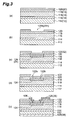
- Fig. 3 is a sectional view showing manufacturing steps of the photodetector.
- a deposited structure of semiconductor layers is formed on an n-type InAs substrate 112(12).
- n-type InAs substrate 112 As shown in Fig. 3(a) , formed on the n-type InAs substrate 112 is an n-type InAs buffer layer 114(14), an n-type InAs light absorbing layer 116(16), and an n-type InAs X P Y Sb 1-X-Y cap layer 118(18), in sequence.
- These semiconductor layers are grown by, for example, OrganoMetallic Vapor Phase Epitaxy (OMVPE), Liquid Phase Epitaxy (LPE), or Molecular Beam Epitaxy (MBE).
- OMVPE OrganoMetallic Vapor Phase Epitaxy
- LPE Liquid Phase Epitaxy
- MBE Molecular Beam Epitaxy
- the n-type InAs buffer layer 114 and the n-type InAs light absorbing layer 116 are formed, in sequence.
- the supply of the group V material gas containing As is stopped and a supply of a group V material gas containing P and Sb is started to form an n-type InAs X P Y Sb 1-X-Y cap layer (X ⁇ 0, Y>0) 118(18).
- the supply of the V group material gas is stopped when the cap 118 is formed.
- the supply of the group V material gas containing As may be continued.
- a first inorganic insulating film 120(20) is formed as a protecting film on the cap layer 118.
- the first inorganic insulating film 120 is grown by Chemical Vapor Deposition (CVD).
- a central portion of the first inorganic insulating film 120 is removed by etching using photolithography to form an almost circular opening portion 120h (20h) in the deposition direction.
- the p-type impurity is thermally diffused from the cap layer 118 to an upper layer of the light absorbing layer 116 by use of the opening portion 120h of the first inorganic insulating film 120 to form a p-type impurity semiconductor region 124(24).
- a second inorganic insulating film 122(22) is formed on the first inorganic insulating film 120 and the p-type impurity semiconductor region 124.
- the second inorganic insulating film 122 is grown by Chemical Vapor Deposition.
- a central portion of the second inorganic insulating film 122 is removed in a ring shape by etching using photolithography to form a ring-shaped opening portion 122h in the deposition direction.
- a ring-shaped contact layer and a ring-shaped wiring electrode 126(26) are formed in this opening portion 122h, in order.
- a wiring electrode 128(28) is formed.
- the p-n junction portion formed by the p-type impurity semiconductor region 24 and the n-type light absorbing layer 16 is coated with the inorganic insulating film excellent in moisture resistance. Accordingly, not only can reliability be improved, but dark current can also be reduced. Furthermore, since the layers other than the p-type impurity semiconductor region 24 including the light receiving region 24m are coated double with the first inorganic insulating film 20 and the second inorganic insulating film 22, dark current can further be reduced.
- the thickness of the cap layer 18 is 0.8 ⁇ m or more and 1.4 ⁇ m or less, dark current can be reduced without greatly increasing light absorption in the p-type impurity semiconductor region 24 that is formed by diffusing the p-type impurity into the cap layer 18, or without greatly increasing the diffusion time of the p-type impurity semiconductor region 24, more specifically, the manufacturing time of the photodetector 1.
- the light absorbing layer 16 and the cap layer 18 are formed of InAs and InAs X P Y Sb 1-X-Y , respectively, having a high degree of lattice matching, the degree of lattice matching between the light absorbing layer 16 and the cap layer 18 can be improved, and crystal distortion can be reduced.
- the photodetector 1 of the first embodiment since the p-type impurity semiconductor region 24 reaches from the cap layer 18 to the upper layer of the n-type light absorbing layer 16, a sufficient absorption length can be secured to the wavelength of a to-be-detected light (for example, light in the infrared region). As a result, the light receiving sensitivity to the wavelength of a to-be-detected light can be improved.
- a to-be-detected light for example, light in the infrared region
- Fig. 4 is a sectional view showing a photodetector according to a second embodiment of the present invention.
- the photodetector 1A shown in Fig. 4 differs from the first embodiment 1 in configuration including a first inorganic insulating film 20A, a second inorganic insulating film 22A, a p-type impurity semiconductor region 24A, and a wiring electrode 26A, respectively, in place of the first inorganic insulating film 20, the second inorganic insulating film 22, the p-type impurity semiconductor region 24, and the wiring electrode 26 in the photodetector 1.
- Other aspects of the configuration of the photodetector 1A are the same as those of the first embodiment.
- the first inorganic insulating film 20A is formed on the cap layer 18.
- identical material to that of the first inorganic insulating film 20 mentioned above is used.
- the p-type impurity semiconductor region 24A is formed in a central portion of the cap layer 18 and a central portion of an upper layer of the light absorbing layer 16 viewed from the light receiving surface side.
- the p-type impurity semiconductor region 24A is formed by ion-implanting the p-type impurity via the first inorganic insulating film 20A.
- the depth of the p-type impurity semiconductor region 24A reaches from the cap layer 18 to the upper layer of the light absorbing layer 16.
- the p-type impurity is identical to the p-type impurity in the p-type impurity semiconductor region 24 mentioned above.
- a p-n junction is formed at a boundary between the p-type impurity semiconductor region 24A and the n-type light absorbing layer 16.
- the second inorganic insulating film 22A is formed on the first inorganic insulating film 20A.
- the second inorganic insulating film 22A identical material to that of the second inorganic insulating film 22 mentioned above is used.
- the first inorganic insulating film 20A and the second inorganic insulating film 22A function as protecting layers of the semiconductor layer and reflection preventing films of incident light.
- a ring-shaped opening portion is provided, and formed in this opening portion is a contact layer (not shown) and a wiring electrode 26A, in order. Since the diameter of the ring-shaped opening portion is smaller than that of the p-type introity semiconductor region 24A, the wiring electrode 26A is electrically connected to the p-type impurity semiconductor region 24A via the contact layer.
- the contact layer and the wiring electrode 26A identical materials to those of the contact layer and the wiring electrode 26 described above are used, respectively.
- Fig. 5 is a sectional view showing manufacturing steps of the photodetector.
- n-type InAs substrate 112(12) formed on the n-type InAs substrate 112(12) is an n-type InAs buffer layer 114(14), an n-type InAs light absorbing layer 116(16), an n-type InAs X P Y Sb 1-X-Y cap layer 118(18) (X ⁇ 0, Y>0), and a first inorganic insulating film 120A (20A), in sequence.
- the p-type impurity is ion-implanted via the first inorganic insulating film 120A from the cap layer 118 to an upper layer of the light absorbing layer 116 to form a p-type impurity semiconductor region 124A(24A).
- the resist used for the mask is removed, and then an annealing treatment by heating is performed. This activates the implanted p-type impurity and reduces implantation damage.
- a second inorganic insulating film 122A(22A) is formed on the first inorganic insulating film 120A.
- a central portion of the first inorganic insulating film 120A and the second inorganic insulating film 122A is removed by etching using photolithography to form a ring-shaped opening portion 122h in the deposition direction.
- a ring-shaped contact layer and a ring-shaped wiring electrode 126A(26A) are formed in this opening portion 122h, in order.
- a wiring electrode 128(28) is formed.
- the p-n junction portion formed by the p-type impurity semiconductor region 24A and the n-type light absorbing layer 16 is coated double with the inorganic insulating films excellent in moisture resistance. Accordingly, not only can reliability be improved, but dark current can also be reduced.
- the thickness of the cap layer 18 is 0.8 ⁇ m or more and 1.4 ⁇ m or less, dark current can be reduced without greatly increasing light absorption in the p-type impurity semiconductor region 24 that is formed by ion-implanting the p-type impurity into the cap layer 18, or without greatly increasing the ion implantation time of the p-type impurity semiconductor region 24, more specifically, the manufacturing time of the photodetector 1.
- the degree of lattice matching between the light absorbing layer 16 and the cap layer 18 can be improved, and crystal distortion can be reduced.
- the photodetector 1A of the second embodiment since the p-type impurity semiconductor region 24A reaches from the cap layer 18 to the upper layer of the n-type light absorbing layer 16, a sufficient absorption length can be secured to the wavelength of a to-be-detected light (for example, light in the infrared region). As a result, the light receiving sensitivity to the wavelength of a to-be-detected light can be improved.
- a to-be-detected light for example, light in the infrared region
- Fig. 6 is a sectional view showing a photodetector according to a third embodiment of the present invention.
- the photodetector 1B shown in Fig. 6 differs from the first embodiment 1 in configuration including a p-type impurity semiconductor region 24B in place of the p-type impurity semiconductor region 24 in the photodetector 1.
- Other aspects of the configuration of the photodetector 1B are the same as those of the first embodiment.
- the upper layer of a region including the light receiving region 24m is scraped in the p-type impurity semiconductor region 24.
- the thickness of the light receiving region 24m in the p-type impurity semiconductor region 24B is made thinner than the thickness of a non-light receiving region 24n and the thickness of the cap layer 18.
- the same advantages as those of the photodetector 1 of the first embodiment can be obtained. Furthermore, according to the photodetector 1B of the third embodiment, the thickness of the light receiving region 24m in the p-type impurity semiconductor region 24B can be reduced without reducing the thickness of the cap layer 18, and thus light absorption in the p-type impurity semiconductor region 24B can be reduced without increasing dark current.
- Fig. 7 is a sectional view showing a photodetector according to a fourth embodiment of the present invention.
- the photodetector 1C shown in Fig. 7 differs from the first embodiment 1 in configuration including a cap layer 18A in place of the cap layer 18 in the photodetector 1.
- Other aspects of the configuration of the photodetector 1C are the same as those of the first embodiment.
- the cap layer 18A is made from InAs X P Y Sb 1-X-Y (X ⁇ 0, Y>0) as with the cap layer 18, and the composition ratio of As, P, and Sb is adjusted so that the degree of lattice matching between the cap layer 18A and the light absorbing layer 16 becomes within ⁇ 0.1%.
- the cap layer 18A is composed of an upper layer 18b and a lower layer 18c.
- the n-type impurity concentration of the upper layer 18b is the same as that of the cap layer 18.
- the lower layer 18c is a graded layer, therein the concentration distribution of an n-type impurity slopes so that the concentration increases from the light absorbing layer 16 toward the upper layer 18b of the cap layer.
- the concentration of an n-type impurity in at least a part of the lower layer 18c of the cap layer 18A increases continuously or in a graded manner, and thus the energy band gap increases from the light absorbing layer 16 toward the upper layer 18b of the cap layer continuously or in a graded manner. Accordingly, carriers migrate smoothly, which allows operating at a high speed.
- the present invention is not limited to the present embodiments mentioned above, and various modifications can be made.
- the first conductivity type was provided as the n-type, and the second conductivity type, as the p-type, however, it may also be possible to provide the first conductivity type as the p-type, and the second conductivity type, as the n-type, conversely.
- diffusion was performed by supplying the material gas containing Zn or Cd as a p-type impurity into the crystal growth furnace, however, it is possible to perform diffusion by filling a Zn compound and the substrate of Fig. 3(b) in a quartz tube and heating the same.
- the light receiving region of the p-type impurity semiconductor layer in the photodetector of the first embodiment has been thinned, however, it is possible to likewise thin the light receiving region of the p-type impurity semiconductor region in the photodetector of the second embodiment as well.
- the lower layer of the cap layer in the photodetector of the first embodiment has been provided as a graded layer, however, it is possible to provide likewise the lower layer of the cap layer as a graded layer in the photodetector of the second embodiment as well.
Landscapes
- Light Receiving Elements (AREA)
Abstract
A photodetector 1 according to an embodiment of the present invention includes: an n-type InAs substrate 12; an n-type InAs buffer layer 14 formed on the n-type InAs substrate 12; an n-type InAs light absorbing layer 16 formed on the n-type InAs buffer layer 14; an InAsxPYSb1-X-Y cap layer 18 (X≥0, Y>0) formed on the n-type InAs light absorbing layer 16; a first inorganic insulating film 20 formed on the cap layer 18, and having an opening portion 20h in a deposition direction; a p-type impurity semiconductor region 24 formed by diffusing a p-type impurity from the opening portion 20h of the first inorganic insulating film 20, and reaching from the cap layer 18 to an upper layer of the n-type InAs light absorbing layer 16; and a second inorganic insulating film 22 formed on the first inorganic insulating film 20 and on the p-type impurity semiconductor region 24.
Description
- The present invention relates to a photodetector and a manufacturing method of the photodetector.
- As photodetectors, photodiodes have been known. In
Patent Document 1, there has been described a mesa photodiode in which a p-n junction is formed by a p-type InAsPSb semiconductor layer and an n-type InAs semiconductor layer.
Patent Document 1: Japanese Published Unexamined Patent Application No.H10-233523 - However, in the mesa photodiode, since the p-n junction portion is exposed, there is a large temporal change in characteristics due to moisture absorption, and thus reliability is low. Moreover, the exposure of the p-n junction portion also causes an increase in dark current.
- Therefore, the present invention aims to provide a photodetector that allows improving reliability and reducing dark current.
- A photodetector according to the present invention includes: (a) a first conductivity-type InAs substrate; (b) a first conductivity-type InAs buffer layer formed on the first conductivity-type InAs substrate; (c) a first conductivity-type InAs light absorbing layer formed on the first conductivity-type InAs buffer layer; (d) a cap layer formed on the first conductivity-type InAs light absorbing layer, and made from InAsXPYSb1-X-Y (X≥0, Y>0) containing In and at least two of As, P, and Sb; (e) a first inorganic insulating film formed on the cap layer, and having an opening portion in a deposition direction; (f) a second conductivity-type impurity semiconductor region formed by diffusing a second conductivity-type impurity from the opening portion of the first inorganic insulating film, and reaching from the cap layer to an upper layer of the first conductivity-type InAs light absorbing layer; and (g) a second inorganic insulating film formed on the first inorganic insulating film and on the second conductivity-type impurity semiconductor layer.
- A manufacturing method of a photodetector according to the present invention includes: (1) a first deposition step of depositing, on a first conductivity-type InAs substrate, a first conductivity-type InAs buffer layer, a first conductivity-type InAs light absorbing layer, a cap layer made from InAsXPYSb1-X-Y (X≥0, Y>0) containing In and at least two of As, P, and Sb, and a first inorganic insulating film, in sequence; (2) an opening portion forming step of forming, in the first inorganic insulating film, an opening portion in a deposition direction; (3) a diffusion step of forming a second conductivity-type impurity semiconductor region by diffusing a second conductivity-type impurity from the cap layer to an upper layer of the first conductivity-type InAs light absorbing layer by use of the opening portion of the first inorganic insulating film; and (4) a second deposition step of depositing a second inorganic insulating film on the first inorganic insulating film and on the second conductivity-type impurity semiconductor layer.
- According to this photodetector, a second conductivity-type impurity semiconductor layer is formed by diffusing a second conductivity-type impurity by use of the opening portion of the first inorganic insulating film, and a second inorganic insulating film is formed on the first inorganic insulating film and on the second conductivity-type impurity semiconductor region, and thus a p-n junction formed by the second conductivity-type impurity semiconductor region and the first conductivity-type InAs light absorbing layer is coated with the inorganic insulating film excellent in moisture resistance. Accordingly, not only can reliability be improved, but dark current can also be reduced. Moreover, since the layers other than the second conductivity-type impurity semiconductor region including a light receiving region are coated double with the first inorganic insulating film and the second inorganic insulating film, dark current can further be reduced.
- Here, the degree of lattice matching between InAs and InAsxPYSb1-X-Y is high. Therefore, according to this photodetector, the degree of lattice matching between the light absorbing layer and the cap layer can be improved, and crystal distortion can be reduced. Furthermore, according to this photodetector, since the second conductivity-type impurity semiconductor region reaches from the cap layer to the upper layer of the first conductivity-type InAs light absorbing layer, a sufficient absorption length can be secured to the wavelength of a to-be-detected light. As a result, the light receiving sensitivity to the wavelength of a to-be-detected light can be improved.
- A photodetector according to the present invention includes: (a) a first conductivity-type InAs substrate; (b) a first conductivity-type InAs buffer layer formed on the first conductivity-type InAs substrate; (c) a first conductivity-type InAs light absorbing layer formed on the first conductivity-type InAs buffer layer; (d) a cap layer formed on the first conductivity-type InAs light absorbing layer, and made from InAsXPySb1-X-Y (X≥0, Y>0) containing In and at least two of As, P, and Sb; (e) a first inorganic insulating film formed on the cap layer; (f) a second conductivity-type impurity semiconductor region formed by ion-implanting a second conductivity-type impurity via the first inorganic insulating film, and reaching from the cap layer to an upper layer of the first conductivity-type InAs light absorbing layer; and (g) a second inorganic insulating film formed on the first inorganic insulating film.
- A manufacturing method of a photodetector according to the present invention includes: (1) a first deposition step of depositing, on a first conductivity-type InAs substrate, a first conductivity-type InAs buffer layer, a first conductivity-type InAs light absorbing layer, a cap layer made from InAsXPYSb1-X-Y (X≥0, Y>0) containing In and at least two of As, P, and Sb, and a first inorganic insulating film, in sequence; (2) an ion implantation step of forming a second conductivity-type impurity semiconductor region by ion-implanting a second conductivity-type impurity from the cap layer to an upper layer of the first conductivity-type InAs light absorbing layer via the first inorganic insulating film; and (3) a second deposition step of depositing a second inorganic insulating film on the first inorganic insulating film.
- According to this photodetector, a second conductivity-type impurity semiconductor region is formed by ion-implanting a second conductivity-type impurity via the first inorganic insulating film, and a second inorganic insulating film is formed on the first inorganic insulating film, and thus a p-n junction portion formed by the second conductivity-type impurity semiconductor region and the first conductivity-type InAs light absorbing layer is coated double with the inorganic insulating films excellent in moisture resistance. Accordingly, not only can reliability be improved, but dark current can also be reduced.
- As described above, since the degree of lattice matching between InAs and InAsXPYSb1-X-Y is high, in this photodetector as well, the degree of lattice matching between the light absorbing layer and the cap layer can be improved, and crystal distortion can be reduced. Furthermore, in this photodetector as well, since the second conductivity-type impurity semiconductor region reaches from the cap layer to the upper layer of the first conductivity-type InAs light absorbing layer, a sufficient absorption length can be secured to the wavelength of a to-be-detected light, so that the light receiving sensitivity to the wavelength of a to-be-detected light can be improved.
- It is preferable that the thickness of the cap layer mentioned above is 0.8µm or more and 1.4µm or less. The inventor of the present application has discovered from the analysis results of experimentation that the thicker the cap layer, the more the dark current is reduced in magnitude. In this photodetector, since the thickness of the cap layer is 0.8µm or more, dark current can further be reduced. Moreover, since the thickness of the cap layer is 1.4µm or less, an increase in light absorption in the second conductivity-type impurity semiconductor region that is formed by doping a second conductivity-type impurity into the cap layer can be suppressed, and an increase in diffusion time or ion implantation time of the second conductivity-type impurity semiconductor region, more specifically, an increase in manufacturing time of the photodetector can be suppressed.
- Moreover, it is preferable that the thickness of a light receiving region in the second conductivity-type impurity semiconductor region mentioned above is thinner than the thickness of the cap layer. According to this, the thickness of the light receiving region in the second conductivity-type impurity semiconductor region can be reduced without reducing the thickness of the cap layer, and thus light absorption in the second conductivity-type impurity semiconductor region can be reduced without increasing dark current.
- Moreover, it is preferable that the cap layer mentioned above contains a first conductivity-type impurity, and a concentration distribution of the first conductivity-type impurity in at least a part of a lower layer of the cap layer slopes so that the concentration increases from the first conductivity-type InAs light absorbing layer toward the cap layer. According to this configuration, the concentration of a first conductivity-type impurity in at least a part of the lower layer of the cap layer increases continuously or in a graded manner, and thus the energy band gap increases from the light absorbing layer toward the cap layer continuously or in a graded manner. Accordingly, carriers migrate smoothly, which allows operating at a high speed.
- The present invention allows improving reliability of a photodetector and reducing dark current.
-
- [
Fig. 1 ] A view showing a photodetector according to a first embodiment of the present invention. - [
Fig. 2 ] Measurement results of dark current to the thickness of a cap layer. - [
Fig. 3 ] A sectional view showing manufacturing steps of the photodetector shown inFig. 1 . - [
Fig. 4 ] A sectional view showing a photodetector according to a second embodiment of the present invention. - [
Fig. 5 ] A sectional view showing manufacturing steps of the photodetector shown inFig. 4 . - [
Fig. 6 ] A sectional view showing a photodetector according to a third embodiment of the present invention. - [
Fig. 7 ] A sectional view showing a photodetector according to a fourth embodiment of the present invention. - 1, 1A, 1B, 1C ... photodetector, 12 ... n-type InAs substrate, 14 ... n-type InAs buffer layer, 16 ... n-type InAs light absorbing layer, 18, 18A ... n-type InAsXPYSb1-X-Y cap layer, 20, 20A ... first inorganic insulating film, 20h ... opening portion, 22, 22A ... second inorganic insulating film, 24, 24A, 24B ... p-type impurity semiconductor layer, 24m... light receiving region, 26, 26A, 28 ... wiring electrode.
- Hereinafter, preferred embodiments of the present invention will be described in detail with reference to the drawings. Also, the same or corresponding parts are denoted with the same reference numerals and characters in each drawing.
-
Fig. 1 is a view showing a photodetector according to a first embodiment of the present invention. InFig. 1(a) , shown is a photodetector viewed from a light receiving surface side, and inFig. 1(b) , shown is a sectional view along a line I-I inFig. 1(a) . - The
photodetector 1 shown inFig. 1 is a planar photodiode. In thephotodetector 1, deposited on an n-type (first conductivity-type)InAs substrate 12 is an n-typeInAs buffer layer 14, an n-type InAslight absorbing layer 16, an n-type InAsXPYSb1-X-Y cap layer 18 (X≥0, Y>0), a first inorganicinsulating film 20, and a secondinorganic insulating film 22, in sequence. - In a central portion of the first inorganic
insulating film 20 viewed from the light receiving surface side, an almostcircular opening portion 20h opened in the deposition direction is formed, and by diffusing a p-type (second conductivity-type) impurity from thisopening portion 20h, a p-typeimpurity semiconductor region 24 is formed. The depth of the p-typeimpurity semiconductor region 24 reaches from thecap layer 18 to an upper layer of thelight absorbing layer 16. As the p-type impurity, for example, Zn or Cd is used. Thus, a p-n junction is formed at a boundary between the p-typeimpurity semiconductor region 24 and the n-typelight absorbing layer 16. - The impurity concentration of the
light absorbing layer 16 is lower than that of the p-typeimpurity semiconductor region 24. This makes it likely that a depletion layer to be generated in the vicinity of the p-n junction portion spreads to thelight absorbing layer 16 side, and the thickness of the depletion layer results in a large thickness. As a result, the light receiving sensitivity is improved. In order to improve crystallinity of thelight absorbing layer 16, thebuffer layer 14 and thecap layer 18 are provided so as to sandwich thelight absorbing layer 16 therebetween. - The
cap layer 18 is made from InAsXPYSb1-X-Y including at least P and Sb out of As, P, and Sb, besides In. Here, X denotes a composition ratio of As. As will be described later, X results in zero or more due to the manufacturing method. The InAsXPYSb1-X-Y can have lattice matching with InAs at a high degree of lattice matching. In the present embodiment, the composition ratio of As, P, and Sb is adjusted so that the degree of lattice matching between thecap layer 18 and thelight absorbing layer 16 becomes within ±0.1%. Moreover, the thickness of thecap layer 18 is preferably 0.8µm or more and 1.4µm or less, and more preferably, 1.0µm or more and 1.4µm or less. -
Fig. 2 shows measurement results of dark current to the thickness of a cap layer. According toFig. 2 , it can be understood that, as thecap layer 18 is made thicker, the dark current begins to decrease from 0.7µm, and at 1.0µm, the dark current has decreased to the order of nano amperes. Thus, if the thickness of thecap layer 18 is 0.8µm or more, the dark current can be reduced. If the thickness of thecap layer 18 is 1.0µm or more, the dark current can further be reduced. - Moreover, if the thickness of the
cap layer 18 is 1.4µm or less, an increase in light absorption in the p-typeimpurity semiconductor region 24 formed by dispersing a p-type impurity into thecap layer 18 can be suppressed, and an increase in diffusion time of the p-typeimpurity semiconductor layer 24, more specifically, an increase in manufacturing time of thephotodetector 1 can be suppressed. - Returning to
Fig. 1 , as the material of the first inorganic insulatingfilm 20 and the second inorganic insulatingfilm 22, for example, Si3N4 or SiO2 is used. These inorganic insulating films are excellent in moisture resistance. - The second inorganic insulating
film 22 is formed on the p-typeimpurity semiconductor region 24 and the first inorganic insulatingfilm 20. The second inorganic insulatingfilm 22 functions as a protecting layer of theopening portion 20h used for a formation of the p-n junction portion and a reflection preventing film of a to-be-detected light that is made incident into alight receiving region 24m. - In this second inorganic insulating
film 22, a ring-shaped opening portion is provided in the deposition direction, and a ring-shaped contact layer (not shown) and a ring-shapedwiring electrode 26 are provided in this opening portion, in order. Since the diameter of the opening portion is smaller than that of theopening portion 20h of the first inorganic insulatingfilm 20, thewiring electrode 26 is electrically connected to the p-typeimpurity semiconductor layer 24 via the contact layer. As the material of the contact layer, for example, a material having high ohmic properties such as AuZn or Ti/Pt/Au is used, and as the material of thewiring electrode 26, for example, Ti/Pt/Au, Ti/Pt/AuZn, Ti/Au, or Cr/Au is used. - Moreover, a
wiring electrode 28 is provided on the lower side of thesubstrate 12. As the material of thewiring electrode 28, for example, AuGe/Ni/Au is used. - Next, description will be given of a manufacturing method of the
photodetector 1.Fig. 3 is a sectional view showing manufacturing steps of the photodetector. - First, a deposited structure of semiconductor layers is formed on an n-type InAs substrate 112(12). As shown in
Fig. 3(a) , formed on the n-type InAs substrate 112 is an n-type InAs buffer layer 114(14), an n-type InAs light absorbing layer 116(16), and an n-type InAsXPYSb1-X-Y cap layer 118(18), in sequence. These semiconductor layers are grown by, for example, OrganoMetallic Vapor Phase Epitaxy (OMVPE), Liquid Phase Epitaxy (LPE), or Molecular Beam Epitaxy (MBE). In the following, OrganoMetallic Vapor Phase Epitaxy will be exemplified. - First, by supplying a group III material gas containing In and a group V material gas containing As into a crystal growth furnace, the n-type
InAs buffer layer 114 and the n-type InAs light absorbinglayer 116 are formed, in sequence. Next, the supply of the group V material gas containing As is stopped and a supply of a group V material gas containing P and Sb is started to form an n-type InAsXPYSb1-X-Y cap layer (X≥0, Y>0) 118(18). Thus, the supply of the V group material gas is stopped when thecap 118 is formed. However, there may be a case where As remains in the crystal growth furnace, so that the composition ratio X of As in the formedcap layer 118 results in zero or more. Also, the supply of the group V material gas containing As may be continued. - Subsequently, a first inorganic insulating film 120(20) is formed as a protecting film on the
cap layer 118. The first inorganic insulatingfilm 120 is grown by Chemical Vapor Deposition (CVD). - Then, as shown in
Fig. 3(b) , a central portion of the first inorganic insulatingfilm 120 is removed by etching using photolithography to form an almostcircular opening portion 120h (20h) in the deposition direction. - Then, as shown in
Fig. 3(c) , by supplying a material gas containing Zn or Cd as a p-type impurity into the crystal growth furnace, the p-type impurity is thermally diffused from thecap layer 118 to an upper layer of thelight absorbing layer 116 by use of theopening portion 120h of the first inorganic insulatingfilm 120 to form a p-type impurity semiconductor region 124(24). - Then, a second inorganic insulating film 122(22) is formed on the first inorganic insulating
film 120 and the p-typeimpurity semiconductor region 124. The second inorganic insulatingfilm 122 is grown by Chemical Vapor Deposition. - Then, as shown in
Fig. 3(d) , a central portion of the second inorganic insulatingfilm 122 is removed in a ring shape by etching using photolithography to form a ring-shapedopening portion 122h in the deposition direction. Thereafter, as shown inFig. 3(e) , a ring-shaped contact layer and a ring-shaped wiring electrode 126(26) are formed in thisopening portion 122h, in order. Next, after the bottom surface of thesubstrate 112 is scraped to a predetermined thickness, a wiring electrode 128(28) is formed. - Thus, according to the
photodetector 1 of the first embodiment, the p-n junction portion formed by the p-typeimpurity semiconductor region 24 and the n-typelight absorbing layer 16 is coated with the inorganic insulating film excellent in moisture resistance. Accordingly, not only can reliability be improved, but dark current can also be reduced. Furthermore, since the layers other than the p-typeimpurity semiconductor region 24 including thelight receiving region 24m are coated double with the first inorganic insulatingfilm 20 and the second inorganic insulatingfilm 22, dark current can further be reduced. - Moreover, according to the
photodetector 1 of the first embodiment, since the thickness of thecap layer 18 is 0.8µm or more and 1.4µm or less, dark current can be reduced without greatly increasing light absorption in the p-typeimpurity semiconductor region 24 that is formed by diffusing the p-type impurity into thecap layer 18, or without greatly increasing the diffusion time of the p-typeimpurity semiconductor region 24, more specifically, the manufacturing time of thephotodetector 1. - Moreover, according to the
photodetector 1 of the first embodiment, since thelight absorbing layer 16 and thecap layer 18 are formed of InAs and InAsXPYSb1-X-Y, respectively, having a high degree of lattice matching, the degree of lattice matching between the light absorbinglayer 16 and thecap layer 18 can be improved, and crystal distortion can be reduced. - Moreover, according to the
photodetector 1 of the first embodiment, since the p-typeimpurity semiconductor region 24 reaches from thecap layer 18 to the upper layer of the n-typelight absorbing layer 16, a sufficient absorption length can be secured to the wavelength of a to-be-detected light (for example, light in the infrared region). As a result, the light receiving sensitivity to the wavelength of a to-be-detected light can be improved. -
Fig. 4 is a sectional view showing a photodetector according to a second embodiment of the present invention. Thephotodetector 1A shown inFig. 4 differs from thefirst embodiment 1 in configuration including a first inorganic insulatingfilm 20A, a second inorganic insulatingfilm 22A, a p-typeimpurity semiconductor region 24A, and awiring electrode 26A, respectively, in place of the first inorganic insulatingfilm 20, the second inorganic insulatingfilm 22, the p-typeimpurity semiconductor region 24, and thewiring electrode 26 in thephotodetector 1. Other aspects of the configuration of thephotodetector 1A are the same as those of the first embodiment. - The first inorganic insulating
film 20A is formed on thecap layer 18. For the first inorganic insulatingfilm 20A, identical material to that of the first inorganic insulatingfilm 20 mentioned above is used. - In a central portion of the
cap layer 18 and a central portion of an upper layer of thelight absorbing layer 16 viewed from the light receiving surface side, the p-typeimpurity semiconductor region 24A is formed. The p-typeimpurity semiconductor region 24A is formed by ion-implanting the p-type impurity via the first inorganic insulatingfilm 20A. The depth of the p-typeimpurity semiconductor region 24A reaches from thecap layer 18 to the upper layer of thelight absorbing layer 16. The p-type impurity is identical to the p-type impurity in the p-typeimpurity semiconductor region 24 mentioned above. Thus, a p-n junction is formed at a boundary between the p-typeimpurity semiconductor region 24A and the n-typelight absorbing layer 16. - The second inorganic insulating
film 22A is formed on the first inorganic insulatingfilm 20A. For the second inorganic insulatingfilm 22A, identical material to that of the second inorganic insulatingfilm 22 mentioned above is used. The first inorganic insulatingfilm 20A and the second inorganic insulatingfilm 22A function as protecting layers of the semiconductor layer and reflection preventing films of incident light. - In a central portion of these first and second inorganic insulating
films wiring electrode 26A, in order. Since the diameter of the ring-shaped opening portion is smaller than that of the p-typeimpunity semiconductor region 24A, thewiring electrode 26A is electrically connected to the p-typeimpurity semiconductor region 24A via the contact layer. For the contact layer and thewiring electrode 26A, identical materials to those of the contact layer and thewiring electrode 26 described above are used, respectively. - Next, description will be given of a manufacturing method of the
photodetector 1A.Fig. 5 is a sectional view showing manufacturing steps of the photodetector. - First, as shown in
Fig. 5(a) , in the same manner as in the first embodiment, formed on the n-type InAs substrate 112(12) is an n-type InAs buffer layer 114(14), an n-type InAs light absorbing layer 116(16), an n-type InAsXPYSb1-X-Y cap layer 118(18) (X≥0, Y>0), and a first inorganic insulatingfilm 120A (20A), in sequence. - Then, as shown in
Fig. 5(b) , by implanting ions of Zn or Cd as a p-type impurity into a central portion of the first inorganic insulatingfilm 120A from the light receiving surface side using a resist prepared by photolithography (not shown) as a mask, the p-type impurity is ion-implanted via the first inorganic insulatingfilm 120A from thecap layer 118 to an upper layer of thelight absorbing layer 116 to form a p-typeimpurity semiconductor region 124A(24A). Subsequently, the resist used for the mask is removed, and then an annealing treatment by heating is performed. This activates the implanted p-type impurity and reduces implantation damage. - Next, as shown in
Fig. 5(c) , in the same manner as in the first embodiment, a second inorganic insulatingfilm 122A(22A) is formed on the first inorganic insulatingfilm 120A. - Then, as shown in
Fig. 5(d) , a central portion of the first inorganic insulatingfilm 120A and the second inorganic insulatingfilm 122A is removed by etching using photolithography to form a ring-shapedopening portion 122h in the deposition direction. Thereafter, as shown inFig. 5(e) , a ring-shaped contact layer and a ring-shapedwiring electrode 126A(26A) are formed in thisopening portion 122h, in order. Next, after the bottom surface of thesubstrate 112 is scraped to a predetermined thickness, a wiring electrode 128(28) is formed. - Thus, according to the
photodetector 1A of the second embodiment, the p-n junction portion formed by the p-typeimpurity semiconductor region 24A and the n-typelight absorbing layer 16 is coated double with the inorganic insulating films excellent in moisture resistance. Accordingly, not only can reliability be improved, but dark current can also be reduced. - Moreover, in the
photodetector 1A of the second embodiment as well, since the thickness of thecap layer 18 is 0.8µm or more and 1.4µm or less, dark current can be reduced without greatly increasing light absorption in the p-typeimpurity semiconductor region 24 that is formed by ion-implanting the p-type impurity into thecap layer 18, or without greatly increasing the ion implantation time of the p-typeimpurity semiconductor region 24, more specifically, the manufacturing time of thephotodetector 1. - Moreover, in the
photodetector 1 A of the second embodiment as well, since thelight absorbing layer 16 and thecap layer 18 are formed of InAs and InAsXPYSb1-X-Y, respectively, having a high degree of lattice matching, the degree of lattice matching between the light absorbinglayer 16 and thecap layer 18 can be improved, and crystal distortion can be reduced. - Moreover, in the
photodetector 1A of the second embodiment as well, since the p-typeimpurity semiconductor region 24A reaches from thecap layer 18 to the upper layer of the n-typelight absorbing layer 16, a sufficient absorption length can be secured to the wavelength of a to-be-detected light (for example, light in the infrared region). As a result, the light receiving sensitivity to the wavelength of a to-be-detected light can be improved. -
Fig. 6 is a sectional view showing a photodetector according to a third embodiment of the present invention. Thephotodetector 1B shown inFig. 6 differs from thefirst embodiment 1 in configuration including a p-typeimpurity semiconductor region 24B in place of the p-typeimpurity semiconductor region 24 in thephotodetector 1. Other aspects of the configuration of thephotodetector 1B are the same as those of the first embodiment. - In the p-type
impurity semiconductor region 24B, the upper layer of a region including thelight receiving region 24m is scraped in the p-typeimpurity semiconductor region 24. In this manner, the thickness of thelight receiving region 24m in the p-typeimpurity semiconductor region 24B is made thinner than the thickness of anon-light receiving region 24n and the thickness of thecap layer 18. - In the
photodetector 1B of the third embodiment as well, the same advantages as those of thephotodetector 1 of the first embodiment can be obtained. Furthermore, according to thephotodetector 1B of the third embodiment, the thickness of thelight receiving region 24m in the p-typeimpurity semiconductor region 24B can be reduced without reducing the thickness of thecap layer 18, and thus light absorption in the p-typeimpurity semiconductor region 24B can be reduced without increasing dark current. -
Fig. 7 is a sectional view showing a photodetector according to a fourth embodiment of the present invention. Thephotodetector 1C shown inFig. 7 differs from thefirst embodiment 1 in configuration including acap layer 18A in place of thecap layer 18 in thephotodetector 1. Other aspects of the configuration of thephotodetector 1C are the same as those of the first embodiment. - The
cap layer 18A is made from InAsXPYSb1-X-Y (X≥0, Y>0) as with thecap layer 18, and the composition ratio of As, P, and Sb is adjusted so that the degree of lattice matching between thecap layer 18A and thelight absorbing layer 16 becomes within ±0.1%. Thecap layer 18A is composed of anupper layer 18b and alower layer 18c. The n-type impurity concentration of theupper layer 18b is the same as that of thecap layer 18. On the other hand, thelower layer 18c is a graded layer, therein the concentration distribution of an n-type impurity slopes so that the concentration increases from thelight absorbing layer 16 toward theupper layer 18b of the cap layer. - In the
photodetector 1C of the fourth embodiment as well, the same advantages as those of thephotodetector 1 of the first embodiment can be obtained. Furthermore, according to thephotodetector 1C of the fourth embodiment, the concentration of an n-type impurity in at least a part of thelower layer 18c of thecap layer 18A increases continuously or in a graded manner, and thus the energy band gap increases from thelight absorbing layer 16 toward theupper layer 18b of the cap layer continuously or in a graded manner. Accordingly, carriers migrate smoothly, which allows operating at a high speed. - Also, the present invention is not limited to the present embodiments mentioned above, and various modifications can be made. For example, in the above-mentioned embodiments, the first conductivity type was provided as the n-type, and the second conductivity type, as the p-type, however, it may also be possible to provide the first conductivity type as the p-type, and the second conductivity type, as the n-type, conversely.
- Moreover, in the first embodiment, when the p-type impurity semiconductor region is prepared, diffusion was performed by supplying the material gas containing Zn or Cd as a p-type impurity into the crystal growth furnace, however, it is possible to perform diffusion by filling a Zn compound and the substrate of
Fig. 3(b) in a quartz tube and heating the same. - Moreover, in the fourth embodiment, the light receiving region of the p-type impurity semiconductor layer in the photodetector of the first embodiment has been thinned, however, it is possible to likewise thin the light receiving region of the p-type impurity semiconductor region in the photodetector of the second embodiment as well.
- Moreover, in the fourth embodiment, the lower layer of the cap layer in the photodetector of the first embodiment has been provided as a graded layer, however, it is possible to provide likewise the lower layer of the cap layer as a graded layer in the photodetector of the second embodiment as well.
Claims (7)
- A photodetector comprising:a first conductivity-type InAs substrate;a first conductivity-type InAs buffer layer formed on the first conductivity-type InAs substrate;a first conductivity-type InAs light absorbing layer formed on the first conductivity-type InAs buffer layer;a cap layer formed on the first conductivity-type InAs light absorbing layer, and made from InAsXPYSb1-X-Y (X≥0, Y>0) containing In and at least two of As, P, and Sb;a first inorganic insulating film formed on the cap layer, and having an opening portion in a deposition direction;a second conductivity-type impurity semiconductor region formed by diffusing a second conductivity-type impurity from the opening portion of the first inorganic insulating film, and reaching from the cap layer to an upper layer of the first conductivity-type InAs light absorbing layer; anda second inorganic insulating film formed on the first inorganic insulating film and on the second conductivity-type impurity semiconductor region.
- A photodetector comprising:a first conductivity-type InAs substrate;a first conductivity-type InAs buffer layer formed on the first conductivity-type InAs substrate;a first conductivity-type InAs light absorbing layer formed on the first conductivity-type InAs buffer layer;a cap layer formed on the first conductivity-type InAs light absorbing layer, and made from InAsXPYSb1-X-Y (X≥0, Y>0) containing In and at least two of As, P, and Sb;a first inorganic insulating film formed on the cap layer;a second conductivity-type impurity semiconductor region formed by ion-implanting a second conductivity-type impurity via the first inorganic insulating film, and reaching from the cap layer to an upper layer of the first conductivity-type InAs light absorbing layer; anda second inorganic insulating film formed on the first inorganic insulating film.
- The photodetector according to Claim 1 or 2, wherein
the thickness of the cap layer is 0.8µm or more and 1.4µm or less. - The photodetector according to any one of Claims 1 to 3, wherein
the thickness of a light receiving region in the second conductivity-type impurity semiconductor layer is thinner than the thickness of the cap layer. - The photodetector according to any one of Claims 1 to 4, wherein
the cap layer contains a first conductivity-type impurity, and
a concentration distribution of the first conductivity-type impurity in at least a part of a lower layer of the cap layer slopes so that the concentration increases from the first conductivity-type InAs light absorbing layer toward the cap layer. - A manufacturing method of a photodetector comprising:
a first deposition step of depositing, on a first conductivity-type InAs substrate, a first conductivity-type InAs buffer layer, a first conductivity-type InAs light absorbing layer, a cap layer made from InAsXPYSb1-X-Y (X≥0, Y>0) containing In and at least two of As, P, and Sb, and a first inorganic insulating film, in sequence;
an opening portion forming step of forming, in the first inorganic insulating film, an opening portion in a deposition direction;
a diffusion step of forming a second conductivity-type impurity semiconductor region by diffusing a second conductivity-type impurity from the cap layer to an upper layer of the first conductivity-type InAs light absorbing layer by use of the opening portion of the first inorganic insulating film; and
a second deposition step of depositing a second inorganic insulating film on the first inorganic insulating film and on the second conductivity-type impurity semiconductor region. - A manufacturing method of a photodetector comprising:
a first deposition step of depositing, on a first conductivity-type InAs substrate, a first conductivity-type InAs buffer layer, a first conductivity-type InAs light absorbing layer, a cap layer made from InAsXPYSb1-X-Y (X≥0, Y>0) containing In and at least two of As, P, and Sb, and a first inorganic insulating film, in sequence;
an ion implantation step of forming a second conductivity-type impurity semiconductor region by ion-implanting a second conductivity-type impurity from the cap layer to an upper layer of the first conductivity-type InAs light absorbing layer via the first inorganic insulating film; and
a second deposition step of depositing a second inorganic insulating film on the first inorganic insulating film.
Applications Claiming Priority (2)
| Application Number | Priority Date | Filing Date | Title |
|---|---|---|---|
| JP2006232546A JP2008060161A (en) | 2006-08-29 | 2006-08-29 | Photodetector and method for manufacturing the same |
| PCT/JP2007/066539 WO2008026536A1 (en) | 2006-08-29 | 2007-08-27 | Photodetector and method for manufacturing photodetector |
Publications (1)
| Publication Number | Publication Date |
|---|---|
| EP2058871A1 true EP2058871A1 (en) | 2009-05-13 |
Family
ID=39135819
Family Applications (1)
| Application Number | Title | Priority Date | Filing Date |
|---|---|---|---|
| EP07793014A Withdrawn EP2058871A1 (en) | 2006-08-29 | 2007-08-27 | Photodetector and method for manufacturing photodetector |
Country Status (7)
| Country | Link |
|---|---|
| US (2) | US8101940B2 (en) |
| EP (1) | EP2058871A1 (en) |
| JP (1) | JP2008060161A (en) |
| KR (1) | KR20090056934A (en) |
| CN (1) | CN101506998B (en) |
| TW (1) | TW200830570A (en) |
| WO (1) | WO2008026536A1 (en) |
Families Citing this family (5)
| Publication number | Priority date | Publication date | Assignee | Title |
|---|---|---|---|---|
| JP2010177350A (en) * | 2009-01-28 | 2010-08-12 | Hamamatsu Photonics Kk | Infrared detecting element |
| JP6518076B2 (en) * | 2015-02-16 | 2019-05-22 | エイブリック株式会社 | Photodetecting semiconductor device having light receiving element |
| RU2726903C1 (en) * | 2019-11-19 | 2020-07-16 | Общество с ограниченной ответственностью "ИоффеЛЕД" | Method for manufacturing photodiodes of the medium-wave ir spectral range |
| TWI838047B (en) * | 2022-12-27 | 2024-04-01 | 台亞半導體股份有限公司 | Photodiode structure |
| WO2026079600A1 (en) * | 2024-10-10 | 2026-04-16 | 엘지이노텍 주식회사 | Photodetector |
Family Cites Families (10)
| Publication number | Priority date | Publication date | Assignee | Title |
|---|---|---|---|---|
| JPH01194352A (en) * | 1988-01-28 | 1989-08-04 | Fujitsu Ltd | Photo detector and integrated receiver |
| JPH022691A (en) | 1988-06-17 | 1990-01-08 | Nec Corp | Semiconductor light receiving device |
| JPH07123170B2 (en) * | 1990-08-07 | 1995-12-25 | 光計測技術開発株式会社 | Light receiving element |
| JPH04152670A (en) * | 1990-10-17 | 1992-05-26 | Nec Corp | Manufacture of photodetector |
| JPH10233523A (en) * | 1997-02-18 | 1998-09-02 | Hamamatsu Photonics Kk | Photo detector |
| JPH10233532A (en) | 1997-02-21 | 1998-09-02 | Houshin Kagaku Sangiyoushiyo:Kk | Light emitting diode |
| JP3370298B2 (en) * | 1999-07-27 | 2003-01-27 | シャープ株式会社 | Photodetector with built-in circuit |
| JP2001177142A (en) * | 1999-12-16 | 2001-06-29 | Hamamatsu Photonics Kk | Light receiving element |
| JP2001194352A (en) | 2000-01-05 | 2001-07-19 | Kansai X Sen Kk | Ultrasonic inspection equipment for tubular members |
| JP2005260118A (en) * | 2004-03-15 | 2005-09-22 | Sumitomo Electric Ind Ltd | Light receiving element and manufacturing method thereof |
-
2006
- 2006-08-29 JP JP2006232546A patent/JP2008060161A/en active Pending
-
2007
- 2007-08-27 WO PCT/JP2007/066539 patent/WO2008026536A1/en not_active Ceased
- 2007-08-27 EP EP07793014A patent/EP2058871A1/en not_active Withdrawn
- 2007-08-27 KR KR1020087031857A patent/KR20090056934A/en not_active Ceased
- 2007-08-27 CN CN2007800315052A patent/CN101506998B/en not_active Expired - Fee Related
- 2007-08-27 US US12/439,234 patent/US8101940B2/en not_active Expired - Fee Related
- 2007-08-29 TW TW096132116A patent/TW200830570A/en unknown
-
2011
- 2011-11-10 US US13/293,801 patent/US8263966B2/en not_active Expired - Fee Related
Non-Patent Citations (1)
| Title |
|---|
| See references of WO2008026536A1 * |
Also Published As
| Publication number | Publication date |
|---|---|
| WO2008026536A1 (en) | 2008-03-06 |
| US20100001358A1 (en) | 2010-01-07 |
| US8101940B2 (en) | 2012-01-24 |
| US20120056243A1 (en) | 2012-03-08 |
| TW200830570A (en) | 2008-07-16 |
| JP2008060161A (en) | 2008-03-13 |
| US8263966B2 (en) | 2012-09-11 |
| CN101506998A (en) | 2009-08-12 |
| CN101506998B (en) | 2012-06-27 |
| KR20090056934A (en) | 2009-06-03 |
Similar Documents
| Publication | Publication Date | Title |
|---|---|---|
| US5144381A (en) | Semiconductor light detector utilizing an avalanche effect and having an improved guard ring structure | |
| US4904608A (en) | Pin photodiode having a low leakage current | |
| US4651187A (en) | Avalanche photodiode | |
| US5843804A (en) | Method of making avalanche photodiodes with epitaxially-regrown guard rings | |
| US5157473A (en) | Avalanche photodiode having guard ring | |
| CA1259530A (en) | Silicon oxynitride passivated semiconductor device and method of making same | |
| US5866936A (en) | Mesa-structure avalanche photodiode having a buried epitaxial junction | |
| US8263966B2 (en) | Photodetector and method for manufacturing photodetector | |
| US7598582B2 (en) | Ultra low dark current pin photodetector | |
| KR910009357B1 (en) | Semiconductor device photo diode | |
| US7838330B1 (en) | Method of field-controlled diffusion and devices formed thereby | |
| US4101351A (en) | Process for fabricating inexpensive high performance solar cells using doped oxide junction and insitu anti-reflection coatings | |
| EP0317024B1 (en) | Production method of an integrated infrared-photodetector | |
| EP0052033B1 (en) | Planar heterojunction phototransistor and method of manufacturing it | |
| KR100422294B1 (en) | Passivation of HgCdTe Junction Diode By Annealing In Cd/Hg Atmosphere | |
| JP6058881B2 (en) | Photodiode, manufacturing method thereof and photosensor including the same | |
| JPH11121785A (en) | Compound semiconductor device and method of manufacturing the same | |
| CN118825119A (en) | Planar high-speed high-gain avalanche photodetector and preparation method thereof | |
| US20080121909A1 (en) | Semiconductor device | |
| KR102744857B1 (en) | Photodiode and manufacturing method thereof | |
| JP2001015790A (en) | Semiconductor light receiving element | |
| JPH01223779A (en) | Infrared ray detector | |
| KR890004430B1 (en) | Photodiode Structure | |
| Rao | In-situ grown pn junctions in mercury (1-x) cadmium (x) telluride for IR detectors | |
| JPS61265876A (en) | Planar heterojunction semiconductor photodetector |
Legal Events
| Date | Code | Title | Description |
|---|---|---|---|
| PUAI | Public reference made under article 153(3) epc to a published international application that has entered the european phase |
Free format text: ORIGINAL CODE: 0009012 |
|
| 17P | Request for examination filed |
Effective date: 20090304 |
|
| AK | Designated contracting states |
Kind code of ref document: A1 Designated state(s): AT BE BG CH CY CZ DE DK EE ES FI FR GB GR HU IE IS IT LI LT LU LV MC MT NL PL PT RO SE SI SK TR |
|
| AX | Request for extension of the european patent |
Extension state: AL BA HR MK RS |
|
| DAX | Request for extension of the european patent (deleted) | ||
| RBV | Designated contracting states (corrected) |
Designated state(s): DE FR GB |
|
| STAA | Information on the status of an ep patent application or granted ep patent |
Free format text: STATUS: THE APPLICATION HAS BEEN WITHDRAWN |
|
| 18W | Application withdrawn |
Effective date: 20130425 |