EP2058860A2 - Fully testable surface mount die package configured for two-sided cooling - Google Patents
Fully testable surface mount die package configured for two-sided cooling Download PDFInfo
- Publication number
- EP2058860A2 EP2058860A2 EP08167416A EP08167416A EP2058860A2 EP 2058860 A2 EP2058860 A2 EP 2058860A2 EP 08167416 A EP08167416 A EP 08167416A EP 08167416 A EP08167416 A EP 08167416A EP 2058860 A2 EP2058860 A2 EP 2058860A2
- Authority
- EP
- European Patent Office
- Prior art keywords
- die
- laminate structure
- inboard
- conductor
- face
- Prior art date
- Legal status (The legal status is an assumption and is not a legal conclusion. Google has not performed a legal analysis and makes no representation as to the accuracy of the status listed.)
- Withdrawn
Links
Images
Classifications
-
- H—ELECTRICITY
- H10—SEMICONDUCTOR DEVICES; ELECTRIC SOLID-STATE DEVICES NOT OTHERWISE PROVIDED FOR
- H10W—GENERIC PACKAGES, INTERCONNECTIONS, CONNECTORS OR OTHER CONSTRUCTIONAL DETAILS OF DEVICES COVERED BY CLASS H10
- H10W70/00—Package substrates; Interposers; Redistribution layers [RDL]
- H10W70/60—Insulating or insulated package substrates; Interposers; Redistribution layers
- H10W70/611—Insulating or insulated package substrates; Interposers; Redistribution layers for connecting multiple chips together
- H10W70/614—Insulating or insulated package substrates; Interposers; Redistribution layers for connecting multiple chips together the multiple chips being integrally enclosed
-
- H—ELECTRICITY
- H10—SEMICONDUCTOR DEVICES; ELECTRIC SOLID-STATE DEVICES NOT OTHERWISE PROVIDED FOR
- H10W—GENERIC PACKAGES, INTERCONNECTIONS, CONNECTORS OR OTHER CONSTRUCTIONAL DETAILS OF DEVICES COVERED BY CLASS H10
- H10W72/00—Interconnections or connectors in packages
- H10W72/30—Die-attach connectors
-
- H—ELECTRICITY
- H10—SEMICONDUCTOR DEVICES; ELECTRIC SOLID-STATE DEVICES NOT OTHERWISE PROVIDED FOR
- H10W—GENERIC PACKAGES, INTERCONNECTIONS, CONNECTORS OR OTHER CONSTRUCTIONAL DETAILS OF DEVICES COVERED BY CLASS H10
- H10W90/00—Package configurations
- H10W90/401—Package configurations characterised by multiple insulating or insulated package substrates, interposers or RDLs
-
- H—ELECTRICITY
- H10—SEMICONDUCTOR DEVICES; ELECTRIC SOLID-STATE DEVICES NOT OTHERWISE PROVIDED FOR
- H10W—GENERIC PACKAGES, INTERCONNECTIONS, CONNECTORS OR OTHER CONSTRUCTIONAL DETAILS OF DEVICES COVERED BY CLASS H10
- H10W74/00—Encapsulations, e.g. protective coatings
Definitions
- the present invention relates to a surface mount electronic component including a power semiconductor die that is testable at full power and configured for both top-side and bottom-side cooling.
- High power transistor and diode semiconductor die configured for direct mounting on a substrate typically include terminal pads on both major faces.
- a power field effect transistor FET
- FET field effect transistor
- the terminals on one face of the die interface directly with conductors formed on the surface of a substrate on which the die is mounted, and the terminal(s) on the exposed face of the die can be coupled to other substrate conductors by wire bonding.
- the wire bonds interfere with top-side cooling of the die, effectively limiting the power dissipation of the device.
- the U.S. Patent No. 6,873,043 discloses an improved arrangement in which a heat conducting laminate structure couples terminal(s) on the exposed face of the die to substrate conductors and at the same time thermally couples the die to a top-side heatsink for improved heat dissipation.
- the present invention is directed to an improved packaging arrangement for a power semiconductor die in which the die is sandwiched between upper and lower heat conducting laminate structures to form a surface mount component that is configured for double-sided cooling.
- the upper heat conducting laminate structure electrically couples top-side die terminal(s) to conductors formed on the inboard face of the lower heat conducting laminate structure, and all of the die terminals are electrically coupled to conductors formed on the outboard face of the lower heat conducting laminate structure.
- the die package can be placed in a test fixture for full power testing since the upper and lower heat conducting laminate structures both protect the die and thermally couple it to the test fixture.
- the die package is installed in an electronic assembly including a substrate and upper and lower heatsinks, the die is thermally coupled to the upper heatsink through the upper heat conducting laminate structure, and to the lower heatsink through the substrate and the lower heat conducting laminate structure.
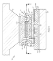
- FIG. 1 is a partial cross-sectional view of an electronic assembly including a substrate, upper and lower heatsinks, and a die package according to the present invention.
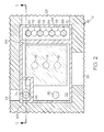
- FIG. 2 is a cross-sectional view of the electronic assembly of FIG. 1 taken along lines 2-2 of FIG. 1 .
- the reference numeral 10 generally designates an electronic assembly including an upper heatsink 12, a surface mount power transistor die package 14, a circuit board 16, and a lower heatsink 18.
- a conductor layer 20 formed on the upper face of die package 14 is thermally coupled to upper heatsink 12 with a thermal interface material 22, and set of die package terminals 24, 26, 28 formed on the lower face of die package 14 are soldered a set of conductors 30, 32, 34 formed on the upper face of circuit board 16.
- Conductor layers 36, 38 formed on the lower face of circuit board 16 are thermally coupled to lower heatsink 18 with a thermal interface material 40, and a set of metal-filled vias 42 thermally couple the upper conductor 32 to the lower conductor layer 36.
- the die package 14 is a surface-mount component that is manufactured, tested, and then mounted on the circuit board 16 as described above.
- the die package 14 includes a power FET die 50 sandwiched between an upper and lower heat conducting laminate structures 52 and 54, and a suitable under-fill material 55.
- the die package terminals 24, 26 and 28 are formed on the outboard face of lower heat conducting laminate structure 54, and are internally coupled to the gate, source and drain terminals 56, 58 and 60 of FET die 50. Since the upper and lower heat conducting laminate structures 52 and 54 are also thermally coupled to FET die 50, the die package 14 can be placed in a test fixture and tested at full power prior to its incorporation into the electronic assembly 10 of FIG. 1 .
- upper and lower heat conducting laminate structures 52, 54 each include a heat conductive but electrically insulative substrate 62, 64 of ceramic (SiN or AIN, for example) or organic material, and sets of metal (Cu or Ag, for example) conductors bonded to their upper and lower faces.
- the upper heat conductive laminate structure 52 includes the conductor layer 20 formed on the upper or outboard face of substrate 62, and a drain conductor 66 formed on the lower or inboard face of substrate 62.
- the drain conductor 66 is soldered to the drain terminal 60 of FET die 50, and the substrate 62 electrically isolates conductor layer 20 (and therefore heatsink 12) from the FET die 50.
- the lower heat conductive laminate structure 54 includes the die package terminals 24, 26 and 28 formed on the lower or outboard face of substrate 64, and gate, source and drain conductors 68, 70 and 72 formed on the upper or inboard face of substrate 64.
- the gate conductor 68 is thermally and electrically coupled to the die package terminal 24 by a metal filled via 74 through substrate 64;
- the source conductor 70 is thermally and electrically coupled to the die package terminal 26 by a set of three metal filled vias 76 through substrate 64;
- the drain conductor 72 is thermally and electrically coupled to the die package terminal 28 by a set of three metal filled vias 78 through substrate 64.
- the circuit board 16 electrically isolates the die package terminals 24 and 28 (i.e., the FET gate and drain) from heatsink 18; and the metal filled vias 42 and circuit board conductors 32 and 36 thermally couple the die package terminal 26 (i.e., the FET source) to heatsink 18.
- the upper and lower heat conducting laminate structures 52 and 54 are joined by a set of conductive standoffs 80-90 distributed about the lateral periphery of FET die 50.
- the standoffs 80-90 are integral with conductors formed on the inboard face of the upper heat conducting laminate structure 52, and are soldered to conductors formed on the inboard face of lower heat conducting laminate structure 54, but the opposite configuration is also possible.
- the standoffs 80-90 may be constructed, for example, by brazing copper balls onto a copper conductor, but other techniques are also possible.
- standoffs 80, 82, 84 and 86 extend between the drain conductor 66 of upper heat conducting laminate structure 52 and the drain conductor 72 of lower heat conducting laminate structure 54, and serve (along with vias 78) to electrically couple the FET drain terminal 60 to the die package terminal 28.
- the remaining standoffs 88 and 90 provide mechanical support between the heat conducting laminate structures 52 and 54, but serve no electrical function.
- the standoff 88 extends between the gate conductor 68 of lower heat conducting laminate structure 54 and a conductor 92 formed on the inboard face of upper substrate 62.
- the standoff 90 extends between the source conductor 70 of lower heat conducting laminate structure 54 and a conductor (not shown) formed on the inboard face of upper substrate 62.
- the above-described die package 14 and electronic assembly 10 offer many operating advantages, the foremost of which are significantly improve heat dissipation and full power testability. While the invention has been described with respect to the illustrated embodiment, it is recognized that numerous modifications and variations in addition to those mentioned herein will occur to those skilled in the art.
- the die 50 may be a device other than a FET, more or fewer standoffs may be used, the under-fill material 55 may be eliminated or replaced with a plastic molding compound, and so forth. Accordingly, it is intended that the invention not be limited to the disclosed embodiment, but that it have the full scope permitted by the language of the following claims.
Landscapes
- Cooling Or The Like Of Semiconductors Or Solid State Devices (AREA)
Abstract
Description
- The present invention relates to a surface mount electronic component including a power semiconductor die that is testable at full power and configured for both top-side and bottom-side cooling.
- High power transistor and diode semiconductor die configured for direct mounting on a substrate typically include terminal pads on both major faces. For example, a power field effect transistor (FET) has its source and gate terminals formed on one face, and its drain terminal formed on the opposite face. The terminals on one face of the die interface directly with conductors formed on the surface of a substrate on which the die is mounted, and the terminal(s) on the exposed face of the die can be coupled to other substrate conductors by wire bonding. However, the wire bonds interfere with top-side cooling of the die, effectively limiting the power dissipation of the device. The
U.S. Patent No. 6,873,043 discloses an improved arrangement in which a heat conducting laminate structure couples terminal(s) on the exposed face of the die to substrate conductors and at the same time thermally couples the die to a top-side heatsink for improved heat dissipation. - The present invention is directed to an improved packaging arrangement for a power semiconductor die in which the die is sandwiched between upper and lower heat conducting laminate structures to form a surface mount component that is configured for double-sided cooling. The upper heat conducting laminate structure electrically couples top-side die terminal(s) to conductors formed on the inboard face of the lower heat conducting laminate structure, and all of the die terminals are electrically coupled to conductors formed on the outboard face of the lower heat conducting laminate structure. As a surface mount component, the die package can be placed in a test fixture for full power testing since the upper and lower heat conducting laminate structures both protect the die and thermally couple it to the test fixture. And when the die package is installed in an electronic assembly including a substrate and upper and lower heatsinks, the die is thermally coupled to the upper heatsink through the upper heat conducting laminate structure, and to the lower heatsink through the substrate and the lower heat conducting laminate structure.
-
FIG. 1 is a partial cross-sectional view of an electronic assembly including a substrate, upper and lower heatsinks, and a die package according to the present invention. -
FIG. 2 is a cross-sectional view of the electronic assembly ofFIG. 1 taken along lines 2-2 ofFIG. 1 . - Referring to the drawings, and particularly to
FIG. 1 , thereference numeral 10 generally designates an electronic assembly including anupper heatsink 12, a surface mount powertransistor die package 14, acircuit board 16, and alower heatsink 18. Aconductor layer 20 formed on the upper face of diepackage 14 is thermally coupled toupper heatsink 12 with athermal interface material 22, and set ofdie package terminals package 14 are soldered a set ofconductors circuit board 16.Conductor layers circuit board 16 are thermally coupled tolower heatsink 18 with athermal interface material 40, and a set of metal-filledvias 42 thermally couple theupper conductor 32 to thelower conductor layer 36. - The die
package 14 is a surface-mount component that is manufactured, tested, and then mounted on thecircuit board 16 as described above. In the illustrated embodiment, the diepackage 14 includes a power FET die 50 sandwiched between an upper and lower heat conductinglaminate structures 52 and 54, and a suitable under-fill material 55. The diepackage terminals laminate structure 54, and are internally coupled to the gate, source anddrain terminals FET die 50. Since the upper and lower heat conductinglaminate structures 52 and 54 are also thermally coupled toFET die 50, thedie package 14 can be placed in a test fixture and tested at full power prior to its incorporation into theelectronic assembly 10 ofFIG. 1 . - Referring to
FIGS. 1 and2 , upper and lower heat conductinglaminate structures 52, 54 each include a heat conductive but electricallyinsulative substrate conductor layer 20 formed on the upper or outboard face ofsubstrate 62, and adrain conductor 66 formed on the lower or inboard face ofsubstrate 62. Thedrain conductor 66 is soldered to thedrain terminal 60 ofFET die 50, and thesubstrate 62 electrically isolates conductor layer 20 (and therefore heatsink 12) from theFET die 50. The lower heatconductive laminate structure 54 includes thedie package terminals substrate 64, and gate, source anddrain conductors substrate 64. Thegate conductor 68 is thermally and electrically coupled to thedie package terminal 24 by a metal filled via 74 throughsubstrate 64; thesource conductor 70 is thermally and electrically coupled to thedie package terminal 26 by a set of three metal filledvias 76 throughsubstrate 64; and thedrain conductor 72 is thermally and electrically coupled to thedie package terminal 28 by a set of three metal filledvias 78 throughsubstrate 64. In theelectronic assembly 10, thecircuit board 16 electrically isolates thedie package terminals 24 and 28 (i.e., the FET gate and drain) fromheatsink 18; and the metal filledvias 42 andcircuit board conductors - As seen in
FIGS. 1-2 , the upper and lower heat conductinglaminate structures 52 and 54 are joined by a set of conductive standoffs 80-90 distributed about the lateral periphery ofFET die 50. In the illustrated embodiment, the standoffs 80-90 are integral with conductors formed on the inboard face of the upper heat conducting laminate structure 52, and are soldered to conductors formed on the inboard face of lower heat conductinglaminate structure 54, but the opposite configuration is also possible. The standoffs 80-90 may be constructed, for example, by brazing copper balls onto a copper conductor, but other techniques are also possible. Fourstandoffs drain conductor 66 of upper heat conducting laminate structure 52 and thedrain conductor 72 of lower heat conductinglaminate structure 54, and serve (along with vias 78) to electrically couple theFET drain terminal 60 to thedie package terminal 28. Theremaining standoffs laminate structures 52 and 54, but serve no electrical function. Thestandoff 88 extends between thegate conductor 68 of lower heat conductinglaminate structure 54 and aconductor 92 formed on the inboard face ofupper substrate 62. And thestandoff 90 extends between thesource conductor 70 of lower heat conductinglaminate structure 54 and a conductor (not shown) formed on the inboard face ofupper substrate 62. - The above-described die
package 14 andelectronic assembly 10 offer many operating advantages, the foremost of which are significantly improve heat dissipation and full power testability. While the invention has been described with respect to the illustrated embodiment, it is recognized that numerous modifications and variations in addition to those mentioned herein will occur to those skilled in the art. For example, the die 50 may be a device other than a FET, more or fewer standoffs may be used, the under-fill material 55 may be eliminated or replaced with a plastic molding compound, and so forth. Accordingly, it is intended that the invention not be limited to the disclosed embodiment, but that it have the full scope permitted by the language of the following claims.
Claims (8)
- A packaging arrangement for a power semiconductor die (50) having first and second oppositely disposed major faces and one or more terminals (56/58, 60) formed on each of said major faces, comprising:a first laminate structure (54) coupled to said first face of said die (50), the first laminate structure (54) including a first substrate (64) that is heat conductive but electrically insulative, a first inboard conductor (68/70) formed on an inboard face of the first substrate (64) and electrically coupled to a terminal (56/58) on the first major surface of said die (50), a second inboard conductor (72) formed on the inboard face of the first substrate (64) laterally outboard of said die (50), first and second die package terminals (24/26, 28) formed on an outboard face of the first substrate (64) opposite said first and second inboard conductors (68/70, 72), and conductive vias (74/76, 78) through said first substrate (64) electrically coupling said first inboard conductor (68/70) to said first die package terminal (24/26) and said second inboard conductor (72) to said second die package terminal (28); anda second laminate structure (52) coupled to said second face of said die (50), the second laminate structure (52) including a second substrate (62) that is heat conductive but electrically insulative, an inboard conductor (66) formed on an inboard face of the second substrate (62) and electrically coupled to a terminal (60) on the second major surface of said die (50), and a conductive interconnect (80) electrically coupling the inboard conductor (66) of said second laminate structure (52) to the second inboard conductor (72) of said first laminate structure (54).
- The surface mount die package of claim 1, where:said inboard conductor (66) of said second laminate structure (52) extends laterally outboard of said die (50); andsaid conductive interconnect includes a conductive column (80) disposed laterally outboard of said die (50) extending between the inboard conductor (66) of said second laminate structure (52) and the second inboard conductor (72) of said first laminate structure (54).
- The surface mount die package of claim 2, where:said conductive column (80) is integral with the inboard conductor (66) of said second laminate structure (52).
- The surface mount die package of claim 2, where:said conductive column (80) is integral with the second inboard conductor (72) of said first laminate structure (54).
- The surface mount die package of claim 1, where:an outboard conductor layer (20) formed on an outboard face of said second substrate (62);a heatsink (12); anda thermally conductive material (22) thermally coupling said heatsink (12) to said outboard conductor layer (22) to dissipate heat produced by said die (50).
- The surface mount die package of claim 1, where:said first and second die package terminals (24/26, 28) on the outboard face of said first substrate (64) are soldered to conductors (30/32, 34) formed on a circuit board (16); andat least one of the circuit board conductors (32) is thermally coupled (42) to a heatsink (18) to dissipate heat produced by said die (50).
- A packaging arrangement for a power semiconductor die (50) having first and second oppositely disposed major faces, a first terminal (60) formed on said first major face and a second terminal (56/58) formed on said second major face, the packaging arrangement comprising:first and second heat conducting laminate structures (52, 54) oppositely disposed about said die (50) and having first and second inboard conductors (66, 68/70) coupled to the first and second terminals of said die (60, 56/58), where the first heat conducting laminate structure (52) electrically couples the first terminal (60) of said die (50) to a third inboard conductor (72) of said second heat conducting laminate structure (54), and said second and third inboard conductors (68/70, 72) are electrically coupled to package terminals (24/26, 28) formed on an outboard face of the second heat conducting laminate structure (54).
- The surface mount die package of claim 7, where:said die (50) is thermally coupled to a first heatsink (12) through said first heat conducting laminate structure (52), and to a second heatsink (18) through a circuit board (16) and said second heat conducting laminate structure (54).
Applications Claiming Priority (1)
| Application Number | Priority Date | Filing Date | Title |
|---|---|---|---|
| US11/983,247 US7564128B2 (en) | 2007-11-08 | 2007-11-08 | Fully testable surface mount die package configured for two-sided cooling |
Publications (2)
| Publication Number | Publication Date |
|---|---|
| EP2058860A2 true EP2058860A2 (en) | 2009-05-13 |
| EP2058860A3 EP2058860A3 (en) | 2011-03-23 |
Family
ID=40380070
Family Applications (1)
| Application Number | Title | Priority Date | Filing Date |
|---|---|---|---|
| EP08167416A Withdrawn EP2058860A3 (en) | 2007-11-08 | 2008-10-23 | Fully testable surface mount die package configured for two-sided cooling |
Country Status (2)
| Country | Link |
|---|---|
| US (1) | US7564128B2 (en) |
| EP (1) | EP2058860A3 (en) |
Cited By (2)
| Publication number | Priority date | Publication date | Assignee | Title |
|---|---|---|---|---|
| AT514085A4 (en) * | 2013-06-11 | 2014-10-15 | Austria Tech & System Tech | power module |
| CN110326105A (en) * | 2016-12-12 | 2019-10-11 | 维迪科研究所 | Method and electronic power module for integrating power chips |
Families Citing this family (3)
| Publication number | Priority date | Publication date | Assignee | Title |
|---|---|---|---|---|
| CN101568247B (en) * | 2008-04-25 | 2012-09-05 | 深圳迈瑞生物医疗电子股份有限公司 | Shielding insulating radiating system |
| CA2978795A1 (en) | 2015-03-16 | 2016-09-22 | Dana Canada Corporation | Heat exchangers with plates having surface patterns for enhancing flatness and methods for manufacturing same |
| KR101905995B1 (en) | 2016-11-09 | 2018-10-10 | 현대자동차주식회사 | Power module of double-faced cooling |
Citations (1)
| Publication number | Priority date | Publication date | Assignee | Title |
|---|---|---|---|---|
| US6873043B2 (en) | 2003-03-10 | 2005-03-29 | Delphi Technologies, Inc. | Electronic assembly having electrically-isolated heat-conductive structure |
Family Cites Families (2)
| Publication number | Priority date | Publication date | Assignee | Title |
|---|---|---|---|---|
| US6180881B1 (en) * | 1998-05-05 | 2001-01-30 | Harlan Ruben Isaak | Chip stack and method of making same |
| US7030317B1 (en) | 2005-04-13 | 2006-04-18 | Delphi Technologies, Inc. | Electronic assembly with stacked integrated circuit die |
-
2007
- 2007-11-08 US US11/983,247 patent/US7564128B2/en active Active
-
2008
- 2008-10-23 EP EP08167416A patent/EP2058860A3/en not_active Withdrawn
Patent Citations (1)
| Publication number | Priority date | Publication date | Assignee | Title |
|---|---|---|---|---|
| US6873043B2 (en) | 2003-03-10 | 2005-03-29 | Delphi Technologies, Inc. | Electronic assembly having electrically-isolated heat-conductive structure |
Cited By (3)
| Publication number | Priority date | Publication date | Assignee | Title |
|---|---|---|---|---|
| AT514085A4 (en) * | 2013-06-11 | 2014-10-15 | Austria Tech & System Tech | power module |
| AT514085B1 (en) * | 2013-06-11 | 2014-10-15 | Austria Tech & System Tech | power module |
| CN110326105A (en) * | 2016-12-12 | 2019-10-11 | 维迪科研究所 | Method and electronic power module for integrating power chips |
Also Published As
| Publication number | Publication date |
|---|---|
| US7564128B2 (en) | 2009-07-21 |
| EP2058860A3 (en) | 2011-03-23 |
| US20090121340A1 (en) | 2009-05-14 |
Similar Documents
| Publication | Publication Date | Title |
|---|---|---|
| CN101292360B (en) | Integrated circuit mounting for thermal stress relief usable in multi-chip modules | |
| US7656015B2 (en) | Packaging substrate having heat-dissipating structure | |
| US6677672B2 (en) | Structure and method of forming a multiple leadframe semiconductor device | |
| US9202798B2 (en) | Power module package and method for manufacturing the same | |
| US10490473B2 (en) | Chip package module and circuit board structure comprising the same | |
| US8451621B2 (en) | Semiconductor component and method of manufacture | |
| US7872869B2 (en) | Electronic chip module | |
| US8916958B2 (en) | Semiconductor package with multiple chips and substrate in metal cap | |
| EP3310140B1 (en) | Mounting assembly with a heatsink | |
| US20150359107A1 (en) | Electronic module with a plastic-coated electronic circuit and method for the production thereof | |
| US6809416B1 (en) | Package for integrated circuit with thermal vias and method thereof | |
| KR20090056594A (en) | Semiconductor power module package with temperature sensing element and its manufacturing method | |
| US20240114614A1 (en) | Thermal Conduction - Electrical Conduction Isolated Circuit Board with Ceramic Substrate and Power Transistor Embedded | |
| US20160086870A1 (en) | Semiconductor device | |
| CN102468249A (en) | Power encapsulation module and method for manufacturing the power encapsulation module | |
| EP1796163B1 (en) | Semiconductor device and electronic control unit using the same | |
| CN101258609B (en) | Vertical electronics packaging structure using wires arranged on laminated boards | |
| KR20190095998A (en) | Power semiconductor module | |
| KR101343199B1 (en) | Semiconductor device package | |
| KR101008772B1 (en) | Integrated circuit devices, electronic circuit support boards and thermal connections between integrated circuits and heat sinks | |
| US7564128B2 (en) | Fully testable surface mount die package configured for two-sided cooling | |
| CN101322450B (en) | IC package with internal heat dissipation structure | |
| US6483706B2 (en) | Heat dissipation for electronic components | |
| CN113206049B (en) | Semiconductor devices | |
| US7310224B2 (en) | Electronic apparatus with thermal module |
Legal Events
| Date | Code | Title | Description |
|---|---|---|---|
| PUAI | Public reference made under article 153(3) epc to a published international application that has entered the european phase |
Free format text: ORIGINAL CODE: 0009012 |
|
| AK | Designated contracting states |
Kind code of ref document: A2 Designated state(s): AT BE BG CH CY CZ DE DK EE ES FI FR GB GR HR HU IE IS IT LI LT LU LV MC MT NL NO PL PT RO SE SI SK TR |
|
| AX | Request for extension of the european patent |
Extension state: AL BA MK RS |
|
| PUAL | Search report despatched |
Free format text: ORIGINAL CODE: 0009013 |
|
| AK | Designated contracting states |
Kind code of ref document: A3 Designated state(s): AT BE BG CH CY CZ DE DK EE ES FI FR GB GR HR HU IE IS IT LI LT LU LV MC MT NL NO PL PT RO SE SI SK TR |
|
| AX | Request for extension of the european patent |
Extension state: AL BA MK RS |
|
| AKY | No designation fees paid | ||
| REG | Reference to a national code |
Ref country code: DE Ref legal event code: R108 |
|
| REG | Reference to a national code |
Ref country code: DE Ref legal event code: R108 Effective date: 20111130 |
|
| STAA | Information on the status of an ep patent application or granted ep patent |
Free format text: STATUS: THE APPLICATION IS DEEMED TO BE WITHDRAWN |
|
| 18D | Application deemed to be withdrawn |
Effective date: 20110924 |