EP2056458A2 - Radiation hardened logic circuits - Google Patents
Radiation hardened logic circuits Download PDFInfo
- Publication number
- EP2056458A2 EP2056458A2 EP08167362A EP08167362A EP2056458A2 EP 2056458 A2 EP2056458 A2 EP 2056458A2 EP 08167362 A EP08167362 A EP 08167362A EP 08167362 A EP08167362 A EP 08167362A EP 2056458 A2 EP2056458 A2 EP 2056458A2
- Authority
- EP
- European Patent Office
- Prior art keywords
- pfet
- bjt
- input terminal
- output terminal
- electrical path
- Prior art date
- Legal status (The legal status is an assumption and is not a legal conclusion. Google has not performed a legal analysis and makes no representation as to the accuracy of the status listed.)
- Granted
Links
Images


Classifications
-
- H—ELECTRICITY
- H03—ELECTRONIC CIRCUITRY
- H03K—PULSE TECHNIQUE
- H03K19/00—Logic circuits, i.e. having at least two inputs acting on one output; Inverting circuits
- H03K19/007—Fail-safe circuits
-
- H—ELECTRICITY
- H03—ELECTRONIC CIRCUITRY
- H03K—PULSE TECHNIQUE
- H03K19/00—Logic circuits, i.e. having at least two inputs acting on one output; Inverting circuits
- H03K19/003—Modifications for increasing the reliability for protection
- H03K19/0033—Radiation hardening
-
- H—ELECTRICITY
- H03—ELECTRONIC CIRCUITRY
- H03K—PULSE TECHNIQUE
- H03K19/00—Logic circuits, i.e. having at least two inputs acting on one output; Inverting circuits
- H03K19/003—Modifications for increasing the reliability for protection
-
- H—ELECTRICITY
- H03—ELECTRONIC CIRCUITRY
- H03K—PULSE TECHNIQUE
- H03K19/00—Logic circuits, i.e. having at least two inputs acting on one output; Inverting circuits
- H03K19/02—Logic circuits, i.e. having at least two inputs acting on one output; Inverting circuits using specified components
- H03K19/08—Logic circuits, i.e. having at least two inputs acting on one output; Inverting circuits using specified components using semiconductor devices
- H03K19/094—Logic circuits, i.e. having at least two inputs acting on one output; Inverting circuits using specified components using semiconductor devices using field-effect transistors
- H03K19/09403—Logic circuits, i.e. having at least two inputs acting on one output; Inverting circuits using specified components using semiconductor devices using field-effect transistors using junction field-effect transistors
- H03K19/09418—Logic circuits, i.e. having at least two inputs acting on one output; Inverting circuits using specified components using semiconductor devices using field-effect transistors using junction field-effect transistors in combination with bipolar transistors [BIFET]
Definitions
- This invention relates, generally, to radiation hardened logic circuits. More particularly, this invention relates to radiation hardened logic circuits that are resistant to damage caused by charges developed in the circuit after long exposure to ionizing radiation.
- Typical sources of exposure of electronics to ionizing radiation are solar wind and the Van Allen radiation belts for satellites, nuclear reactors in power plants for sensors and control circuits, residual radiation from isotopes in chip packaging materials, cosmic radiation for both high-altitude airplanes and satellites, and nuclear explosions for potentially all military and civilian electronics.
- the first known as the total ionizing dose, represents the cumulative effect of many particles hitting a device throughout the course of its mission life, slowly degrading the device until it ultimately fails.
- the second involves high-energy particles that penetrate deep into materials and components, leaving a temporary trail of free charge carriers in their wake. If these particles hit vulnerable spots in the circuit, they may produce adverse effects, described generally as single-event effects.
- CMOS complementary metal-oxide semiconductor
- the present invention provides a radiation hardened inverter including first and second electrical paths between an input terminal and an output terminal.
- a first PFET is disposed in the first electrical path, and a bipolar junction transistor (BJT) is disposed in the second electrical path.
- the first PFET is configured to convert a low level signal at the input terminal to a high level signal at the output terminal, and the BJT is configured to convert a high level signal at the input terminal to a low level signal at the output terminal.
- the radiation hardened inverter in a preferred embodiement further includes a second PFET disposed in the second electrical path. The second PFET is configured to provide a path for bleeding excess current away from the BJT.
- the radiation hardened inverter also may include a current limiting PFET disposed in the second electrical path. Such current limiting PFET is configured to limit current flowing into a base of the BJT.
- the radiation hardened inverter is free-of any NFETs.
- the first PFET includes a gate connected to the input terminal, a source connected to a voltage reference, and a drain connected to the output terminal.
- the second PFET of the preferred embodiment includes a gate connected to a ground reference, a source connected to a base of the BJT, and a drain connected to the ground reference.
- the BJT includes a collector connected to the output terminal, and an emitter connected to the ground reference.
- the current limiting PFET includes a gate connected to the ground reference, a source connected to the input terminal, and a drain connected to the base of the BJT.
- a capacitor is coupled between the second PFET and the input terminal for speeding up conversion of the low level signal at the input terminal to the high level signal at the output terminal.
- Another embodiment of the invention using the same principle of using a bipolar junction transistor (BJT) to connect the output terminal to the ground reference is a radiation hardened NAND gate having first and second electrical paths between a first input terminal and an output terminal. Third and fourth electrical paths are included between a second input terminal and the output terminal.
- the NAND gate also includes a first PFET disposed in the first electrical path, a first BJT disposed in the second electrical path, a second PFET disposed in the third electrical path, and a second BJT disposed in the fourth electrical path.
- the first and second PFETs convert a low level signal at the first or second input terminal to a high level signal at the output terminal.
- the first and second BJTs convert high level signals, respectively, at the first and second input terminals to a low level signal at the output terminal.
- the radiation hardened NAND gate in a first preferred embodiment includes a third PFET disposed in the second electrical path, and a fourth PFET disposed in the fourth electrical path. The third and fourth PFETs, respectively, bleed excess current away from the first and second BJTs.
- the radiation hardened NAND gate in a second preferred embodiment also includes first and second current limiting PFETs disposed, respectively, in the second and fourth electrical paths. The first and second current limiting PFETs are configured to limit current flowing into a respective base of the first and second BJTs.
- the radiation hardened NAND gate is free-of any NFETs.
- the first PFET includes a gate connected to the first input terminal, a source connected to a voltage reference, and a drain connected to the output terminal.
- the third PFET includes a gate connected to a ground reference, a source connected to a base of the first BJT, and a drain connected to the ground reference.
- the first BJT includes a collector connected to the output terminal, and an emitter connected to a collector of the second BJT.
- the second PFET includes a gate connected to the second input terminal, a source connected to the voltage reference, and a drain connected to the output terminal.
- the fourth PFET includes a gate connected to the ground reference, a source connected to a base of the second BJT, and a drain connected to the ground reference.
- the second BJT includes an emitter connected to the ground reference.
- a first current limiting PFET is disposed in the second electrical path.
- the first current limiting PFET includes a gate connected to the ground reference, a source connected to the first input terminal, and a drain connected to the base of the first BJT.
- a second current limiting PFET is disposed in the fourth electrical path.
- the second current limiting PFET includes a gate connected to the ground reference, a source connected to the second input terminal, and a drain connected to the base of the second BJT.
- a first capacitor is coupled between the third PFET and the first input terminal for speeding up conversion of the low level signal at the first input terminal to the high level signal at the output terminal.
- a second capacitor is coupled between the fourth PFET and the second input terminal for speeding up conversion of the low level signal at the second input terminal to the high level signal at the output terminal.
- FIG. 1 shows a conventional CMOS inverter circuit including PFET 104, NFET 108, input terminal 100, output terminal 106, voltage reference 102 and ground reference 110.
- Input terminal 100 is connected to the gate of PFET 104 by way of first electrical path 111.
- Input terminal 100 is also connected to the gate of NFET 108 by way of second electrical path 112.
- the drain of PFET 104 and the source of NFET 108 are connected to output terminal 106.
- the source of PFET 104 is connected to voltage reference 102 and, in addition, the drain of NFET 108 is connected to ground reference 110.
- CMOS inverter circuit 120 produces an output signal that is complimentary to its input signal.
- PFET 104 is turned off and NFET 108 is turned on. Because PFET 104 is turned off, voltage reference 102 is not applied to output terminal 106. Because NFET 108 is turned on, ground reference 110 is applied to output terminal 106, thereby providing a logic 0 output signal.
- PFET 104 is turned on and NFET 108 is turned off. Because NFET 108 is turned off, ground reference 110 is not applied to output terminal 106. Because PFET 104 is turned on, voltage reference 102 is applied to output terminal 106, thereby providing a logic 1 output signal.
- FIG. 2 shows a conventional CMOS NAND circuit 220 including PFET 206, PFET 208, NFET 212, NFET 214, input terminal 202, input terminal 204, output terminal 210, voltage reference 200, and ground reference 216.
- Input terminal 202 is connected to the gate of PFET 206 by way of first electrical path 221.
- Input terminal 202 is also connected to the gate of NFET 212 by way of second electrical path 222.
- Input terminal 204 is connected to the gate of PFET 208 by way of third electrical path 223.
- Input terminal 204 is also connected to the gate of NFET 214 by way of fourth electrical path 224.
- Voltage reference 200 is connected to the sources of PFET 206 and PFET 208.
- Output terminal 210 is connected to the drains of PFET 206 and PFET 208 and the source of NFET 212.
- the drain of NFET 212 is connected to the source of NFET 214.
- the drain of NFET 214 is connected to ground reference 216.
- a NAND circuit produces a logic 0 output signal, when both input signals are a logic 1. Any other possible input signal levels produce a logic 1 output signal. More, specifically, when a logic 0 input signal is applied to input terminals 202 and 204, both PFET 206 and PFET 208 are turned on and both NFET 212 and NFET 214 are turned off. With both PFET 206 and PFET 208 turned on, voltage reference 200 is applied to output terminal 210, thereby providing a logic 1 output signal.
- both PFET 206 and NFET 214 are turned off, and both PFET 208 and NFET 212 are turned on.
- voltage reference 200 is applied to output terminal 210, thereby providing a logic 1 output signal.
- both PFET 206 and PFET 208 are turned off and both NFET 212 and NFET 214 are turned on.
- ground reference 216 is applied to output terminal 210, thereby providing a logic 0 output signal.
- CMOS inverter circuit 120 and CMOS NAND circuit 220 include NFET components, they are susceptible to failure from long term radiation.
- BJT bipolar junction transistor
- a logic circuit becomes more radiation hardened. Since a logic circuit includes combinations of one or more inverter circuits and/or one or more NAND circuits, any logic circuit may be formed to provide a desired logical function. More importantly, any logic circuit may be radiation hardened using embodiments of the invention described below.
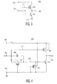
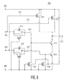
- FIGS. 3 and 5 depict basic inverter and NAND circuits, respectively, that are radiation hardened, because all NFET components in the CMOS circuits have been eliminated.
- FIGS. 4 and 6 show components added to the basic inverter and NAND circuits, respectively. As will be explained, these additional components provide operational improvements to the basic logic circuits depicted in FIGS. 3 and 5 .
- Hybrid inverter circuit 320 includes PFET 304, BJT 308, input terminal 302, output terminal 306, voltage reference 300 and ground reference 310.
- Voltage reference 300 is connected to the source of PFET 304.
- Input terminal 302 is connected to the gate of PFET 304 by way of first electrical path 311, and connected to the base of BJT 308 by way of second electrical path 312.
- Output terminal 306 is connected to the drain of PFET 304 and the collector of BJT 308. Furthermore, the emitter of BJT 308 is connected to ground reference 310.
- Hybrid inverter circuit 320 produces an output signal that is complimentary to its input signal.
- PFET 304 is turned off and BJT 308 is turned on. Because PFET 304 is turned off, voltage reference 300 is not applied to output terminal 306. Because BJT 308 is turned on, ground reference 310 is applied to output terminal 306, thereby providing a logic 0 output signal.
- PFET 304 is turned on and BJT 308 is turned off. Because BJT 308 is turned off, ground reference 310 is not applied to output terminal 306. Because PFET 304 is turned on, voltage reference 300 is applied to output terminal 306, thereby providing a logic 1 output signal.
- Hybrid inverter circuit 420 includes components that are identical to the inverter circuit shown in FIG. 3 and additional components which improve the circuit operation. As shown, hybrid inverter circuit 420 includes first PFET 406, second PFET 416, current limiting PFET 408, BJT 412, input terminal 402, output terminal 414, capacitor 404, voltage reference 400 and ground reference 410.
- Voltage reference 400 is connected to the source and substrate of first PFET 406 and the substrate of second PFET 416.
- Input terminal 402 is connected to the gate of first PFET 406 by way of first electrical path 421.
- Input terminal 402 is also coupled to the base of BJT 412 by way of second electrical path 422.
- input terminal 402 is connected to the source and substrate of current limiting PFET 408 and the negative terminal of capacitor 404.
- the base of BJT 412 is connected to the positive terminal of capacitor 404, the drain of current limiting PFET 408, and the source of second PFET 416.
- the gate of current limiting PFET 408, the gate and drain of second PFET 416 and the emitter of BJT 412 are connected to ground reference 410.
- Output terminal 414 is connected to the drain of first PFET 406 and the collector of BJT 412.
- hybrid inverter circuit 420 of FIG. 4 operates similarly to hybrid inverter circuit 320 of FIG. 3 .
- first PFET 406 is turned off, by way of first electrical path 421; and PFET 408 and BJT 412 are turned on. Because first PFET 406 is turned off, voltage reference 400 is not applied to output terminal 414. Because BJT 412 is turned on, ground reference 410 is applied to output terminal 414, thereby providing a logic 0 output signal.
- first PFET 406 is turned on, by way of first electrical path 421; and current limiting PFET 408 and BJT 412 are turned off. Because BJT 412 is turned off, ground reference 410 is not applied to output terminal 414. Because first PFET 406 is turned on, voltage reference 400 is applied to output terminal 414, thereby providing a logic 1 output signal.
- BJT 412 is an NPN transistor having a semiconductor channel, which is turned on and off, in response to current flowing through its base-emitter junction.
- current limiting PFET 408 is included in hybrid inverter circuit 420 to limit the current flowing into the base of BJT 412. This prevents the base current flowing into BJT 412 from exceeding a level which may damage BJT 412.
- an excessive electric charge may accumulate at the base of BJT 412.
- bleeder PFET 416 is connected to the base of BJT 412. In this manner, any accumulating electric charge flows away from the base of BJT 412, through PFET 416, toward ground reference 410. Since the gate of PFET 416 is connected to the ground reference, PFET 416 is on and is able to conduct any current from its source to its drain.
- speed up capacitor 404 is included between input terminal 402 and the base of BJT 412. During a logic state change at input terminal 402, speed up capacitor 404 provides a current spike to the base of BJT 412, thereby decreasing the interval between a logic transition time at the input terminal and the BJT turn on/off time.
- hybrid NAND circuit 520 includes PFET 506, PFET 508, BJT 512, BJT 514, input terminal 502, input terminal 504, output terminal 510, voltage reference 500, and ground reference 516.
- Input terminal 502 is connected to the gate of PFET 506 by way of first electrical path 521.
- Input terminal 502 is also connected to the base of BJT 512 by way of second electrical path 522.
- Input terminal 504 is connected to the gate of PFET 508 by way of third electrical path 523.
- Input terminal 504 is also connected to the base of BJT 514 by way of fourth electrical path 524.
- Voltage reference 500 is applied to the sources of both PFET 506 and PFET 508.
- Output terminal 510 is connected to the drain of PFET 506, the drain of PFET 508 and the collector of BJT 512.
- the emitter of BJT 512 is connected to the collector of BJT 514. Furthermore, the emitter of BJT 514 is connected to ground reference 516.
- Hybrid NAND circuit 520 provides a logic 0 output signal when both input signals are logic 1. Any other possible input signal levels provides a logic 1 output signal. More specifically, when a logic 0 input signal is applied to both input terminals 502 and 504, both PFET 506 and PFET 508 are turned on and both BJT 512 and BJT 514 are turned off. With both PFET 506 and PFET 508 turned on, voltage reference 500 is applied to output terminal 510, thereby providing a logic 1 output signal.
- both PFET 506 and BJT 514 are turned on, and both PFET 508 and BJT 512 are turned off.
- voltage reference 500 is applied to output terminal 510, thereby providing a logic 1 output signal.
- both PFET 506 and BJT 514 are turned off, and both PFET 508 and BJT 512 are turned on.
- voltage reference 500 is applied to output terminal 510, thereby providing a logic 1 output signal.
- both PFET 506 and PFET 508 are turned off and both BJT 512 and BJT 514 are turned on.
- ground reference 516 is applied to output terminal 510, thereby providing a logic 0 output signal.
- Hybrid NAND circuit 650 includes components that are identical to NAND circuit 520 shown in FIG. 5 and additional components to improve circuit operation. As shown, hybrid NAND circuit 650 includes first PFET 608, second PFET 626, third PFET 610, fourth PFET 628, current limiting PFET 616, current limiting PFET 622, first BJT 618, second BJT 624, capacitor 614, capacitor 620, input terminal 602, input terminal 604, output terminal 612, voltage reference 600 and ground reference 606.
- Input terminal 602 is connected to the gate of first PFET 608 by way of first electrical path 651, the negative terminal of capacitor 614 and the source and substrate of current limiting PFET 616.
- Input terminal 604 is connected to the gate of third PFET 610 by way of third electrical path 653, the negative terminal of capacitor 620 and the source and substrate of current limiting PFET 622.
- Voltage reference 600 is connected to the source and substrate of first PFET 608 and third PFET 610.
- Voltage reference 600 is also connected to the substrate of second PFET 626 and third PFET 628.
- Output terminal 612 is connected to the drain of first PFET 608, the drain of third PFET 610 and to the collector of first BJT 618.
- the emitter of first BJT 618 is connected to the collector of second BJT 624.
- the base of first BJT 618 is connected to the positive terminal of capacitor 614, the drain of current limiting PFET 616 and the source of second PFET 626, by way of second electrical path 652.
- the base of second BJT 624 is connected to the positive terminal of capacitor 620, the drain of current limiting PFET 622 and the source of fourth PFET 628, by way of fourth electrical path 654.
- Ground reference 606 is connected to the emitter of second BJT 624, the gate of PFET 616, the gate of PFET 622, the gate and drain of PFET 626 and the gate and drain of PFET 628.
Landscapes
- Engineering & Computer Science (AREA)
- Physics & Mathematics (AREA)
- Computer Hardware Design (AREA)
- Computing Systems (AREA)
- General Engineering & Computer Science (AREA)
- Mathematical Physics (AREA)
- Power Engineering (AREA)
- Logic Circuits (AREA)
- Metal-Oxide And Bipolar Metal-Oxide Semiconductor Integrated Circuits (AREA)
- Semiconductor Integrated Circuits (AREA)
Abstract
Description
- This invention relates, generally, to radiation hardened logic circuits. More particularly, this invention relates to radiation hardened logic circuits that are resistant to damage caused by charges developed in the circuit after long exposure to ionizing radiation.
- Environments with high levels of ionizing radiation create special design challenges. A single charged particle may knock thousands of electrons loose, causing electronic noise and signal spikes. In the case of digital circuits, this may cause results which are inaccurate or unintelligible. This is a particularly serious problem in the design of artificial satellites, spacecraft, military aircraft, nuclear power stations, and nuclear weapons. In order to ensure the proper operation of such systems, manufacturers of integrated circuits and sensors intended for the aerospace markets employ various methods of radiation hardening. The resulting systems are said to be radiation-hardened.
- Typical sources of exposure of electronics to ionizing radiation are solar wind and the Van Allen radiation belts for satellites, nuclear reactors in power plants for sensors and control circuits, residual radiation from isotopes in chip packaging materials, cosmic radiation for both high-altitude airplanes and satellites, and nuclear explosions for potentially all military and civilian electronics.
- Two types of space radiation are of particular concern for spacecraft electronics designers. The first, known as the total ionizing dose, represents the cumulative effect of many particles hitting a device throughout the course of its mission life, slowly degrading the device until it ultimately fails. The second involves high-energy particles that penetrate deep into materials and components, leaving a temporary trail of free charge carriers in their wake. If these particles hit vulnerable spots in the circuit, they may produce adverse effects, described generally as single-event effects.
- One type of electronic component often found aboard a satellite is the complementary metal-oxide semiconductor (CMOS) integrated circuit. As commercial CMOS processes have advanced, the inherent radiation resistance of these devices has improved. For example, the current that flows through CMOS transistors is governed by a low-voltage gate over each device, isolated by a layer of oxide. These insulating layers may develop a charge after long exposure to ionizing radiation, and this charge may affect the flow of current through the device. As circuits have shrunk, however, the thicknesses of these insulating layers have decreased, presenting less opportunity for charge buildup.
- More problematic are the radiation-induced increases in leakage current. Leakage also increases the amount of current flowing in the circuit, when the device is in a quiescent state. Such an increase, multiplied by the tens of millions of switches in each circuit, may drive up power consumption. In an extreme case, the isolation between discrete components may also be lost, rendering the circuit useless.
- To meet this and other needs, and in view of its purposes, the present invention provides a radiation hardened inverter including first and second electrical paths between an input terminal and an output terminal. A first PFET is disposed in the first electrical path, and a bipolar junction transistor (BJT) is disposed in the second electrical path. The first PFET is configured to convert a low level signal at the input terminal to a high level signal at the output terminal, and the BJT is configured to convert a high level signal at the input terminal to a low level signal at the output terminal. The radiation hardened inverter in a preferred embodiement further includes a second PFET disposed in the second electrical path. The second PFET is configured to provide a path for bleeding excess current away from the BJT. The radiation hardened inverter also may include a current limiting PFET disposed in the second electrical path. Such current limiting PFET is configured to limit current flowing into a base of the BJT. The radiation hardened inverter is free-of any NFETs.
- The first PFET includes a gate connected to the input terminal, a source connected to a voltage reference, and a drain connected to the output terminal. The second PFET of the preferred embodiment includes a gate connected to a ground reference, a source connected to a base of the BJT, and a drain connected to the ground reference. The BJT includes a collector connected to the output terminal, and an emitter connected to the ground reference. The current limiting PFET includes a gate connected to the ground reference, a source connected to the input terminal, and a drain connected to the base of the BJT. In a further preferred embodiment a capacitor is coupled between the second PFET and the input terminal for speeding up conversion of the low level signal at the input terminal to the high level signal at the output terminal.
- Another embodiment of the invention using the same principle of using a bipolar junction transistor (BJT) to connect the output terminal to the ground reference is a radiation hardened NAND gate having first and second electrical paths between a first input terminal and an output terminal. Third and fourth electrical paths are included between a second input terminal and the output terminal. The NAND gate also includes a first PFET disposed in the first electrical path, a first BJT disposed in the second electrical path, a second PFET disposed in the third electrical path, and a second BJT disposed in the fourth electrical path. The first and second PFETs convert a low level signal at the first or second input terminal to a high level signal at the output terminal. The first and second BJTs convert high level signals, respectively, at the first and second input terminals to a low level signal at the output terminal. The radiation hardened NAND gate in a first preferred embodiment includes a third PFET disposed in the second electrical path, and a fourth PFET disposed in the fourth electrical path. The third and fourth PFETs, respectively, bleed excess current away from the first and second BJTs. The radiation hardened NAND gate in a second preferred embodiment also includes first and second current limiting PFETs disposed, respectively, in the second and fourth electrical paths. The first and second current limiting PFETs are configured to limit current flowing into a respective base of the first and second BJTs. The radiation hardened NAND gate is free-of any NFETs.
- The first PFET includes a gate connected to the first input terminal, a source connected to a voltage reference, and a drain connected to the output terminal. The third PFET includes a gate connected to a ground reference, a source connected to a base of the first BJT, and a drain connected to the ground reference. The first BJT includes a collector connected to the output terminal, and an emitter connected to a collector of the second BJT. The second PFET includes a gate connected to the second input terminal, a source connected to the voltage reference, and a drain connected to the output terminal. The fourth PFET includes a gate connected to the ground reference, a source connected to a base of the second BJT, and a drain connected to the ground reference. The second BJT includes an emitter connected to the ground reference. A first current limiting PFET is disposed in the second electrical path. The first current limiting PFET includes a gate connected to the ground reference, a source connected to the first input terminal, and a drain connected to the base of the first BJT. A second current limiting PFET is disposed in the fourth electrical path. The second current limiting PFET includes a gate connected to the ground reference, a source connected to the second input terminal, and a drain connected to the base of the second BJT. In a further preferred embodiment a first capacitor is coupled between the third PFET and the first input terminal for speeding up conversion of the low level signal at the first input terminal to the high level signal at the output terminal. A second capacitor is coupled between the fourth PFET and the second input terminal for speeding up conversion of the low level signal at the second input terminal to the high level signal at the output terminal.
- It is understood that the foregoing general description and the following detailed description are exemplary, but are not restrictive, of the invention.
- The invention is best understood from the following detailed description when read in connection with the accompanying drawing. Included in the drawing are the following figures:
- FIG. 1
- is a conventional inverter circuit.
- FIG. 2
- is a conventional NAND gate circuit.
- FIG. 3
- is a radiation hardened inverter circuit, in accordance with an embodiment of the present invention.
- FIG. 4
- is another radiation hardened inverter circuit, in accordance with an embodiment of the present invention.
- FIG. 5
- is a radiation hardened NAND gate circuit, in accordance with an embodiment of the present invention.
- FIG. 6
- is another radiation hardened NAND gate circuit, in accordance with an embodiment of the present invention.
-
FIG. 1 shows a conventional CMOS invertercircuit including PFET 104,NFET 108,input terminal 100,output terminal 106,voltage reference 102 andground reference 110.Input terminal 100 is connected to the gate ofPFET 104 by way of firstelectrical path 111.Input terminal 100 is also connected to the gate ofNFET 108 by way of secondelectrical path 112. The drain ofPFET 104 and the source ofNFET 108 are connected tooutput terminal 106. Furthermore, the source ofPFET 104 is connected tovoltage reference 102 and, in addition, the drain ofNFET 108 is connected to groundreference 110. - Operation of
CMOS inverter circuit 120 will now be described. In general, an inverter circuit produces an output signal that is complimentary to its input signal. In operation, when a logic 1 input signal is applied to input terminal 100,PFET 104 is turned off andNFET 108 is turned on. BecausePFET 104 is turned off,voltage reference 102 is not applied tooutput terminal 106. BecauseNFET 108 is turned on,ground reference 110 is applied tooutput terminal 106, thereby providing a logic 0 output signal. When a logic 0 input signal is applied to input terminal 100,PFET 104 is turned on andNFET 108 is turned off. BecauseNFET 108 is turned off,ground reference 110 is not applied tooutput terminal 106. BecausePFET 104 is turned on,voltage reference 102 is applied tooutput terminal 106, thereby providing a logic 1 output signal. -
FIG. 2 shows a conventionalCMOS NAND circuit 220 includingPFET 206, PFET 208,NFET 212, NFET 214,input terminal 202,input terminal 204,output terminal 210,voltage reference 200, andground reference 216.Input terminal 202 is connected to the gate ofPFET 206 by way of firstelectrical path 221.Input terminal 202 is also connected to the gate ofNFET 212 by way of secondelectrical path 222.Input terminal 204 is connected to the gate of PFET 208 by way of thirdelectrical path 223.Input terminal 204 is also connected to the gate of NFET 214 by way of fourthelectrical path 224.Voltage reference 200 is connected to the sources ofPFET 206 and PFET 208.Output terminal 210 is connected to the drains ofPFET 206 and PFET 208 and the source ofNFET 212. The drain ofNFET 212 is connected to the source of NFET 214. Furthermore, the drain of NFET 214 is connected to groundreference 216. - Operation of the standard
CMOS NAND circuit 220 will now be described. In general, a NAND circuit produces a logic 0 output signal, when both input signals are a logic 1. Any other possible input signal levels produce a logic 1 output signal. More, specifically, when a logic 0 input signal is applied to inputterminals PFET 206 and PFET 208 are turned on and bothNFET 212 and NFET 214 are turned off. With bothPFET 206 and PFET 208 turned on,voltage reference 200 is applied tooutput terminal 210, thereby providing a logic 1 output signal. On the other hand, when a logic 0 input signal is applied to input terminal 202 and a logic 1 input signal is applied to input terminal 204, bothPFET 206 and NFET 214 are turned on, and both PFET 208 andNFET 212 are turned off. WithPFET 206 turned on,voltage reference 200 is applied tooutput terminal 210, thereby providing a logic 1 output signal. - Similarly, when a logic 1 input signal is applied to input terminal 202 and a logic 0 input signal is applied to input terminal 204, both
PFET 206 and NFET 214 are turned off, and both PFET 208 andNFET 212 are turned on. With PFET 208 turned on,voltage reference 200 is applied tooutput terminal 210, thereby providing a logic 1 output signal. On the other hand, when a logic 1 input signal is applied to bothinput terminal 202 andinput terminal 204, bothPFET 206 and PFET 208 are turned off and bothNFET 212 and NFET 214 are turned on. With bothNFET 206 and NFET 208 turned on,ground reference 216 is applied tooutput terminal 210, thereby providing a logic 0 output signal. - Because
CMOS inverter circuit 120 andCMOS NAND circuit 220 include NFET components, they are susceptible to failure from long term radiation. The inventor has discovered that by replacing all NFET components with bipolar junction transistor (BJT) components, a logic circuit becomes more radiation hardened. Since a logic circuit includes combinations of one or more inverter circuits and/or one or more NAND circuits, any logic circuit may be formed to provide a desired logical function. More importantly, any logic circuit may be radiation hardened using embodiments of the invention described below. - The following provides a description of the building blocks of a logic circuit, namely an inverter circuit and a NAND circuit, which are radiation hardened, in accordance with the present invention. The description refers to
FIGS. 3 and5 , which depict basic inverter and NAND circuits, respectively, that are radiation hardened, because all NFET components in the CMOS circuits have been eliminated. Furthermore, the description refers toFIGS. 4 and6 , which show components added to the basic inverter and NAND circuits, respectively. As will be explained, these additional components provide operational improvements to the basic logic circuits depicted inFIGS. 3 and5 . - Referring first to
FIG. 3 , there is shown a hybrid inverter circuit, generally designated as 320, whereNFET 108 ofFIG. 1 has been replaced withBJT 308.Hybrid inverter circuit 320 includesPFET 304,BJT 308,input terminal 302,output terminal 306,voltage reference 300 andground reference 310.Voltage reference 300 is connected to the source ofPFET 304.Input terminal 302 is connected to the gate ofPFET 304 by way of firstelectrical path 311, and connected to the base ofBJT 308 by way of secondelectrical path 312.Output terminal 306 is connected to the drain ofPFET 304 and the collector ofBJT 308. Furthermore, the emitter ofBJT 308 is connected to groundreference 310. - Operation of
hybrid inverter circuit 320 will now be described.Hybrid inverter circuit 320 produces an output signal that is complimentary to its input signal. In operation, when a logic 1 input signal is applied to input terminal 302,PFET 304 is turned off andBJT 308 is turned on. BecausePFET 304 is turned off,voltage reference 300 is not applied tooutput terminal 306. BecauseBJT 308 is turned on,ground reference 310 is applied tooutput terminal 306, thereby providing a logic 0 output signal. On the other hand, when a logic 0 input signal is applied to input terminal 302,PFET 304 is turned on andBJT 308 is turned off. BecauseBJT 308 is turned off,ground reference 310 is not applied tooutput terminal 306. BecausePFET 304 is turned on,voltage reference 300 is applied tooutput terminal 306, thereby providing a logic 1 output signal. - Referring next to
FIG. 4 , there is shown another hybrid inverter circuit, generally designated as 420.Hybrid inverter circuit 420 includes components that are identical to the inverter circuit shown inFIG. 3 and additional components which improve the circuit operation. As shown,hybrid inverter circuit 420 includesfirst PFET 406,second PFET 416, current limitingPFET 408,BJT 412,input terminal 402,output terminal 414,capacitor 404,voltage reference 400 andground reference 410. -
Voltage reference 400 is connected to the source and substrate offirst PFET 406 and the substrate ofsecond PFET 416.Input terminal 402 is connected to the gate offirst PFET 406 by way of firstelectrical path 421.Input terminal 402 is also coupled to the base ofBJT 412 by way of secondelectrical path 422. Moreover,input terminal 402 is connected to the source and substrate of current limitingPFET 408 and the negative terminal ofcapacitor 404. The base ofBJT 412 is connected to the positive terminal ofcapacitor 404, the drain of current limitingPFET 408, and the source ofsecond PFET 416. The gate of current limitingPFET 408, the gate and drain ofsecond PFET 416 and the emitter ofBJT 412 are connected to groundreference 410.Output terminal 414 is connected to the drain offirst PFET 406 and the collector ofBJT 412. - Except for the additional components, namely
capacitor 404 and PFETs 408 and 416,hybrid inverter circuit 420 ofFIG. 4 operates similarly tohybrid inverter circuit 320 ofFIG. 3 . In operation, when a logic 1 input signal is applied to input terminal 402,first PFET 406 is turned off, by way of firstelectrical path 421; andPFET 408 andBJT 412 are turned on. Becausefirst PFET 406 is turned off,voltage reference 400 is not applied tooutput terminal 414. BecauseBJT 412 is turned on,ground reference 410 is applied tooutput terminal 414, thereby providing a logic 0 output signal. On the other hand, when a logic 0 input signal is applied to input terminal 402,first PFET 406 is turned on, by way of firstelectrical path 421; and current limitingPFET 408 andBJT 412 are turned off. BecauseBJT 412 is turned off,ground reference 410 is not applied tooutput terminal 414. Becausefirst PFET 406 is turned on,voltage reference 400 is applied tooutput terminal 414, thereby providing a logic 1 output signal. -
BJT 412 is an NPN transistor having a semiconductor channel, which is turned on and off, in response to current flowing through its base-emitter junction. In the embodiment ofFIG. 4 , current limitingPFET 408 is included inhybrid inverter circuit 420 to limit the current flowing into the base ofBJT 412. This prevents the base current flowing intoBJT 412 from exceeding a level which may damageBJT 412. - In addition, an excessive electric charge may accumulate at the base of
BJT 412. In order to bleed away any excessive electric charge from the base ofBJT 412,bleeder PFET 416 is connected to the base ofBJT 412. In this manner, any accumulating electric charge flows away from the base ofBJT 412, throughPFET 416, towardground reference 410. Since the gate ofPFET 416 is connected to the ground reference,PFET 416 is on and is able to conduct any current from its source to its drain. - As also shown in
FIG. 4 , speed upcapacitor 404 is included betweeninput terminal 402 and the base ofBJT 412. During a logic state change atinput terminal 402, speed upcapacitor 404 provides a current spike to the base ofBJT 412, thereby decreasing the interval between a logic transition time at the input terminal and the BJT turn on/off time. - Referring next to
FIG. 5 , there is shown a hybrid NAND circuit, generally designated as 520, where both NFETs ofFIG. 2 have been replaced with two BJTs. As shown,hybrid NAND circuit 520 includesPFET 506,PFET 508,BJT 512,BJT 514,input terminal 502,input terminal 504,output terminal 510,voltage reference 500, andground reference 516.Input terminal 502 is connected to the gate ofPFET 506 by way of firstelectrical path 521.Input terminal 502 is also connected to the base ofBJT 512 by way of secondelectrical path 522.Input terminal 504 is connected to the gate ofPFET 508 by way of thirdelectrical path 523.Input terminal 504 is also connected to the base ofBJT 514 by way of fourthelectrical path 524.Voltage reference 500 is applied to the sources of bothPFET 506 andPFET 508.Output terminal 510 is connected to the drain ofPFET 506, the drain ofPFET 508 and the collector ofBJT 512. The emitter ofBJT 512 is connected to the collector ofBJT 514. Furthermore, the emitter ofBJT 514 is connected to groundreference 516. - Operation of
hybrid NAND circuit 520 will now be described.Hybrid NAND circuit 520 provides a logic 0 output signal when both input signals are logic 1. Any other possible input signal levels provides a logic 1 output signal. More specifically, when a logic 0 input signal is applied to bothinput terminals PFET 506 andPFET 508 are turned on and bothBJT 512 andBJT 514 are turned off. With bothPFET 506 andPFET 508 turned on,voltage reference 500 is applied tooutput terminal 510, thereby providing a logic 1 output signal. On the other hand, when a logic 0 input signal is applied to input terminal 502 and a logic 1 input signal is applied to input terminal 504, bothPFET 506 andBJT 514 are turned on, and bothPFET 508 andBJT 512 are turned off. WithPFET 506 turned on,voltage reference 500 is applied tooutput terminal 510, thereby providing a logic 1 output signal. - Similarly, when a logic 1 input signal is applied to input terminal 502 and a logic 0 input signal is applied to input terminal 504, both
PFET 506 andBJT 514 are turned off, and bothPFET 508 andBJT 512 are turned on. WithPFET 508 turned on,voltage reference 500 is applied tooutput terminal 510, thereby providing a logic 1 output signal. On the other hand, when a logic 1 input signal is applied to bothinput terminal 502 andinput terminal 504, bothPFET 506 andPFET 508 are turned off and bothBJT 512 andBJT 514 are turned on. With bothBJT 512 andBJT 514 turned on,ground reference 516 is applied tooutput terminal 510, thereby providing a logic 0 output signal. - Referring now to
FIG. 6 , there is shown another hybrid NAND circuit, generally designated as 650.Hybrid NAND circuit 650 includes components that are identical toNAND circuit 520 shown inFIG. 5 and additional components to improve circuit operation. As shown,hybrid NAND circuit 650 includesfirst PFET 608,second PFET 626,third PFET 610,fourth PFET 628, current limitingPFET 616, current limitingPFET 622,first BJT 618,second BJT 624,capacitor 614,capacitor 620,input terminal 602,input terminal 604,output terminal 612,voltage reference 600 andground reference 606. -
Input terminal 602 is connected to the gate offirst PFET 608 by way of firstelectrical path 651, the negative terminal ofcapacitor 614 and the source and substrate of current limitingPFET 616.Input terminal 604 is connected to the gate ofthird PFET 610 by way of thirdelectrical path 653, the negative terminal ofcapacitor 620 and the source and substrate of current limitingPFET 622.Voltage reference 600 is connected to the source and substrate offirst PFET 608 andthird PFET 610.Voltage reference 600 is also connected to the substrate ofsecond PFET 626 andthird PFET 628.Output terminal 612 is connected to the drain offirst PFET 608, the drain ofthird PFET 610 and to the collector offirst BJT 618. - The emitter of
first BJT 618 is connected to the collector ofsecond BJT 624. The base offirst BJT 618 is connected to the positive terminal ofcapacitor 614, the drain of current limitingPFET 616 and the source ofsecond PFET 626, by way of secondelectrical path 652. The base ofsecond BJT 624 is connected to the positive terminal ofcapacitor 620, the drain of current limitingPFET 622 and the source offourth PFET 628, by way of fourthelectrical path 654.Ground reference 606 is connected to the emitter ofsecond BJT 624, the gate ofPFET 616, the gate ofPFET 622, the gate and drain ofPFET 626 and the gate and drain ofPFET 628. - Operation of
hybrid NAND circuit 650 will now be described.Hybrid NAND circuit 650 provides a logic 0 output signal when both inputs signals are logic 1. Any other possible input signal levels produce a logic 1. More specifically, when a logic 0 input signal is applied to bothinput terminal 602 andinput terminal 604, bothfirst PFET 608 andthird PFET 610 are turned on. In addition, current limitingPFET 616, current limitingPFET 622,first BJT 618 andsecond BJT 624 are turned off. With bothfirst PFET 608 andthird PFET 610 turned on,voltage reference 600 is applied tooutput terminal 612, thereby providing a logic 1 output signal. On the other hand, when a logic 0 input signal is applied to input terminal 602 and a logic 1 input signal is applied to input terminal 604,first PFET 608, current limitingPFET 622 andsecond BJT 624 are turned on. In addition,third PFET 610, current limitingPFET 616 andfirst BJT 618 are turned off. Withfirst PFET 608 turned on,voltage reference 600 is applied tooutput terminal 612, thereby providing a logic 1 output signal. - Similarly, when a logic 1 input signal is applied to input terminal 602 and a logic 0 input signal is applied to input terminal 604,
first PFET 608, current limitingPFET 622 andsecond BJT 624 are turned off. In addition,third PFET 610, current limitingPFET 616 andfirst BJT 618 are turned on. Withthird PFET 610 turned on,voltage reference 600 is applied tooutput terminal 612, thereby providing a logic 1 output signal. On the other hand, when a logic 1 input signal is applied to bothinput terminal 602 andinput terminal 604, bothfirst PFET 608 andthird PFET 610 are turned off. In addition,first BJT 618,second BJT 624, current limitingPFET 616 and current limitingPFET 622 are turned on. With bothfirst BJT 618 andsecond BJT 624 turned on,ground reference 606 is applied tooutput terminal 612, thereby providing a logic 0 output signal. - Accordingly, the present invention includes embodiments of a basic inverter circuit and a basic NAND circuit which are radiation hardened. In these embodiments BJT components are provided as replacements for any NFET components currently provided in conventional logic circuits. In further embodiments, a speed up capacitor, a bleeding PFET and a current limiting PFET are connected to the base of each BJT component in order to improve circuit operation of the basic inverter circuit and the basic NAND circuit. It will now be appreciated that the embodiments of the invention may also be applied to any other logic circuit, because all logic circuits are combinations of basic inverters and NAND gates.
- Although the invention is illustrated and described herein with reference to specific embodiments, the invention is not intended to be limited to the details shown.
Claims (17)
- A radiation hardened inverter (320, 420) comprisingfirst and second electrical paths (311, 312; 421, 422) between an input terminal (302; 402) and an output terminal (306; 414), a first PFET (304; 406) disposed in the first electrical path (311; 421), anda bipolar junction transistor (BJT) (308; 412) disposed in the second electrical path (312; 422),wherein the first PFET (304; 406) is configured to convert a low level signal at the input terminal (302; 402) to a high level signal at the output terminal (306; 414), and
the BJT (308; 412) is configured to convert a high level signal at the input terminal (302; 402) to a low level signal at the output terminal (306; 414). - The radiation hardened inverter (420) of claim 1 includinga second PFET (416) disposed in the second electrical path (422,wherein the second PFET (416) is configured to provide a path for bleeding excess current away from the BJT (412).
- The radiation hardened inverter (420) of claim 2 includinga current limiting PFET (408) disposed in the second electrical path (422),wherein the current limiting PFET (408) is configured to limit current flowing into a base of the BJT (412).
- The radiation hardened inverter (420) of claim 3 wherein
the current limiting PFET (408) includes a body, and
the body is connected to the input terminal (402). - The radiation hardened inverter (420) of claim 2 wherein
the first PFET (406) includes a gate connected to the input terminal (402), a source connected to a voltage reference (400), and a drain connected to the output terminal (414),
the second PFET (416) includes a gate connected to a ground reference (410), a source connected to a base of the BJT (412), and a drain connected to the ground reference (410), and
the BJT (412) includes a collector connected to the output terminal (414), and an emitter connected to the ground reference (410). - The radiation hardened inverter (420) of claim 5 includinga current limiting PFET (408) disposed in the second electrical path (422),wherein the current limiting PFET (408) includes a gate connected to the ground reference (410) , a source connected to the input terminal (402), and a drain connected to the base of the BJT (412).
- The radiation hardened inverter (420) of at least one of claims 2 to 6 wherein
a capacitor (404) is coupled between the second PFET (416) and the input terminal (402) for speeding up conversion of the low level signal at the input terminal to the high level signal at the output terminal. - A radiation hardened NAND gate (520, 650) comprisingfirst and second electrical paths (521, 522; 651, 652) between a first input terminal (502; 602) and an output terminal (510; 612),third and fourth electrical paths (523, 524; 653, 654) between a second input terminal (504; 604) and the output terminal (510; 612),a first PFET (506; 608) disposed in the first electrical path (521; 651),a first BJT (512; 618) disposed in the second electrical path (522; 652),a second PFET (508; 610) disposed in the third electrical path (523; 653), anda second BJT (514; 624) disposed in the fourth electrical path (524; 654),wherein the first and second PFETs (506, 508; 608, 610) convert a low level signal at the first or second input terminal (502, 504; 602, 604) to a high level signal at the output terminal (510; 612), and
the first and second BJTs (512, 514; 618, 624) convert high level signals, respectively, at the first and second input terminals (502, 504; 602, 604) to a low level signal at the output terminal (510; 612). - The radiation hardened NAND gate (650) of claim 8 including
a third PFET (626) disposed in the second electrical path (652), and
a fourth PFET (628) disposed in the fourth electrical path (654),
wherein the third and fourth PFETs (626, 624), respectively, bleed excess current away from the first and second BJTs (618, 624). - The radiation hardened NAND gate (650) of claim 9 includingfirst and second current limiting PFETs (616, 622) disposed, respectively, in the second and fourth electrical paths (652, 654),wherein the first and second current limiting PFETs (616, 622) are configured to limit current flowing into a respective base of the first and second BJTs(618, 624).
- The radiation hardened NAND gate (650) of claim 10 whereinthe first and second current limiting PFETs (616, 622) include first and second bodies , andthe first body is connected to the first input terminal (602), andthe second body is connected to the second input terminal (604).
- The radiation hardened NAND (650) gate of claim 9 whereinthe first PFET (608) includes a gate connected to the first input terminal (602), a source connected to a voltage reference (600), and a drain connected to the output terminal (612),the third PFET (626) includes a gate connected to a ground reference (606), a source connected to a base of the first BJT (618), and a drain connected to the ground reference (606),the first BJT (618)includes a collector connected to the output terminal (612), and an emitter connected to a collector of the second BJT (624),the second PFET (610) includes a gate connected to the second input terminal (604), a source connected to the voltage reference (600), and a drain connected to the output terminal (612),the fourth PFET (628) includes a gate connected to the ground reference (606), a source connected to a base of the second BJT (624), and a drain connected to the ground reference (606), andthe second BJT includes an emitter connected to the ground reference (606).
- The radiation hardened NAND gate (650) of claim 12 includinga first current limiting PFET (616) disposed in the second electrical path (652),wherein the first current limiting PFET (616) includes a gate connected to the ground reference (606), a source connected to the first input terminal (602) , and a drain connected to the base of the first BJT (618), anda second current limiting PFET (622) disposed in the fourth electrical path (5654),wherein the second current limiting PFET (622) includes a gate connected to the ground reference (606), a source connected to the second input terminal (604), and a drain connected to the base of the second BJT (624).
- The radiation hardened NAND gate (650) of at least one of claims 9 to 13 whereina first capacitor (614) is coupled between the third PFET (626) and the first input terminal (602) for speeding up conversion of the low level signal at the first input terminal to the high level signal at the output terminal, anda second capacitor (620) is coupled between the fourth PFET (628) and the second input terminal (604) for speeding up conversion of the low level signal at the second input terminal to the high level signal at the output terminal.
- The radiation hardened inverter (320, 420) or NAND gate (520, 650) of any of the previous claims wherein the first and second paths (311, 312; 421, 422; 521, 523; 652, 653) are free-of an NFET
- The radiation hardened inverter (420) or NAND gate (650) of at least one of claims 2 to 7 or claims 9 to 14 whereineach of the first and second PFETs (406, 416) or,each of the first, second, third and fourth PFETs (608, 610, 626, 628) respectively includes a body, andeach body is connected to one voltage reference (400, 600).
- The radiation hardened inverter (320, 420) of claim 1 or NAND gate (520, 650) of claim 8 wherein
the BJT or BJTs is/are configured to reduce dosing effects due to one of ionizing radiation in outer space, residual radiation from isotopes in chip packaging material, or radiation from nuclear explosion.
Applications Claiming Priority (1)
| Application Number | Priority Date | Filing Date | Title |
|---|---|---|---|
| US11/926,622 US7598773B2 (en) | 2007-10-29 | 2007-10-29 | Radiation hardened logic circuits |
Publications (3)
| Publication Number | Publication Date |
|---|---|
| EP2056458A2 true EP2056458A2 (en) | 2009-05-06 |
| EP2056458A3 EP2056458A3 (en) | 2011-09-28 |
| EP2056458B1 EP2056458B1 (en) | 2014-04-02 |
Family
ID=40279131
Family Applications (1)
| Application Number | Title | Priority Date | Filing Date |
|---|---|---|---|
| EP08167362.6A Ceased EP2056458B1 (en) | 2007-10-29 | 2008-10-23 | Radiation hardened logic circuits |
Country Status (4)
| Country | Link |
|---|---|
| US (1) | US7598773B2 (en) |
| EP (1) | EP2056458B1 (en) |
| JP (1) | JP5373365B2 (en) |
| KR (1) | KR101528164B1 (en) |
Families Citing this family (4)
| Publication number | Priority date | Publication date | Assignee | Title |
|---|---|---|---|---|
| US20110088008A1 (en) * | 2009-10-14 | 2011-04-14 | International Business Machines Corporation | Method for conversion of commercial microprocessor to radiation-hardened processor and resulting processor |
| US9438025B1 (en) * | 2013-03-11 | 2016-09-06 | Defense Electronics Corporation | Radiation hardened chip level integrated recovery apparatus, methods, and integrated circuits |
| KR102116486B1 (en) | 2019-11-25 | 2020-05-28 | 고려대학교 산학협력단 | Robust digital logic circuit against external interference and device including the same |
| CN110830021B (en) * | 2019-12-06 | 2024-11-19 | 中国电子科技集团公司第五十四研究所 | A CMOS integrated circuit anti-single event effect reinforcement circuit |
Family Cites Families (10)
| Publication number | Priority date | Publication date | Assignee | Title |
|---|---|---|---|---|
| US4069494A (en) * | 1973-02-17 | 1978-01-17 | Ferranti Limited | Inverter circuit arrangements |
| WO1989002678A1 (en) * | 1986-07-02 | 1989-03-23 | Plessey Overseas Limited | Logic circuits |
| JPH02128515A (en) * | 1988-11-08 | 1990-05-16 | Nec Corp | Inverter circuit |
| JPH02264519A (en) * | 1989-04-05 | 1990-10-29 | Hitachi Ltd | Semiconductor device |
| JPH03158018A (en) * | 1989-11-15 | 1991-07-08 | Nec Corp | Input circuit |
| JPH03162129A (en) * | 1989-11-21 | 1991-07-12 | Seiko Epson Corp | semiconductor integrated device |
| JPH04176210A (en) * | 1990-11-09 | 1992-06-23 | Hitachi Ltd | semiconductor integrated circuit |
| JP3685143B2 (en) * | 2002-03-25 | 2005-08-17 | 日産自動車株式会社 | Current control type drive circuit for semiconductor device |
| US7142004B2 (en) | 2004-01-15 | 2006-11-28 | Honeywell International Inc. | Radiation hardening of logic circuitry using a cross enabled, interlocked logic system and method |
| US7193451B2 (en) | 2005-01-24 | 2007-03-20 | Honeywell International, Inc. | Method and system for reducing glitch effects within combinational logic |
-
2007
- 2007-10-29 US US11/926,622 patent/US7598773B2/en active Active
-
2008
- 2008-10-23 EP EP08167362.6A patent/EP2056458B1/en not_active Ceased
- 2008-10-27 KR KR1020080105196A patent/KR101528164B1/en not_active Expired - Fee Related
- 2008-10-29 JP JP2008277940A patent/JP5373365B2/en not_active Expired - Fee Related
Also Published As
| Publication number | Publication date |
|---|---|
| EP2056458B1 (en) | 2014-04-02 |
| KR20090043445A (en) | 2009-05-06 |
| EP2056458A3 (en) | 2011-09-28 |
| US20090108866A1 (en) | 2009-04-30 |
| US7598773B2 (en) | 2009-10-06 |
| KR101528164B1 (en) | 2015-06-11 |
| JP2009118478A (en) | 2009-05-28 |
| JP5373365B2 (en) | 2013-12-18 |
Similar Documents
| Publication | Publication Date | Title |
|---|---|---|
| Wang et al. | SRAM based re-programmable FPGA for space applications | |
| US9191009B1 (en) | Radiation hardened by design digital input/output circuits and related methods | |
| US20020175713A1 (en) | Logic architecture for single event upset immunity | |
| EP2056458B1 (en) | Radiation hardened logic circuits | |
| WO2004109707A1 (en) | Radiation-hard circuit | |
| US7649216B1 (en) | Total ionizing dose radiation hardening using reverse body bias techniques | |
| JP2008543179A (en) | Single event effect enhancement circuit | |
| US7236001B2 (en) | Redundancy circuits hardened against single event upsets | |
| US20070103194A1 (en) | Dual redundant dynamic logic | |
| US9748955B1 (en) | Radiation-hardened CMOS logic device | |
| CN102394635A (en) | Redundant SOI circuit unit | |
| CN106026999B (en) | A kind of CMOS comparators of anti-single particle effect | |
| US8570061B2 (en) | (N-1)-out-of-N voter mux with enhanced drive | |
| US7193451B2 (en) | Method and system for reducing glitch effects within combinational logic | |
| CN108847842B (en) | Asynchronous frequency division circuit with self-refreshing function and capable of resisting single event upset effect | |
| CN112567631B (en) | D-type trigger circuit | |
| CN107181483B (en) | Radiation-resistant CMOS transmission gate and CMOS circuit comprising same | |
| CN105811929A (en) | Low-area overhead anti-single event transient delay unit | |
| CN110830021B (en) | A CMOS integrated circuit anti-single event effect reinforcement circuit | |
| Holman | Radiation-tolerant design for high performance mixed-signal circuits | |
| CN112119591B (en) | Circuit arrangement and method of forming the same | |
| KR102116486B1 (en) | Robust digital logic circuit against external interference and device including the same | |
| US6960946B2 (en) | Low power, up full swing voltage CMOS bus receiver | |
| Sun | Transmission gate technique for soft error mitigation in nanometer CMOS circuits | |
| Engelman et al. | ASIC Solution for Fuel Cell Monitoring in Space |
Legal Events
| Date | Code | Title | Description |
|---|---|---|---|
| PUAI | Public reference made under article 153(3) epc to a published international application that has entered the european phase |
Free format text: ORIGINAL CODE: 0009012 |
|
| AK | Designated contracting states |
Kind code of ref document: A2 Designated state(s): AT BE BG CH CY CZ DE DK EE ES FI FR GB GR HR HU IE IS IT LI LT LU LV MC MT NL NO PL PT RO SE SI SK TR |
|
| AX | Request for extension of the european patent |
Extension state: AL BA MK RS |
|
| PUAL | Search report despatched |
Free format text: ORIGINAL CODE: 0009013 |
|
| AK | Designated contracting states |
Kind code of ref document: A3 Designated state(s): AT BE BG CH CY CZ DE DK EE ES FI FR GB GR HR HU IE IS IT LI LT LU LV MC MT NL NO PL PT RO SE SI SK TR |
|
| AX | Request for extension of the european patent |
Extension state: AL BA MK RS |
|
| RIC1 | Information provided on ipc code assigned before grant |
Ipc: H03K 19/003 20060101AFI20110819BHEP Ipc: H03K 19/094 20060101ALI20110819BHEP |
|
| 17P | Request for examination filed |
Effective date: 20120316 |
|
| AKX | Designation fees paid |
Designated state(s): DE GB IT |
|
| RAP1 | Party data changed (applicant data changed or rights of an application transferred) |
Owner name: EXELIS INC. |
|
| GRAP | Despatch of communication of intention to grant a patent |
Free format text: ORIGINAL CODE: EPIDOSNIGR1 |
|
| INTG | Intention to grant announced |
Effective date: 20130910 |
|
| GRAS | Grant fee paid |
Free format text: ORIGINAL CODE: EPIDOSNIGR3 |
|
| GRAA | (expected) grant |
Free format text: ORIGINAL CODE: 0009210 |
|
| AK | Designated contracting states |
Kind code of ref document: B1 Designated state(s): DE GB IT |
|
| REG | Reference to a national code |
Ref country code: GB Ref legal event code: FG4D |
|
| REG | Reference to a national code |
Ref country code: DE Ref legal event code: R096 Ref document number: 602008031225 Country of ref document: DE Effective date: 20140515 |
|
| REG | Reference to a national code |
Ref country code: DE Ref legal event code: R082 Ref document number: 602008031225 Country of ref document: DE Representative=s name: PATENTANWAELTE MAGENBAUER & KOLLEGEN, DE Ref country code: DE Ref legal event code: R082 Ref document number: 602008031225 Country of ref document: DE Representative=s name: PATENTANWAELTE MAGENBAUER & KOLLEGEN PARTNERSC, DE |
|
| REG | Reference to a national code |
Ref country code: DE Ref legal event code: R097 Ref document number: 602008031225 Country of ref document: DE |
|
| PLBE | No opposition filed within time limit |
Free format text: ORIGINAL CODE: 0009261 |
|
| STAA | Information on the status of an ep patent application or granted ep patent |
Free format text: STATUS: NO OPPOSITION FILED WITHIN TIME LIMIT |
|
| 26N | No opposition filed |
Effective date: 20150106 |
|
| REG | Reference to a national code |
Ref country code: DE Ref legal event code: R097 Ref document number: 602008031225 Country of ref document: DE Effective date: 20150106 |
|
| REG | Reference to a national code |
Ref country code: DE Ref legal event code: R119 Ref document number: 602008031225 Country of ref document: DE |
|
| PG25 | Lapsed in a contracting state [announced via postgrant information from national office to epo] |
Ref country code: DE Free format text: LAPSE BECAUSE OF NON-PAYMENT OF DUE FEES Effective date: 20150501 |
|
| PGFP | Annual fee paid to national office [announced via postgrant information from national office to epo] |
Ref country code: IT Payment date: 20221020 Year of fee payment: 15 Ref country code: GB Payment date: 20221027 Year of fee payment: 15 |
|
| GBPC | Gb: european patent ceased through non-payment of renewal fee |
Effective date: 20231023 |
|
| PG25 | Lapsed in a contracting state [announced via postgrant information from national office to epo] |
Ref country code: GB Free format text: LAPSE BECAUSE OF NON-PAYMENT OF DUE FEES Effective date: 20231023 |
|
| PG25 | Lapsed in a contracting state [announced via postgrant information from national office to epo] |
Ref country code: GB Free format text: LAPSE BECAUSE OF NON-PAYMENT OF DUE FEES Effective date: 20231023 |
|
| PG25 | Lapsed in a contracting state [announced via postgrant information from national office to epo] |
Ref country code: IT Free format text: LAPSE BECAUSE OF NON-PAYMENT OF DUE FEES Effective date: 20231023 |
|
| PG25 | Lapsed in a contracting state [announced via postgrant information from national office to epo] |
Ref country code: IT Free format text: LAPSE BECAUSE OF NON-PAYMENT OF DUE FEES Effective date: 20231023 |