EP2053584A1 - Image display - Google Patents
Image display Download PDFInfo
- Publication number
- EP2053584A1 EP2053584A1 EP07767152A EP07767152A EP2053584A1 EP 2053584 A1 EP2053584 A1 EP 2053584A1 EP 07767152 A EP07767152 A EP 07767152A EP 07767152 A EP07767152 A EP 07767152A EP 2053584 A1 EP2053584 A1 EP 2053584A1
- Authority
- EP
- European Patent Office
- Prior art keywords
- substrate
- electrodes
- image display
- driver
- liquid crystal
- Prior art date
- Legal status (The legal status is an assumption and is not a legal conclusion. Google has not performed a legal analysis and makes no representation as to the accuracy of the status listed.)
- Withdrawn
Links
- 239000000758 substrate Substances 0.000 claims abstract description 80
- 239000004973 liquid crystal related substance Substances 0.000 claims abstract description 34
- 239000004020 conductor Substances 0.000 abstract description 16
- 239000000463 material Substances 0.000 description 5
- 238000004519 manufacturing process Methods 0.000 description 3
- XAGFODPZIPBFFR-UHFFFAOYSA-N aluminium Chemical compound [Al] XAGFODPZIPBFFR-UHFFFAOYSA-N 0.000 description 1
- 229910052782 aluminium Inorganic materials 0.000 description 1
- 239000011521 glass Substances 0.000 description 1
- 239000011159 matrix material Substances 0.000 description 1
- 238000000034 method Methods 0.000 description 1
- 238000007789 sealing Methods 0.000 description 1
- 230000008054 signal transmission Effects 0.000 description 1
Images


Classifications
-
- G—PHYSICS
- G02—OPTICS
- G02F—OPTICAL DEVICES OR ARRANGEMENTS FOR THE CONTROL OF LIGHT BY MODIFICATION OF THE OPTICAL PROPERTIES OF THE MEDIA OF THE ELEMENTS INVOLVED THEREIN; NON-LINEAR OPTICS; FREQUENCY-CHANGING OF LIGHT; OPTICAL LOGIC ELEMENTS; OPTICAL ANALOGUE/DIGITAL CONVERTERS
- G02F1/00—Devices or arrangements for the control of the intensity, colour, phase, polarisation or direction of light arriving from an independent light source, e.g. switching, gating or modulating; Non-linear optics
- G02F1/01—Devices or arrangements for the control of the intensity, colour, phase, polarisation or direction of light arriving from an independent light source, e.g. switching, gating or modulating; Non-linear optics for the control of the intensity, phase, polarisation or colour
- G02F1/13—Devices or arrangements for the control of the intensity, colour, phase, polarisation or direction of light arriving from an independent light source, e.g. switching, gating or modulating; Non-linear optics for the control of the intensity, phase, polarisation or colour based on liquid crystals, e.g. single liquid crystal display cells
- G02F1/133—Constructional arrangements; Operation of liquid crystal cells; Circuit arrangements
- G02F1/1333—Constructional arrangements; Manufacturing methods
- G02F1/1345—Conductors connecting electrodes to cell terminals
-
- G—PHYSICS
- G02—OPTICS
- G02F—OPTICAL DEVICES OR ARRANGEMENTS FOR THE CONTROL OF LIGHT BY MODIFICATION OF THE OPTICAL PROPERTIES OF THE MEDIA OF THE ELEMENTS INVOLVED THEREIN; NON-LINEAR OPTICS; FREQUENCY-CHANGING OF LIGHT; OPTICAL LOGIC ELEMENTS; OPTICAL ANALOGUE/DIGITAL CONVERTERS
- G02F1/00—Devices or arrangements for the control of the intensity, colour, phase, polarisation or direction of light arriving from an independent light source, e.g. switching, gating or modulating; Non-linear optics
- G02F1/01—Devices or arrangements for the control of the intensity, colour, phase, polarisation or direction of light arriving from an independent light source, e.g. switching, gating or modulating; Non-linear optics for the control of the intensity, phase, polarisation or colour
- G02F1/13—Devices or arrangements for the control of the intensity, colour, phase, polarisation or direction of light arriving from an independent light source, e.g. switching, gating or modulating; Non-linear optics for the control of the intensity, phase, polarisation or colour based on liquid crystals, e.g. single liquid crystal display cells
- G02F1/133—Constructional arrangements; Operation of liquid crystal cells; Circuit arrangements
- G02F1/1333—Constructional arrangements; Manufacturing methods
- G02F1/1343—Electrodes
- G02F1/134309—Electrodes characterised by their geometrical arrangement
- G02F1/134336—Matrix
-
- G—PHYSICS
- G02—OPTICS
- G02F—OPTICAL DEVICES OR ARRANGEMENTS FOR THE CONTROL OF LIGHT BY MODIFICATION OF THE OPTICAL PROPERTIES OF THE MEDIA OF THE ELEMENTS INVOLVED THEREIN; NON-LINEAR OPTICS; FREQUENCY-CHANGING OF LIGHT; OPTICAL LOGIC ELEMENTS; OPTICAL ANALOGUE/DIGITAL CONVERTERS
- G02F1/00—Devices or arrangements for the control of the intensity, colour, phase, polarisation or direction of light arriving from an independent light source, e.g. switching, gating or modulating; Non-linear optics
- G02F1/01—Devices or arrangements for the control of the intensity, colour, phase, polarisation or direction of light arriving from an independent light source, e.g. switching, gating or modulating; Non-linear optics for the control of the intensity, phase, polarisation or colour
- G02F1/13—Devices or arrangements for the control of the intensity, colour, phase, polarisation or direction of light arriving from an independent light source, e.g. switching, gating or modulating; Non-linear optics for the control of the intensity, phase, polarisation or colour based on liquid crystals, e.g. single liquid crystal display cells
- G02F1/133—Constructional arrangements; Operation of liquid crystal cells; Circuit arrangements
- G02F1/1333—Constructional arrangements; Manufacturing methods
- G02F1/1335—Structural association of cells with optical devices, e.g. polarisers or reflectors
-
- G—PHYSICS
- G02—OPTICS
- G02F—OPTICAL DEVICES OR ARRANGEMENTS FOR THE CONTROL OF LIGHT BY MODIFICATION OF THE OPTICAL PROPERTIES OF THE MEDIA OF THE ELEMENTS INVOLVED THEREIN; NON-LINEAR OPTICS; FREQUENCY-CHANGING OF LIGHT; OPTICAL LOGIC ELEMENTS; OPTICAL ANALOGUE/DIGITAL CONVERTERS
- G02F1/00—Devices or arrangements for the control of the intensity, colour, phase, polarisation or direction of light arriving from an independent light source, e.g. switching, gating or modulating; Non-linear optics
- G02F1/01—Devices or arrangements for the control of the intensity, colour, phase, polarisation or direction of light arriving from an independent light source, e.g. switching, gating or modulating; Non-linear optics for the control of the intensity, phase, polarisation or colour
- G02F1/13—Devices or arrangements for the control of the intensity, colour, phase, polarisation or direction of light arriving from an independent light source, e.g. switching, gating or modulating; Non-linear optics for the control of the intensity, phase, polarisation or colour based on liquid crystals, e.g. single liquid crystal display cells
- G02F1/133—Constructional arrangements; Operation of liquid crystal cells; Circuit arrangements
- G02F1/1333—Constructional arrangements; Manufacturing methods
- G02F1/1335—Structural association of cells with optical devices, e.g. polarisers or reflectors
- G02F1/133509—Filters, e.g. light shielding masks
- G02F1/133514—Colour filters
-
- G—PHYSICS
- G09—EDUCATION; CRYPTOGRAPHY; DISPLAY; ADVERTISING; SEALS
- G09F—DISPLAYING; ADVERTISING; SIGNS; LABELS OR NAME-PLATES; SEALS
- G09F9/00—Indicating arrangements for variable information in which the information is built-up on a support by selection or combination of individual elements
- G09F9/30—Indicating arrangements for variable information in which the information is built-up on a support by selection or combination of individual elements in which the desired character or characters are formed by combining individual elements
-
- G—PHYSICS
- G02—OPTICS
- G02F—OPTICAL DEVICES OR ARRANGEMENTS FOR THE CONTROL OF LIGHT BY MODIFICATION OF THE OPTICAL PROPERTIES OF THE MEDIA OF THE ELEMENTS INVOLVED THEREIN; NON-LINEAR OPTICS; FREQUENCY-CHANGING OF LIGHT; OPTICAL LOGIC ELEMENTS; OPTICAL ANALOGUE/DIGITAL CONVERTERS
- G02F2201/00—Constructional arrangements not provided for in groups G02F1/00 - G02F7/00
- G02F2201/12—Constructional arrangements not provided for in groups G02F1/00 - G02F7/00 electrode
- G02F2201/121—Constructional arrangements not provided for in groups G02F1/00 - G02F7/00 electrode common or background
Definitions
- the present invention relates to an image display for displaying images utilizing e.g. liquid crystal.
- an image display may include a pair of substrates on which electrodes are arranged perpendicularly to each other and forms images by utilizing liquid crystal sandwiched between the electrodes.
- Patent Document 1 discloses a simple matrix image display including a pair of first and second substrates for sealing liquid crystal, color filters formed on the first substrate, first electrodes formed on the color filters to extend perpendicularly to the color filters, second electrodes formed on the second substrate to extend perpendicularly to the first electrodes, and a monochromatic driver IC provided on the extension of the first electrodes on the first substrate.
- the ends of the first electrodes on the color filters are connected to the monochromatic driver IC on the first substrate. Further, the ends of the second electrodes on the second substrate are transferred to a connection wiring formed on the first substrate and connected to the monochromatic driver IC via the connection wiring.
- the "transfer” here refers to the connection of an electrode formed on a substrate to a wiring or electrode formed on the other substrate.
- the first electrodes need to extend over a stepped portion (having a height of e.g. about 1 to 3 ⁇ m) defined between the periphery of the color filter and the first substrate.
- a stepped portion having a height of e.g. about 1 to 3 ⁇ m
- the first electrodes often break at the stepped portion, so that the reliability of the display is deteriorated.
- a black mask having a thickness equal to that of the color filters is provided at the periphery of the color filter.
- the present invention has been proposed to solve the above-described problems. It is, therefore, an object of the present invention to provide an image display capable of preventing breakage of the electrodes due to a stepped portion.
- the present invention takes the following technical measures.
- an image display comprising a first substrate and a second substrate facing each other and bonded together, a color filter formed on an inner surface of the first substrate, a plurality of first electrodes formed on the color filter, a plurality of second electrodes formed on an inner surface of the second substrate to extend in a direction crossing the first electrodes, and an electrode controller for controlling the first electrodes and the second electrodes.
- the electrode controller is provided on the inner surface of the second substrate.
- the electrode controller is provided on an extension of the second electrodes, and the first electrodes extend substantially perpendicularly to the second electrodes.
- the first electrodes are formed on the color filter and in parallel with the color filter.
- the electrode controller is a monochromatic electrode controller, the first electrodes are common electrodes, and the second electrodes are segment electrodes.
- a reflector for reflecting light is provided between the color filter and the first substrate.
- the image display in the image display as set forth in claim 1, is a liquid crystal display.
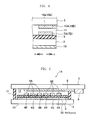
- Fig. 1 is a schematic sectional view showing the liquid crystal image display according to the first embodiment.
- Fig. 2 is a schematic plan view showing the inner surface side of a first substrate.
- Fig. 3 is a schematic plan view showing the inner surface side of a second substrate. It is to be noted that Fig. 1 is a sectional view taken along lines X-X in Figs. 2 and 3 .
- Fig. 4 is a sectional view showing a region including a transfer portion and an end of a connection wiring.
- the liquid crystal image display 1 includes a first substrate 2, a second substrate 3, a plurality of color filters 4R, 4G, 4B, a black mask 5, a plurality of common electrodes 6A, 6B (corresponding to the first electrodes as set forth in claims), transfer portions 7A, 7B, a plurality of segment electrodes 8 (corresponding to the second electrodes as set forth in claims), a monochromatic driver IC 9 (the electrode controller as set forth in claims), a plurality of connection wirings 10A, 10B, anisotropic conductive material 11, liquid crystal 12 and a backlight 13.
- the first substrate 2 and the second substrate 3 are made of a light transmitting material such as glass and bonded together at the peripheries by the anisotropic conductive material 11, as shown in Fig. 1 .
- the space surrounded by the first substrate 2, the second substrate 3 and the anisotropic conductive material 11 is filled with liquid crystal 12.
- the backlight 13 is provided on the outer surface of the first substrate 2.
- the color filters 4R, 4G, 4B, the black mask 5, the common electrodes 6A, 6B and the transfer portions 7A, 7B are provided on the first substrate 2.
- the color filters 4R, 4G and 4B selectively pass the red (R) light, the green (G) light and the blue (B) light, respectively, of the white light from the backlight 13.
- the color filters 4R, 4G and 4B are alternately arranged in the order of R, G, and B at predetermined intervals on the inner surface of the first substrate 2.
- the black mask 5 is made of a material which does not transmit light and has a thickness substantially equal to that of the color filters 4R, 4G, 4B (e.g. about 1 to 3 ⁇ m).
- the black mask is provided on the inner surface of the first substrate 2 to prevent light from traveling between the color filters 4R, 4G, 4B to reach the second substrate 3.
- the common electrodes 6A, 6B are made of a transparent conductive material such as ITO.
- the common electrodes 6A, 6B have a width substantially equal to that of the color filters 4R, 4G, 4B and formed on the color filters 4R, 4G, 4B in parallel with the color filters. In Fig. 2 , however, the color filters 4R, 4G, 4B are illustrated to be narrower than the common electrodes 6A, 6B for convenience.
- the common electrodes 6A, 6B function as scanning lines, and scanning signals are successively and periodically transmitted from the monochromatic driver IC 9 to the common electrodes.
- the ends of the common electrodes 6A, 6B in the arrows B-D direction are connected to the transfer portions 7A, 7B which are connected, via the anisotropic conductive material 11, to the connection wirings 10A, 10B, which will be described later.
- the transfer portions 7A, 7B are formed on the black mask 5 at a region outside the color filters 4R, 4G, 4B and made of the same transparent conductive material as that of the common electrodes 6A, 6B.
- the transfer portions 7A connected to the common electrodes 6A, which are the arrow A side half of the common electrodes are provided at a region on the arrow B side of the first substrate 2.
- the width of each transfer portion 7A, 7B in the arrow A-C direction is substantially twice the width of each common electrode 6A, 6B in the arrow A-C direction.
- the segment electrodes 8, the connection wirings 10A, 10B and the monochromatic driver IC 9 are provided on the second substrate 3.
- the segment electrodes 8 are made of a transparent conductive material such as ITO and formed on the inner surface of the second substrate 3 to extend perpendicularly to the common electrodes 6A, 6B. The end of each segment electrode 8 on the arrow C side is connected to the monochromatic driver IC 9.
- connection wirings 10A, 10B are made of a transparent conductive material such as ITO and extend on the second substrate 3 in parallel with the segment electrodes 8.
- the end of each of the connection wirings 10A, 10B on the arrow C side is connected to the monochromatic driver IC 9.
- the ends 10a, 10b of the connection wirings 10A, 10B in the arrow A direction are provided at locations corresponding to the transfer portions 7A, 7B on the first substrate 2.
- the ends 10a, 10b of the connection wirings 10A, 10B are connected to the transfer portions 7A, 7B via the anisotropic conductive material 11.
- the common electrodes 6A, 6B are connected to the monochromatic driver IC 9 via the transfer portions 7A, 7B and the connection wirings 10A, 10B.
- the monochromatic driver IC 9 controls signal transmission to the common electrodes 6A, 6B and the segment electrodes 8.
- the monochromatic driver IC 9 is provided on the extension of the segment electrodes 8 (in the arrow C direction) and outside the anisotropic conductive material 11.
- a color driver IC which controls each pixel as a set of three segment electrodes for R, G and B, the segment electrodes and the color filters need to be arranged in parallel with each other.
- the monochromatic driver IC 9 controls only the positions of the pixels at which light is to be transmitted. Thus, it is not necessary to arrange the segment electrodes 8 and the color filters 4R, 4G, 4B in parallel with each other. In this embodiment, the employment of the monochromatic driver IC 9 makes it possible to arrange the common electrodes 6A, 6B and the color filters 4R, 4G, 4B in parallel with each other.
- the liquid crystal image display 1 from the driver IC 9, scanning signals are periodically transmitted to the common electrodes 6A, 6B, whereas image signals for forming an image are transmitted to selected ones of the segment electrodes 8.
- voltage is applied to the liquid crystal 12 at a region where the common electrode 6A, 6B to which a scanning signal is transmitted and the segment electrode 18 to which an image signal is transmitted overlap each other.
- the light emitted from the backlight 13 and having traveled through the color filters 4R, 4G, 4B passes only through the liquid crystal 12 in the region to which the voltage is applied, whereby an intended image is formed.
- a first substrate 2 formed with color filters 4R, 4G, 4B, a black mask 5, common electrodes 6A, 6B and transfer portions 7A, 7B is prepared.
- a second substrate 3 formed with segment electrodes 8, connection wirings 10A, 10B and provided with a monochromatic driver IC 9 is prepared.
- an anisotropic conductive material 11 is applied to the first substrate 2 at a region surrounding the common electrodes 6A, 6B and including the upper surfaces of the transfer portions 7A, 7B.
- the second substrate 3 is bonded to the first substrate 2 via the anisotropic conductive material 11.
- the transfer portions 7A, 7B are connected to the connection wirings 10A, 10B via the anisotropic conductive material 11.
- the anisotropic conductive material 11 may be applied to the second substrate 3 instead of the first substrate.
- the monochromatic driver IC 9 is provided not on the first substrate 2 formed with the color filters 4R, 4G, 4B but on the second substrate 3.
- the common electrodes 6A, 6B formed on the color filters 4R, 4G, 4B are transferred to the second substrate 3 via the transfer portions 7A, 7B on the black mask 5 and connected to the monochromatic driver IC 9.
- the common electrodes 6A, 6B are connected to the monochromatic driver IC 9 without extending over a stepped portion defined between the periphery of the black mask 5 and the first substrate 2. As a result, the breakage of the common electrodes 6A, 6B due to the stepped portion does not occur, whereby the reliability of the liquid crystal image display 1 is enhanced.
- the common electrodes 6A, 6B to be transferred are formed to extend in the arrows B-D direction, i.e., perpendicularly to the arrow C direction in which the monochromatic driver IC 9 is provided.
- This arrangement makes it possible to arrange the transfer portions 7A for the half 6A of the common electrodes on the arrow B side while arranging the transfer portions 7B for the other half 6B of the common electrodes on the arrow D side.
- This arrangement of the transfer portions 7A, 7B secures a sufficient space for extending the transfer portions 7A, 7B in the arrows A-C direction.
- the length of the transfer portions 7A, 7B in the arrows A-C direction is made larger (i.e., twice) than the width of the common electrodes 6A, 6B in the in the arrows A-C direction.
- the liquid crystal image display 1 employs not a color driver IC but a monochromatic driver IC 9
- the common electrodes 6A, 6B on the color filters 4R, 4G, 4B are arranged in parallel with the color filters 4R, 4G, 4B, as shown in Figs. 1 and 2 .
- segment electrodes on the second substrate need to be arranged in parallel with the color filters on the first substrate.
- each segment electrode partially overlaps the adjacent color filter, which results in color mixing.
- such color mixing due to the positional deviation of the substrates does not occur, so that a clear image is displayed.
- FIG. 5 is a schematic sectional view showing the liquid crystal image display according to the second embodiment.
- the elements which are identical or similar to those of the first embodiment are designated by the same reference signs as those used for the first embodiment, and the description thereof will be omitted.
- the liquid crystal image display 1A includes a reflector 20 for reflecting light.
- the reflector is made of e.g. aluminum and arranged between the color filters 4R, 4G, 4B or the black mask 5 and the first substrate 2.
- the reflector 20 When the reflector 20 is provided in this way, the light having entered from the second substrate 3 side is reflected by the reflector 20 to be utilized for image forming. With this arrangement, the backlight 13 provided in the first embodiment is not necessary, so that the image display is driven by relatively low power.
- the structure of the liquid crystal image display 1A is the same as that of the liquid crystal image display 1 of the first embodiment except that the reflector 20 is provided and the backlight is eliminated.
- the liquid crystal image display of the second embodiment has the same advantages as those of the liquid crystal image display 1.
- liquid crystal image display 1 which utilizes liquid crystal 12 has been described in the foregoing embodiments, the present invention is applicable to an image display utilizing organic EL, a plasma display, an FED (field emission display) and so on.
- the number of the color filters 4R, 4G, 4B, the number of the common electrodes 6A, 6B and the number of the segment electrodes 8 may be varied appropriately.
- the common electrodes 6A, 6B are formed directly on the color filters 4R, 4G, 4B in the foregoing embodiments, the common electrodes may be formed indirectly on the color filters 4R, 4G, 4B via an additional layer provided on the color filters.
- the backlight 13 is provided on the first substrate 2 in the first embodiment, the backlight 13 may be provided on the second substrate 3. In this case, images are displayed on the first substrate 2 side.
- a backlight may be provided on the first substrate 2.
- a plurality of holes for transmitting light may be formed in a predetermined region of the reflector 20.
- transfer portions 7A, 7B are formed on the black mask 5 in the first embodiment, the transfer portions need not necessarily be formed on the black mask.
- the transfer portions may be formed on the color filters or on another member which has a thickness equal to that of the color filters and does not form a stepped portion with the color filters. To this transfer portions, the common electrodes are connected.
- a monochrome driver IC 9 is employed in the foregoing embodiments, a color driver IC may be employed instead.
Landscapes
- Physics & Mathematics (AREA)
- Nonlinear Science (AREA)
- General Physics & Mathematics (AREA)
- Mathematical Physics (AREA)
- Chemical & Material Sciences (AREA)
- Crystallography & Structural Chemistry (AREA)
- Optics & Photonics (AREA)
- Geometry (AREA)
- Liquid Crystal (AREA)
- Engineering & Computer Science (AREA)
- Theoretical Computer Science (AREA)
- Devices For Indicating Variable Information By Combining Individual Elements (AREA)
Abstract
A liquid crystal image display (1) includes a first substrate (2), a second substrate (3), anisotropic conductive material (11) for bonding the substrates (2, 3), and liquid crystal (12). The inner surface of the first substrate (2) is provided with color filters (4R, 4G, 4B), a black mask (5), common electrodes (6A, 6B) and transfer portions (7A, 7B). Segment electrodes (8), connection wirings (10A, 10B) and a monochromatic driver IC (9) are provided on the inner surface of the second substrate (3). The transfer portions (7A, 7B) at the ends of the common electrodes (6A, 6B) on the first substrate (2) are connected to the connection wirings (10A, 10B) on the second substrate (3) via the anisotropic conductive material (11). Thus, the common electrodes (6A, 6B) are connected to the monochromatic driver IC (9) without extending over the stepped portion at the periphery of the black mask (5).
Description
- The present invention relates to an image display for displaying images utilizing e.g. liquid crystal.
- Conventionally, an image display may include a pair of substrates on which electrodes are arranged perpendicularly to each other and forms images by utilizing liquid crystal sandwiched between the electrodes.
-
Patent Document 1 discloses a simple matrix image display including a pair of first and second substrates for sealing liquid crystal, color filters formed on the first substrate, first electrodes formed on the color filters to extend perpendicularly to the color filters, second electrodes formed on the second substrate to extend perpendicularly to the first electrodes, and a monochromatic driver IC provided on the extension of the first electrodes on the first substrate. - In this image display, the ends of the first electrodes on the color filters are connected to the monochromatic driver IC on the first substrate. Further, the ends of the second electrodes on the second substrate are transferred to a connection wiring formed on the first substrate and connected to the monochromatic driver IC via the connection wiring. The "transfer" here refers to the connection of an electrode formed on a substrate to a wiring or electrode formed on the other substrate.
- In this image display, color images are displayed by controlling the first electrodes and the second electrodes connected to the monochromatic driver IC. By utilizing a monochromatic driver IC which is generally inexpensive, color image display is achieved while suppressing the cost for the image display.
Patent Document 1:JP-A-2006-17919 - In this image display disclosed in
Patent Document 1, since the color filters and the monochromatic driver IC are arranged on the common substrate, the first electrodes need to extend over a stepped portion (having a height of e.g. about 1 to 3 µm) defined between the periphery of the color filter and the first substrate. Thus, the first electrodes often break at the stepped portion, so that the reliability of the display is deteriorated. The same problem occurs also when a black mask having a thickness equal to that of the color filters is provided at the periphery of the color filter. - As means for solving this problem, it may be considered to provide an additional layer between the first substrate and the monochromatic driver IC to eliminate the stepped portion. However, in view of the structure, a color filter and or the like cannot be formed under the driver IC, so that the layer needs to be made of a different material. Thus, the provision of such a layer requires an additional manufacturing step and material, which increases the manufacturing cost and the material cost. Thus, it is not practical to employ this means to solve the above-described problem.
- The present invention has been proposed to solve the above-described problems. It is, therefore, an object of the present invention to provide an image display capable of preventing breakage of the electrodes due to a stepped portion.
- To achieve the above-described object, the present invention takes the following technical measures.
- According to the invention defined in
claim 1, there is provided an image display comprising a first substrate and a second substrate facing each other and bonded together, a color filter formed on an inner surface of the first substrate, a plurality of first electrodes formed on the color filter, a plurality of second electrodes formed on an inner surface of the second substrate to extend in a direction crossing the first electrodes, and an electrode controller for controlling the first electrodes and the second electrodes. The electrode controller is provided on the inner surface of the second substrate. - According to the invention defined in
claim 2, in the image display as set forth inclaim 1, the electrode controller is provided on an extension of the second electrodes, and the first electrodes extend substantially perpendicularly to the second electrodes. - According to the invention defined in
claim 3, in the image display as set forth inclaim 1, the first electrodes are formed on the color filter and in parallel with the color filter. - According to the invention defined in claim 4, in the image display as set forth in
claim 1, the electrode controller is a monochromatic electrode controller, the first electrodes are common electrodes, and the second electrodes are segment electrodes. - According to the invention defined in
claim 5, in the image display as set forth inclaim 1, a reflector for reflecting light is provided between the color filter and the first substrate. - According to the invention defined in claim 6, in the image display as set forth in
claim 1, the image display is a liquid crystal display. -
-
Fig. 1 is a schematic sectional view showing a liquid crystal image display according to a first embodiment. -
Fig. 2 is a schematic plan view showing the inner surface side of a first substrate. -
Fig. 3 is a schematic plan view showing the inner surface side of a second substrate. -
Fig. 4 is a sectional view showing a region including a transfer portion and an end of a connection wiring. -
Fig. 5 is a schematic sectional view showing a liquid crystal image display according to a second embodiment. - A liquid crystal image display according to a first embodiment of the present invention will be described below with reference to the accompanying drawings.
-
Fig. 1 is a schematic sectional view showing the liquid crystal image display according to the first embodiment.Fig. 2 is a schematic plan view showing the inner surface side of a first substrate.Fig. 3 is a schematic plan view showing the inner surface side of a second substrate. It is to be noted thatFig. 1 is a sectional view taken along lines X-X inFigs. 2 and3 .Fig. 4 is a sectional view showing a region including a transfer portion and an end of a connection wiring. - As shown in
Figs. 1-3 , the liquidcrystal image display 1 includes afirst substrate 2, asecond substrate 3, a plurality ofcolor filters black mask 5, a plurality ofcommon electrodes transfer portions connection wirings conductive material 11,liquid crystal 12 and abacklight 13. - The
first substrate 2 and thesecond substrate 3 are made of a light transmitting material such as glass and bonded together at the peripheries by the anisotropicconductive material 11, as shown inFig. 1 . The space surrounded by thefirst substrate 2, thesecond substrate 3 and the anisotropicconductive material 11 is filled withliquid crystal 12. Thebacklight 13 is provided on the outer surface of thefirst substrate 2. - As shown in
Figs. 1 and2 , thecolor filters black mask 5, thecommon electrodes transfer portions first substrate 2. - The
color filters backlight 13. Thecolor filters first substrate 2. - The
black mask 5 is made of a material which does not transmit light and has a thickness substantially equal to that of thecolor filters first substrate 2 to prevent light from traveling between thecolor filters second substrate 3. - The
common electrodes common electrodes color filters color filters Fig. 2 , however, thecolor filters common electrodes common electrodes monochromatic driver IC 9 to the common electrodes. - The ends of the
common electrodes transfer portions conductive material 11, to theconnection wirings transfer portions black mask 5 at a region outside thecolor filters common electrodes transfer portions 7A connected to thecommon electrodes 6A, which are the arrow A side half of the common electrodes, are provided at a region on the arrow B side of thefirst substrate 2. Thetransfer portions 7B connected to thecommon electrodes 6B, which are the remaining half located on the arrow C side, are provided at a region on the arrow D side of thefirst substrate 2. The width of eachtransfer portion common electrode - As shown in
Figs. 1 and3 , thesegment electrodes 8, theconnection wirings monochromatic driver IC 9 are provided on thesecond substrate 3. - The
segment electrodes 8 are made of a transparent conductive material such as ITO and formed on the inner surface of thesecond substrate 3 to extend perpendicularly to thecommon electrodes segment electrode 8 on the arrow C side is connected to themonochromatic driver IC 9. - The
connection wirings second substrate 3 in parallel with thesegment electrodes 8. The end of each of theconnection wirings monochromatic driver IC 9. The ends 10a, 10b of theconnection wirings transfer portions first substrate 2. Thus, as shown inFig. 4 , theends connection wirings transfer portions conductive material 11. With this arrangement, thecommon electrodes monochromatic driver IC 9 via thetransfer portions connection wirings - The
monochromatic driver IC 9 controls signal transmission to thecommon electrodes segment electrodes 8. Themonochromatic driver IC 9 is provided on the extension of the segment electrodes 8 (in the arrow C direction) and outside the anisotropicconductive material 11. Herein, if a color driver IC is used which controls each pixel as a set of three segment electrodes for R, G and B, the segment electrodes and the color filters need to be arranged in parallel with each other. - Unlike this, the
monochromatic driver IC 9 controls only the positions of the pixels at which light is to be transmitted. Thus, it is not necessary to arrange thesegment electrodes 8 and thecolor filters monochromatic driver IC 9 makes it possible to arrange thecommon electrodes color filters - In the liquid
crystal image display 1, from thedriver IC 9, scanning signals are periodically transmitted to thecommon electrodes segment electrodes 8. Thus, voltage is applied to theliquid crystal 12 at a region where thecommon electrode backlight 13 and having traveled through thecolor filters liquid crystal 12 in the region to which the voltage is applied, whereby an intended image is formed. - A method for manufacturing the above-described liquid
crystal image display 1 will be described below. - First, as shown in
Fig. 2 , afirst substrate 2 formed withcolor filters black mask 5,common electrodes transfer portions Fig. 3 , asecond substrate 3 formed withsegment electrodes 8,connection wirings monochromatic driver IC 9 is prepared. Then, an anisotropicconductive material 11 is applied to thefirst substrate 2 at a region surrounding thecommon electrodes transfer portions - Then, with the
transfer portions ends connection wirings second substrate 3 is bonded to thefirst substrate 2 via the anisotropicconductive material 11. As a result, thetransfer portions connection wirings conductive material 11. Thus, the liquidcrystal image display 1 is completed. To bond thefirst substrate 2 and thesecond substrate 3 together, the anisotropicconductive material 11 may be applied to thesecond substrate 3 instead of the first substrate. - In the liquid
crystal image display 1 according to this embodiment, themonochromatic driver IC 9 is provided not on thefirst substrate 2 formed with thecolor filters second substrate 3. Thecommon electrodes color filters second substrate 3 via thetransfer portions black mask 5 and connected to themonochromatic driver IC 9. - With this arrangement, the
common electrodes monochromatic driver IC 9 without extending over a stepped portion defined between the periphery of theblack mask 5 and thefirst substrate 2. As a result, the breakage of thecommon electrodes crystal image display 1 is enhanced. - As shown in
Fig. 2 , in the liquidcrystal image display 1, thecommon electrodes monochromatic driver IC 9 is provided. This arrangement makes it possible to arrange thetransfer portions 7A for the half 6A of the common electrodes on the arrow B side while arranging thetransfer portions 7B for theother half 6B of the common electrodes on the arrow D side. This arrangement of thetransfer portions transfer portions - Unlike this embodiment, in a design in which the segment electrodes extending in the arrows A-C direction in which the
monochromatic driver IC 9 is provided are to be transferred, a space for forming the transfer portions is secured only at a region on the arrow A side, because all the segment electrodes need to be extended in the one direction (arrow C direction) in which the monochromatic driver IC is provided. In this design, therefore, it is hardly possible to form transfer portions having a dimension larger than the width of the segment electrodes. - In the liquid
crystal image display 1, however, by utilizing the sufficient space described above, the length of thetransfer portions common electrodes first substrate 2 and thesecond substrate 3 are deviated from each other in the arrows A-C direction in bonding the two substrates together, contact failure between thetransfer portions ends connection wirings - Moreover, since the liquid
crystal image display 1 employs not a color driver IC but amonochromatic driver IC 9, thecommon electrodes color filters color filters Figs. 1 and2 . Herein, when a color driver IC is employed, segment electrodes on the second substrate need to be arranged in parallel with the color filters on the first substrate. In this case, when the positions of thefirst substrate 2 and thesecond substrate 3 deviate from each other (e.g. by about 10 to 15 µm), each segment electrode partially overlaps the adjacent color filter, which results in color mixing. In the liquidcrystal image display 1, however, such color mixing due to the positional deviation of the substrates does not occur, so that a clear image is displayed. - The employment of a
monochromatic driver IC 9 reduces the cost for the parts and power consumption during the operation. - A liquid crystal image display according to a second embodiment, which is obtained by partially varying the first embodiment, will be described below with reference to
Fig. 5. Fig. 5 is a schematic sectional view showing the liquid crystal image display according to the second embodiment. In this figure, the elements which are identical or similar to those of the first embodiment are designated by the same reference signs as those used for the first embodiment, and the description thereof will be omitted. - As shown in
Fig. 5 , the liquidcrystal image display 1A according to the second embodiment includes areflector 20 for reflecting light. The reflector is made of e.g. aluminum and arranged between thecolor filters black mask 5 and thefirst substrate 2. - When the
reflector 20 is provided in this way, the light having entered from thesecond substrate 3 side is reflected by thereflector 20 to be utilized for image forming. With this arrangement, thebacklight 13 provided in the first embodiment is not necessary, so that the image display is driven by relatively low power. - The structure of the liquid
crystal image display 1A is the same as that of the liquidcrystal image display 1 of the first embodiment except that thereflector 20 is provided and the backlight is eliminated. Thus, the liquid crystal image display of the second embodiment has the same advantages as those of the liquidcrystal image display 1. - Although the present invention has been described above utilizing the embodiments, the present invention is not limited to the embodiments described in the present specification. The present invention can be varied within the spirit and scope of the invention defined by the claims. That is, the description of the present specification is merely an example and does not limit the present invention. Variations of the foregoing embodiments will be described below.
- For instance, although the liquid
crystal image display 1 which utilizesliquid crystal 12 has been described in the foregoing embodiments, the present invention is applicable to an image display utilizing organic EL, a plasma display, an FED (field emission display) and so on. - The number of the
color filters common electrodes segment electrodes 8 may be varied appropriately. - Although the
common electrodes color filters color filters - Although the
backlight 13 is provided on thefirst substrate 2 in the first embodiment, thebacklight 13 may be provided on thesecond substrate 3. In this case, images are displayed on thefirst substrate 2 side. - Although a backlight is eliminated in the second embodiment described above, a backlight may be provided on the
first substrate 2. In this case, a plurality of holes for transmitting light may be formed in a predetermined region of thereflector 20. With this arrangement, image display is possible even at a dark place. - Although
transfer portions black mask 5 in the first embodiment, the transfer portions need not necessarily be formed on the black mask. For instance, the transfer portions may be formed on the color filters or on another member which has a thickness equal to that of the color filters and does not form a stepped portion with the color filters. To this transfer portions, the common electrodes are connected. - Although a
monochrome driver IC 9 is employed in the foregoing embodiments, a color driver IC may be employed instead.
Claims (6)
- An image display comprising:a first substrate and a second substrate facing and bonded to each other;a color filter formed on an inner surface of the first substrate;a plurality of first electrodes formed on the color filter;a plurality of second electrodes formed on an inner surface of the second substrate and extending in a direction crossing the first electrodes; andan electrode controller provided on the inner surface of the second substrate for controlling the first electrodes and the second electrodes.
- The image display according to claim 1, wherein the electrode controller is provided on an extension of the second electrodes; and
wherein the first electrodes extend substantially perpendicularly to the second electrodes. - The image display according to claim 1, wherein the first electrodes are formed on the color filter and in parallel with the color filter.
- The image display according to claim 1, wherein: the electrode controller is a monochromatic electrode controller;
the first electrodes are common electrodes; and
the second electrodes are segment electrodes. - The image display according to claim 1, further comprising a light reflecting reflector provided between the color filter and the first substrate.
- The image display according to claim 1, wherein the image display is a liquid crystal display.
Applications Claiming Priority (2)
| Application Number | Priority Date | Filing Date | Title |
|---|---|---|---|
| JP2006204637A JP2008032900A (en) | 2006-07-27 | 2006-07-27 | Image display device |
| PCT/JP2007/062262 WO2008013005A1 (en) | 2006-07-27 | 2007-06-19 | Image display |
Publications (1)
| Publication Number | Publication Date |
|---|---|
| EP2053584A1 true EP2053584A1 (en) | 2009-04-29 |
Family
ID=38981320
Family Applications (1)
| Application Number | Title | Priority Date | Filing Date |
|---|---|---|---|
| EP07767152A Withdrawn EP2053584A1 (en) | 2006-07-27 | 2007-06-19 | Image display |
Country Status (6)
| Country | Link |
|---|---|
| US (1) | US20090257015A1 (en) |
| EP (1) | EP2053584A1 (en) |
| JP (1) | JP2008032900A (en) |
| KR (1) | KR20090034927A (en) |
| CN (1) | CN101496084A (en) |
| WO (1) | WO2008013005A1 (en) |
Family Cites Families (6)
| Publication number | Priority date | Publication date | Assignee | Title |
|---|---|---|---|---|
| JP3525918B2 (en) * | 2000-10-31 | 2004-05-10 | セイコーエプソン株式会社 | Electro-optical device, inspection method thereof, and electronic apparatus |
| JP3702858B2 (en) * | 2001-04-16 | 2005-10-05 | セイコーエプソン株式会社 | Electro-optical device and electronic apparatus |
| JP3909565B2 (en) * | 2001-08-10 | 2007-04-25 | セイコーエプソン株式会社 | Liquid crystal device, electronic apparatus, and method of manufacturing liquid crystal device |
| JP2003215629A (en) * | 2002-01-25 | 2003-07-30 | Kyocera Corp | Liquid crystal display device and mobile terminal or display device |
| JP3925486B2 (en) * | 2003-01-23 | 2007-06-06 | セイコーエプソン株式会社 | Electro-optical device substrate, electro-optical device, and electronic apparatus |
| JP2006017919A (en) * | 2004-06-30 | 2006-01-19 | Nanox Corp | Color liquid crystal display device |
-
2006
- 2006-07-27 JP JP2006204637A patent/JP2008032900A/en not_active Withdrawn
-
2007
- 2007-06-19 EP EP07767152A patent/EP2053584A1/en not_active Withdrawn
- 2007-06-19 US US12/375,253 patent/US20090257015A1/en not_active Abandoned
- 2007-06-19 WO PCT/JP2007/062262 patent/WO2008013005A1/en not_active Ceased
- 2007-06-19 CN CNA2007800282576A patent/CN101496084A/en active Pending
- 2007-06-19 KR KR1020097001833A patent/KR20090034927A/en not_active Ceased
Non-Patent Citations (1)
| Title |
|---|
| See references of WO2008013005A1 * |
Also Published As
| Publication number | Publication date |
|---|---|
| US20090257015A1 (en) | 2009-10-15 |
| JP2008032900A (en) | 2008-02-14 |
| WO2008013005A1 (en) | 2008-01-31 |
| CN101496084A (en) | 2009-07-29 |
| KR20090034927A (en) | 2009-04-08 |
Similar Documents
| Publication | Publication Date | Title |
|---|---|---|
| KR101313918B1 (en) | Device board | |
| US12055831B2 (en) | Display apparatus | |
| KR100778168B1 (en) | Display device | |
| CN100378510C (en) | Electro-optical devices, electronic equipment and mounting structures | |
| KR102414074B1 (en) | Curved display apparatus and method of manufacturing the same | |
| KR20030013149A (en) | a thin film transistor array for a liquid crystal display | |
| CN108700786A (en) | Active-matrix substrate and display panel | |
| KR102413480B1 (en) | Display apparatus and method of manufacturing the same | |
| KR100342242B1 (en) | Color filter for use in display apparatus | |
| JP7159429B2 (en) | Display device | |
| US11614663B2 (en) | Display device and manufacturing method thereof | |
| US20190162994A1 (en) | Electronic device | |
| US20100245747A1 (en) | Array Substrate for Liquid Crystal Panel and Liquid Crystal Panel | |
| KR101100091B1 (en) | Integrated circuit, display panel and display device for driving | |
| EP2053584A1 (en) | Image display | |
| KR100928114B1 (en) | Display device | |
| KR100568014B1 (en) | LCD panel of tiled LCD | |
| KR20190061328A (en) | Display device | |
| KR20050019994A (en) | Tcp structure of liquid crystal display | |
| US20100214520A1 (en) | Liquid Crystal Display Device | |
| JP5119941B2 (en) | Display device | |
| JPH11142867A (en) | Liquid crystal display | |
| JP3508730B2 (en) | Liquid crystal display device | |
| JP2001296561A (en) | Liquid crystal display device | |
| JP2005257899A (en) | Display device |
Legal Events
| Date | Code | Title | Description |
|---|---|---|---|
| PUAI | Public reference made under article 153(3) epc to a published international application that has entered the european phase |
Free format text: ORIGINAL CODE: 0009012 |
|
| 17P | Request for examination filed |
Effective date: 20090217 |
|
| AK | Designated contracting states |
Kind code of ref document: A1 Designated state(s): AT BE BG CH CY CZ DE DK EE ES FI FR GB GR HU IE IS IT LI LT LU LV MC MT NL PL PT RO SE SI SK TR |
|
| AX | Request for extension of the european patent |
Extension state: AL BA HR MK RS |
|
| STAA | Information on the status of an ep patent application or granted ep patent |
Free format text: STATUS: THE APPLICATION HAS BEEN WITHDRAWN |
|
| 18W | Application withdrawn |
Effective date: 20090629 |