EP2051308A2 - Method for manufacturing a nitride semiconductor device and device manufactured by the method - Google Patents
Method for manufacturing a nitride semiconductor device and device manufactured by the method Download PDFInfo
- Publication number
- EP2051308A2 EP2051308A2 EP09002185A EP09002185A EP2051308A2 EP 2051308 A2 EP2051308 A2 EP 2051308A2 EP 09002185 A EP09002185 A EP 09002185A EP 09002185 A EP09002185 A EP 09002185A EP 2051308 A2 EP2051308 A2 EP 2051308A2
- Authority
- EP
- European Patent Office
- Prior art keywords
- layer
- gan
- semiconductor device
- gallium nitride
- nitride semiconductor
- Prior art date
- Legal status (The legal status is an assumption and is not a legal conclusion. Google has not performed a legal analysis and makes no representation as to the accuracy of the status listed.)
- Granted
Links
Images


Classifications
-
- H—ELECTRICITY
- H10—SEMICONDUCTOR DEVICES; ELECTRIC SOLID-STATE DEVICES NOT OTHERWISE PROVIDED FOR
- H10P—GENERIC PROCESSES OR APPARATUS FOR THE MANUFACTURE OR TREATMENT OF DEVICES COVERED BY CLASS H10
- H10P14/00—Formation of materials, e.g. in the shape of layers or pillars
- H10P14/20—Formation of materials, e.g. in the shape of layers or pillars of semiconductor materials
- H10P14/24—Formation of materials, e.g. in the shape of layers or pillars of semiconductor materials using chemical vapour deposition [CVD]
-
- H—ELECTRICITY
- H01—ELECTRIC ELEMENTS
- H01S—DEVICES USING THE PROCESS OF LIGHT AMPLIFICATION BY STIMULATED EMISSION OF RADIATION [LASER] TO AMPLIFY OR GENERATE LIGHT; DEVICES USING STIMULATED EMISSION OF ELECTROMAGNETIC RADIATION IN WAVE RANGES OTHER THAN OPTICAL
- H01S5/00—Semiconductor lasers
- H01S5/30—Structure or shape of the active region; Materials used for the active region
- H01S5/32—Structure or shape of the active region; Materials used for the active region comprising PN junctions, e.g. hetero- or double- heterostructures
- H01S5/323—Structure or shape of the active region; Materials used for the active region comprising PN junctions, e.g. hetero- or double- heterostructures in AIIIBV compounds, e.g. AlGaAs-laser, InP-based laser
- H01S5/32308—Structure or shape of the active region; Materials used for the active region comprising PN junctions, e.g. hetero- or double- heterostructures in AIIIBV compounds, e.g. AlGaAs-laser, InP-based laser emitting light at a wavelength less than 900 nm
- H01S5/32341—Structure or shape of the active region; Materials used for the active region comprising PN junctions, e.g. hetero- or double- heterostructures in AIIIBV compounds, e.g. AlGaAs-laser, InP-based laser emitting light at a wavelength less than 900 nm blue laser based on GaN or GaP
-
- H—ELECTRICITY
- H10—SEMICONDUCTOR DEVICES; ELECTRIC SOLID-STATE DEVICES NOT OTHERWISE PROVIDED FOR
- H10H—INORGANIC LIGHT-EMITTING SEMICONDUCTOR DEVICES HAVING POTENTIAL BARRIERS
- H10H20/00—Individual inorganic light-emitting semiconductor devices having potential barriers, e.g. light-emitting diodes [LED]
- H10H20/80—Constructional details
- H10H20/81—Bodies
- H10H20/815—Bodies having stress relaxation structures, e.g. buffer layers
-
- H—ELECTRICITY
- H10—SEMICONDUCTOR DEVICES; ELECTRIC SOLID-STATE DEVICES NOT OTHERWISE PROVIDED FOR
- H10H—INORGANIC LIGHT-EMITTING SEMICONDUCTOR DEVICES HAVING POTENTIAL BARRIERS
- H10H20/00—Individual inorganic light-emitting semiconductor devices having potential barriers, e.g. light-emitting diodes [LED]
- H10H20/80—Constructional details
- H10H20/81—Bodies
- H10H20/822—Materials of the light-emitting regions
- H10H20/824—Materials of the light-emitting regions comprising only Group III-V materials, e.g. GaP
- H10H20/825—Materials of the light-emitting regions comprising only Group III-V materials, e.g. GaP containing nitrogen, e.g. GaN
-
- H—ELECTRICITY
- H10—SEMICONDUCTOR DEVICES; ELECTRIC SOLID-STATE DEVICES NOT OTHERWISE PROVIDED FOR
- H10P—GENERIC PROCESSES OR APPARATUS FOR THE MANUFACTURE OR TREATMENT OF DEVICES COVERED BY CLASS H10
- H10P14/00—Formation of materials, e.g. in the shape of layers or pillars
- H10P14/20—Formation of materials, e.g. in the shape of layers or pillars of semiconductor materials
- H10P14/29—Formation of materials, e.g. in the shape of layers or pillars of semiconductor materials characterised by the substrates
- H10P14/2901—Materials
- H10P14/2921—Materials being crystalline insulating materials
-
- H—ELECTRICITY
- H10—SEMICONDUCTOR DEVICES; ELECTRIC SOLID-STATE DEVICES NOT OTHERWISE PROVIDED FOR
- H10P—GENERIC PROCESSES OR APPARATUS FOR THE MANUFACTURE OR TREATMENT OF DEVICES COVERED BY CLASS H10
- H10P14/00—Formation of materials, e.g. in the shape of layers or pillars
- H10P14/20—Formation of materials, e.g. in the shape of layers or pillars of semiconductor materials
- H10P14/32—Formation of materials, e.g. in the shape of layers or pillars of semiconductor materials characterised by intermediate layers between substrates and deposited layers
- H10P14/3202—Materials thereof
- H10P14/3214—Materials thereof being Group IIIA-VA semiconductors
- H10P14/3216—Nitrides
-
- H—ELECTRICITY
- H10—SEMICONDUCTOR DEVICES; ELECTRIC SOLID-STATE DEVICES NOT OTHERWISE PROVIDED FOR
- H10P—GENERIC PROCESSES OR APPARATUS FOR THE MANUFACTURE OR TREATMENT OF DEVICES COVERED BY CLASS H10
- H10P14/00—Formation of materials, e.g. in the shape of layers or pillars
- H10P14/20—Formation of materials, e.g. in the shape of layers or pillars of semiconductor materials
- H10P14/32—Formation of materials, e.g. in the shape of layers or pillars of semiconductor materials characterised by intermediate layers between substrates and deposited layers
- H10P14/3242—Structure
- H10P14/3244—Layer structure
- H10P14/3248—Layer structure consisting of two layers
-
- H—ELECTRICITY
- H10—SEMICONDUCTOR DEVICES; ELECTRIC SOLID-STATE DEVICES NOT OTHERWISE PROVIDED FOR
- H10P—GENERIC PROCESSES OR APPARATUS FOR THE MANUFACTURE OR TREATMENT OF DEVICES COVERED BY CLASS H10
- H10P14/00—Formation of materials, e.g. in the shape of layers or pillars
- H10P14/20—Formation of materials, e.g. in the shape of layers or pillars of semiconductor materials
- H10P14/34—Deposited materials, e.g. layers
- H10P14/3402—Deposited materials, e.g. layers characterised by the chemical composition
- H10P14/3414—Deposited materials, e.g. layers characterised by the chemical composition being group IIIA-VIA materials
- H10P14/3416—Nitrides
-
- H—ELECTRICITY
- H10—SEMICONDUCTOR DEVICES; ELECTRIC SOLID-STATE DEVICES NOT OTHERWISE PROVIDED FOR
- H10P—GENERIC PROCESSES OR APPARATUS FOR THE MANUFACTURE OR TREATMENT OF DEVICES COVERED BY CLASS H10
- H10P14/00—Formation of materials, e.g. in the shape of layers or pillars
- H10P14/20—Formation of materials, e.g. in the shape of layers or pillars of semiconductor materials
- H10P14/34—Deposited materials, e.g. layers
- H10P14/3438—Doping during depositing
- H10P14/3441—Conductivity type
- H10P14/3444—P-type
-
- H—ELECTRICITY
- H01—ELECTRIC ELEMENTS
- H01S—DEVICES USING THE PROCESS OF LIGHT AMPLIFICATION BY STIMULATED EMISSION OF RADIATION [LASER] TO AMPLIFY OR GENERATE LIGHT; DEVICES USING STIMULATED EMISSION OF ELECTROMAGNETIC RADIATION IN WAVE RANGES OTHER THAN OPTICAL
- H01S2304/00—Special growth methods for semiconductor lasers
- H01S2304/04—MOCVD or MOVPE
-
- H—ELECTRICITY
- H10—SEMICONDUCTOR DEVICES; ELECTRIC SOLID-STATE DEVICES NOT OTHERWISE PROVIDED FOR
- H10H—INORGANIC LIGHT-EMITTING SEMICONDUCTOR DEVICES HAVING POTENTIAL BARRIERS
- H10H20/00—Individual inorganic light-emitting semiconductor devices having potential barriers, e.g. light-emitting diodes [LED]
- H10H20/01—Manufacture or treatment
- H10H20/011—Manufacture or treatment of bodies, e.g. forming semiconductor layers
- H10H20/013—Manufacture or treatment of bodies, e.g. forming semiconductor layers having light-emitting regions comprising only Group III-V materials
- H10H20/0133—Manufacture or treatment of bodies, e.g. forming semiconductor layers having light-emitting regions comprising only Group III-V materials with a substrate not being Group III-V materials
- H10H20/01335—Manufacture or treatment of bodies, e.g. forming semiconductor layers having light-emitting regions comprising only Group III-V materials with a substrate not being Group III-V materials the light-emitting regions comprising nitride materials
Definitions
- the present invention relates to a method for manufacturing a group III nitride semiconductor device.
- a semiconductor laser device is manufactured by forming a semiconductor single-crystal film on a crystal substrate. Characteristics of a light emitting device as a laser device are greatly dependent on the density of crystal defects in the single-crystal film. From this point of view, the substrate is preferable to be made of a material having the physical-property constants such as crystal structure, lattice constant, and thermal-expansion coefficient the same as those of a semiconductor crystal to be expitaxially grown on the substrate.
- GaN gallium nitride
- GaN gallium nitride
- a GaN single-crystal ingot having a size usable as a wafer has never been formed. Therefore, a sapphire substrate has been used as a substrate.
- MOCVD Metal-organic chemical vapor deposition
- TMG trimethylgallium
- NH 3 ammonia
- the crystal is grown at the temperatures of 900-1100°C.
- semiconductor crystal such as gallium arsenide (GaAs) is unstable so that it is not a proper material for a substrate.
- GaAs gallium arsenide
- single-crystal sapphire is adopted as a substrate. This is because sapphire is stable at the above high temperature though the physical properties of sapphire are different from those of GaN.
- the direct growth of GaN on a sapphire substrate can not produce a higher-quality single-crystal film for a light emitting element, because sapphire has a lattice constant different from that of GaN by approximately 14%. Therefore, an approach, known as the two-step-growth method, to moderate the misfit of the lattice constant between a GaN single-crystal film and sapphire, has been developed.
- the steps in the two-step-growth method are: forming a low temperature buffer layer of aluminum nitride (AlN) or GaN on a sapphire substrate at a low temperature of 400-600°C, heating the substrate with the buffer layer, and then epitaxial-growing GaN on the buffer layer.
- AlN aluminum nitride
- the two-step-growth method has stably produced a comparatively smooth single-crystal film.
- the GaN film produced by the above method has high-density defects of 1 ⁇ 10 8 -1 ⁇ 10 10 (1/cm 2 ), and the above value shows a very high density, which is 10,000-100,000 times greater than that of GaAs.
- Such a defect is called "threading dislocation", which is linearly extending crystal defect that penetrates a crystal film from its top to the bottom.
- the threading dislocation works as the non-radiative recombination center of carriers. Therefore, it is known that as the threading dislocation density increases, the light emitting efficiency of the semiconductor crystal decreases.
- the dislocation density depends on conditions of the epitaxial growth, and particularly depends on the growth pressure. Moreover, it is known that the threading dislocation density decreases as the growth pressure increases, as described in Japan Journal of Applied Physics, Vol. 37 (1998) p. 4460-4466 . Therefore, the epitaxial growth on a sapphire substrate is generally performed at approximately atmosphere pressure (760torr).
- the pit density also greatly depends on the growth pressure and that it increases more as the growth pressure increases. Therefore, as described above, it is clear that a dislocation density and a pit density are mutually contradictory. Thus, a problem arises that the increase of the growth pressure for decreasing a dislocation density may cause the increase of a pit density, thereby leading to the decrease of a manufacturing yield of a device.
- An object of the present invention is to solve the above problems to provide a nitride semiconductor device and a method for manufacturing the nitride semiconductor device which has a reduced dislocation density while suppressing the generation of pits in a GaN layer.
- a method for manufacturing a nitride semiconductor device is characterized in that the method comprises the steps of successively depositing a group III nitride semiconductor (In x Ga (1-x-y) Al y N (0 ⁇ x ⁇ 1, 0 ⁇ y ⁇ 1)) on a flat sapphire substrate by metal-organic chemical vapor deposition.
- a group III nitride semiconductor In x Ga (1-x-y) Al y N (0 ⁇ x ⁇ 1, 0 ⁇ y ⁇ 1)
- the method comprises the steps of: forming a low temperature buffer layer on the sapphire substrate, forming a first gallium nitride layer on the low temperature buffer layer by supplying a first mixed gas containing no dopant component, and forming a second gallium nitride layer containing a dopant on the first gallium nitride layer while filling voids and flattening a surface of the first gallium nitride layer by supplying a second mixed gas containing a dopant component.
- a nitride semiconductor device is characterized in that the device is manufactured by depositing a group III nitride semiconductor (In x Ga ( 1-x-y) Al y N (0 ⁇ x ⁇ 1, 0 ⁇ y ⁇ 1)) on a flat sapphire substrate.
- a group III nitride semiconductor In x Ga ( 1-x-y) Al y N (0 ⁇ x ⁇ 1, 0 ⁇ y ⁇ 1)
- the group III nitride semiconductor device comprises a low temperature buffer layer deposited on the sapphire substrate; a first gallium nitride layer having a first predetermined thickness, containing no dopant component, and being deposited on the low temperature buffer layer; and a second gallium nitride layer having a second predetermined thickness containing a dopant component, the second gallium nitride layer being deposited on the first gallium nitride layer; wherein the second gallium nitride layer is deposited while flattening the surface of the first gallium nitride layer by filling voids in the first gallium nitride layer.
- a nitride semiconductor device comprises a multilayer structure in which nitride semiconductor single-crystal layers are formed on a sapphire substrate 1.
- a low temperature buffer layer 2 of AlN or GaN is formed on the sapphire substrate 1.
- a non-doped GaN crystal layer 3 is formed on the low-temperature buffer layer 2 as a first GaN layer.
- the non-doped GaN crystal layer 3 takes on an island-like structure without any dopant.
- a second GaN layer 4 containing a dopant is formed on the first GaN layer.
- the second GaN layer 4 is deposited while filling pyramidal surface voids in the first GaN layer 3 and flattening the surface of the GaN layer 3.
- a non-doped GaN crystal film 5 is formed on the second GaN layer 4 as a third GaN layer. Further, a crystal layer 6 is formed on the layer 5. In this embodiment, it should be noted that the crystal layer 6 is made of Sidoped n-type GaN.
- an n-type cladding layer 7, an active layer 8, a p-type cladding 9, and a p-type contact layer 10 are formed in the stated order on the layer 6.
- a p-type electrode 11 and an n-type electrode 12 are formed on the p-type contact layer 10 and the fourth crystal layer 6, respectively.
- FIGS. 2 and 3 A method for manufacturing a nitride semiconductor device according to the present invention will be described below in conjunction with FIGS. 2 and 3 .
- a sapphire substrate 1 is loaded into a layer-forming MOCVD reactor. Then, the substrate 1 is placed in a hydrogen gas flow having a pressure of 300torr at a temperature of 1050°C for 10 minutes to heat-clean the surface of the sapphire substrate 1. Thereafter, the sapphire substrate 1 is cooled to the temperature of 400°C. Then, anmonia NH 3 as nitrogen precursor material and trimethyl aluminuman TMA as a Al precursor material are introduced into the reactor to deposit AlN, thereby forming a low-temperature buffer layer 2 of AlN having a thickness of 50nm (step S1).
- the growth pressure is changed from 300torr to 600torr while only NH 3 gas is flowing through the reactor.
- the sapphire substrate 1 with the low-temperature buffer layer 2 is heated up to the temperature of 1050°C again.
- TMG trimethylgallium
- step S2 GaN-crystal nuclei are initially produced on the low-temperature buffer layer 2. The nuclei proceed to three-dimensional growth, and continuously grow while forming an island-like structure.
- the non-doped GaN layer 3 is grown to a nominal thickness of approximately 0.5 ⁇ m, the supply of TMG is stopped and the pressure is changed to 300torr again. It should be understood that the nominal thickness value assumes that a layer grows uniformly.
- Et-Cp2Mg ethyl-biscyclopentadienylmagnesium
- TMG and NH 3 a second mixed gas
- Mg Mg
- the deposition of a GaN:Mg layer 4 as a second GaN layer is then started (step S3).
- a flow rate of Et-Cp2Mg is selected so that an atomic concentration of Mg is selected to be 1 ⁇ 10 18 -5 ⁇ 10 20 (1/cc).
- a concentration of Mg is selected so that it promotes the two-dimensional growth of the GaN:Mg layer.
- the GaN:Mg layer 4 is grown to a nominal thickness of 0.5 ⁇ m.
- the GaN:Mg layer 4 has a thickness of 0.5 ⁇ m.
- the GaN:Mg layer 4 may have any thickness, as long as pits formed on the surface of the non-doped GaN layer 3 are filled to flatten the surface of the GaN:Mg layer 4.
- step S4 the only supply of Et-Cp2Mg is stopped to cause a non-doped GaN layer 5 to be grown for 1-10 minutes (step S4).
- Me-SiH 3 methylsilane
- step S5 the flow rate of Me-SiH 3 is set so that an atomic concentration of Si is set to be 1 ⁇ 10 17 (1/cc).
- the supply of TMG and Me-SiH 3 is stopped, and the substrate starts to be cooled.
- the supply of NH 3 is also stopped.
- the substrate temperature is cooled to room temperature, the substrate is unloaded out of the reactor. This is used as a sample (1) for a comparison to be described later.
- an n-type cladding layer 7, an active layer 8, a p-type cladding layer 9, and a p-type contact layer 10 are deposited in order on the GaN:Si layer 6.
- a p-type electrode 11 and an n-type electrode 12 are then formed on the p-type contact layer 10 and the fourth crystal layer 6, respectively (step S6). As described above, a semiconductor device is manufactured.
- a sample (2) is manufactured by growing the first GaN layer 3 and then growing the GaN:Si layer 6 to 2 ⁇ m while keeping the pressure at 600torr.
- a sample (3) is manufactured by growing both of the first GaN layer 3 and GaN:Si layer 6 at a pressure of 300torr.
- the first GaN layer 3 preferably has a thickness at which the growth of a non-doped GaN layer starts to change from an initial three-dimensional growth form to a two-dimensional growth form.
- the thickness mentioned above is suitable for two-dimensional growth of the second GaN layer. Therefore, the first GaN film 3 has a thickness of 0.2 ⁇ m as its lower limit, at which crystal nuclei start to combine.
- the first GaN film 3 increases, the depth of a pit formed on the surface may increase. This leads the GaN:Mg layer 4 over the pits to have an increasing thickness in order to fill the pits. Therefore, the first GaN film 3 also has a thickness of 4 ⁇ m as its upper limit in view of shortening the time required to fill voids in the island-like structure for flattening the layer.
- the non-doped GaN layer 5 is formed between the GaN:Mg layer 4 and the GaN:Si layer 6 in order to prevent Mg from affecting the growth of the GaN:Si layer 6.
- Mg may remain in the reactor and/or pipe for a while after stopping the supply of Et-Cp2Mg (this phenomenon is called Mg memory effect). Therefore, if the GaN:Si layer 6 is grown just after forming the GaN:Mg layer 4, Mg remaining in the reactor or the pipe may be deposited on the surface in the period from the stop of the supply of Et-Cp2Mg to the start of the growth of the GaN:Si layer 6.
- the remaining Mg causes the GaN:Si layer 6 to start the three-dimensional growth again, when the GaN:Si layer 6 starts to grow. This may adversely increase the number of pits.
- the Mg memory effect does not always occur. The memory effect depends on a design of an MOCVD reactor or a depositing condition of the GaN:Si layer 6, so that it may not occur immediately after stopping the supply of Et-Cp2Mg. Therefore, it should be noted that the deposition of the non-doped GaN layer 5 may be omitted.
- an Si atomic concentration of the GaN:Si layer 6 is not restricted to 1 ⁇ 10 17 (1/cc) of this embodiment. It is also within the scope of the invention to provide the general concentration of a N + layer (Si concentration; 1 ⁇ 10 18 -1 ⁇ 10 19 (1/cm 3 )) as the group III nitride semiconductor device formed on a sapphire substrate.
- GaN-based crystal takes three-dimensional growth, because a crystal plane (1-101) and its near high-order planes are dominant in the initial growth stage. When three-dimensionally growing islands start to collide and combine, high-order planes are changing to the plane (1-101) and another stable plane (0001). It is known that the growth rate of the plane (0001) is slow. This probably results from the fact that Ga atoms having reached the plane (0001) migrate over the plane (0001), and are then captured into the plane (1-101). Thus, the plane (1-101) grows more quickly and the plane (0001) remains, so that a film is being slowly flattened.
- Mg is considered as an acceptor-like impurity to be replacable with Ga at a Ga atomic position. It is within the invention to replace Mg with another atomic element as one of the group II elements Be, Ca, and Zn which serve as acceptor-like impurities at the Ga atomic position. Then, it is also within the invention to grow a GaN layer including the replaced element as a dopant.
- the second GaN layer can grow while filling voids in the first GaN layer in its growth process, by depositing the non-doped first GaN layer on the low-temperature buffer layer to suppress the generation of threading dislocations, and then depositing a second GaN film with a dopant. Therefore, the number of pits generated in the GaN layer can be reduced. As a result, the surface of the GaN layer can be flattened, while threading dislocations generated inside the GaN layer can be reduced. Thus, the present invention can improve characteristics of the group III nitride semiconductor device comprising the GaN film.
Landscapes
- Physics & Mathematics (AREA)
- Condensed Matter Physics & Semiconductors (AREA)
- General Physics & Mathematics (AREA)
- Electromagnetism (AREA)
- Optics & Photonics (AREA)
- Led Devices (AREA)
- Semiconductor Lasers (AREA)
Abstract
Description
- The present invention relates to a method for manufacturing a group III nitride semiconductor device.
- Extensive researches is now underway on nitride-gallium and related compound semiconductor as a material system for short wavelength light emitting devices, in particular short wave length semiconductors lasers. A semiconductor laser device is manufactured by forming a semiconductor single-crystal film on a crystal substrate. Characteristics of a light emitting device as a laser device are greatly dependent on the density of crystal defects in the single-crystal film. From this point of view, the substrate is preferable to be made of a material having the physical-property constants such as crystal structure, lattice constant, and thermal-expansion coefficient the same as those of a semiconductor crystal to be expitaxially grown on the substrate. For example, it is ideal to use a single crystal of gallium nitride (hereinafter referred to as GaN), which is the same as an epitaxial film. However, it is very difficult to form a large crystal of GaN. A GaN single-crystal ingot having a size usable as a wafer has never been formed. Therefore, a sapphire substrate has been used as a substrate.
- Metal-organic chemical vapor deposition (hereinafter referred to as MOCVD) is most generally used to form a GaN single-crystal film. In this method, trimethylgallium (referred to as TMG hereinafter) is used as a group III precursor material, and ammonia (referred to as NH3 hereinafter) is used as a group V precursor material for the material of the MOCVD.
- When forming a GaN semiconductor film by the above method, the crystal is grown at the temperatures of 900-1100°C. At the higher temperature, semiconductor crystal such as gallium arsenide (GaAs) is unstable so that it is not a proper material for a substrate. Thus, single-crystal sapphire is adopted as a substrate. This is because sapphire is stable at the above high temperature though the physical properties of sapphire are different from those of GaN.
- However, the direct growth of GaN on a sapphire substrate can not produce a higher-quality single-crystal film for a light emitting element, because sapphire has a lattice constant different from that of GaN by approximately 14%. Therefore, an approach, known as the two-step-growth method, to moderate the misfit of the lattice constant between a GaN single-crystal film and sapphire, has been developed. The steps in the two-step-growth method are: forming a low temperature buffer layer of aluminum nitride (AlN) or GaN on a sapphire substrate at a low temperature of 400-600°C, heating the substrate with the buffer layer, and then epitaxial-growing GaN on the buffer layer. Thus, the two-step-growth method has stably produced a comparatively smooth single-crystal film.
- However, it has been found that the GaN film produced by the above method has high-density defects of 1×10⁸-1×10¹⁰ (1/cm2), and the above value shows a very high density, which is 10,000-100,000 times greater than that of GaAs. Such a defect is called "threading dislocation", which is linearly extending crystal defect that penetrates a crystal film from its top to the bottom. The threading dislocation works as the non-radiative recombination center of carriers. Therefore, it is known that as the threading dislocation density increases, the light emitting efficiency of the semiconductor crystal decreases.
- Though a light emitting efficiency characteristic of GaN is less affected by the dislocation density, compared to that of a conventional optical semiconductor such as GaAs, the existence of a large number of dislocation degrades the light emitting efficiency.
- The dislocation density depends on conditions of the epitaxial growth, and particularly depends on the growth pressure. Moreover, it is known that the threading dislocation density decreases as the growth pressure increases, as described in Japan Journal of Applied Physics, Vol. 37 (1998) p. 4460-4466. Therefore, the epitaxial growth on a sapphire substrate is generally performed at approximately atmosphere pressure (760torr).
- It is known that crystal nuclei grow three-dimensionally, like islands, at the beginning of growth, and that they then combine and grow two-dimensionally, when a low-temperature buffer layer of GaN or AlN is formed on a sapphire substrate and then the GaN crystal is grown on the buffer layer at a higher temperature (approximately 1000°C). Therefore, a hexagonal-pyramidal hole called a "pit" may be formed in the GaN expitaxial film. The presence of pits makes the production of a good device on or near the pit difficult. That is, a higher pit density of an expitaxial wafer may result in the decrease of device production during manufacturing.
- It is known that the pit density also greatly depends on the growth pressure and that it increases more as the growth pressure increases. Therefore, as described above, it is clear that a dislocation density and a pit density are mutually contradictory. Thus, a problem arises that the increase of the growth pressure for decreasing a dislocation density may cause the increase of a pit density, thereby leading to the decrease of a manufacturing yield of a device.
- An object of the present invention is to solve the above problems to provide a nitride semiconductor device and a method for manufacturing the nitride semiconductor device which has a reduced dislocation density while suppressing the generation of pits in a GaN layer.
- A method for manufacturing a nitride semiconductor device according to the present invention is characterized in that the method comprises the steps of successively depositing a group III nitride semiconductor (InxGa(1-x-y)AlyN (0≤x≤1, 0≤y≤1)) on a flat sapphire substrate by metal-organic chemical vapor deposition. The method comprises the steps of: forming a low temperature buffer layer on the sapphire substrate, forming a first gallium nitride layer on the low temperature buffer layer by supplying a first mixed gas containing no dopant component, and forming a second gallium nitride layer containing a dopant on the first gallium nitride layer while filling voids and flattening a surface of the first gallium nitride layer by supplying a second mixed gas containing a dopant component.
- A nitride semiconductor device according to the present invention is characterized in that the device is manufactured by depositing a group III nitride semiconductor (InxGa( 1-x-y)AlyN (0≤x≤1, 0≤y≤1)) on a flat sapphire substrate. The group III nitride semiconductor device comprises a low temperature buffer layer deposited on the sapphire substrate; a first gallium nitride layer having a first predetermined thickness, containing no dopant component, and being deposited on the low temperature buffer layer; and a second gallium nitride layer having a second predetermined thickness containing a dopant component, the second gallium nitride layer being deposited on the first gallium nitride layer; wherein the second gallium nitride layer is deposited while flattening the surface of the first gallium nitride layer by filling voids in the first gallium nitride layer.
- The aforementioned aspects and other features of the invention are explained in the following description, taken in connection with the accompanying drawing figures wherein:
-
FIG. 1 is a sectional view showing a nitride semiconductor device according to the present invention; -
FIG. 2 is a partial enlarged sectional view of the nitride semiconductor device shown inFIG. 1 ; and -
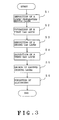
FIG. 3 is a flow chart showing a method for manufacturing a nitride semiconductor device according to the present invention. - The present invention will be described in conjunction with a preferred embodiment, referring to the accompanying drawings.
- As shown in
FIG. 1 , a nitride semiconductor device according to the present invention comprises a multilayer structure in which nitride semiconductor single-crystal layers are formed on asapphire substrate 1. A lowtemperature buffer layer 2 of AlN or GaN is formed on thesapphire substrate 1. A non-dopedGaN crystal layer 3 is formed on the low-temperature buffer layer 2 as a first GaN layer. The non-dopedGaN crystal layer 3 takes on an island-like structure without any dopant. Asecond GaN layer 4 containing a dopant is formed on the first GaN layer. Thesecond GaN layer 4 is deposited while filling pyramidal surface voids in thefirst GaN layer 3 and flattening the surface of theGaN layer 3. - Moreover, a non-doped GaN
crystal film 5 is formed on thesecond GaN layer 4 as a third GaN layer. Further, acrystal layer 6 is formed on thelayer 5. In this embodiment, it should be noted that thecrystal layer 6 is made of Sidoped n-type GaN. - Furthermore, an n-
type cladding layer 7, an active layer 8, a p-type cladding 9, and a p-type contact layer 10 are formed in the stated order on thelayer 6. Then, a p-type electrode 11 and an n-type electrode 12 are formed on the p-type contact layer 10 and thefourth crystal layer 6, respectively. Thus, a semiconductor light emitting device is manufactured. - A method for manufacturing a nitride semiconductor device according to the present invention will be described below in conjunction with
FIGS. 2 and3 . - A
sapphire substrate 1 is loaded into a layer-forming MOCVD reactor. Then, thesubstrate 1 is placed in a hydrogen gas flow having a pressure of 300torr at a temperature of 1050°C for 10 minutes to heat-clean the surface of thesapphire substrate 1. Thereafter, thesapphire substrate 1 is cooled to the temperature of 400°C. Then, anmonia NH3 as nitrogen precursor material and trimethyl aluminuman TMA as a Al precursor material are introduced into the reactor to deposit AlN, thereby forming a low-temperature buffer layer 2 of AlN having a thickness of 50nm (step S1). - Then, after stopping the supply of TMA, the growth pressure is changed from 300torr to 600torr while only NH3 gas is flowing through the reactor. Moreover, the
sapphire substrate 1 with the low-temperature buffer layer 2 is heated up to the temperature of 1050°C again. TMG (trimethylgallium) is then introduced as a first mixed gas to cause anon-doped GaN layer 3 to be grown (step S2). While thenon-doped GaN layer 3 is deposited, GaN-crystal nuclei are initially produced on the low-temperature buffer layer 2. The nuclei proceed to three-dimensional growth, and continuously grow while forming an island-like structure. - When the
non-doped GaN layer 3 is grown to a nominal thickness of approximately 0.5µm, the supply of TMG is stopped and the pressure is changed to 300torr again. It should be understood that the nominal thickness value assumes that a layer grows uniformly. - Then, Et-Cp2Mg (ethyl-biscyclopentadienylmagnesium) is introduced into the reactor in conjunction with TMG and NH3 as a second mixed gas in order to use Mg as a dopant. The deposition of a GaN:
Mg layer 4 as a second GaN layer is then started (step S3). In this embodiment, a flow rate of Et-Cp2Mg is selected so that an atomic concentration of Mg is selected to be 1×10¹⁸-5×10²⁰(1/cc). A concentration of Mg is selected so that it promotes the two-dimensional growth of the GaN:Mg layer. The GaN:Mg layer 4 is grown to a nominal thickness of 0.5µm. - In this embodiment, the GaN:
Mg layer 4 has a thickness of 0.5µm. However, it should be noted that the GaN:Mg layer 4 may have any thickness, as long as pits formed on the surface of thenon-doped GaN layer 3 are filled to flatten the surface of the GaN:Mg layer 4. - Then, the only supply of Et-Cp2Mg is stopped to cause a
non-doped GaN layer 5 to be grown for 1-10 minutes (step S4). Then, Me-SiH3 (methylsilane) is introduced to grow a GaN:Si layer 6 of 2µm (step S5). In this embodiment, the flow rate of Me-SiH3 is set so that an atomic concentration of Si is set to be 1×10¹⁷(1/cc). - When growth of the GaN:
Si layer 6 is completed, the supply of TMG and Me-SiH3 is stopped, and the substrate starts to be cooled. When a substrate is cooled to a temperature of 400°C or lower, the supply of NH3 is also stopped. Moreover, when the substrate temperature is cooled to room temperature, the substrate is unloaded out of the reactor. This is used as a sample (1) for a comparison to be described later. - Furthermore, an n-
type cladding layer 7, an active layer 8, a p-type cladding layer 9, and a p-type contact layer 10 are deposited in order on the GaN:Si layer 6. A p-type electrode 11 and an n-type electrode 12 are then formed on the p-type contact layer 10 and thefourth crystal layer 6, respectively (step S6). As described above, a semiconductor device is manufactured. - For comparison with the sample (1), a sample (2) is manufactured by growing the
first GaN layer 3 and then growing the GaN:Si layer 6 to 2 µm while keeping the pressure at 600torr. Moreover, a sample (3) is manufactured by growing both of thefirst GaN layer 3 and GaN:Si layer 6 at a pressure of 300torr. When comparing the samples (2) and (3) with the sample (1), conditions such as film thicknesses and doping concentrations are the same except that the samples (2) and (3) lack of thesecond GaN layer 4 andnon-doped GaN layer 5. - The pit density of the surface, Hall mobility, and EPD or dislocation density of each of the sample were evaluated. The results are shown in Table 1.
[Table 1] Pit density
(1/mm2)Hall mobility
(cm2/Vs)EPD (1/cm2) Sample (1) 73 437 1.2 × 10⁹ Sample (2) 650 451 1.2 × 10⁹ Sample (3) 20 107 8.6 × 10⁹ - Referring to Table 1, it can be seen that Hall mobility correlates with EPD and that the EPD decreases as the Hall mobility increases. Moreover, it is found that EPDs of the samples (1) and (2) are lower than the EPD of the sample (3). The samples (1) and (3) respectively have a low pit density but the sample (2) has a high pit density. Furthermore, it is found that all pits on the
first GaN layer 3 are filled with thesecond GaN layer 4, and that the film has a flattened upper surface over the pits. The finding was made by observing a cross section of the sample (1) with a scanning electron microscope (SEM). Thus, a propagation of pits in the thickness direction, which generated in the first GaN layer, can be avoided while suppressing the increase of the dislocation density. - Moreover, the
first GaN layer 3 preferably has a thickness at which the growth of a non-doped GaN layer starts to change from an initial three-dimensional growth form to a two-dimensional growth form. The thickness mentioned above is suitable for two-dimensional growth of the second GaN layer. Therefore, thefirst GaN film 3 has a thickness of 0.2µm as its lower limit, at which crystal nuclei start to combine. As the thickness of thefirst GaN layer 3 increases, the depth of a pit formed on the surface may increase. This leads the GaN:Mg layer 4 over the pits to have an increasing thickness in order to fill the pits. Therefore, thefirst GaN film 3 also has a thickness of 4µm as its upper limit in view of shortening the time required to fill voids in the island-like structure for flattening the layer. - The
non-doped GaN layer 5 is formed between the GaN:Mg layer 4 and the GaN:Si layer 6 in order to prevent Mg from affecting the growth of the GaN:Si layer 6. The reason is described below. That is, Mg may remain in the reactor and/or pipe for a while after stopping the supply of Et-Cp2Mg (this phenomenon is called Mg memory effect). Therefore, if the GaN:Si layer 6 is grown just after forming the GaN:Mg layer 4, Mg remaining in the reactor or the pipe may be deposited on the surface in the period from the stop of the supply of Et-Cp2Mg to the start of the growth of the GaN:Si layer 6. Therefore, the remaining Mg causes the GaN:Si layer 6 to start the three-dimensional growth again, when the GaN:Si layer 6 starts to grow. This may adversely increase the number of pits. However, the Mg memory effect does not always occur. The memory effect depends on a design of an MOCVD reactor or a depositing condition of the GaN:Si layer 6, so that it may not occur immediately after stopping the supply of Et-Cp2Mg. Therefore, it should be noted that the deposition of thenon-doped GaN layer 5 may be omitted. - Moreover, it should be understood that an Si atomic concentration of the GaN:
Si layer 6 is not restricted to 1×10¹⁷(1/cc) of this embodiment. It is also within the scope of the invention to provide the general concentration of a N+ layer (Si concentration; 1×10¹⁸-1×10¹⁹(1/cm3)) as the group III nitride semiconductor device formed on a sapphire substrate. - In general, GaN-based crystal takes three-dimensional growth, because a crystal plane (1-101) and its near high-order planes are dominant in the initial growth stage. When three-dimensionally growing islands start to collide and combine, high-order planes are changing to the plane (1-101) and another stable plane (0001). It is known that the growth rate of the plane (0001) is slow. This probably results from the fact that Ga atoms having reached the plane (0001) migrate over the plane (0001), and are then captured into the plane (1-101). Thus, the plane (1-101) grows more quickly and the plane (0001) remains, so that a film is being slowly flattened.
- When a precursor material diffuses quickly, nuclei grow uniformly, and uniform islands are simultaneously generating at a high density during the growth in low pressure, the above mechanism for changing into two-dimensional growth works quickly to flatten the surface of the layer. However, crystal defects such as threading dislocations are generated, when growing planes produced from another initial nuclei collide with each other. Therefore, a dislocation density tends to become higher in a growing mode in which an island density is higher and a combination rate is fast.
- When a growth pressure is higher, competition occurs among initial nuclei due to selective growth and large islands are produced at a comparatively low density. Therefore, dislocation density decreases. However, a large and deep pit consisting of the plane (1-101) is easily produced, because islands combine slowly. Therefore, the pit does not disappear, because supply of a precursor material diffusion to the pit is reduced, and tends to become larger as film growth progresses.
- However, when the three-dimensional growth is changing to two-dimensional growth, the presence of Mg results in the promotion of migration of Ga atoms on the plane (0001). Therefore, a growth-rate ratio between the plane (1-101) and its near plane further increases, so that the transition from the three-dimensional growth to the two-dimensional growth is promoted.
- Thus, Mg is considered as an acceptor-like impurity to be replacable with Ga at a Ga atomic position. It is within the invention to replace Mg with another atomic element as one of the group II elements Be, Ca, and Zn which serve as acceptor-like impurities at the Ga atomic position. Then, it is also within the invention to grow a GaN layer including the replaced element as a dopant.
- Moreover, it is found through experiments that it is effective to flatten the surface of the first GaN layer when the pressure of the second GaN layer growth is decreased to a level below that of a first GaN layer growth.
- Thus, the second GaN layer can grow while filling voids in the first GaN layer in its growth process, by depositing the non-doped first GaN layer on the low-temperature buffer layer to suppress the generation of threading dislocations, and then depositing a second GaN film with a dopant. Therefore, the number of pits generated in the GaN layer can be reduced. As a result, the surface of the GaN layer can be flattened, while threading dislocations generated inside the GaN layer can be reduced. Thus, the present invention can improve characteristics of the group III nitride semiconductor device comprising the GaN film.
- It is understood that the foregoing description and accompanying drawings set forth the preferred embodiments of the invention at the present time. Various modifications, additions and alternative designs will, of course, become apparent to those skilled in the art in light of the foregoing teachings without departing from the spirit and scope of the disclosed invention. Thus, it should be appreciated that the invention is not limited to the disclosed embodiments but may be practiced within the full scope of the appended claims.
Claims (7)
- A nitride semiconductor device successively formed from group III nitride semiconductor layers of InxGa(1-x-y)AlyN where 0≦x≦1, 0≦y≦1 over a flat surface of a sapphire substrate (1), said device comprising:a buffer layer (2) formed on said sapphire substrate (1) ;a first gallium nitride layer (3) containing no dopant component, formed on said buffer layer (2);a second gallium nitride layer (4) containing a dopant component, formed on said first gallium nitride layer (3); anda third gallium nitride layer (5) containing no dopant component, formed on said second gallium nitride layer (4), whereinthe first gallium nitride layer (3) has pits on the second gallium nitride layer side interface; wherein the pits of said first gallium nitride layer (3) are filled with the second gallium nitride layer (4); wherein the second gallium nitride layer (4) has a flat surface; and wherein the dopant of the second gallium nitride layer (4) is at least one of Mg, Be, Ca and Zn.
- The nitride semiconductor device according to claim 1, further comprising a fourth gallium nitride layer (6) containing Si, formed on and in contact with said third gallium nitride layer (5).
- The nitride semiconductor device according to claim 1, the buffer layer (2) is made of AlN or GaN.
- The nitride semiconductor device according to claim 1, wherein the pits of said first gallium nitride layer (3) are hexagonal-pyramidal holes.
- The nitride semiconductor device according to claim 4, wherein the hexagonal-pyramidal holes include facet plane (1-101).
- The nitride semiconductor device according to claim 1, wherein said second gallium nitride film (4) has a thickness sufficient to flatten the surface thereof.
- The nitride semiconductor device according to claim 1, wherein said first gallium nitride layer (3) has a thickness of 0.2 - 4µm.
Applications Claiming Priority (2)
| Application Number | Priority Date | Filing Date | Title |
|---|---|---|---|
| JP16416999A JP3786544B2 (en) | 1999-06-10 | 1999-06-10 | Nitride semiconductor device manufacturing method and device manufactured by the method |
| EP00111833A EP1059677B1 (en) | 1999-06-10 | 2000-06-07 | Method for manufacturing a nitride semiconductor device |
Related Parent Applications (2)
| Application Number | Title | Priority Date | Filing Date |
|---|---|---|---|
| EP00111833A Division EP1059677B1 (en) | 1999-06-10 | 2000-06-07 | Method for manufacturing a nitride semiconductor device |
| EP00111833.0 Division | 2000-06-07 |
Publications (3)
| Publication Number | Publication Date |
|---|---|
| EP2051308A2 true EP2051308A2 (en) | 2009-04-22 |
| EP2051308A3 EP2051308A3 (en) | 2010-04-14 |
| EP2051308B1 EP2051308B1 (en) | 2012-02-22 |
Family
ID=15788050
Family Applications (2)
| Application Number | Title | Priority Date | Filing Date |
|---|---|---|---|
| EP09002185A Expired - Lifetime EP2051308B1 (en) | 1999-06-10 | 2000-06-07 | Group III nitride semiconductor device |
| EP00111833A Expired - Lifetime EP1059677B1 (en) | 1999-06-10 | 2000-06-07 | Method for manufacturing a nitride semiconductor device |
Family Applications After (1)
| Application Number | Title | Priority Date | Filing Date |
|---|---|---|---|
| EP00111833A Expired - Lifetime EP1059677B1 (en) | 1999-06-10 | 2000-06-07 | Method for manufacturing a nitride semiconductor device |
Country Status (3)
| Country | Link |
|---|---|
| US (1) | US6555846B1 (en) |
| EP (2) | EP2051308B1 (en) |
| JP (1) | JP3786544B2 (en) |
Families Citing this family (56)
| Publication number | Priority date | Publication date | Assignee | Title |
|---|---|---|---|---|
| JP3587081B2 (en) | 1999-05-10 | 2004-11-10 | 豊田合成株式会社 | Method of manufacturing group III nitride semiconductor and group III nitride semiconductor light emitting device |
| JP3555500B2 (en) | 1999-05-21 | 2004-08-18 | 豊田合成株式会社 | Group III nitride semiconductor and method of manufacturing the same |
| US6580098B1 (en) | 1999-07-27 | 2003-06-17 | Toyoda Gosei Co., Ltd. | Method for manufacturing gallium nitride compound semiconductor |
| JP4754057B2 (en) * | 1999-10-06 | 2011-08-24 | パナソニック株式会社 | Semiconductor device, semiconductor substrate, and manufacturing method thereof |
| JP4432180B2 (en) | 1999-12-24 | 2010-03-17 | 豊田合成株式会社 | Group III nitride compound semiconductor manufacturing method, group III nitride compound semiconductor device, and group III nitride compound semiconductor |
| JP2001185493A (en) | 1999-12-24 | 2001-07-06 | Toyoda Gosei Co Ltd | Method of manufacturing group III nitride compound semiconductor and group III nitride compound semiconductor device |
| EP1265273A4 (en) | 2000-03-14 | 2009-05-06 | Toyoda Gosei Kk | PROCESS FOR PRODUCING NITRIDE III COMPOUND SEMICONDUCTOR AND SEMICONDUCTOR COMPONENT BASED ON NITRIDE III COMPOUND |
| JP2001267242A (en) | 2000-03-14 | 2001-09-28 | Toyoda Gosei Co Ltd | Group III nitride compound semiconductor and method of manufacturing the same |
| JP3384782B2 (en) | 2000-03-16 | 2003-03-10 | 三洋電機株式会社 | Nitride-based semiconductor device and method of manufacturing the same |
| TW518767B (en) | 2000-03-31 | 2003-01-21 | Toyoda Gosei Kk | Production method of III nitride compound semiconductor and III nitride compound semiconductor element |
| JP2001313259A (en) | 2000-04-28 | 2001-11-09 | Toyoda Gosei Co Ltd | Method for manufacturing group III nitride compound semiconductor substrate and semiconductor device |
| US7619261B2 (en) | 2000-08-07 | 2009-11-17 | Toyoda Gosei Co., Ltd. | Method for manufacturing gallium nitride compound semiconductor |
| US6504183B1 (en) * | 2000-09-08 | 2003-01-07 | United Epitaxy Company | Epitaxial growth of nitride semiconductor device |
| EP1367150B1 (en) | 2001-02-14 | 2009-08-19 | Toyoda Gosei Co., Ltd. | Production method for semiconductor crystal and semiconductor luminous element |
| JP2002280314A (en) | 2001-03-22 | 2002-09-27 | Toyoda Gosei Co Ltd | Method of manufacturing group III nitride compound semiconductor and group III nitride compound semiconductor device based thereon |
| EP1245701A3 (en) * | 2001-03-28 | 2009-03-04 | Ngk Insulators, Ltd. | A method of fabricating a Group III nitride film |
| US20040169192A1 (en) * | 2001-06-04 | 2004-09-02 | Hisaki Kato | Method for producing group III nitride compounds semiconductor |
| JP3909811B2 (en) * | 2001-06-12 | 2007-04-25 | パイオニア株式会社 | Nitride semiconductor device and manufacturing method thereof |
| JP4734786B2 (en) * | 2001-07-04 | 2011-07-27 | 日亜化学工業株式会社 | Gallium nitride compound semiconductor substrate and manufacturing method thereof |
| JP3866540B2 (en) * | 2001-07-06 | 2007-01-10 | 株式会社東芝 | Nitride semiconductor device and manufacturing method thereof |
| DE10135189A1 (en) * | 2001-07-19 | 2003-02-20 | Osram Opto Semiconductors Gmbh | Light-emitting device based on a gallium nitride-based compound semiconductor and method for its production |
| US20030047746A1 (en) * | 2001-09-10 | 2003-03-13 | Fuji Photo Film Co., Ltd. | GaN substrate formed over GaN layer having discretely formed minute holes produced by use of discretely arranged growth suppression mask elements |
| US20080006201A1 (en) * | 2001-09-19 | 2008-01-10 | Sumitomo Electric Industries, Ltd. | Method of growing gallium nitride crystal |
| US7105865B2 (en) | 2001-09-19 | 2006-09-12 | Sumitomo Electric Industries, Ltd. | AlxInyGa1−x−yN mixture crystal substrate |
| US7303630B2 (en) * | 2003-11-05 | 2007-12-04 | Sumitomo Electric Industries, Ltd. | Method of growing GaN crystal, method of producing single crystal GaN substrate, and single crystal GaN substrate |
| JP3864870B2 (en) * | 2001-09-19 | 2007-01-10 | 住友電気工業株式会社 | Single crystal gallium nitride substrate, growth method thereof, and manufacturing method thereof |
| US20070280872A1 (en) * | 2001-09-19 | 2007-12-06 | Sumitomo Electric Industries, Ltd. | Method of growing gallium nitride crystal and gallium nitride substrate |
| JP3690326B2 (en) | 2001-10-12 | 2005-08-31 | 豊田合成株式会社 | Method for producing group III nitride compound semiconductor |
| JP2003282447A (en) * | 2002-03-20 | 2003-10-03 | Fuji Photo Film Co Ltd | Semiconductor device substrate manufacturing method, semiconductor device substrate, and semiconductor device |
| WO2004008509A1 (en) * | 2002-07-11 | 2004-01-22 | University College Cork - National University Of Ireland, Cork | Defect reduction in semiconductor materials |
| US6841001B2 (en) * | 2002-07-19 | 2005-01-11 | Cree, Inc. | Strain compensated semiconductor structures and methods of fabricating strain compensated semiconductor structures |
| TW587346B (en) * | 2003-03-28 | 2004-05-11 | United Epitaxy Co Ltd | Optoelectronic device made by semiconductor compound |
| EP1471582A1 (en) * | 2003-03-31 | 2004-10-27 | Ngk Insulators, Ltd. | Substrate for semiconductor light-emitting element, semiconductor light-emitting element and its fabrication |
| KR101034055B1 (en) * | 2003-07-18 | 2011-05-12 | 엘지이노텍 주식회사 | Light emitting diodes and manufacturing method |
| KR100744933B1 (en) * | 2003-10-13 | 2007-08-01 | 삼성전기주식회사 | A nitride semiconductor formed on a silicon substrate and a method of manufacturing the same |
| JP3833674B2 (en) * | 2004-06-08 | 2006-10-18 | 松下電器産業株式会社 | Nitride semiconductor laser device |
| WO2005124879A1 (en) * | 2004-06-18 | 2005-12-29 | Showa Denko K.K. | Group iii nitride semiconductor light emitting device |
| CN100403559C (en) * | 2004-06-21 | 2008-07-16 | 晶元光电股份有限公司 | Ternary nitride buffer layer of nitride light-emitting component and manufacturing method thereof |
| US7646027B2 (en) | 2005-05-06 | 2010-01-12 | Showa Denko K.K. | Group III nitride semiconductor stacked structure |
| JP2007165409A (en) * | 2005-12-09 | 2007-06-28 | Rohm Co Ltd | Semiconductor light emitting device and method for manufacturing semiconductor light emitting device |
| US7781779B2 (en) * | 2007-05-08 | 2010-08-24 | Luminus Devices, Inc. | Light emitting devices including wavelength converting material |
| KR101283233B1 (en) * | 2007-06-25 | 2013-07-11 | 엘지이노텍 주식회사 | Light emitting device and method for manufacturing the same |
| WO2009120044A2 (en) * | 2008-03-27 | 2009-10-01 | Song June O | Light-emitting element and a production method therefor |
| DE102009060749B4 (en) * | 2009-12-30 | 2021-12-30 | OSRAM Opto Semiconductors Gesellschaft mit beschränkter Haftung | Optoelectronic semiconductor chip |
| KR101778161B1 (en) | 2011-01-26 | 2017-09-13 | 엘지이노텍 주식회사 | Light emitting device |
| WO2013141561A1 (en) * | 2012-03-19 | 2013-09-26 | 서울옵토디바이스주식회사 | Method for separating epitaxial layers and growth substrates, and semiconductor device using same |
| US9406836B2 (en) * | 2012-07-11 | 2016-08-02 | Koninklijke Philips N.V. | Reducing or eliminating nanopipe defects in III-nitride structures |
| JP6223075B2 (en) * | 2012-10-09 | 2017-11-01 | キヤノン株式会社 | Light emitting device manufacturing method and light emitting device |
| US9000414B2 (en) * | 2012-11-16 | 2015-04-07 | Korea Photonics Technology Institute | Light emitting diode having heterogeneous protrusion structures |
| KR102140741B1 (en) * | 2014-02-18 | 2020-08-03 | 엘지전자 주식회사 | Non-polar substrate having hetero-structure and method for manufacturing the same, nitride semiconductor light emitting device using the same |
| DE102015104665B4 (en) * | 2015-03-26 | 2025-10-30 | OSRAM Opto Semiconductors Gesellschaft mit beschränkter Haftung | Optoelectronic semiconductor body and method for manufacturing an optoelectronic semiconductor body |
| KR102238369B1 (en) * | 2016-08-18 | 2021-04-08 | 레이던 컴퍼니 | Growth of semiconductor materials in high-resistance nitride buffer layers using ion implantation |
| KR102680861B1 (en) * | 2016-12-15 | 2024-07-03 | 삼성전자주식회사 | Manufacturing method of ganllium nitride substrate |
| CN111316452B (en) * | 2019-09-30 | 2021-11-23 | 重庆康佳光电技术研究院有限公司 | Epitaxial structure, preparation method thereof and LED |
| CN116210071A (en) * | 2020-10-23 | 2023-06-02 | 苏州晶湛半导体有限公司 | Semiconductor structure and preparation method thereof |
| CN113284987B (en) * | 2021-03-30 | 2023-03-14 | 华灿光电(浙江)有限公司 | Preparation method of light-emitting diode epitaxial wafer |
Family Cites Families (8)
| Publication number | Priority date | Publication date | Assignee | Title |
|---|---|---|---|---|
| US5091333A (en) * | 1983-09-12 | 1992-02-25 | Massachusetts Institute Of Technology | Reducing dislocations in semiconductors utilizing repeated thermal cycling during multistage epitaxial growth |
| JP3624451B2 (en) * | 1995-03-17 | 2005-03-02 | 昭和電工株式会社 | GaP epitaxial substrate for light emitting device |
| US6010937A (en) * | 1995-09-05 | 2000-01-04 | Spire Corporation | Reduction of dislocations in a heteroepitaxial semiconductor structure |
| JP3448450B2 (en) * | 1996-04-26 | 2003-09-22 | 三洋電機株式会社 | Light emitting device and method for manufacturing the same |
| US6281524B1 (en) * | 1997-02-21 | 2001-08-28 | Kabushiki Kaisha Toshiba | Semiconductor light-emitting device |
| US5927995A (en) * | 1997-04-09 | 1999-07-27 | Hewlett-Packard Company | Reduction of threading dislocations by amorphization and recrystallization |
| US6015979A (en) * | 1997-08-29 | 2000-01-18 | Kabushiki Kaisha Toshiba | Nitride-based semiconductor element and method for manufacturing the same |
| FR2769924B1 (en) * | 1997-10-20 | 2000-03-10 | Centre Nat Rech Scient | PROCESS FOR MAKING AN EPITAXIAL LAYER OF GALLIUM NITRIDE, EPITAXIAL LAYER OF GALLIUM NITRIDE AND OPTOELECTRONIC COMPONENT PROVIDED WITH SUCH A LAYER |
-
1999
- 1999-06-10 JP JP16416999A patent/JP3786544B2/en not_active Expired - Fee Related
-
2000
- 2000-06-07 EP EP09002185A patent/EP2051308B1/en not_active Expired - Lifetime
- 2000-06-07 EP EP00111833A patent/EP1059677B1/en not_active Expired - Lifetime
- 2000-06-08 US US09/589,076 patent/US6555846B1/en not_active Expired - Lifetime
Non-Patent Citations (1)
| Title |
|---|
| JAPAN JOURNAL OF APPLIED PHYSICS, vol. 37, 1998, pages 4460 - 4466 |
Also Published As
| Publication number | Publication date |
|---|---|
| EP2051308A3 (en) | 2010-04-14 |
| US6555846B1 (en) | 2003-04-29 |
| EP1059677A2 (en) | 2000-12-13 |
| JP2000353821A (en) | 2000-12-19 |
| EP1059677A3 (en) | 2006-06-21 |
| EP1059677B1 (en) | 2011-08-24 |
| JP3786544B2 (en) | 2006-06-14 |
| EP2051308B1 (en) | 2012-02-22 |
Similar Documents
| Publication | Publication Date | Title |
|---|---|---|
| EP2051308B1 (en) | Group III nitride semiconductor device | |
| EP0497350B1 (en) | Crystal growth method for gallium nitride-based compound semiconductor | |
| US6365921B1 (en) | Gallium-nitride-based semiconductor light emitting device and fabrication method | |
| EP1267422B1 (en) | Nitride semiconductor device and method for manufacturing the same | |
| US6329667B1 (en) | Nitride semiconductor light emitting device and manufacturing method thereof | |
| US6440823B1 (en) | Low defect density (Ga, Al, In)N and HVPE process for making same | |
| US9437687B2 (en) | III-nitride based semiconductor structure | |
| JP3409958B2 (en) | Semiconductor light emitting device | |
| US6442184B1 (en) | Nitride-based semiconductor light emitting device and manufacturing method therefor | |
| JP3886341B2 (en) | Method for manufacturing gallium nitride crystal substrate and gallium nitride crystal substrate | |
| US20060046511A1 (en) | Porous substrate and its manufacturing method, and gan semiconductor multilayer substrate and its manufacturing method | |
| US6281522B1 (en) | Method of manufacturing a semiconductor and a semiconductor light-emitting device | |
| US12604680B2 (en) | Method for manufacturing group III nitride semiconductor substrate | |
| CN115911197B (en) | Epitaxial structure of light-emitting diode and preparation method thereof | |
| CN117199203A (en) | Light-emitting diode epitaxial wafer, preparation method thereof and light-emitting diode | |
| US7727873B2 (en) | Production method of gallium nitride-based compound semiconductor multilayer structure | |
| US6339014B1 (en) | Method for growing nitride compound semiconductor | |
| JP3785059B2 (en) | Manufacturing method of nitride semiconductor | |
| JP2004153102A (en) | Laminated structure of semiconductor material and method of manufacturing the same | |
| CN121665782A (en) | High-crystal-quality light-emitting diode epitaxial wafer and preparation method thereof |
Legal Events
| Date | Code | Title | Description |
|---|---|---|---|
| PUAI | Public reference made under article 153(3) epc to a published international application that has entered the european phase |
Free format text: ORIGINAL CODE: 0009012 |
|
| 17P | Request for examination filed |
Effective date: 20090217 |
|
| AC | Divisional application: reference to earlier application |
Ref document number: 1059677 Country of ref document: EP Kind code of ref document: P |
|
| AK | Designated contracting states |
Kind code of ref document: A2 Designated state(s): DE FR GB |
|
| PUAL | Search report despatched |
Free format text: ORIGINAL CODE: 0009013 |
|
| RIC1 | Information provided on ipc code assigned before grant |
Ipc: H01S 5/323 20060101ALI20100304BHEP Ipc: H01L 33/32 20100101AFI20100304BHEP |
|
| AK | Designated contracting states |
Kind code of ref document: A3 Designated state(s): DE FR GB |
|
| AKX | Designation fees paid |
Designated state(s): DE FR GB |
|
| REG | Reference to a national code |
Ref country code: DE Ref legal event code: R079 Ref document number: 60046954 Country of ref document: DE Free format text: PREVIOUS MAIN CLASS: H01L0033320000 Ipc: H01L0033120000 Ref country code: DE Ref legal event code: R079 Ref document number: 60046954 Country of ref document: DE Free format text: PREVIOUS MAIN CLASS: H01L0033000000 Ipc: H01L0033120000 |
|
| GRAP | Despatch of communication of intention to grant a patent |
Free format text: ORIGINAL CODE: EPIDOSNIGR1 |
|
| RIC1 | Information provided on ipc code assigned before grant |
Ipc: H01L 33/32 20100101ALI20110831BHEP Ipc: H01L 33/12 20100101AFI20110831BHEP Ipc: H01S 5/323 20060101ALI20110831BHEP Ipc: H01L 21/205 20060101ALN20110831BHEP Ipc: H01L 29/20 20060101ALN20110831BHEP |
|
| RTI1 | Title (correction) |
Free format text: GROUP III NITRIDE SEMICONDUCTOR DEVICE |
|
| GRAS | Grant fee paid |
Free format text: ORIGINAL CODE: EPIDOSNIGR3 |
|
| GRAA | (expected) grant |
Free format text: ORIGINAL CODE: 0009210 |
|
| AC | Divisional application: reference to earlier application |
Ref document number: 1059677 Country of ref document: EP Kind code of ref document: P |
|
| AK | Designated contracting states |
Kind code of ref document: B1 Designated state(s): DE FR GB |
|
| REG | Reference to a national code |
Ref country code: GB Ref legal event code: FG4D |
|
| RIN1 | Information on inventor provided before grant (corrected) |
Inventor name: OTA, HIROYUKI Inventor name: TANAKA, TOSHIYUKI Inventor name: WATANABE, ATSUSHI |
|
| REG | Reference to a national code |
Ref country code: DE Ref legal event code: R096 Ref document number: 60046954 Country of ref document: DE Effective date: 20120419 |
|
| PLBE | No opposition filed within time limit |
Free format text: ORIGINAL CODE: 0009261 |
|
| STAA | Information on the status of an ep patent application or granted ep patent |
Free format text: STATUS: NO OPPOSITION FILED WITHIN TIME LIMIT |
|
| 26N | No opposition filed |
Effective date: 20121123 |
|
| REG | Reference to a national code |
Ref country code: DE Ref legal event code: R097 Ref document number: 60046954 Country of ref document: DE Effective date: 20121123 |
|
| PGFP | Annual fee paid to national office [announced via postgrant information from national office to epo] |
Ref country code: GB Payment date: 20140604 Year of fee payment: 15 |
|
| PGFP | Annual fee paid to national office [announced via postgrant information from national office to epo] |
Ref country code: DE Payment date: 20140603 Year of fee payment: 15 |
|
| PGFP | Annual fee paid to national office [announced via postgrant information from national office to epo] |
Ref country code: FR Payment date: 20140609 Year of fee payment: 15 |
|
| REG | Reference to a national code |
Ref country code: DE Ref legal event code: R119 Ref document number: 60046954 Country of ref document: DE |
|
| GBPC | Gb: european patent ceased through non-payment of renewal fee |
Effective date: 20150607 |
|
| REG | Reference to a national code |
Ref country code: FR Ref legal event code: ST Effective date: 20160229 |
|
| PG25 | Lapsed in a contracting state [announced via postgrant information from national office to epo] |
Ref country code: GB Free format text: LAPSE BECAUSE OF NON-PAYMENT OF DUE FEES Effective date: 20150607 Ref country code: DE Free format text: LAPSE BECAUSE OF NON-PAYMENT OF DUE FEES Effective date: 20160101 |
|
| PG25 | Lapsed in a contracting state [announced via postgrant information from national office to epo] |
Ref country code: FR Free format text: LAPSE BECAUSE OF NON-PAYMENT OF DUE FEES Effective date: 20150630 |